WO2023089964A1 - クロック伝達回路、撮像素子、及びクロック伝達回路の製造方法 - Google Patents
クロック伝達回路、撮像素子、及びクロック伝達回路の製造方法 Download PDFInfo
- Publication number
- WO2023089964A1 WO2023089964A1 PCT/JP2022/036575 JP2022036575W WO2023089964A1 WO 2023089964 A1 WO2023089964 A1 WO 2023089964A1 JP 2022036575 W JP2022036575 W JP 2022036575W WO 2023089964 A1 WO2023089964 A1 WO 2023089964A1
- Authority
- WO
- WIPO (PCT)
- Prior art keywords
- circuit
- regions
- clock
- clock transmission
- elements
- Prior art date
- Legal status (The legal status is an assumption and is not a legal conclusion. Google has not performed a legal analysis and makes no representation as to the accuracy of the status listed.)
- Ceased
Links
Images




Classifications
-
- H—ELECTRICITY
- H04—ELECTRIC COMMUNICATION TECHNIQUE
- H04N—PICTORIAL COMMUNICATION, e.g. TELEVISION
- H04N25/00—Circuitry of solid-state image sensors [SSIS]; Control thereof
- H04N25/70—SSIS architectures; Circuits associated therewith
- H04N25/76—Addressed sensors, e.g. MOS or CMOS sensors
- H04N25/779—Circuitry for scanning or addressing the pixel array
-
- H—ELECTRICITY
- H04—ELECTRIC COMMUNICATION TECHNIQUE
- H04N—PICTORIAL COMMUNICATION, e.g. TELEVISION
- H04N25/00—Circuitry of solid-state image sensors [SSIS]; Control thereof
- H04N25/70—SSIS architectures; Circuits associated therewith
- H04N25/76—Addressed sensors, e.g. MOS or CMOS sensors
- H04N25/7795—Circuitry for generating timing or clock signals
-
- G—PHYSICS
- G06—COMPUTING OR CALCULATING; COUNTING
- G06F—ELECTRIC DIGITAL DATA PROCESSING
- G06F1/00—Details not covered by groups G06F3/00 - G06F13/00 and G06F21/00
- G06F1/04—Generating or distributing clock signals or signals derived directly therefrom
- G06F1/10—Distribution of clock signals, e.g. skew
-
- H—ELECTRICITY
- H03—ELECTRONIC CIRCUITRY
- H03K—PULSE TECHNIQUE
- H03K5/00—Manipulating of pulses not covered by one of the other main groups of this subclass
- H03K5/15—Arrangements in which pulses are delivered at different times at several outputs, i.e. pulse distributors
- H03K5/15013—Arrangements in which pulses are delivered at different times at several outputs, i.e. pulse distributors with more than two outputs
- H03K5/1506—Arrangements in which pulses are delivered at different times at several outputs, i.e. pulse distributors with more than two outputs with parallel driven output stages; with synchronously driven series connected output stages
-
- H—ELECTRICITY
- H04—ELECTRIC COMMUNICATION TECHNIQUE
- H04N—PICTORIAL COMMUNICATION, e.g. TELEVISION
- H04N25/00—Circuitry of solid-state image sensors [SSIS]; Control thereof
- H04N25/60—Noise processing, e.g. detecting, correcting, reducing or removing noise
- H04N25/617—Noise processing, e.g. detecting, correcting, reducing or removing noise for reducing electromagnetic interference, e.g. clocking noise
-
- H—ELECTRICITY
- H04—ELECTRIC COMMUNICATION TECHNIQUE
- H04N—PICTORIAL COMMUNICATION, e.g. TELEVISION
- H04N25/00—Circuitry of solid-state image sensors [SSIS]; Control thereof
- H04N25/70—SSIS architectures; Circuits associated therewith
-
- H—ELECTRICITY
- H04—ELECTRIC COMMUNICATION TECHNIQUE
- H04N—PICTORIAL COMMUNICATION, e.g. TELEVISION
- H04N25/00—Circuitry of solid-state image sensors [SSIS]; Control thereof
- H04N25/70—SSIS architectures; Circuits associated therewith
- H04N25/76—Addressed sensors, e.g. MOS or CMOS sensors
-
- H—ELECTRICITY
- H04—ELECTRIC COMMUNICATION TECHNIQUE
- H04N—PICTORIAL COMMUNICATION, e.g. TELEVISION
- H04N25/00—Circuitry of solid-state image sensors [SSIS]; Control thereof
- H04N25/70—SSIS architectures; Circuits associated therewith
- H04N25/76—Addressed sensors, e.g. MOS or CMOS sensors
- H04N25/78—Readout circuits for addressed sensors, e.g. output amplifiers or A/D converters
-
- H—ELECTRICITY
- H03—ELECTRONIC CIRCUITRY
- H03K—PULSE TECHNIQUE
- H03K5/00—Manipulating of pulses not covered by one of the other main groups of this subclass
- H03K5/15—Arrangements in which pulses are delivered at different times at several outputs, i.e. pulse distributors
Definitions
- the present disclosure relates to a clock transmission circuit, an imaging device, and a method of manufacturing the clock transmission circuit.
- Patent Document 1 discloses a buffering technique using structured delay skew. This patent document 1 describes a tree structure routing method.
- Japanese Patent Application Laid-Open No. 2002-200002 discloses a technique related to an exposure apparatus that forms a desired pattern on a substrate while splicing and exposing a portion of a projected image of a pattern formed on a reticle.
- Patent Literature 3 describes that splicing exposure is performed when manufacturing a display device for a large display device.
- a clock tree is used when it is desired to input clock signals to a large number of circuits at the same timing. In the clock tree, it is desirable to repeat the branching of the clock signal symmetrically with respect to the central position of the circuit group to which the clock is supplied.
- a plurality of shots having a common exposure pattern may be connected to form one element.
- This technique is called patch exposure.
- a semiconductor device is manufactured by patch exposure, a plurality of circuit regions having the same circuit pattern are arranged side by side. Therefore, it is easy to form a clock tree in each circuit region. is difficult. Therefore, there is a problem that a clock signal is delayed between a plurality of circuit regions.
- An object of the present disclosure is to provide a clock transmission circuit and a method of manufacturing the clock transmission circuit that enable formation of a clock tree that traverses multiple circuit regions having the same circuit pattern.
- An object of the present disclosure is to provide an imaging device with less clock signal delay.
- a clock transmission circuit is a clock transmission circuit including a clock tree provided on a single substrate.
- the clock transmission circuit includes a plurality of circuit regions having circuit patterns common to each other and arranged in one direction.
- the circuit patterns in each of the plurality of circuit regions are connected to at least two circuit elements switchable between a high impedance state and a passing state, and the circuit patterns of the circuit regions adjacent to the circuit region among the plurality of circuit regions. and wiring.
- a method of manufacturing a clock transmission circuit is a method of manufacturing a clock transmission circuit including a clock tree provided on a single substrate.
- This manufacturing method includes a step of forming a plurality of circuit regions having a common circuit pattern and lined up in one direction by performing patch exposure using a common exposure pattern.
- the circuit patterns in each of the plurality of circuit regions are connected to at least two circuit elements switchable between a high impedance state and a passing state, and the circuit patterns of the circuit regions adjacent to the circuit region among the plurality of circuit regions. and wiring.
- one circuit portion of the plurality of stages of circuit portions is the first and second circuits included in the at least two circuit elements and having their output terminals connected to each other.
- the wiring is a first wiring for connecting the input terminal of the first circuit element to the input terminal of the second circuit element in a circuit area adjacent to one side of the circuit area among the plurality of circuit areas.
- the at least two circuit elements may be of the tri-state (registered trademark) type.
- each of the at least two circuit elements can be simply configured by a single functional portion. Since the output resistance value of the circuit element in the passing state can be kept low, it is possible to reduce the delay of the clock signal caused by the resistance value of the circuit element.
- FIG. 7 is a circuit diagram showing the circuit pattern of each circuit region.
- FIG. 8 is a circuit diagram showing another example of circuit patterns in each circuit region.
- FIG. 9 is a circuit diagram showing an example of a circuit that controls circuit elements in each circuit area.
- FIG. 10 is a diagram showing another control example of the clock transmission circuit.
- FIG. 11 is a flowchart illustrating a method of manufacturing a clock transmission circuit according to one embodiment.
- FIG. 12 is a diagram schematically showing a clock transmission circuit as a reference example.
- FIG. 13 is a diagram for explaining the effect of clock signal delay. Part (a) of FIG. 13 shows the clock signal input to one end of the series circuit. Part (b) of FIG.
- Part (a) of FIG. 3 is a plan view showing the circuit formation surface of the wafer W after exposure and development.
- Part (b) of FIG. 3 is an enlarged view of part of part (a) of FIG.
- a plurality of imaging elements 40 are formed on the wafer W through exposure by the exposure device 1 and subsequent development.
- the plurality of imaging elements 40 are arranged along a direction D2 that has the direction D1 as its longitudinal direction and intersects with the direction D1.
- each of the plurality of imaging elements 40 includes a circuit region group 44 including a plurality of circuit regions 41 arranged along the direction D1, and a circuit region group 44 at one end of the circuit region group 44 in the direction D1. It has an arranged circuit region 42 and a circuit region 43 arranged at the other end of the circuit region group 44 in the direction D1.
- Circuit region group 44 includes a light receiving portion.
- the circuit area 43 includes a bias voltage generation circuit 431, for example.
- the bias voltage generation circuit 431 is connected to each of the plurality of pixels of the pixel array 45, each of the plurality of amplifiers of the amplifier array 46, and each of the plurality of A/D converters of the A/D converter array 47 via wiring (not shown). It is connected to the.
- a bias voltage generation circuit 431 supplies bias voltages to the pixels of the pixel array 45 , the amplifiers of the amplifier array 46 , and the A/D converters of the A/D converter array 47 .
- the output end of circuit element E2, the input end of circuit element E3, and the input end of circuit element E4 are connected to node N2 (second node).
- the input terminal of the circuit element E2 and the output terminal of the circuit element E3 are connected to the node N3 (third node).
- the circuit elements E2 and E3 are connected in parallel with each other in opposite directions between the nodes N2 and N3.
- the input end of circuit element E4 is connected to one end of the parallel circuit.
- the wiring W3 is a wiring portion for connecting the node N2 to the node N3 of the circuit region 81 adjacent to one side (the left side in the figure) of the circuit region 81 concerned.
- the wiring W4 is a wiring portion for connecting the node N3 to the node N2 of the circuit region 81 adjacent to the other side of the circuit region 81 (right side in the drawing).
- the node N3 is connected to the clock supply wiring from the outside of the clock transmission circuit 80, that is, to the output end of the circuit element E1 of the clock supply portion 82.
- circuit element E2 When circuit element E2 is in the pass state and circuit element E3 is in the high impedance state, the clock signal propagates from node N3 to node N2. Conversely, when circuit element E2 is in the high impedance state and circuit element E3 is in the pass state, the clock signal propagates from node N2 to node N3. Circuit elements E2 and E3 are never in the pass state at the same time. When both circuit elements E2 and E3 are in the high impedance state, no clock signal propagates between nodes N2 and N3. When circuit element E4 is pass through, the clock signal propagates from node N2 to circuit portion 84 of the second stage. When circuit element E4 is in the high impedance state, no clock signal propagates from node N2 to circuit portion 84 of the second stage.
- the circuit portion 83 can receive the clock signal at the node N3 and output the clock signal from the output terminal of the circuit element E4 as necessary.
- the propagation direction of the clock signal can be controlled by controlling the states of the circuit elements E2 and E3.
- the clock tree has a branch across a plurality of circuit regions 81 and a branch within each circuit region 81 . bear.
- the second stage circuit portion 84 is a portion for further branching the clock signal supplied from the first stage circuit portion 83 .
- Circuit portion 84 includes circuit element E5 (first circuit element) and circuit element E6 (second circuit element).
- the circuit portion 84 includes wiring W1 (first wiring portion) and wiring W2 (second wiring portion).
- the output ends of circuit elements E5 and E6 are connected to each other. In other words, the outputs of circuit elements E5 and E6 are connected to node N1.
- the wiring W1 is a wiring portion for connecting the input terminal of the circuit element E5 to the input terminal of the circuit element E6 in the circuit area 81 adjacent to one side (the left side in the figure) of the circuit area 81 concerned.
- the wiring W1 is connected to the wiring W2 of the circuit region 81 adjacent to one side of the circuit region 81 concerned. Furthermore, the wiring W1 is connected to the output terminal of the circuit element E4.
- the wiring W2 is a wiring portion for connecting the input terminal of the circuit element E6 to the input terminal of the circuit element E5 in the circuit area 81 adjacent to the other side (right side in the figure) of the circuit area 81 concerned.
- the wiring W2 is connected to the wiring W1 of the circuit region 81 adjacent to the circuit region 81 on the other side.
- the circuit portion 84 can receive the clock signal at the wiring W1 or the wiring W2 and output the clock signal from the node N1.
- the clock tree has a branch across a plurality of circuit regions 81 and a branch within each circuit region 81 . Responsible for tier branching.
- a clock propagation path F1 shown in FIG. 6 shows an example of a clock tree that can be realized by a plurality of circuit regions 81 having the above configuration. Circuit elements existing on the clock propagation path F1 (indicated in white in the figure) are in a passing state, and circuit elements existing outside the clock propagation path F1 (indicated by halftone in the figure). is in a high impedance state. A specific description will be given below.
- the circuit elements E5 of the circuit areas 81B and 81D are set to the pass state, and the circuit elements E5 of the other circuit areas 81A and 81C are set to the high impedance state.
- the circuit elements E6 of the circuit areas 81A and 81C are rendered conductive, and the circuit elements E6 of the other circuit areas 81B and 81D are rendered high impedance.
- the clock signal that has passed through the circuit element E4 of the circuit area 81B is thereby split into a clock signal that passes through the circuit element E6 of the circuit area 81A and a clock signal that passes through the circuit element E5 of the circuit area 81B.
- the A/D converter array 47, the horizontal scanning circuit group 49, and the output circuit group 50 are all supplied with clock signals via the clock transmission circuit 80. Only one or two of the A/D converter array 47, the horizontal scanning circuit group 49, and the output circuit group 50 may be supplied with the clock signal via the clock transmission circuit 80.
- FIG. 1 is a diagrammatic representation of the A/D converter array 47, the horizontal scanning circuit group 49, and the output circuit group 50.
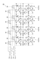
- a binary signal SE0 is input to one end of the above cascaded circuit corresponding to circuit element E0.
- the binary signal SE0 is a signal that takes an ON value or an OFF value in synchronization with the clock CLK supplied to the cascade connection circuit.
- the clock CLK has four cycles.
- the output value of the flip-flop 88 in the circuit region 81D located at the rearmost end of the cascaded circuit is controlled, and the circuit element E0 in the circuit region 81D is controlled.
- the output value of flip-flop 88 in circuit region 81C is controlled according to the value of binary signal SE0 in the second period, and circuit element E0 in circuit region 81C is controlled.
- the output value of flip-flop 88 in circuit region 81B is controlled according to the value of binary signal S E0 in the third period, and circuit element E0 in circuit region 81B is controlled. Then, according to the value of the binary signal SE0 in the fourth period, the output value of the flip-flop 88 in the circuit region 81A is controlled, and the circuit element E0 in the circuit region 81A is controlled.
- the circuit elements E0 of the plurality of circuit regions 81 can be individually controlled.
- the circuit elements E1 of the plurality of circuit regions 81 can also be individually controlled by setting the value of the binary signal SE1 to an arbitrary value for each period of the clock CLK. The same applies to other circuit elements E2 to E8.
- FIG. 10 is a diagram showing another control example of the clock transmission circuit 80.
- the control states of circuit elements E0 and E1 of clock supply portion 82 are similar to the example shown in FIG.
- the circuit regions 81A, 81C, and 81D all the circuit elements E2 to E8 included in the first-stage circuit portion 83, the second-stage circuit portion 84, and the third-stage circuit portion 85 are high impedance. state. Only in the circuit region 81B, the circuit elements E2 to E8 are controlled in the same control state as shown in FIG. In this manner, the clock tree may be configured by only a part of the circuit regions 81 among the plurality of circuit regions 81 .
- the circuit region 81 is limited to the partial circuit region 81 in this manner. clock tree. Thereby, power consumption can be saved.
- FIG. 11 is a flow chart showing a method of manufacturing the clock transmission circuit 80 according to this embodiment.
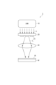
- a common exposure pattern for the circuit region 81 is formed in the first portion 211 of the reticle pattern 21 shown in FIG. ) is subjected to a patch exposure using this exposure pattern (step S1).
- the resist R is developed and cured to form a mask (step S2).
- ion implantation, semiconductor etching, or metal lift-off is performed through a mask to fabricate components of circuit elements E0 to E8 or wirings W1 to W6 (step S3).
- the steps S1 to S3 described above are repeated the number of times required to fabricate the clock transmission circuit 80 (step S4).
- the wafer is cut into individual pieces (step S5).
- the clock transmission circuit 80 having a plurality of circuit regions 81 having circuit patterns common to each other and arranged along the direction D1 can be fabricated on a single substrate.
- FIG. 12 is a diagram schematically showing a clock transmission circuit 100 as a reference example.
- each of a plurality of circuit regions 110 arranged along direction D1 has repeater buffers 101-104.
- Repeater buffers 101 and 102 are alternately connected in series across a plurality of circuit regions 110 .
- the input ends of repeater buffers 103 and 104 are connected to the node between repeater buffer 101 and repeater buffer 102 .
- a clock signal is input from one end of a series circuit composed of repeater buffers 101 and 102 and branched to repeater buffers 103 and 104 in each circuit region 110 while propagating through this series circuit.
- FIG. 13 is a diagram for explaining the effect of clock signal delay. Part (a) of FIG. 13 shows the clock signal input to one end of the series circuit. Part (b) of FIG. 13 shows an example of a serial signal output from a circuit driven by a clock signal output from a circuit region 110 near one end of the series circuit. Part (c) of FIG.
- FIG. 13 shows an example of a serial signal output from a circuit driven by a clock signal output from a circuit region 110 far from one end of the series circuit.
- a delay in some circuit area 110 causes a delay T between serial signals. Therefore, there is a possibility that the accuracy of signal recognition in the circuit that reads the serial signal is lowered.
- a clock tree is used to input clock signals to many circuits at the same timing.
- a plurality of circuit regions having the same circuit pattern are arranged.
- it is easy to form a clock tree within each circuit region it is difficult to form a clock tree across multiple circuit regions.
- it is necessary to prepare many types of exposure patterns which increases the manufacturing cost and complicates the manufacturing process.
- the circuit patterns in each of the plurality of circuit regions 81 are connected to the circuit elements E0 to E6 that can be switched between the high impedance state and the passing state, and the circuit patterns in the circuit regions 81 adjacent to the circuit patterns. and wirings W1 to W6 that are connected to each other.
- the states of the circuit elements E0 to E6 of the plurality of circuit regions 81 are controlled to a predetermined state determined for each circuit region 81, for example, as shown in FIG. clock tree is constructed. Thereby, it is possible to form a clock tree that traverses a plurality of circuit regions 81 having the same circuit pattern. Therefore, clock signal delay between the plurality of circuit regions 81 can be reduced.
- the manufacturing cost can be reduced and the manufacturing process can be simplified.
- the circuit pattern of each circuit region 81 may include multiple stages of circuit portions 83 and 84 configured to bear multiple stages of branching of the clock tree, respectively.
- the circuit portions 83 and 84 of each stage can suitably implement branching of each stage of the clock tree.
- the circuit portion 83 may include circuit elements E2, E3, and E4.
- the output end of circuit element E2, the input end of circuit element E3, and the input end of circuit element E4 are connected to node N2, and the input end of circuit element E2 and the output end of circuit element E3 are connected to node N3.
- the wirings W1 to W6 are the wiring W3 for connecting the node N2 to the node N3 of the circuit region 81 adjacent to one side of the circuit region 81, and the wiring W3 connecting the node N3 to the other side of the circuit region 81. and a wiring W4 for connecting to the node N2 of the circuit region 81 to be connected.
- a circuit portion 83 through which the clock signal propagates receives the clock signal at node N3 (or may be node N2) and can output the clock signal from the output of circuit element E4 as required.
- the propagation direction of the clock signal can be controlled by controlling the states of circuit elements E2 and E3. Therefore, it is possible to easily realize the circuit portion 83 that is particularly responsible for the first stage or middle stage branch.
- the circuit elements E0 to E6 may be of tri-state type.
- each of the circuit elements E0 to E6 can be simply configured with a single functional portion. Since the output resistance value of the circuit elements E0 to E6 in the passing state can be kept low, it is possible to reduce the delay of the clock signal caused by the resistance values of the circuit elements E0 to E6.
- At least one of the A/D converter array 47, the horizontal scanning circuit group 49, and the output circuit group 50 is connected through a clock transmission circuit having the same configuration as the clock transmission circuit 80. receives the clock signal. According to this imaging device 40, it is possible to reduce clock signal delay between a plurality of digital signals. Therefore, it is possible to reduce the frequency of errors when reading the serial signal.
- each circuit region 81 has nine circuit elements E0 to E8. It is possible to implement a clock tree that In other words, each circuit region 81 should have at least two circuit elements E5 and E6.
- circuit elements E0 to E6 are of tristate type, but the circuit elements E0 to E6 are not limited to tristate type as long as they can be switched between the high impedance state and the pass state.
- circuit elements E0-E6 may comprise repeater buffers and switches connected in series with each other. Even in that case, by controlling the switches, the circuit elements E0 to E6 can be switched between the high impedance state and the passing state.
- the circuit elements E7 and E8 forming the circuit portion 85 at the final stage preferably have a configuration for avoiding the potential of the clock signal supplied to the circuit 77 from becoming unstable.
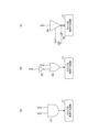
- Parts (a), (b) and (c) of FIG. 14 are circuit diagrams showing configuration examples of such circuit elements.
- the circuit elements shown in parts (a) and (b) of FIG. 14 are configured to include logic circuits.
- the circuit element shown in part (a) of FIG. 14 includes a logical product (AND) element 91 .
- the circuit element consists of AND element 91 only.
- One of the two input terminals of the AND element 91 receives the clock signal Sclk from the preceding circuit portion 84 .
- the control signal Sctrl from the cascaded flip-flops 88 (see FIG. 9) is input to the other input terminal of the two input terminals of the AND element 91 .
- AND element 91 outputs the logical product of clock signal Sclk and control signal Sctrl to circuit 77 .
- the circuit elements consist only of OR elements 92 and NOT elements 93 .
- the clock signal Sclk from the preceding circuit portion 84 is input to one of the two input terminals of the OR element 92 .
- the other input terminal of the two input terminals of the OR element 92 is connected to the output terminal of the NOT element 93 .
- a control signal Sctrl from a cascaded flip-flop 88 (see FIG. 9) is input to the other input terminal via a NOT element 93 .
- OR element 92 outputs to circuit 77 the logical sum of clock signal Sclk and a signal obtained by inverting the logic of control signal Sctrl.
- the circuit element shown in part (c) of FIG. 14 includes a tri-state circuit element 94 and a pull-up resistor 95 .
- the circuit elements consist only of tri-state circuit elements 94 and pull-up resistors 95 .
- a pull-up resistor 95 is connected between the output of the circuit element 94 and the power supply voltage Vdd.
- This circuit element may have a pull-down resistor connected between the output terminal of the circuit element 94 and a reference potential (ground potential) instead of or in addition to the pull-up resistor 95 . Any one of the configurations shown in parts (a), (b) and (c) of FIG. can be prevented.
- the clock transmission circuit 80 can be applied not only to imaging devices but also to various semiconductor devices.
- a clock tree is completed by a plurality of circuit regions 81 having a common circuit pattern.
- a clock tree does not necessarily have to be completed only by a plurality of circuit regions 81 having a common circuit pattern.
- another circuit region that is aligned with the plurality of circuit regions 81 and has a different circuit pattern from the plurality of circuit regions 81 may constitute part of the clock tree.
- REFERENCE SIGNS LIST 1 exposure device 10 light source 20 photomask 21 reticle pattern 30 lens 40 imaging element 41 to 43 circuit area 44 circuit area group 45 pixel array 46 amplifier array , 47... A/D converter array, 48... Memory array, 49... Horizontal scanning circuit group, 50... Output circuit group, 62... Substrate, 70... Clock tree, 76... Wiring, 77... Circuit using clock, 78 ... Repeater buffer 80, 80A, 80B ... Clock transmission circuit 81, 81A to 81D ... Circuit area 82 ... Clock supply part 83 to 85 ... Circuit part 87 ... Wiring 88 ... Flip-flop 91 ...
Landscapes
- Engineering & Computer Science (AREA)
- Multimedia (AREA)
- Signal Processing (AREA)
- Physics & Mathematics (AREA)
- Nonlinear Science (AREA)
- Theoretical Computer Science (AREA)
- General Physics & Mathematics (AREA)
- General Engineering & Computer Science (AREA)
- Electromagnetism (AREA)
- Semiconductor Integrated Circuits (AREA)
- Design And Manufacture Of Integrated Circuits (AREA)
- Transforming Light Signals Into Electric Signals (AREA)
- Manipulation Of Pulses (AREA)
- Exposure And Positioning Against Photoresist Photosensitive Materials (AREA)
Priority Applications (5)
| Application Number | Priority Date | Filing Date | Title |
|---|---|---|---|
| KR1020247019902A KR20240108480A (ko) | 2021-11-22 | 2022-09-29 | 클록 전달 회로, 촬상 소자, 및 클록 전달 회로의 제조 방법 |
| DE112022005614.2T DE112022005614T5 (de) | 2021-11-22 | 2022-09-29 | Taktübertragungsschaltung, bildgebendes Element und Verfahren zur Herstellung einer Taktübertragungsschaltung |
| US18/711,253 US12604116B2 (en) | 2021-11-22 | 2022-09-29 | Clock transmission circuit, imaging element, and method for manufacturing clock transmission circuit |
| GB2408578.9A GB2628256A (en) | 2021-11-22 | 2022-09-29 | Clock transmission circuit, imaging element, and method for manufacturing clock transmission circuit |
| CN202280076757.1A CN118266171A (zh) | 2021-11-22 | 2022-09-29 | 时钟传递电路、摄像元件及时钟传递电路的制造方法 |
Applications Claiming Priority (2)
| Application Number | Priority Date | Filing Date | Title |
|---|---|---|---|
| JP2021-189281 | 2021-11-22 | ||
| JP2021189281A JP7724693B2 (ja) | 2021-11-22 | 2021-11-22 | クロック伝達回路、撮像素子、及びクロック伝達回路の製造方法 |
Publications (1)
| Publication Number | Publication Date |
|---|---|
| WO2023089964A1 true WO2023089964A1 (ja) | 2023-05-25 |
Family
ID=86396770
Family Applications (1)
| Application Number | Title | Priority Date | Filing Date |
|---|---|---|---|
| PCT/JP2022/036575 Ceased WO2023089964A1 (ja) | 2021-11-22 | 2022-09-29 | クロック伝達回路、撮像素子、及びクロック伝達回路の製造方法 |
Country Status (8)
| Country | Link |
|---|---|
| US (1) | US12604116B2 (https=) |
| JP (2) | JP7724693B2 (https=) |
| KR (1) | KR20240108480A (https=) |
| CN (1) | CN118266171A (https=) |
| DE (1) | DE112022005614T5 (https=) |
| GB (1) | GB2628256A (https=) |
| TW (1) | TW202331808A (https=) |
| WO (1) | WO2023089964A1 (https=) |
Citations (2)
| Publication number | Priority date | Publication date | Assignee | Title |
|---|---|---|---|---|
| JP2000243939A (ja) * | 1999-02-17 | 2000-09-08 | Nec Corp | 半導体集積回路装置およびその設計方法 |
| JP2007060036A (ja) * | 2005-08-22 | 2007-03-08 | Micron Technology Inc | 構造化遅延スキューを用いたバッファリング技術 |
Family Cites Families (11)
| Publication number | Priority date | Publication date | Assignee | Title |
|---|---|---|---|---|
| JP2001110708A (ja) | 1999-10-08 | 2001-04-20 | Nikon Corp | 露光装置 |
| JP2001154371A (ja) | 1999-11-30 | 2001-06-08 | Nikon Corp | 回路デバイスや表示デバイスの製造方法、及び大型ディスプレー装置 |
| US6255884B1 (en) * | 2000-02-16 | 2001-07-03 | Pairgain Technologies, Inc. | Uniform clock timing circuit |
| US6879185B2 (en) | 2002-04-05 | 2005-04-12 | Stmicroelectronics Pvt. Ltd. | Low power clock distribution scheme |
| US7382170B2 (en) | 2006-04-18 | 2008-06-03 | Agere Systems Inc. | Programmable delay circuit having reduced insertion delay |
| JP5619434B2 (ja) * | 2010-02-26 | 2014-11-05 | パナソニック株式会社 | 固体撮像装置および撮像装置 |
| US8937491B2 (en) | 2012-11-15 | 2015-01-20 | Xilinx, Inc. | Clock network architecture |
| US9698766B2 (en) | 2014-12-03 | 2017-07-04 | Micron Technology, Inc. | Apparatuses and methods for adjusting timing of signals |
| KR102327498B1 (ko) | 2017-09-12 | 2021-11-17 | 에스케이하이닉스 주식회사 | 듀티 싸이클 보정 회로 및 이를 포함하는 클럭 보정 회로 |
| CN113841103A (zh) | 2019-05-24 | 2021-12-24 | 索尼半导体解决方案公司 | 电路系统 |
| KR102827206B1 (ko) * | 2019-09-02 | 2025-07-01 | 삼성전자주식회사 | 클럭 트리를 포함하는 이미지 센서 및 어드레스 디코더, 이미지 센서를 포함하는 이미지 처리 시스템 |
-
2021
- 2021-11-22 JP JP2021189281A patent/JP7724693B2/ja active Active
-
2022
- 2022-09-29 CN CN202280076757.1A patent/CN118266171A/zh active Pending
- 2022-09-29 US US18/711,253 patent/US12604116B2/en active Active
- 2022-09-29 WO PCT/JP2022/036575 patent/WO2023089964A1/ja not_active Ceased
- 2022-09-29 DE DE112022005614.2T patent/DE112022005614T5/de active Pending
- 2022-09-29 GB GB2408578.9A patent/GB2628256A/en active Pending
- 2022-09-29 KR KR1020247019902A patent/KR20240108480A/ko not_active Withdrawn
- 2022-10-28 TW TW111141076A patent/TW202331808A/zh unknown
-
2025
- 2025-08-05 JP JP2025130622A patent/JP2025168357A/ja active Pending
Patent Citations (2)
| Publication number | Priority date | Publication date | Assignee | Title |
|---|---|---|---|---|
| JP2000243939A (ja) * | 1999-02-17 | 2000-09-08 | Nec Corp | 半導体集積回路装置およびその設計方法 |
| JP2007060036A (ja) * | 2005-08-22 | 2007-03-08 | Micron Technology Inc | 構造化遅延スキューを用いたバッファリング技術 |
Also Published As
| Publication number | Publication date |
|---|---|
| US20250008241A1 (en) | 2025-01-02 |
| DE112022005614T5 (de) | 2024-09-19 |
| US12604116B2 (en) | 2026-04-14 |
| CN118266171A (zh) | 2024-06-28 |
| TW202331808A (zh) | 2023-08-01 |
| KR20240108480A (ko) | 2024-07-09 |
| GB202408578D0 (en) | 2024-07-31 |
| JP7724693B2 (ja) | 2025-08-18 |
| JP2023076093A (ja) | 2023-06-01 |
| GB2628256A (en) | 2024-09-18 |
| JP2025168357A (ja) | 2025-11-07 |
Similar Documents
| Publication | Publication Date | Title |
|---|---|---|
| CN101753864B (zh) | 固态成像装置和使用该固态成像装置的成像系统 | |
| JP5127862B2 (ja) | 固体撮像装置 | |
| JP3481193B2 (ja) | 改良式デジタル画像化回路及びその方法 | |
| WO2023089964A1 (ja) | クロック伝達回路、撮像素子、及びクロック伝達回路の製造方法 | |
| US20170104948A1 (en) | Latch based parallel-to-serial readout circuitry and image sensor utilizing the circuitry | |
| CN101107843A (zh) | 固态摄像装置及其驱动方法 | |
| US6944352B1 (en) | Circuitry for determining median of image portions | |
| US10042000B2 (en) | Method and apparatus for high frequency analog-to-digital conversion | |
| JP6555239B2 (ja) | 半導体集積回路及び半導体集積回路のクロック供給方法 | |
| US7199915B2 (en) | Buffers for light modulation elements in spatial light modulators | |
| EP4180839A1 (en) | Tof sensor | |
| CN100546346C (zh) | 固体摄像装置 | |
| US5943491A (en) | Control circuit of mutual exclusion elements | |
| KR100264641B1 (ko) | 지연회로 | |
| CN112995547B (zh) | 图像感测装置 | |
| JP7004555B2 (ja) | イメージセンサ | |
| JP2020043541A (ja) | 固体撮像素子 | |
| JP2814032B2 (ja) | スキャンパス装置およびそれを含む半導体集積回路装置 | |
| US6292043B1 (en) | Semiconductor integrated circuit device | |
| JP4388871B2 (ja) | 半導体撮像装置 | |
| CN117294967A (zh) | 线性图像传感器及其控制方法 | |
| US20050213179A1 (en) | Angled strobe lines for high aspect ratio spatial light modulator | |
| JPH1010194A (ja) | 半導体集積回路 | |
| JPS58124364A (ja) | 画像読取り装置 |
Legal Events
| Date | Code | Title | Description |
|---|---|---|---|
| 121 | Ep: the epo has been informed by wipo that ep was designated in this application |
Ref document number: 22895250 Country of ref document: EP Kind code of ref document: A1 |
|
| WWE | Wipo information: entry into national phase |
Ref document number: 18711253 Country of ref document: US Ref document number: 202280076757.1 Country of ref document: CN |
|
| ENP | Entry into the national phase |
Ref document number: 202408578 Country of ref document: GB Kind code of ref document: A Free format text: PCT FILING DATE = 20220929 Ref document number: 20247019902 Country of ref document: KR Kind code of ref document: A |
|
| WWE | Wipo information: entry into national phase |
Ref document number: 1020247019902 Country of ref document: KR Ref document number: 2408578.9 Country of ref document: GB |
|
| WWP | Wipo information: published in national office |
Ref document number: 2408578.9 Country of ref document: GB |
|
| 122 | Ep: pct application non-entry in european phase |
Ref document number: 22895250 Country of ref document: EP Kind code of ref document: A1 |
|
| WWW | Wipo information: withdrawn in national office |
Ref document number: 1020247019902 Country of ref document: KR |
|
| WWG | Wipo information: grant in national office |
Ref document number: 18711253 Country of ref document: US |