WO2023089959A1 - 半導体回路 - Google Patents
半導体回路 Download PDFInfo
- Publication number
- WO2023089959A1 WO2023089959A1 PCT/JP2022/035906 JP2022035906W WO2023089959A1 WO 2023089959 A1 WO2023089959 A1 WO 2023089959A1 JP 2022035906 W JP2022035906 W JP 2022035906W WO 2023089959 A1 WO2023089959 A1 WO 2023089959A1
- Authority
- WO
- WIPO (PCT)
- Prior art keywords
- transistor
- node
- voltage
- source
- memory cell
- Prior art date
- Legal status (The legal status is an assumption and is not a legal conclusion. Google has not performed a legal analysis and makes no representation as to the accuracy of the status listed.)
- Ceased
Links
Images







Classifications
-
- G—PHYSICS
- G11—INFORMATION STORAGE
- G11C—STATIC STORES
- G11C11/00—Digital stores characterised by the use of particular electric or magnetic storage elements; Storage elements therefor
- G11C11/02—Digital stores characterised by the use of particular electric or magnetic storage elements; Storage elements therefor using magnetic elements
- G11C11/16—Digital stores characterised by the use of particular electric or magnetic storage elements; Storage elements therefor using magnetic elements using elements in which the storage effect is based on magnetic spin effect
- G11C11/165—Auxiliary circuits
- G11C11/1673—Reading or sensing circuits or methods
-
- G—PHYSICS
- G11—INFORMATION STORAGE
- G11C—STATIC STORES
- G11C11/00—Digital stores characterised by the use of particular electric or magnetic storage elements; Storage elements therefor
- G11C11/02—Digital stores characterised by the use of particular electric or magnetic storage elements; Storage elements therefor using magnetic elements
- G11C11/16—Digital stores characterised by the use of particular electric or magnetic storage elements; Storage elements therefor using magnetic elements using elements in which the storage effect is based on magnetic spin effect
-
- G—PHYSICS
- G11—INFORMATION STORAGE
- G11C—STATIC STORES
- G11C11/00—Digital stores characterised by the use of particular electric or magnetic storage elements; Storage elements therefor
- G11C11/02—Digital stores characterised by the use of particular electric or magnetic storage elements; Storage elements therefor using magnetic elements
- G11C11/16—Digital stores characterised by the use of particular electric or magnetic storage elements; Storage elements therefor using magnetic elements using elements in which the storage effect is based on magnetic spin effect
- G11C11/165—Auxiliary circuits
- G11C11/1659—Cell access
-
- G—PHYSICS
- G11—INFORMATION STORAGE
- G11C—STATIC STORES
- G11C11/00—Digital stores characterised by the use of particular electric or magnetic storage elements; Storage elements therefor
- G11C11/02—Digital stores characterised by the use of particular electric or magnetic storage elements; Storage elements therefor using magnetic elements
- G11C11/16—Digital stores characterised by the use of particular electric or magnetic storage elements; Storage elements therefor using magnetic elements using elements in which the storage effect is based on magnetic spin effect
- G11C11/165—Auxiliary circuits
- G11C11/1675—Writing or programming circuits or methods
-
- G—PHYSICS
- G11—INFORMATION STORAGE
- G11C—STATIC STORES
- G11C11/00—Digital stores characterised by the use of particular electric or magnetic storage elements; Storage elements therefor
- G11C11/02—Digital stores characterised by the use of particular electric or magnetic storage elements; Storage elements therefor using magnetic elements
- G11C11/16—Digital stores characterised by the use of particular electric or magnetic storage elements; Storage elements therefor using magnetic elements using elements in which the storage effect is based on magnetic spin effect
- G11C11/165—Auxiliary circuits
- G11C11/1693—Timing circuits or methods
-
- G—PHYSICS
- G11—INFORMATION STORAGE
- G11C—STATIC STORES
- G11C11/00—Digital stores characterised by the use of particular electric or magnetic storage elements; Storage elements therefor
- G11C11/02—Digital stores characterised by the use of particular electric or magnetic storage elements; Storage elements therefor using magnetic elements
- G11C11/16—Digital stores characterised by the use of particular electric or magnetic storage elements; Storage elements therefor using magnetic elements using elements in which the storage effect is based on magnetic spin effect
- G11C11/165—Auxiliary circuits
- G11C11/1697—Power supply circuits
-
- G—PHYSICS
- G11—INFORMATION STORAGE
- G11C—STATIC STORES
- G11C13/00—Digital stores characterised by the use of storage elements not covered by groups G11C11/00, G11C23/00, or G11C25/00
- G11C13/0002—Digital stores characterised by the use of storage elements not covered by groups G11C11/00, G11C23/00, or G11C25/00 using resistive RAM [RRAM] elements
- G11C13/0004—Digital stores characterised by the use of storage elements not covered by groups G11C11/00, G11C23/00, or G11C25/00 using resistive RAM [RRAM] elements comprising amorphous/crystalline phase transition cells
-
- G—PHYSICS
- G11—INFORMATION STORAGE
- G11C—STATIC STORES
- G11C13/00—Digital stores characterised by the use of storage elements not covered by groups G11C11/00, G11C23/00, or G11C25/00
- G11C13/0002—Digital stores characterised by the use of storage elements not covered by groups G11C11/00, G11C23/00, or G11C25/00 using resistive RAM [RRAM] elements
- G11C13/0021—Auxiliary circuits
- G11C13/0038—Power supply circuits
-
- G—PHYSICS
- G11—INFORMATION STORAGE
- G11C—STATIC STORES
- G11C13/00—Digital stores characterised by the use of storage elements not covered by groups G11C11/00, G11C23/00, or G11C25/00
- G11C13/0002—Digital stores characterised by the use of storage elements not covered by groups G11C11/00, G11C23/00, or G11C25/00 using resistive RAM [RRAM] elements
- G11C13/0021—Auxiliary circuits
- G11C13/004—Reading or sensing circuits or methods
-
- G—PHYSICS
- G11—INFORMATION STORAGE
- G11C—STATIC STORES
- G11C13/00—Digital stores characterised by the use of storage elements not covered by groups G11C11/00, G11C23/00, or G11C25/00
- G11C13/0002—Digital stores characterised by the use of storage elements not covered by groups G11C11/00, G11C23/00, or G11C25/00 using resistive RAM [RRAM] elements
- G11C13/0021—Auxiliary circuits
- G11C13/0069—Writing or programming circuits or methods
-
- G—PHYSICS
- G11—INFORMATION STORAGE
- G11C—STATIC STORES
- G11C5/00—Details of stores covered by group G11C11/00
- G11C5/06—Arrangements for interconnecting storage elements electrically, e.g. by wiring
- G11C5/063—Voltage and signal distribution in integrated semi-conductor memory access lines, e.g. word-line, bit-line, cross-over resistance, propagation delay
-
- G—PHYSICS
- G11—INFORMATION STORAGE
- G11C—STATIC STORES
- G11C7/00—Arrangements for writing information into, or reading information out from, a digital store
- G11C7/06—Sense amplifiers; Associated circuits, e.g. timing or triggering circuits
-
- G—PHYSICS
- G11—INFORMATION STORAGE
- G11C—STATIC STORES
- G11C7/00—Arrangements for writing information into, or reading information out from, a digital store
- G11C7/06—Sense amplifiers; Associated circuits, e.g. timing or triggering circuits
- G11C7/065—Differential amplifiers of latching type
-
- G—PHYSICS
- G11—INFORMATION STORAGE
- G11C—STATIC STORES
- G11C7/00—Arrangements for writing information into, or reading information out from, a digital store
- G11C7/14—Dummy cell management; Sense reference voltage generators
Definitions
- the present disclosure relates to a semiconductor circuit capable of storing data.
- a semiconductor circuit often includes a non-volatile memory circuit using, for example, a resistance change memory element.
- a resistance change memory element for example, Japanese Unexamined Patent Application Publication No. 2002-200003 discloses a memory circuit that causes a current to flow through a memory element using a clamp transistor and reads out data based on a voltage corresponding to the resistance value of the memory element.
- a semiconductor circuit includes a first memory cell, a first signal line, a second memory cell, a second signal line, a sense amplifier, a first switch, and a second switch.
- a first memory cell has a first storage element. The first signal line is connected to the first memory cell.
- a second memory cell has a second storage element. A second signal line is connected to the second memory cell.
- the sense amplifier has a latch circuit, a first transistor, a second transistor and a third transistor.
- the latch circuit can apply an inverted voltage of the voltage of the first node to the second node, and can apply an inverted voltage of the voltage of the second node to the first node.
- a first transistor has a source, a gate and a drain connected to the first node.
- a second transistor has a source, a gate and a drain connected to the second node.
- a third transistor has a source, a gate to which a control voltage can be applied, and a drain connected to one or both of the source of the first transistor and the source of the second transistor. is.
- the first switch can connect the first signal line and the first node when turned on.
- the second switch can connect the second signal line and the second node when turned on.
- the latch circuit applies an inverted voltage of the voltage of the first node to the second node, and applies an inverted voltage of the voltage of the second node to the first node. be done.
- the gate and drain of the first transistor are connected to the first node and the gate and drain of the second transistor are connected to the second node.
- a drain of the third transistor is connected to one or both of the source of the first transistor and the source of the second transistor, and a control voltage is applied to the gate.
- the first node is connected to the first signal line connected to the first memory cell by turning on the first switch.
- the second node is connected to the second signal line connected to the second memory cell by turning on the second switch.
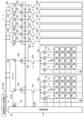
- FIG. 1 is a circuit diagram showing a configuration example of a semiconductor circuit according to an embodiment of the present disclosure
- FIG. 2 is a circuit diagram showing a configuration example of a memory cell array shown in FIG. 1
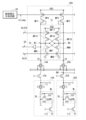
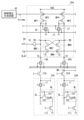
- FIG. 2 is a circuit diagram showing one configuration example of a sense amplifier and a control voltage generation circuit shown in FIG. 1
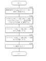
- FIG. 2 is a flowchart showing an operation example of the semiconductor circuit shown in FIG. 1
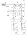
- FIG. 4 is a circuit diagram showing a configuration example of a sense amplifier according to a comparative example
- FIG. 11 is a circuit diagram showing a configuration example of a sense amplifier according to a modification
- 7 is a flow chart showing an operation example of the semiconductor circuit including the sense amplifier shown in FIG. 6;
- FIG. 1 is a circuit diagram showing a configuration example of a semiconductor circuit according to an embodiment of the present disclosure
- FIG. 2 is a circuit diagram showing a configuration example of a memory cell array shown in FIG. 1
- FIG. 2 is a circuit diagram showing one configuration example of
- FIG. 11 is a circuit diagram showing a configuration example of a sense amplifier according to another modification;
- FIG. 11 is a circuit diagram showing a configuration example of a sense amplifier according to another modification;
- FIG. 11 is a circuit diagram showing a configuration example of a sense amplifier according to another modification;
- FIG. 11 is a circuit diagram showing a configuration example of a sense amplifier according to another modification;
- FIG. 11 is a circuit diagram showing a configuration example of a sense amplifier according to another modification;
- FIG. 11 is a circuit diagram showing a configuration example of a sense amplifier according to another modification;
- FIG. 11 is a circuit diagram showing a configuration example of a sense amplifier according to another modification;
- 15 is a flow chart showing an operation example of the semiconductor circuit including the sense amplifier shown in FIG. 14;
- FIG. 14 is a flow chart showing an operation example of the semiconductor circuit including the sense amplifier shown in FIG. 14;
- FIG. 14 is a flow chart showing an operation example of the semiconductor circuit including the sense amplifier shown in FIG. 14
- FIG. 11 is a circuit diagram showing a configuration example of a sense amplifier according to another modification
- 17 is a flow chart showing an operation example of the semiconductor circuit including the sense amplifier shown in FIG. 16
- FIG. 11 is a circuit diagram showing a configuration example of a sense amplifier according to another modification
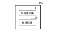
- FIG. 11 is a block diagram showing a configuration example of a semiconductor circuit according to another modified example
- FIG. 1 shows a configuration example of a semiconductor circuit (semiconductor circuit 1) according to an embodiment.
- the semiconductor circuit 1 is a nonvolatile memory circuit that stores data.
- the semiconductor circuit 1 includes a control circuit 9, four memory cell arrays 10 (memory cell arrays 10A, 10B, 10C and 10D), four transistors 15 (transistors 15A, 15B, 15C and 15D), and four transfer gates 16 ( transfer gates 16A, 16B, 16C, 16D), four memory cell arrays 20 (memory cell arrays 20A, 20B, 20C, 20D), four transistors 25 (transistors 25A, 25B, 25C, 25D), and four transfer gates 26 (transfer gates 26A, 26B, 26C, 26D), four sense amplifiers 30 (sense amplifiers 30A, 30B, 30C, 30D), and a control voltage generation circuit 40.
- four circuit groups each including memory cell arrays 10 and 20, transistors 15 and 25, transfer gates 16
- the control circuit 9 is configured to control the operation of the semiconductor circuit 1 . Specifically, the control circuit 9 controls the operation of the semiconductor circuit 1 to write data into the four memory cell arrays 10 based on the externally supplied write command and write data. The operation of the semiconductor circuit 1 is controlled to read data from the four memory cell arrays 10 based on the read command.
- the memory cell arrays 10A, 10B, 10C, and 10D are configured to store data.
- FIG. 2 shows a configuration example of the memory cell array 10A.
- the configuration of memory cell arrays 10B, 10C and 10D is similar to that of memory cell array 10A.
- the memory cell array 10A has multiple word lines WL, four bit lines BL, multiple memory cells MC, four transistors 111-114, and four transfer gates 11-14.
- a plurality of word lines WL extend in the horizontal direction in FIGS. 1 and 2 and are arranged in parallel in the vertical direction.
- a plurality of word lines WL in each of the four memory cell arrays 10A, 10B, 10C and 10D are connected to each other between the memory cell arrays.
- a plurality of word lines WL are connected to a control circuit 9 from which control signals for selecting memory cells MC are supplied.
- the four bit lines BL extend vertically in FIGS. 1 and 2 and are arranged side by side in the horizontal direction.
- a plurality of bit lines BL are connected to four transfer gates 11-14, respectively.
- Each of the plurality of memory cells MC is configured to store data.
- the plurality of memory cells MC includes four columns of memory cells MC corresponding to four bit lines BL in this example.
- a memory cell MC has a transistor 101 and a memory element 102 .
- the transistor 101 is an N-type MOS (Metal Oxide Semiconductor) transistor having a source connected to the bit line BL, a gate connected to the word line WL, and a drain connected to the storage element 102 .
- N-type MOS Metal Oxide Semiconductor
- the memory element 102 is a non-volatile memory element, and is configured to be able to store information by utilizing the fact that the resistance state reversibly changes according to the direction of current flow.
- the storage element 102 is a magnetic tunnel junction (MTJ) element in this example.
- One end of the memory element 102 is connected to the drain of the transistor 101 and the other end is connected to one of the transistors 111-114.
- the other end of the memory element 102 in the memory cell MC in the first column from the left is connected to the drain of the transistor 111, and the other end of the memory cell MC in the second column from the left is connected to the drain of the transistor 112.
- the other end of the memory element 102 in the memory cell MC on the third column from the left is connected to the drain of the transistor 113, and the other end of the memory element 102 in the memory cell MC on the fourth column from the left is connected to the drain of the transistor 114. Connected to drain.
- the resistance state of the memory element 102 is set according to the direction of the current when the current value of the current flowing between both ends is greater than the current threshold TH.
- the resistance state can be a low resistance state RL or a high resistance state RH.
- the low resistance state RL is a state in which the resistance value between both ends is low
- the high resistance state RH is a state in which the resistance value between the ends is high.
- the resistance state of the memory element 102 is set to the high resistance state.
- the resistance state of the memory element 102 is set to the low resistance state RL.
- FIG. 2 omits illustration of a configuration for performing a write operation for setting the resistance state of the memory element 102, for example, in FIG. Circuitry is added that allows current to flow from one end of 102 to the other or from the other end of storage element 102 to one end.
- control circuit 9 selects one of the plurality of memory cells MC based on the address signal included in the write command, and changes the resistance state of storage element 102 of the selected memory cell MC. , the low resistance state RL or the high resistance state RH.
- Each of the four transistors 111 to 114 is an N-type MOS transistor and provided corresponding to each of the four columns of memory cells MC.
- the drain of the transistor 111 is connected to the other end of the storage element 102 in the plurality of memory cells MC in the first column from the left, the gate is supplied with a control signal from the control circuit 9, and the source is grounded.
- the transistor 112 has a drain connected to the other end of the memory element 102 in the plurality of memory cells MC on the second column from the left, a gate supplied with a control signal from the control circuit 9, and a source grounded.
- the drain of the transistor 113 is connected to the other end of the memory element 102 in the plurality of memory cells MC in the third column from the left, the gate is supplied with a control signal from the control circuit 9, and the source is grounded.
- the drain of the transistor 114 is connected to the other end of the memory element 102 in the plurality of memory cells MC on the fourth column from the left, the gate is supplied with a control signal from the control circuit 9, and the source is grounded.
- Each of the four transfer gates 11 to 14 is provided corresponding to each of four columns of memory cells MC.
- One end of the transfer gate 11 is connected to the source of the transistor 15A, and the other end is connected to the first bit line BL from the left.
- Transfer gate 11 is configured to be turned on and off based on a control signal from control circuit 9 .
- One end of the transfer gate 12 is connected to the source of the transistor 15A, and the other end is connected to the second bit line BL from the left.
- Transfer gate 12 is configured to be turned on and off based on a control signal from control circuit 9 .
- One end of the transfer gate 13 is connected to the source of the transistor 15A, and the other end is connected to the third bit line BL from the left.
- Transfer gate 13 is configured to be turned on and off based on a control signal from control circuit 9 .
- One end of the transfer gate 14 is connected to the source of the transistor 15A, and the other end is connected to the fourth bit line BL from the left.
- Transfer gate 14 is configured to be turned on and off based on a control signal from control circuit 9 .
- transfer gate 11 When transfer gate 11 is turned on, four transfer gates 11 in memory cell arrays 10A-10D are turned on.
- the transistor 15A (FIG. 1) is an N-type MOS transistor having a drain connected to the transfer gate 16A, a gate supplied with a control signal from the control circuit 9, and a source connected to the four transfer gates 11 to 11 in the memory cell array 10A. 14 is connected to one end.
- the transistor 15B has a drain connected to the transfer gate 16B, a gate supplied with a control signal from the control circuit 9, and a source connected to one end of the four transfer gates 11 to 14 in the memory cell array 10B.
- the transistor 15C has a drain connected to the transfer gate 16C, a gate supplied with a control signal from the control circuit 9, and a source connected to one end of the four transfer gates 11 to 14 in the memory cell array 10C.
- the transistor 15D has a drain connected to the transfer gate 16D, a gate supplied with a control signal from the control circuit 9, and a source connected to one end of the four transfer gates 11 to 14 in the memory cell array 10D.
- the transfer gate 16A has one end connected to the terminal TD of the sense amplifier 30A and the other end connected to the drain of the transistor 15A.
- the transfer gate 16A is configured to be turned on and off based on a control signal from the control circuit 9.
- FIG. Similarly, the transfer gate 16B has one end connected to the terminal TD of the sense amplifier 30B and the other end connected to the drain of the transistor 15B.
- the transfer gate 16B is configured to be turned on and off based on the control signal from the control circuit 9.
- FIG. One end of the transfer gate 16C is connected to the terminal TD of the sense amplifier 30C, and the other end is connected to the drain of the transistor 15C.
- the transfer gate 16C is configured to be turned on and off based on the control signal from the control circuit 9.
- One end of the transfer gate 16D is connected to the terminal TD of the sense amplifier 30D, and the other end is connected to the drain of the transistor 15D.
- the transfer gate 16 ⁇ /b>D is configured to be turned on and off based on the control signal from the control circuit 9 .
- control circuit 9 selects one of the plurality of memory cells MC in each of memory cell arrays 10A, 10B, 10C and 10D based on the address signal included in the read command. . Specifically, control circuit 9 turns on one of transfer gates 11-14 by supplying a control signal to transfer gates 11-14. For example, when turning on the transfer gates 11, the control circuit 9 turns on the four transfer gates 11 in the memory cell arrays 10A to 10D. Further, the control circuit 9 supplies control signals to the transistors 111 to 114 to turn on the transistors corresponding to the transfer gates to be turned on among the transfer gates 11 to 14 .
- control circuit 9 turns on the transistor 111 when turning on the transfer gate 11, turns on the transistor 112 when turning on the transfer gate 12, and turns on the transfer gate 13.
- the transistor 114 is turned on.
- the control circuit 9 turns on the four transistors 111 in the memory cell arrays 10A to 10D.
- the control circuit 9 sets the voltage of one of the word lines WL to a high level. Thereby, control circuit 9 selects one of the plurality of memory cells MC in each of memory cell arrays 10A-10D.
- Control circuit 9 connects selected memory cell MC in memory cell array 10A to terminal TD of sense amplifier 30A via transistor 15A and transfer gate 16A, and connects selected memory cell MC in memory cell array 10B to terminal TD of sense amplifier 30A. connecting to terminal TD of sense amplifier 30B via transistor 15B and transfer gate 16B, connecting selected memory cell MC in memory cell array 10C to terminal TD of sense amplifier 30C via transistor 15C and transfer gate 16C, A memory cell MC selected in the memory cell array 10D is connected to a terminal TD of a sense amplifier 30D via a transistor 15D and a transfer gate 16D.
- the memory cell arrays 20A, 20B, 20C, and 20D are configured to store reference data, which is predetermined data. That is, the memory cell arrays 10A, 10B, 10C and 10D store arbitrary data, and the memory cell arrays 20A, 20B, 20C and 20D store reference data as predetermined data.
- the configuration of memory cell arrays 20A-20D is similar to the configuration of memory cell array 10A (FIG. 2).
- the transistor 25A is an N-type MOS transistor having a drain connected to the node NR, a gate supplied with a control signal from the control circuit 9, and a source connected to one end of the four transfer gates 11 to 14 in the memory cell array 20A. be done.
- transistor 25B has a drain connected to node NR, a gate supplied with a control signal from control circuit 9, and a source connected to one end of four transfer gates 11-14 in memory cell array 20B.
- the transistor 25C has a drain connected to the node NR, a gate supplied with a control signal from the control circuit 9, and a source connected to one end of the four transfer gates 11 to 14 in the memory cell array 20C.
- the transistor 25D has a drain connected to the node NR, a gate supplied with a control signal from the control circuit 9, and a source connected to one end of the four transfer gates 11 to 14 in the memory cell array 20D.
- transfer gate 26A One end of the transfer gate 26A is connected to the terminal TR of the sense amplifier 30A, and the other end is connected to the node NR.
- the transfer gate 26A is configured to be turned on and off based on a control signal from the control circuit 9.
- transfer gate 26B has one end connected to terminal TR of sense amplifier 30B and the other end connected to node NR.
- the transfer gate 26B is configured to be turned on and off based on a control signal from the control circuit 9.
- One end of the transfer gate 26C is connected to the terminal TR of the sense amplifier 30C, and the other end is connected to the node NR.
- Transfer gate 26 ⁇ /b>C is configured to be turned on and off based on a control signal from control circuit 9 .
- One end of the transfer gate 26D is connected to the terminal TR of the sense amplifier 30D, and the other end is connected to the node NR.
- the transfer gate 26D is configured to be turned on and off based on a control signal from the control circuit 9.
- drains of transistors 25A, 25B, 25C and 25D and the other ends of transfer gates 26A, 26B, 26C and 26D are connected to each other at node NR.
- control circuit 9 selects one of the plurality of memory cells MC in each of the memory cell arrays 20A, 20B, 20C and 20D. Specifically, control circuit 9 turns on one of transfer gates 11-14 by supplying a control signal to transfer gates 11-14. For example, when turning on the transfer gates 11, the control circuit 9 turns on the four transfer gates 11 in the memory cell arrays 20A to 20D. Further, the control circuit 9 supplies control signals to the transistors 111 to 114 to turn on the transistors corresponding to the transfer gates to be turned on among the transfer gates 11 to 14 . Specifically, the control circuit 9 turns on the transistor 111 when turning on the transfer gate 11, turns on the transistor 112 when turning on the transfer gate 12, and turns on the transfer gate 13.
- the control circuit 9 turns on the four transistors 111 in the memory cell arrays 20A to 20D. Then, the control circuit 9 sets the voltage of one of the word lines WL to a high level. Thereby, control circuit 9 selects one of the plurality of memory cells MC in each of memory cell arrays 20A-20D.
- the memory cell arrays 20A, 20B, 20C, and 20D store reference data as predetermined data.
- the four memory elements 102 of the four selected memory cells MC are two memory elements 102 whose resistance state is the low resistance state RL and two memory elements 102 whose resistance state is the high resistance state. It contains two storage elements 102 that are in state RH.
- Control circuit 9 connects selected memory cells MC in each of memory cell arrays 20A-20D to terminals TR of sense amplifiers 30A-30D via transistors 25A-25D and transfer gates 26A-26D. As a result, each of the terminals TR of the sense amplifiers 30A to 30D is equivalently connected to a memory element having the same resistance value as the average value of the resistance values of these four memory elements 102.
- sense amplifier 30A compares the voltage at terminal TD and the voltage at terminal TR to read data stored in memory cell array 10A and supplies control circuit 9 with signal SD indicating the read result.
- sense amplifier 30B reads data stored in memory cell array 10B by comparing the voltage at terminal TD and the voltage at terminal TR, and outputs signal SD indicating the read result to control circuit 9.
- the sense amplifier 30C compares the voltage at the terminal TD and the voltage at the terminal TR to read the data stored in the memory cell array 10C and supplies the control circuit 9 with a signal SD indicating the read result.
- the sense amplifier 30D compares the voltage at the terminal TD and the voltage at the terminal TR to read the data stored in the memory cell array 10D and supplies the control circuit 9 with a signal SD indicating the read result.
- FIG. 3 shows a configuration example of the sense amplifier 30A.
- the configurations of sense amplifiers 30B, 30C and 30D are similar to the configuration of sense amplifier 30A.
- FIG. 3 also shows a part of the memory cell arrays 10A and 20A, the transistors 15A and 25A, the transfer gates 16A and 26A, and the control voltage generation circuit 40.
- FIG. The sense amplifier 30A has transistors MP1 to MP4, a latch circuit 31, and a buffer 32.
- the transistors MP1 to MP4 are P-type MOS transistors.
- the gate and drain of transistor MP1 are connected to node N1, and the source is connected to the drain of transistor MP3.
- the gate and drain of transistor MP2 are connected to node N2, and the source is connected to the drain of transistor MP4.
- the control voltage Vclamp is supplied from the control voltage generation circuit 40 to the gate of the transistor MP3, the source is connected to the power supply node of the power supply voltage VDD, and the drain is connected to the source of the transistor MP1.
- the control voltage Vclamp is supplied from the control voltage generation circuit 40 to the gate of the transistor MP4, the source is connected to the power supply node of the power supply voltage VDD, and the drain is connected to the source of the transistor MP2.
- the latch circuit 31 is configured to perform a latch operation based on the voltage of the node N1 connected to the terminal TD and the voltage of the node N2 connected to the terminal TR.
- the latch circuit 31 has transistors MN5 to MN8.
- the transistors MN5 to MN8 are N-type MOS transistors.
- Transistor MN5 has a gate connected to node N2, a drain connected to node N1, and a source connected to the drain of transistor MN7.
- Transistor MN6 has a gate connected to node N1, a drain connected to node N2, and a source connected to the drain of transistor MN8.
- a signal RLAT is supplied from the control circuit 9 to the gate of the transistor MN7, the drain is connected to the source of the transistor MN5, and the source is grounded.
- a signal RLAT is supplied from the control circuit 9 to the gate of the transistor MN8, the drain is connected to the source of the transistor MN6, and the source is grounded.
- the buffer 32 is configured to output the latch result of the latch circuit 31 as the signal SD.
- Buffer 32 has an input terminal connected to node N1 and an output terminal connected to control circuit 9 .
- the transistor MP3 of the sense amplifier 30A causes a current corresponding to the control voltage Vclamp to flow from the power supply node of the power supply voltage VDD to the memory cell array 10A via the transistor MP1, the transfer gate 16A, and the transistor 15A.
- the transistors MP3 of the sense amplifiers 30B-30D transmit a current corresponding to the control voltage Vclamp from the power supply node of the power supply voltage VDD via four transistors MP2, transfer gates 26A to 26D, and transistors 25A to 25D to the memory cell array. Flow towards 20A-20D.
- the latch circuit 31 performs a latch operation based on the voltages of the nodes N1 and N2. Specifically, in the latch circuit 31, when the signal RLAT becomes high level, the transistors MN7 and MN8 are turned on, and the sources of the transistors MN5 and MN6 are grounded. Transistors MN5 and MN6 perform a full feedback operation based on the voltage of node N1 and the voltage of node N2. For example, when the voltage of the node N1 is higher than the voltage of the node N2, the voltage of the node N1 is brought to a high level and the voltage of the node N2 is brought to a low level by performing the full feedback operation.
- the buffer 32 outputs the latch result of the latch circuit 31 as a signal SD.
- the control voltage generation circuit 40 is configured to generate a control voltage Vclamp based on an instruction from the control circuit 9 and supply this control voltage Vclamp to the sense amplifiers 30A to 30D in the read operation.
- the control voltage generation circuit 40 includes a voltage generation circuit 51, an operational amplifier 52, a switch 53, a transistor 41, a memory element 42, a transistor 43, a transfer gate 44, and a transistor 45. , a transfer gate 46 and transistors 47 and 48 .
- Transistor 41, storage element 42, transistor 43, transfer gate 44, transistor 45, transfer gate 46, and transistors 47 and 48 are each in the path from memory cell arrays 10 and 20 to sense amplifier 30, as shown in FIG. configured to be a replica of the element.
- Transistors 41, 43 and 45 are N-type MOS transistors, and transistors 47 and 48 are P-type MOS transistors.
- the voltage generation circuit 51 is configured to generate the voltage VREF.
- the operational amplifier 52 is configured to generate the voltage Vclamp by amplifying the voltage difference between the voltage of the positive input terminal and the voltage of the negative input terminal, and to output this voltage Vclamp from the output terminal.
- the output terminal of operational amplifier 52 is connected to switch 53, the gate of transistor 48, and the gates of transistors MP3 and MP4 in each of sense amplifiers 30A-30D.
- One end of the switch 53 is connected to the power supply node of the power supply voltage VDD, and the other end is connected to the output terminal of the operational amplifier 52 .
- This switch 53 is turned on and off based on a control signal supplied from the control circuit 9 .
- the gate of the transistor 41 is connected to the power supply node of the power supply voltage VDD, the drain is connected to the storage element 42, and the source is grounded. Transistor 41 is set to an ON state. Transistor 41 has the same characteristics as transistors 111 - 114 in memory cell arrays 10 and 20 .
- Memory element 42 One end of the memory element 42 is connected to the source of the transistor 43 and the positive input terminal of the operational amplifier 52 , and the other end is connected to the drain of the transistor 41 .
- Memory element 42 has the same characteristics as memory element 102 in memory cell arrays 10 and 20 .
- the resistance state of the memory element 42 is set to the low resistance state RL.
- the transistor 43 has a gate connected to the power supply node of the power supply voltage VDD, a drain connected to the transfer gate 44 , and a source connected to one end of the storage element 42 and the positive input terminal of the operational amplifier 52 .
- Transistor 43 is set to an ON state.
- Transistor 43 has the same characteristics as transistor 101 in memory cell arrays 10 and 20 .
- the transfer gate 44 has one end connected to the source of the transistor 45 and the other end connected to the drain of the transistor 43 . Transfer gate 44 is set to an ON state. Transfer gate 44 has the same characteristics as transfer gates 11 - 14 in memory cell arrays 10 and 20 .
- the transistor 45 has a gate connected to the power supply node of the power supply voltage VDD, a drain connected to the transfer gate 46 , and a source connected to one end of the transfer gate 44 .
- Transistor 45 is set to the ON state.
- Transistor 45 has the same characteristics as transistors 15 and 25;
- the transfer gate 46 has one end connected to the gate and drain of the transistor 47 and the other end connected to the drain of the transistor 45 . Transfer gate 46 is set to an ON state. Transfer gate 46 has the same characteristics as transfer gates 16 and 26 .
- Transistor 47 has the same characteristics as transistors MP 1 and MP 2 in sense amplifier 30 .
- the transistor 48 has a gate connected to the output terminal of the operational amplifier 52, a drain connected to the source of the transistor 47, and a source connected to the power supply node of the power supply voltage VDD.
- Transistor 48 has the same characteristics as transistors MP3 and MP4.
- the transistor 48 and the transistors MP3 and MP4 in the sense amplifiers 30A-30D form a current mirror circuit.
- the control voltage generating circuit 40 performs a negative feedback operation so that the voltage at one end of the storage element 42 becomes the voltage VREF when the switch 53 is turned off. Thereby, the control voltage generation circuit 40 generates the control voltage Vclamp.
- the voltage at one end of the memory element 42 becomes approximately the same voltage as the voltage VREF, and a current corresponding to this voltage VREF flows from one end to the other end of the memory element 42 .
- Voltage VREF is set such that the current value of the current flowing through storage element 42 is lower than the current threshold TH at which the resistance state is changed.
- the control voltage Vclamp generated by the control voltage generating circuit 40 is supplied to the gates of the transistors MP3 and MP4 of the sense amplifier 30.
- the transistor 48 and the transistors MP3 and MP4 in the sense amplifiers 30A to 30D form a current mirror circuit. It is a replica of each element in the path leading to the sense amplifier 30. FIG. Therefore, the current flowing through the memory element 102 is lower than the current threshold TH that changes the resistance state, like the current flowing through the memory element 42 . As a result, in the semiconductor circuit 1, the resistance state of the memory element 102 of the selected memory cell MC in the memory cell arrays 10 and 20 can be kept unchanged in the read operation.
- the memory element 102 in the memory cell array 10A corresponds to a specific example of "first memory element” in the present disclosure.
- a bit line BL in the memory cell array 10A corresponds to a specific example of "first signal line” in the present disclosure.
- the memory element 102 in the memory cell array 20A corresponds to a specific example of "second memory element” in the present disclosure.
- a bit line BL in the memory cell array 20A corresponds to a specific example of "second signal line” in the present disclosure.
- the sense amplifier 30A corresponds to a specific example of “sense amplifier” in the present disclosure.
- the latch circuit 31 corresponds to a specific example of "latch circuit” in the present disclosure.
- the transistor MN5 corresponds to a specific example of the "fifth transistor” in the present disclosure.
- the transistor MN6 corresponds to a specific example of "sixth transistor” in the present disclosure.
- the transistor MP1 corresponds to a specific example of "first transistor” in the present disclosure.
- the transistor MP2 corresponds to a specific example of "second transistor” in the present disclosure.
- the transistor MP3 corresponds to a specific example of "third transistor” in the present disclosure.
- the transistor MP4 corresponds to a specific example of "fourth transistor” in the present disclosure.
- the transfer gate 16A corresponds to a specific example of "first switch” in the present disclosure.
- the transfer gate 26A corresponds to a specific example of "second switch” in the present disclosure.
- the control voltage generation circuit 40 corresponds to a specific example of "control voltage generation circuit” in the present disclosure.
- the control voltage Vclamp corresponds to a specific example of "control voltage” in the present disclosure.
- Memory cell arrays 10A, 10B, 10C, and 10D store data.
- the memory cell arrays 20A, 20B, 20C and 20D store reference data, which is predetermined data.
- sense amplifier 30A compares the voltage at terminal TD and the voltage at terminal TR to read data stored in memory cell array 10A and supplies control circuit 9 with signal SD indicating the read result.
- sense amplifier 30B compares the voltage at terminal TD and the voltage at terminal TR to read data stored in memory cell array 10B, and supplies control circuit 9 with signal SD indicating the read result. .
- the sense amplifier 30C compares the voltage at the terminal TD and the voltage at the terminal TR to read the data stored in the memory cell array 10C and supplies the control circuit 9 with a signal SD indicating the read result.
- the sense amplifier 30D compares the voltage at the terminal TD and the voltage at the terminal TR to read the data stored in the memory cell array 10D and supplies the control circuit 9 with a signal SD indicating the read result.
- Control circuit 9 controls the operation of semiconductor circuit 1 to write data into four memory cell arrays 10 based on a write command and write data supplied from the outside. The control circuit 9 also controls the operation of the semiconductor circuit 1 to read data from the four memory cell arrays 10 based on read commands supplied from the outside.
- FIG. 4 shows an example of the read operation in the semiconductor circuit 1.
- the semiconductor circuit 1 supplies the control voltage Vclamp to the sense amplifiers 30A to 30D (step S101). Specifically, in the control voltage generation circuit 40 , the switch 53 changes from the ON state to the OFF state based on the instruction from the control circuit 9 . Thereby, the control voltage generation circuit 40 performs a negative feedback operation to generate the control voltage Vclamp. Then, the control voltage generation circuit 40 supplies this control voltage Vclamp to the sense amplifiers 30A to 30D.
- the semiconductor circuit 1 selects a memory cell MC to be read in each of the memory cell arrays 10A to 10D and 20A to 20D (step S102).
- the control circuit 9 turns on the transistors 15A to 15D by supplying control signals to the transistors 15A to 15D. Further, the control circuit 9 supplies a control signal to the transfer gates 11 to 14 in the memory cell arrays 10A to 10D based on the address signal included in the read command to turn on one of the transfer gates 11 to 14. state. For example, when turning on the transfer gates 11, the control circuit 9 turns on the four transfer gates 11 in the memory cell arrays 10A to 10D. Further, the control circuit 9 supplies control signals to the transistors 111 to 114 in the memory cell arrays 10A to 10D to turn on the transistors corresponding to the transfer gates among the transfer gates 11 to 14 to be turned on.
- control circuit 9 turns on the transistor 111 when turning on the transfer gate 11, turns on the transistor 112 when turning on the transfer gate 12, and turns on the transfer gate 13.
- the transistor 114 is turned on.
- the control circuit 9 turns on the four transistors 111 in the memory cell arrays 10A to 10D.
- the control circuit 9 sets the voltage of one of the word lines WL in the memory cell arrays 10A to 10D to a high level based on the address signal included in the read command. Thereby, control circuit 9 selects one of the plurality of memory cells MC in each of memory cell arrays 10A-10D.
- control circuit 9 turns on the transistors 25A to 25D by supplying control signals to the transistors 25A to 25D.
- Control circuit 9 supplies a control signal to transfer gates 11-14 in memory cell arrays 20A-20D to turn on one of transfer gates 11-14.
- the control circuit 9 turns on the four transfer gates 11 in the memory cell arrays 20A to 20D.
- the control circuit 9 supplies control signals to the transistors 111 to 114 in the memory cell arrays 20A to 20D to turn on the transistors corresponding to the transfer gates among the transfer gates 11 to 14 to be turned on.
- the control circuit 9 turns on the transistor 111 when turning on the transfer gate 11, turns on the transistor 112 when turning on the transfer gate 12, and turns on the transfer gate 13.
- the control circuit 9 turns on the four transistors 111 in the memory cell arrays 20A to 20D. Then, the control circuit 9 sets the voltage of one of the plurality of word lines WL in the memory cell arrays 20A-20D to high level. Thereby, control circuit 9 selects one of the plurality of memory cells MC in each of memory cell arrays 20A-20D.
- the semiconductor circuit 1 turns on the transfer gates 16A to 16D and 26A to 26D (step S103).
- the control circuit 9 supplies control signals to the transfer gates 16A to 16D and 26A to 26D to change the transfer gates 16A to 16D and 26A to 26D from off to on.
- the memory cell MC selected in memory cell array 10A is connected to terminal TD of sense amplifier 30A via transistor 15A and transfer gate 16A, and the memory cell MC selected in memory cell array 10B is connected to transistor 15B and transfer gate 16A.
- a memory cell MC connected to terminal TD of sense amplifier 30B through gate 16B and selected in memory cell array 10C is connected to terminal TD of sense amplifier 30C through transistor 15C and transfer gate 16C and connected to terminal TD of sense amplifier 30C in memory cell array 10D.
- the selected memory cell MC is connected to terminal TD of sense amplifier 30D via transistor 15D and transfer gate 16D.
- a memory cell MC selected in the memory cell array 20A, a memory cell MC selected in the memory cell array 20B, a memory cell MC selected in the memory cell array 20C, and a memory cell MC selected in the memory cell array 20D are connected to the node NR. are connected to the terminals TR of the sense amplifiers 30A, 30B, 30C, and 30D via.
- the transistor MP3 of the sense amplifier 30A causes a current corresponding to the control voltage Vclamp to flow from the power supply node of the power supply voltage VDD toward the memory cell array 10A via the transistor MP1, the transfer gate 16A, and the transistor 15A.
- the voltage of the node N1 becomes a voltage corresponding to the resistance state of the memory element 102 in the selected memory cell MC in the memory cell array 10A.
- the transistors MP3 of the sense amplifiers 30B-30D the transistors MP3 of the sense amplifiers 30B-30D.
- the transistors MP4 of the sense amplifiers 30A to 30D transmit a current corresponding to the control voltage Vclamp from the power supply node of the power supply voltage VDD via four transistors MP2, transfer gates 26A to 26D, and transistors 25A to 25D to the memory cell array.
- the four memory elements 102 of the four selected memory cells MC are two memory elements 102 whose resistance state is the low resistance state RL and two memory elements 102 whose resistance state is the high resistance state. It contains two storage elements 102 that are in state RH.
- the voltage at node N2 in sense amplifiers 30A to 30D is a voltage corresponding to the average value of the resistance values of these four storage elements 102.
- FIG. the voltage at node N2 is between the voltage corresponding to the low resistance state RL and the voltage corresponding to the high resistance state RH.
- the voltage of the node N1 is higher than the voltage of the node N2 in the sense amplifier 30A. lower.
- the resistance state of the storage element 102 of the selected memory cell MC in the memory cell array 10A is the high resistance state RH
- the voltage of the node N1 is higher than the voltage of the node N2 in the sense amplifier 30A. Become. The same applies to the sense amplifiers 30B-30D.
- the semiconductor circuit 1 turns off the transfer gates 16A to 16D and 26A to 26D (step S104).
- the control circuit 9 turns off the transfer gates 16A to 16D and 26A to 26D by supplying control signals to the transfer gates 16A to 16D and 26A to 26D.
- the memory cell MC selected in the memory cell array 10A is disconnected from the terminal TD of the sense amplifier 30A
- the memory cell MC selected in the memory cell array 10B is disconnected from the terminal TD of the sense amplifier 30B
- the memory cell array 10C is connected.
- the memory cell MC selected in is disconnected from the terminal TD of the sense amplifier 30C
- the memory cell MC selected in the memory cell array 10D is disconnected from the terminal TD of the sense amplifier 30D.
- a memory cell MC selected in the memory cell array 20A, a memory cell MC selected in the memory cell array 20B, a memory cell MC selected in the memory cell array 20C, and a memory cell MC selected in the memory cell array 20D are sense amplifiers.
- the terminals TR of 30A, 30B, 30C, and 30D are disconnected.
- the transistor MP3 transfers a current corresponding to the control voltage Vclamp from the power supply node of the power supply voltage VDD to the transistor MP1. to the node N1.
- the transistor MP4 of the sense amplifier 30A causes a current corresponding to the control voltage Vclamp to flow from the power supply node of the power supply voltage VDD toward the node N2 via the transistor MP2.
- the voltages at nodes N1 and N2 increase while maintaining the magnitude relationship between the voltage at node N1 and the voltage at node N2. Then, the voltages of the nodes N1 and N2 reach a high voltage at which the latch circuit 31 composed of N-type MOS transistors can perform the latch operation.
- the semiconductor circuit 1 performs a latch operation (step S105). Specifically, the control circuit 9 changes the signal RLAT from low level to high level. As a result, in each of the sense amplifiers 30A-30D, the transistors MN7 and MN8 are turned on, and the sources of the transistors MN5 and MN6 are grounded. Transistors MN5 and MN6 perform a full feedback operation based on the voltage of node N1 and the voltage of node N2. For example, when the voltage of the node N1 is higher than the voltage of the node N2, the voltage of the node N1 is brought to a high level and the voltage of the node N2 is brought to a low level by performing the full feedback operation.
- Control circuit 9 generates read data according to a read command based on signal SD supplied from sense amplifiers 30A-30D, and outputs this read data.
- the transistors MP3 and MP4 are made to flow current corresponding to the control voltage Vclamp.
- the current corresponding to the control voltage Vclamp can be stably supplied immediately after the transfer gates 16A and 26A are changed from the off state to the on state.
- a high speed read operation can be performed to read a lot of data in a time.
- FIG. 5 shows part of a circuit related to memory cell arrays 10A and 20A in a semiconductor circuit 1R according to a comparative example.
- the semiconductor circuit 1R includes memory cell arrays 10A and 20A, transistors 15A and 25A, transistors MN101 and MN102, transfer gates 16A and 26A, a sense amplifier 30RA, and a control voltage generation circuit 40R.
- the transistors MN101 and MN102 are N-type MOS transistors.
- the transistor MN101 has a gate supplied with a control voltage Vclampr, a drain connected to the other end of the transfer gate 16A, and a source connected to the drain of the transistor 15A.
- the transistor MN102 has a gate supplied with a control voltage Vclampr, a drain connected to the other end of the transfer gate 26A, and a source connected to the node NR.
- the sense amplifier 30RA has transistors MP1 and MP2, a latch circuit 31, and a buffer 32. That is, the sense amplifier 30RA is obtained by omitting the transistors MP3 and MP4 from the sense amplifier 30 (FIG. 3) according to the present embodiment.
- the control voltage generating circuit 40R is configured to generate the control voltage Vclampr in the read operation and supply this control voltage Vclampr to the sense amplifier 30RA.
- the semiconductor circuit 1R supplies the control voltage Vclampr to the sense amplifier 30RA (step S101), selects the memory cell MC (step S102),
- the transfer gates 16A-16D and 26A-26D are turned on (step S103).
- the transfer gates 16A to 16D and 26A to 26D change from the off state to the on state in this manner, currents start to flow through the transistors MN101 and MN102.
- the source voltages of the transistors MN101 and MN102 abruptly change.
- Rapid changes in the source voltages of the transistors MN101 and MN102 can cause the control voltage Vclampr to fluctuate via the gate-source capacitance of the transistors MN101 and MN102.
- the control voltage Vclampr changes transiently at the timing when the currents start to separate from the transistors MN101 and MN102, and converges to a desired voltage after a certain amount of time has passed.
- four sense amplifiers are connected for convenience of explanation, but if the number of sense amplifiers is greater, the control voltage Vclampr may fluctuate more.
- the semiconductor circuit 1R performs the following operations after the control voltage Vclampr converges to a desired voltage.
- the semiconductor circuit 1R since the semiconductor circuit 1R has to wait until the control voltage Vclampr converges, the data cannot be read immediately. In this case, it is difficult for the semiconductor circuit 1R to read a large amount of data in a short time. Further, for example, in the semiconductor circuit 1R, if capacitive elements for decoupling are connected to the gates of the transistors MN101 and MN102 in order to suppress fluctuations in the control voltage Vclampr, the circuit area increases.
- the transistors MP3 and MP4 are made to flow a current corresponding to the control voltage Vclamp.
- the semiconductor circuit 1 it is possible to reduce the possibility that the control voltage Vclamp fluctuates immediately after the transfer gates 16A to 16D and 26A to 26D change from the off state to the on state in step S103. That is, in the semiconductor circuit 1, fluctuations in the control voltage Vclamp can be suppressed without providing the above-described capacitive element for the purpose of decoupling.
- the semiconductor circuit 1 can stably flow a current corresponding to the control voltage Vclamp, so that the next operation can be performed immediately. It can be carried out. As a result, the semiconductor circuit 1 can perform a high-speed read operation for reading a large amount of data in a short time.
- the sense amplifier 30, the first switch (transfer gate 16A), and the second switch (transfer gate 26A) are provided.
- Sense amplifier 30 applies an inverted voltage of the voltage of the first node (node N1) to a second node (node N2), and applies an inverted voltage of the voltage of the second node (node N2) to the first node (node N2).
- It has a latch circuit 31 for applying voltage to the node N1) and first to fourth transistors (transistors MP1 to MP4).
- a first transistor (transistor MP1) has a source and a gate and drain connected to the first node (node N1).
- a second transistor had a source and a gate and drain connected to a second node (node N2).
- the third transistor has a source connected to the power supply node, a gate to which the control voltage Vclamp is applied, and a drain connected to the source of the first transistor (transistor MP1).
- the fourth transistor has a source connected to the power supply node, a gate to which the control voltage Vclamp is applied, and a drain connected to the source of the second transistor (transistor MP2).
- the first switch (transfer gate 16A) is turned on to connect the first signal line (bit line BL in memory cell array 10A) and the first node (node N1).
- the second switch (transfer gate 26A) is turned on to connect the second signal line (bit line BL in memory cell array 20A) and the second node (node N2).
- the semiconductor circuit 1 can perform the next operation immediately after the transfer gates 16A to 16D and 26A to 26D are changed from the off state to the on state.
- the semiconductor circuit 1 can perform a high-speed read operation for reading a large amount of data in a short time.
- the sense amplifier includes a latch circuit that applies an inverted voltage of the voltage of the first node to the second node and an inverted voltage of the voltage of the second node to the first node, and first to fourth transistors.
- a first transistor had a source and a gate and drain connected to the first node.
- a second transistor had a source and a gate and drain connected to the second node.
- the third transistor has a source connected to the power supply node, a gate to which a control voltage is applied, and a drain connected to the source of the first transistor.
- a fourth transistor had a source connected to the power supply node, a gate to which a control voltage was applied, and a drain connected to the source of the second transistor.
- the first switch connects the first signal line and the first node by turning on.
- the second switch connects the second signal line and the second node by turning on.
- the latch circuit 31 is configured using N-type MOS transistors, but the present invention is not limited to this.
- the latch circuit 31 may be constructed using a P-type MOS transistor. This modification will be described in detail below.
- FIG. 6 shows a configuration example of the sense amplifier 30A according to this modification. The same applies to the sense amplifiers 30B-30D.
- the latch circuit 31 has transistors MP15 to MP18.
- the transistors MP15 to MP18 are P-type MOS transistors.
- the transistor MP15 has a gate connected to the node N2, a drain connected to the node N1, and a source connected to the drain of the transistor MP17.
- Transistor MP16 has a gate connected to node N1, a drain connected to node N2, and a source connected to the drain of transistor MP18.
- a signal RLATB is supplied from the control circuit 9 according to this modification to the gate of the transistor MP17, the drain is connected to the source of the transistor MP15, and the source is connected to the power supply node of the power supply voltage VDD.
- a signal RLATB is supplied from the control circuit 9 according to this modification to the gate of the transistor MP18, the drain is connected to the source of the transistor MP16, and the source is connected to the power supply node of the power supply voltage VDD.
- the sense amplifiers 30B-30D the transistor MP15 corresponds to a specific example of the "fifth transistor” in the present disclosure.
- Transistor MP16 corresponds to a specific example of "sixth transistor” in the present disclosure.
- FIG. 7 shows an example of the read operation in the semiconductor circuit 1 according to this modification.
- the semiconductor circuit 1 supplies the control voltage Vclamp to the sense amplifiers 30A to 30D (step S101) as in the case of the above-described embodiment (FIG. 4).
- a memory cell MC is selected (step S102), and the transfer gates 16A to 16D and 26A to 26D are turned on (step S103).
- the sense amplifier 30A the voltage of the node N1 becomes lower than the voltage of the node N2.
- the voltage of the node N1 is higher than the voltage of the node N2 in the sense amplifier 30A.
- the voltages of the nodes N1 and N2 are relatively low voltages at which the latch circuit 31 composed of P-type MOS transistors can perform the latch operation. The same applies to the sense amplifiers 30B-30D.
- the semiconductor circuit 1 performs a latch operation (step S114). Specifically, the control circuit 9 changes the signal RLATB from high level to low level.
- the control circuit 9 changes the signal RLATB from high level to low level.
- transistors MP17 and MP18 are turned on, and power supply voltage VDD is applied to the sources of transistors MP15 and MP16.
- Transistors MP15 and MP16 perform a full feedback operation based on the voltage of node N1 and the voltage of node N2. For example, when the voltage of the node N1 is higher than the voltage of the node N2, the voltage of the node N1 is brought to a high level and the voltage of the node N2 is brought to a low level by performing the full feedback operation.
- the buffer 32 then outputs the latch result of the latch circuit 31 as the signal SD.
- the semiconductor circuit 1 turns off the transfer gates 16A to 16D and 26A to 26D (step S115), as in the case of the above embodiment (FIG. 4).
- the latch circuit 31 is configured using MOS transistors of one conductivity type, but the present invention is not limited to this.
- the latch circuit 31 may be configured using an N-type MOS transistor and a P-type MOS transistor.
- This latch circuit 31 has transistors MN5 to MN8 and MP15 to MP18.
- the transistors MN5-MN8 are N-type MOS transistors, and the transistors MP15-MP18 are P-type MOS transistors.
- the latch circuit 31 is a combination of the latch circuit 31 (FIG. 3) according to the above-described embodiment and the latch circuit 31 (FIG.
- the transistor MN5 corresponds to a specific example of the "fifth transistor” in the present disclosure.
- the transistor MN6 corresponds to a specific example of “sixth transistor” in the present disclosure.
- the transistor MP15 corresponds to a specific example of the “seventh transistor” in the present disclosure.
- Transistor MP16 corresponds to a specific example of the "eighth transistor” in the present disclosure.
- the sources of the transistors MP3 and MP4 are directly connected to the power supply node of the power supply voltage VDD in the sense amplifiers 30A to 30D, but the present invention is not limited to this.
- the source of transistor MP3 may be connected to the power supply node via transistors
- the source of transistor MP4 may be connected to the power supply node via transistors.
- the sense amplifier 30A has transistors MP11 and MP12.
- the transistors MP11 and MP12 are P-type MOS transistors.
- the gate of the transistor MP11 is supplied with the signal PG from the control circuit 9 according to this modification, the source is connected to the power supply node of the power supply voltage VDD, and the drain is connected to the source of the transistor MP3.
- the signal PG is supplied from the control circuit 9 according to this modification to the gate of the transistor MP12, the source is connected to the power supply node of the power supply voltage VDD, and the drain is connected to the source of the transistor MP4.
- the transistor MP11 corresponds to a specific example of the "first power supply transistor” in the present disclosure.
- the transistor MP12 corresponds to a specific example of the "second power supply transistor” in the present disclosure.
- the control circuit 9 according to this modification sets the signal PG to a low level when operating the sense amplifier 30A.
- the transistors MP11 and MP12 are turned on, and the semiconductor circuit 1 operates in the same manner as in the above embodiment. Further, the control circuit 9 sets the signal PG to a high level when not operating the sense amplifier 30A. As a result, the transistors MP11 and MP12 are turned off. Thus, by providing the transistors MP11 and MP12 for the purpose of so-called power gating, power consumption can be effectively reduced.
- the drain of transistor MP3 is connected to the source of transistor MP1 and the drain of transistor MP4 is connected to the source of transistor MP2, but the present invention is not limited to this.
- the drains of transistors MP3 and MP4 and the sources of transistors MP1 and MP2 may be connected together.
- the transistors MP3 and MP4 of the sense amplifier 30A supply a current corresponding to the control voltage Vclamp from the power supply node of the power supply voltage VDD to the memory cell array through the transistors MP1 and MP2, the transfer gates 16A and 26A, and the transistors 15A and 25A to 25D. Flow toward 10A, 20A-20D.
- MP13 may be provided.
- the transistor MP13 is a P-type MOS transistor having a gate supplied with the control voltage Vclamp, a source connected to the power supply node of the power supply voltage VDD, and a drain connected to the sources of the transistors MP1 and MP2.
- the transistor MP13 corresponds to a specific example of the "third transistor" in the present disclosure.
- the transistor MP13 of the sense amplifier 30A transfers a current corresponding to the control voltage Vclamp from the power supply node of the power supply voltage VDD to the memory cell array 10A, through transistors MP1, MP2, transfer gates 16A, 26A, and transistors 15A, 25A to 25D. Flow towards 20A-20D. Therefore, the current flowing through the storage element 102 is lower than the current threshold TH that changes the resistance state. The same applies to the sense amplifiers 30B-30D.
- each of the two transistors MP3 and MP4 in the sense amplifiers 30A to 30D may have a plurality (three in this example) of transistors connected in parallel, as shown in FIG. .
- this modification may be applied to the technique according to modification 3.
- FIG. 13 each of the two transistors MP11, MP12 also has a plurality (three in this example) of transistors connected in parallel.
- FIG. 14 shows a configuration example of the sense amplifier 30A according to this modification.
- This sense amplifier 30A has a transfer gate 33 .
- Transfer gate 33 has one end connected to node N1 and the other end connected to node N2.
- the transfer gate 33 is configured to be turned on and off based on a control signal from the control circuit 9 according to this modification.
- the transfer gate 33 corresponds to a specific example of the "voltage setting section" and the "third switch" in the present disclosure.
- FIG. 15 shows an operation example of the semiconductor circuit 1 including the sense amplifier 30A shown in FIG.
- the semiconductor circuit 1 supplies the control voltage Vclamp to the sense amplifiers 30A to 30D (step S101), as in the case of the above embodiment (FIG. 4).
- the semiconductor circuit 1 performs an equalizing operation by turning on the transfer gate 33 (step S121). Specifically, the control circuit 9 turns on the transfer gate 33 by supplying a control signal to the transfer gate 33 . As a result, nodes N1 and N2 are electrically connected to each other, and the voltages of nodes N1 and N2 become equal.
- the semiconductor circuit 1 turns off the transfer gate 33 (step S122).
- the semiconductor circuit 1 selects a memory cell MC to be read in each of the memory cell arrays 10A to 10D and 20A to 20D, as in the case of the above embodiment (FIG. 4) (step S102).
- the transfer gates 16A to 16D and 26A to 26D are turned on (step S103), the transfer gates 16A to 16D and 26A to 26D are turned off (step S104), and a latch operation is performed (step S105).
- FIG. 16 shows a configuration example of another sense amplifier 30A according to this modification.
- This sense amplifier 30A has transfer gates 34 and 35 .
- Transfer gate 34 has one end connected to a power supply node of power supply voltage VDD and the other end connected to node N1.
- the transfer gate 34 is configured to be turned on and off based on a control signal from the control circuit 9 according to this modification.
- Transfer gate 35 has one end connected to a power supply node of power supply voltage VDD and the other end connected to node N2.
- the transfer gate 35 is configured to be turned on and off based on a control signal from the control circuit 9 according to this modification.
- the transfer gates 34 and 35 correspond to a specific example of the "voltage setting section" in the present disclosure.
- the transfer gate 34 corresponds to a specific example of "fourth switch” in the present disclosure.
- the transfer gate 35 corresponds to a specific example of the "fifth switch” in the present disclosure.
- FIG. 17 shows an operation example of the semiconductor circuit 1 including the sense amplifier 30A shown in FIG.
- the semiconductor circuit 1 supplies the control voltage Vclamp to the sense amplifiers 30A to 30D (step S101), as in the case of the above embodiment (FIG. 4).
- the semiconductor circuit 1 performs a precharge operation by turning on the transfer gates 34 and 35 (step S131). Specifically, the control circuit 9 turns on the transfer gates 34 and 35 by supplying control signals to the transfer gates 34 and 35 . As a result, the voltages of the nodes N1 and N2 are set to the power supply voltage VDD.
- the semiconductor circuit 1 turns off the transfer gates 34 and 35 (step S132).
- the semiconductor circuit 1 selects a memory cell MC to be read in each of the memory cell arrays 10A to 10D and 20A to 20D, as in the case of the above embodiment (FIG. 4) (step S102).
- the transfer gates 16A to 16D and 26A to 26D are turned on (step S103), the transfer gates 16A to 16D and 26A to 26D are turned off (step S104), and a latch operation is performed (step S105).
- FIG. 18 shows a configuration example of another sense amplifier 30A according to this modified example.
- This sense amplifier 30A has transfer gates 36 and 37 .
- Transfer gate 36 has one end connected to node N1 and the other end grounded.
- the transfer gate 36 is configured to be turned on and off based on a control signal from the control circuit 9 according to this modification.
- Transfer gate 37 has one end connected to node N2 and the other end grounded.
- the transfer gate 37 is configured to be turned on and off based on a control signal from the control circuit 9 according to this modification.
- the transfer gates 36 and 37 correspond to a specific example of the "voltage setting section" in the present disclosure.
- the transfer gate 36 corresponds to a specific example of "fourth switch” in the present disclosure.
- the transfer gate 37 corresponds to a specific example of the "fifth switch” in the present disclosure.
- a semiconductor circuit 1 including this sense amplifier 30A operates, for example, in the same manner as in the example of FIG.
- circuit groups composed of memory cell arrays 10 and 20, transistors 15 and 25, transfer gates 16 and 26, and sense amplifiers 30 are provided, but the present invention is not limited to this. , more than four of these circuit groups may be provided.
- the memory element is configured using the magnetic tunnel junction element, but the present invention is not limited to this, and various magnetoresistive change elements can be used.
- the storage element is not limited to this, and may be of any type as long as it is a resistance change type storage element. Specifically, for example, an RRAM memory element or a PCM memory element can be used.
- This technology can be configured as follows. According to the present technology having the following configuration, a high-speed read operation can be performed.
- a semiconductor circuit comprising: a second switch capable of connecting the second signal line and the second node by being turned on.
- the drain of the third transistor is connected to the source of the first transistor;
- Each of the first memory element and the second memory element utilizes that the resistance state reversibly changes according to the direction of the current when the current value of the current flowing between both ends is greater than a predetermined value.
- the semiconductor circuit according to (2) can store information as the third transistor is capable of causing a current smaller than the predetermined value to flow through the first storage element based on the control voltage;
- the semiconductor circuit according to (2), wherein the fourth transistor can flow a current smaller than the predetermined value to the second memory element based on the control voltage.
- the semiconductor circuit according to (2), wherein the drain of the third transistor and the drain of the fourth transistor are connected to each other.
- the third transistor has a plurality of transistors connected in parallel;
- (6) The semiconductor circuit according to any one of (2) to (5), wherein the source of the third transistor and the source of the fourth transistor are connected to a power supply node.
- the sense amplifier is a first power switch capable of connecting a power supply node and the source of the third transistor when turned on;
- Each of the first memory element and the second memory element utilizes that the resistance state reversibly changes according to the direction of the current when the current value of the current flowing between both ends is greater than a predetermined value.
- the latch circuit is a fifth transistor of a first conductivity type having a gate connected to the second node, a drain connected to the first node, and a source; a sixth transistor of the first conductivity type having a gate connected to the first node, a drain connected to the second node, and a source; The semiconductor circuit according to any one of 1.
- the latch circuit further comprising a second conductivity type seventh transistor having a gate connected to the second node, a drain connected to the first node, and a source;
- the voltage setting unit includes a third switch that can connect the first node and the second node to each other when turned on.
- the voltage setting unit a fourth switch capable of applying a predetermined voltage to the first node by turning on;
- Each of the first memory element and the second memory element can store information by utilizing reversible resistance state change between a first resistance state and a second resistance state.
Landscapes
- Engineering & Computer Science (AREA)
- Computer Hardware Design (AREA)
- Chemical & Material Sciences (AREA)
- Crystallography & Structural Chemistry (AREA)
- Read Only Memory (AREA)
- Static Random-Access Memory (AREA)
- Dram (AREA)
Priority Applications (4)
| Application Number | Priority Date | Filing Date | Title |
|---|---|---|---|
| US18/709,583 US12609149B2 (en) | 2021-11-19 | 2022-09-27 | Semiconductor circuit |
| JP2023561434A JPWO2023089959A1 (https=) | 2021-11-19 | 2022-09-27 | |
| CN202280075391.6A CN118235202A (zh) | 2021-11-19 | 2022-09-27 | 半导体电路 |
| KR1020247015387A KR20240105386A (ko) | 2021-11-19 | 2022-09-27 | 반도체 회로 |
Applications Claiming Priority (2)
| Application Number | Priority Date | Filing Date | Title |
|---|---|---|---|
| JP2021188663 | 2021-11-19 | ||
| JP2021-188663 | 2021-11-19 |
Publications (1)
| Publication Number | Publication Date |
|---|---|
| WO2023089959A1 true WO2023089959A1 (ja) | 2023-05-25 |
Family
ID=86396747
Family Applications (1)
| Application Number | Title | Priority Date | Filing Date |
|---|---|---|---|
| PCT/JP2022/035906 Ceased WO2023089959A1 (ja) | 2021-11-19 | 2022-09-27 | 半導体回路 |
Country Status (5)
| Country | Link |
|---|---|
| US (1) | US12609149B2 (https=) |
| JP (1) | JPWO2023089959A1 (https=) |
| KR (1) | KR20240105386A (https=) |
| CN (1) | CN118235202A (https=) |
| WO (1) | WO2023089959A1 (https=) |
Citations (7)
| Publication number | Priority date | Publication date | Assignee | Title |
|---|---|---|---|---|
| JP2003317467A (ja) * | 2002-04-23 | 2003-11-07 | Mitsubishi Electric Corp | 薄膜磁性体記憶装置 |
| WO2006064559A1 (ja) * | 2004-12-15 | 2006-06-22 | Fujitsu Limited | 磁気メモリ装置及びその読み出し方法 |
| JP2006210396A (ja) * | 2005-01-25 | 2006-08-10 | Fujitsu Ltd | 磁気メモリ装置及びその読み出し方法 |
| JP2011204287A (ja) * | 2010-03-24 | 2011-10-13 | Sony Corp | 記憶装置 |
| JP2013125565A (ja) * | 2011-12-14 | 2013-06-24 | Fujitsu Ltd | 磁気メモリ装置及びその読み出し方法 |
| JP2013251035A (ja) * | 2012-06-04 | 2013-12-12 | Toshiba Corp | 磁気ランダムアクセスメモリ |
| WO2015083754A1 (ja) * | 2013-12-05 | 2015-06-11 | 国立大学法人東北大学 | Stt-mramを使用した半導体記憶装置 |
Family Cites Families (2)
| Publication number | Priority date | Publication date | Assignee | Title |
|---|---|---|---|---|
| US9390779B2 (en) | 2013-03-15 | 2016-07-12 | Qualcomm Incorporated | System and method of sensing a memory cell |
| US11568948B2 (en) * | 2021-02-12 | 2023-01-31 | Taiwan Semiconductor Manufacturing Company, Ltd. | Memory circuit and method of operating same |
-
2022
- 2022-09-27 US US18/709,583 patent/US12609149B2/en active Active
- 2022-09-27 WO PCT/JP2022/035906 patent/WO2023089959A1/ja not_active Ceased
- 2022-09-27 CN CN202280075391.6A patent/CN118235202A/zh active Pending
- 2022-09-27 KR KR1020247015387A patent/KR20240105386A/ko active Pending
- 2022-09-27 JP JP2023561434A patent/JPWO2023089959A1/ja not_active Abandoned
Patent Citations (7)
| Publication number | Priority date | Publication date | Assignee | Title |
|---|---|---|---|---|
| JP2003317467A (ja) * | 2002-04-23 | 2003-11-07 | Mitsubishi Electric Corp | 薄膜磁性体記憶装置 |
| WO2006064559A1 (ja) * | 2004-12-15 | 2006-06-22 | Fujitsu Limited | 磁気メモリ装置及びその読み出し方法 |
| JP2006210396A (ja) * | 2005-01-25 | 2006-08-10 | Fujitsu Ltd | 磁気メモリ装置及びその読み出し方法 |
| JP2011204287A (ja) * | 2010-03-24 | 2011-10-13 | Sony Corp | 記憶装置 |
| JP2013125565A (ja) * | 2011-12-14 | 2013-06-24 | Fujitsu Ltd | 磁気メモリ装置及びその読み出し方法 |
| JP2013251035A (ja) * | 2012-06-04 | 2013-12-12 | Toshiba Corp | 磁気ランダムアクセスメモリ |
| WO2015083754A1 (ja) * | 2013-12-05 | 2015-06-11 | 国立大学法人東北大学 | Stt-mramを使用した半導体記憶装置 |
Also Published As
| Publication number | Publication date |
|---|---|
| CN118235202A (zh) | 2024-06-21 |
| US20250006238A1 (en) | 2025-01-02 |
| KR20240105386A (ko) | 2024-07-05 |
| JPWO2023089959A1 (https=) | 2023-05-25 |
| US12609149B2 (en) | 2026-04-21 |
Similar Documents
| Publication | Publication Date | Title |
|---|---|---|
| CN110473578B (zh) | 包括参考单元的电阻式存储器装置 | |
| CN107799133B (zh) | 感测放大器、存储装置及包括其的系统 | |
| JP5897337B2 (ja) | 抵抗性メモリ装置、そのレイアウト構造及びセンシング回路 | |
| US9972371B2 (en) | Memory device including memory cell for generating reference voltage | |
| US20130064008A1 (en) | Data read circuit, nonvolatile memory device comprising data read circuit, and method of reading data from nonvolatile memory device | |
| TWI550608B (zh) | 存取基於電阻式儲存元件之記憶體胞元陣列之技術 | |
| JP2010055729A (ja) | センスアンプ回路及び半導体記憶装置 | |
| JP2009230798A (ja) | 磁気記憶装置 | |
| JP5877338B2 (ja) | 読み出し回路およびこれを用いた不揮発性メモリ | |
| JP7273599B2 (ja) | 半導体装置およびメモリの読み出し方法 | |
| KR102466138B1 (ko) | 메모리 장치 및 메모리 장치의 동작 방법 | |
| KR20190001498A (ko) | 메모리 장치 및 메모리 장치의 동작 방법 | |
| CN109119107B (zh) | 集成电路存储器设备及其操作方法 | |
| TWI777362B (zh) | 記憶體電路與操作字元線驅動器的方法 | |
| KR102643713B1 (ko) | 센스 앰프, 이를 포함하는 비휘발성 메모리 장치 및 시스템 | |
| JP2013196732A (ja) | 半導体装置 | |
| WO2023089959A1 (ja) | 半導体回路 | |
| CN114596895A (zh) | 记忆体装置、记忆体系统以及记忆体装置的操作方法 | |
| JP2006351193A (ja) | 半導体集積回路 | |
| US20190004982A1 (en) | Buffer circuit and device including the same | |
| KR102865699B1 (ko) | 증폭 전압에 기초하여 동작하는 컬럼 선택 회로 및 이를 포함하는 메모리 장치 | |
| KR102571114B1 (ko) | 버퍼 회로 및 그를 포함하는 디바이스 | |
| WO2021241070A1 (ja) | 半導体記憶装置 | |
| JP2013125568A (ja) | 抵抗変化型メモリ読み出し回路 |
Legal Events
| Date | Code | Title | Description |
|---|---|---|---|
| 121 | Ep: the epo has been informed by wipo that ep was designated in this application |
Ref document number: 22895245 Country of ref document: EP Kind code of ref document: A1 |
|
| ENP | Entry into the national phase |
Ref document number: 2023561434 Country of ref document: JP Kind code of ref document: A |
|
| WWE | Wipo information: entry into national phase |
Ref document number: 202280075391.6 Country of ref document: CN |
|
| WWE | Wipo information: entry into national phase |
Ref document number: 18709583 Country of ref document: US |
|
| NENP | Non-entry into the national phase |
Ref country code: DE |
|
| 122 | Ep: pct application non-entry in european phase |
Ref document number: 22895245 Country of ref document: EP Kind code of ref document: A1 |