WO2023080250A1 - 酸性電解銅めっき液、プリフォーム層の形成方法、接合用シートの製造方法、接合用基板の製造方法及び接合体の製造方法 - Google Patents
酸性電解銅めっき液、プリフォーム層の形成方法、接合用シートの製造方法、接合用基板の製造方法及び接合体の製造方法 Download PDFInfo
- Publication number
- WO2023080250A1 WO2023080250A1 PCT/JP2022/041470 JP2022041470W WO2023080250A1 WO 2023080250 A1 WO2023080250 A1 WO 2023080250A1 JP 2022041470 W JP2022041470 W JP 2022041470W WO 2023080250 A1 WO2023080250 A1 WO 2023080250A1
- Authority
- WO
- WIPO (PCT)
- Prior art keywords
- copper
- preform layer
- substrate
- bonding
- less
- Prior art date
- Legal status (The legal status is an assumption and is not a legal conclusion. Google has not performed a legal analysis and makes no representation as to the accuracy of the status listed.)
- Ceased
Links
Images


Classifications
-
- C—CHEMISTRY; METALLURGY
- C25—ELECTROLYTIC OR ELECTROPHORETIC PROCESSES; APPARATUS THEREFOR
- C25D—PROCESSES FOR THE ELECTROLYTIC OR ELECTROPHORETIC PRODUCTION OF COATINGS; ELECTROFORMING; APPARATUS THEREFOR
- C25D7/00—Electroplating characterised by the article coated
-
- C—CHEMISTRY; METALLURGY
- C25—ELECTROLYTIC OR ELECTROPHORETIC PROCESSES; APPARATUS THEREFOR
- C25D—PROCESSES FOR THE ELECTROLYTIC OR ELECTROPHORETIC PRODUCTION OF COATINGS; ELECTROFORMING; APPARATUS THEREFOR
- C25D15/00—Electrolytic or electrophoretic production of coatings containing embedded materials, e.g. particles, whiskers, wires
-
- C—CHEMISTRY; METALLURGY
- C25—ELECTROLYTIC OR ELECTROPHORETIC PROCESSES; APPARATUS THEREFOR
- C25D—PROCESSES FOR THE ELECTROLYTIC OR ELECTROPHORETIC PRODUCTION OF COATINGS; ELECTROFORMING; APPARATUS THEREFOR
- C25D21/00—Processes for servicing or operating cells for electrolytic coating
- C25D21/12—Process control or regulation
-
- C—CHEMISTRY; METALLURGY
- C25—ELECTROLYTIC OR ELECTROPHORETIC PROCESSES; APPARATUS THEREFOR
- C25D—PROCESSES FOR THE ELECTROLYTIC OR ELECTROPHORETIC PRODUCTION OF COATINGS; ELECTROFORMING; APPARATUS THEREFOR
- C25D3/00—Electroplating: Baths therefor
- C25D3/02—Electroplating: Baths therefor from solutions
- C25D3/38—Electroplating: Baths therefor from solutions of copper
-
- C—CHEMISTRY; METALLURGY
- C25—ELECTROLYTIC OR ELECTROPHORETIC PROCESSES; APPARATUS THEREFOR
- C25D—PROCESSES FOR THE ELECTROLYTIC OR ELECTROPHORETIC PRODUCTION OF COATINGS; ELECTROFORMING; APPARATUS THEREFOR
- C25D5/00—Electroplating characterised by the process; Pretreatment or after-treatment of workpieces
- C25D5/16—Electroplating with layers of varying thickness
-
- C—CHEMISTRY; METALLURGY
- C25—ELECTROLYTIC OR ELECTROPHORETIC PROCESSES; APPARATUS THEREFOR
- C25D—PROCESSES FOR THE ELECTROLYTIC OR ELECTROPHORETIC PRODUCTION OF COATINGS; ELECTROFORMING; APPARATUS THEREFOR
- C25D5/00—Electroplating characterised by the process; Pretreatment or after-treatment of workpieces
- C25D5/48—After-treatment of electroplated surfaces
-
- C—CHEMISTRY; METALLURGY
- C25—ELECTROLYTIC OR ELECTROPHORETIC PROCESSES; APPARATUS THEREFOR
- C25D—PROCESSES FOR THE ELECTROLYTIC OR ELECTROPHORETIC PRODUCTION OF COATINGS; ELECTROFORMING; APPARATUS THEREFOR
- C25D5/00—Electroplating characterised by the process; Pretreatment or after-treatment of workpieces
- C25D5/60—Electroplating characterised by the structure or texture of the layers
- C25D5/623—Porosity of the layers
-
- C—CHEMISTRY; METALLURGY
- C25—ELECTROLYTIC OR ELECTROPHORETIC PROCESSES; APPARATUS THEREFOR
- C25D—PROCESSES FOR THE ELECTROLYTIC OR ELECTROPHORETIC PRODUCTION OF COATINGS; ELECTROFORMING; APPARATUS THEREFOR
- C25D7/00—Electroplating characterised by the article coated
- C25D7/12—Semiconductors
- C25D7/123—Semiconductors first coated with a seed layer or a conductive layer
Definitions
- the present invention relates to an acidic electrolytic copper plating solution for forming a porous preform layer for bonding two members in assembling, mounting, or the like of electronic parts.
- the present invention also relates to a method of forming a preform layer using this acidic electrolytic copper plating solution.
- the present invention provides a method for manufacturing a bonding sheet having a preform layer on a copper sheet, a method for manufacturing a bonding substrate having a preform layer on a substrate, and a bonded body using this bonding sheet or bonding substrate. on how to.
- This application claims priority based on Japanese Patent Application No. 2021-181970 filed in Japan on November 8, 2021, the content of which is incorporated herein.
- a film is electrolytically deposited (hereinafter simply referred to as electrodeposition) by a composite plating method using polymer fine particles as a dispersant, and the polymer fine particles are decomposed and detached to form a porous material.
- electrodeposition electrolytically deposited
- a technique for producing a coating has been disclosed (see Non-Patent Document 1).
- nickel plating by a Watt bath is employed as a matrix for composite plating, and highly crosslinked acrylic polymer fine particles are added to the bath as a dispersant.
- a soft iron plate coated on one side is used as a substrate, the substrate is pretreated by alkaline degreasing, and then nickel-plated in a plating bath containing nickel sulfate, nickel chloride, and boric acid. By heat-treating in the air at 500° C. for 1 hour, the plated film opening treatment after codeposition is performed to obtain a porous material.
- a first object of the present invention is to provide an acidic electrolytic copper plating solution capable of forming a porous preform layer in a simple process.
- a second object of the present invention is to provide a method for forming a preform layer using this acidic electrolytic copper plating solution.
- a third object of the present invention is to provide a method for manufacturing a bonding sheet having a preform layer on a copper sheet.
- a fourth object of the present invention is to provide a method of manufacturing a bonding substrate having a preform layer on the substrate.
- a fifth object of the present invention is to provide a method for producing a bonded body using a bonding sheet or a bonding substrate.
- a soluble copper salt and an azole compound having 2 or more and 3 or less nitrogen atoms in a five-membered ring which is a copper ion electrodeposition inhibitor represented by the following formulas (1) to (4), It contains an acid and water, has a copper concentration of 0.1 mol/L or more, has an azole compound concentration of 10 mmol/L or more and 50 mmol/L or less, and has a chloride ion concentration of 10 ppm or less. It is an acidic electrolytic copper plating solution.
- R 1 to R 4 may be the same or different, and are alkyl groups having 10 or less carbon atoms, alkenyl groups having 10 or less carbon atoms, and alkynyl groups having 10 or less carbon atoms.
- an aryl group with 10 or less carbon atoms, an aralkyl group with 10 or less carbon atoms, or an alkoxy group with 10 or less carbon atoms, or these hydrogen atoms are halogen atoms, hydroxyl groups, carboxyl groups, amino groups, carbon an alkyl-substituted amino group with a number of 5 or less, a hydroxyalkyl-substituted amino group with a carbon number of 5 or less in an alkyl chain, or a group substituted with a mercapto group, or an amino group or an alkyl-substituted amino group with a carbon number of 5 or less , a hydroxyalkyl-substituted amino group having 5 or less carbon atoms in an alkyl chain, a mercapto group, a hydroxyl group, a carboxyl group, a halogen atom, or a hydrogen atom.
- a copper sheet or substrate is placed on the cathode side in the acidic electrolytic copper plating solution described in [1] above, and acidic electrolytic copper plating (hereinafter sometimes simply referred to as "electrolytic copper plating") is performed.
- a method for manufacturing a bonding sheet comprising the step of forming a porous preform layer on one or both sides of a copper sheet by the method for forming a preform layer according to [2] above. .
- [4] A step of laminating a substrate and an electronic component via a bonding sheet manufactured by the method for manufacturing a bonding sheet according to [3]; and a step of manufacturing a bonded body by heating while applying pressure.
- a method for manufacturing a bonding substrate comprising the step of forming a porous preform layer on one side of a substrate by the method for forming a preform layer according to [2] above.
- [6] A step of laminating the bonding substrate manufactured by the bonding substrate manufacturing method according to [5] and an electronic component via a porous preform layer, and the bonding substrate and the electronic component. and heating while applying pressure in the stacking direction to manufacture a bonded body.
- the acidic electrolytic copper plating solution of the above aspect [1] contains a soluble copper salt, a specific azole compound that is a copper ion electrolytic deposition inhibitor containing two or more nitrogen atoms, an acid, and water. Therefore, when electroplating is performed, the azole compound, which is a copper ion electrodeposition inhibitor, is also adsorbed on the cathode surface together with the copper ions. Electrodeposition of copper ions is thereby strongly suppressed, copper nucleation is given priority, and a porous preform layer composed of copper particles is formed as a copper plating film on the cathode surface.
- the copper plating film is made of copper particles whose surface is coated with copper nanoparticles and has an average porosity of 11% to 78% by a simple process.
- a porous preform layer can be formed on one or both sides of the copper sheet or substrate.
- a bonding sheet having a porous preform layer on one or both sides of a copper sheet and having high strength of the sheet itself can be manufactured by a simple process. can be done.
- the substrate and the electronic component are laminated via the bonding sheet produced by the method of the aspect [3], and the substrate and the electronic component are laminated.
- a joined body is manufactured by heating while applying pressure in the stacking direction. Therefore, the preform layer serves as a bonding layer, and a bonded body having high bonding strength can be manufactured.
- a porous preform layer is formed on one side of the substrate by the method of the aspect [2]. Therefore, it is possible to manufacture a bonding substrate having high strength when bonded.
- the bonding substrate and the electronic component manufactured by the method of the aspect [5] are laminated, and the bonding substrate and the electronic component are pressed in the stacking direction. while heating to manufacture a joined body. Therefore, the preform layer serves as a bonding layer, and a bonded body in which the bonding substrate and the electronic component are firmly bonded can be obtained.
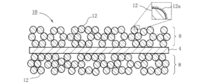
- FIG. 2 is a diagram schematically showing a bonding sheet in which porous preform layers are formed on both sides of a copper sheet according to the present embodiment
- FIG. 2 is a diagram showing a situation in which a porous preform layer is formed on one side of a substrate whose surface is made of copper or nickel by the electrolytic copper plating method of the present embodiment.
- 1 is a schematic diagram of a bonding substrate having a porous preform layer formed on one side of the substrate
- FIG. FIG. 4 is a diagram showing a first method for manufacturing a joined body using the joining sheet of the present embodiment
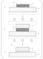
- FIGS. 5(a) to 5(d) are diagrams showing steps of forming a preform layer on a part of a substrate by electrolytic copper plating to manufacture a bonding substrate.
- FIGS. 5(a) to 5(d) are diagrams showing steps of forming a preform layer on a part of a substrate by electrolytic copper plating to manufacture a bonding substrate.
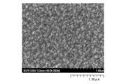
- FIG. 2 is a scanning electron micrograph of the preform layer of Example 1 of the present invention taken at a magnification of 50,000 times.
- FIG. 2 is a scanning electron micrograph of the preform layer of Example 1 of the present invention taken at a magnification of 100,000 times.
- the acidic electrolytic copper plating solution of the present embodiment comprises a soluble copper salt and copper ion electrodeposition having 2 or more and 3 or less nitrogen atoms in the five-membered ring represented by the above formulas (1) to (4). It contains an azole compound that is an inhibitor, an acid, and water. Any bath solution can be used as long as it contains these components. Brighteners, surfactants, antioxidants and the like can be added as required.
- soluble copper salts include copper sulfate, copper oxide, and copper carbonate; copper alkanesulfonates such as copper methanesulfonate and copper propanoate; copper alkanolsulfonates such as copper isethionate and copper propanolsulfonate; , organic acids such as copper citrate and copper tartrate. These can be used singly or in combination of two or more.
- acids include organic acids and inorganic acids.
- specific examples of acids include sulfuric acid; alkanesulfonic acids such as methanesulfonic acid and propanesulfonic acid; alkanolsulfonic acids such as isethionic acid and propanolsulfonic acid; and organic acids such as citric acid, tartaric acid and formic acid. These can be used singly or in combination of two or more.
- Water includes pure water such as ion-exchanged water and distilled water.
- the azole compound which is a copper ion electrodeposition inhibitor having 2 or more and 3 or less nitrogen atoms in the five-membered ring, will be described.
- Specific examples of the azole compounds represented by the above formulas (1) to (4) include imidazole, 2-aminoimidazole, pyrazole, 3-aminoimidazole, 1,2,3-triazole, 1,2,4- triazole, 3-amino-1,2,4-triazole, 3,5-diamino-1,2,4-triazole, 3-amino-5-methylthio-1H-1,2,4-triazole and the like.
- the imidazole is a kind of azole compound represented by the above formula (1), and is represented by the following formula (5).
- 2-Aminoimidazole is one of the azole compounds represented by the above formula (1), and is represented by the following formula (6).
- Pyrazole is one of the azole compounds represented by the above formula (2), and is represented by the following formula (7).
- 3-Aminoimidazole is one of the azole compounds represented by the above formula (2), and is represented by the following formula (8).
- 1,2,3-triazole is one of the azole compounds represented by the above formula (3) and is represented by the following formula (9).
- 1,2,4-triazole is a kind of azole compound represented by the above formula (4), and is represented by the following formula (10).
- 3-Amino-1,2,4-triazole is one of the azole compounds represented by the above formula (4), and is represented by the following formula (11).
- 3,5-diamino-1,2,4-triazole is one of the azole compounds represented by the above formula (4) and is represented by the following formula (12).
- 3-amino-5-methylthio-1H-1,2,4-triazole is one of the azole compounds represented by formula (4) above, and represented by formula (13) below.
- the acidic electrolytic copper plating solution of the present embodiment comprises the soluble copper salt, the azole compound having 2 or more and 3 or less nitrogen atoms in the five-membered ring which is the copper ion electrodeposition inhibitor described above, an acid, It can be prepared by mixing with water.
- the concentration of the soluble copper salt is 0.1 mol/L or more, preferably 0.1 mol/L or more and 1.0 mol/L or less. If the concentration of the soluble copper salt is less than 0.1 mol/L, a preform layer as a copper plating film cannot be formed.
- the concentration of the azole compound, which is a copper ion electrodeposition inhibitor is 10 mmol/L or more and 50 mmol/L or less, preferably 10 mmol/L or more and 30 mmol/L or less.
- the concentration of the azole compound is less than 10 mmol/L, the effect of suppressing the electrodeposition of copper ions is poor, and the preform layer as the copper plating film does not become porous.
- the concentration of the azole compound exceeds 50 mmol/L, the electrodeposition of copper ions is excessively suppressed, the copper plating film becomes brittle, and the strength is remarkably deteriorated.
- the azole compound cannot be dissolved in the liquid and precipitates.
- the concentration of the acid but pH 0-5 is preferred, and pH 1-3 is more preferred.
- the chloride ion concentration is 10 ppm or less, preferably 5 ppm or less. When the chloride ion concentration exceeds 10 ppm, the chloride ions are adsorbed on the copper surface and inhibit the formation of the preform layer as the copper plating film.
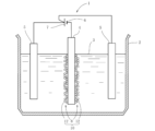
- a plating tank 2 of an electrolytic copper plating apparatus 1 is filled with the acidic electrolytic copper plating solution 3 described above.
- Two copper materials 5, 5 made of electrolytic copper or oxygen-free copper are arranged so as to face each other on both sides of 4.
- a copper sheet 4 serves as a cathode and is connected to a cathode 6, and two copper materials 5, 5 serve as soluble anodes and are connected to an anode 7.
- FIG. By applying a voltage to the copper sheet 4 and the copper materials 5 , preform layers 8 are formed as copper plating films on both sides of the copper sheet 4 .
- the copper sheet 4 is a copper foil, and the thickness of the copper sheet 4 is exaggerated in FIG.
- Pure copper or a copper alloy can be used as the copper foil forming the copper sheet 4 .
- oxygen-free copper, tough pitch copper, phosphorus-deoxidized copper, or the like can be used.
- the copper foil a rolled copper foil obtained by rolling such a copper material can be used, or an electrolytic copper foil or the like produced by an electrolytic copper plating method can be used.
- the copper material 5 is used as the soluble anode here, it is also possible to use an insoluble anode such as Pt/Ti instead of the copper material 5 .
- a bonding sheet having a preform layer on one side of the copper sheet 4 can be manufactured by placing the copper material 5 on only one side of the copper sheet 4 .
- FIG. 3A Another electrolytic copper plating method is shown in FIG. 3A.
- a substrate 4a having a surface made of copper or nickel is placed in an acidic electrolytic copper plating solution 3 of an electrolytic copper plating apparatus 1, and a copper material 5 is placed so as to face one side of the substrate 4a. are arranged, and electrolytic copper plating is performed in the same manner as the electrolytic copper plating shown in FIG.
- a resist film 4b is formed in advance on the surface of the substrate 4a so as to have openings at predetermined intervals.
- a porous preform layer 8 containing copper particles 12 is formed as a copper plating film in the openings of the resist film 4b formed on one side of the substrate 4a.
- the azole compound which is a copper ion electrodeposition inhibitor
- the cathode surface which is the surface of the copper sheet 4 or the substrate 4a, together with the copper ions.
- Electrodeposition of copper ions is strongly suppressed by the presence of the azole compound, copper nucleation is given priority, and a porous preform layer 8 containing copper particles 12 is formed as a copper plating film on the cathode surface.
- a washing solvent such as ethanol, water or acetone
- the thickness of the porous preform layer 8 of the copper sheet 4 or substrate 4a is preferably 15 ⁇ m to 50 ⁇ m. If the thickness of the preform layer is less than 15 ⁇ m, the strength of the preform layer itself is lowered, making it difficult to handle. If the thickness of the preform layer exceeds 50 ⁇ m, it is difficult for the preform layer to conform to irregularities on the surfaces of the base material or the electronic component, which will be described later, during bonding, and the bonding strength of the bonded body may decrease.
- the total thickness of the joining sheet 10 thus obtained is 25 ⁇ m at the thinnest. That is, it is 25 ⁇ m or more.
- a preferred total thickness is between 25 ⁇ m and 140 ⁇ m. If the total thickness is less than the lower limit of 25 ⁇ m, the strength of the bonding sheet itself may decrease. If the total thickness exceeds 140 ⁇ m, if the base material is a substrate and the substrate to which the electronic component is to be bonded is warped, there is a possibility that the warpage cannot be absorbed.
- the total thickness of the bonding sheet is measured as follows. The bonding sheet is completely covered with epoxy resin, then cut perpendicular to the surface of the bonding sheet, and the cut surface is polished with an argon ion beam. Then, the polished processed surface is observed with an SEM (scanning electron microscope), the thickness of the bonding sheet is randomly measured at 100 or more locations, and the average value is taken as the thickness of the bonding sheet.
- a bonding sheet 10 having porous preform layers 8 formed on both sides of a copper sheet 4 shown in FIG. 2 will be described in detail.
- the porous preform layer 8 is formed in the form of an aggregate of copper particles 12 in which the copper particles 12 are stacked on both sides of the copper sheet 4 .
- the preform layer 8 containing the copper particles 12 has an average porosity of 11% or more and 78% or less. If the average porosity is less than 11%, less copper particles 12 contribute to sintering of the porous preform layer 8, and the sinterability of the copper particles 12 is lowered.
- the average porosity of the preform layer 8 is preferably 11% or more and 17% or less.
- the porous preform layer 8 is composed of the copper particles 12 and the copper nanoparticles 12 a coated on the surfaces of the copper particles 12 .
- the electrodeposition of copper is suppressed, nucleation is prioritized, and the surface of the copper particles 12 Copper nanoparticles 12a are formed. Due to such a characteristic structure, when the porous preform layer 8 is pressed, the copper particles 12 are easily sintered to easily form a strong bonding layer.
- the average particle size of the copper nanoparticles 12a calculated from the BET measurement value is 9.59 nm or more and 850 nm or less. If the average particle diameter of the copper nanoparticles 12a is out of this range, the copper particles 12 are difficult to sinter easily.
- a preferable range of the average particle size of the copper nanoparticles 12a is 50 nm or more and 300 nm or less.
- the average porosity of the preform layer 8 described above is calculated by image analysis of the cross section of the preform layer 8 with a scanning electron microscope. Let the arithmetic mean of the porosity (P) calculated
- required by following formula (A) be average porosity. Specifically, images are taken three times in different fields of view, and the average value of the calculated porosities is used as the average porosity. P (%) ( S2 / S1 ) x 100 (A) However, in the formula (A), P is the porosity of the preform layer 8, S1 is the total area of the preform layer 8, and S2 is the area of the voids in the preform layer 8. .
- the average particle size of the copper nanoparticles 12a described above is calculated from the specific surface area of the porous preform layer 8 measured by the BET method. Measurement by the BET method is performed using HM-model-1201 manufactured by Macsorb. The copper sheet 4 with the preform layer 8 is cut into 2 mm squares, filled in a measurement cell, and the specific surface area is measured by the BET one-point method. The mass of the copper sheet 4 is subtracted from the measured value, and the mass of the preform layer 8 itself is converted. From the calculated BET measurement value, the particle size of the copper nanoparticles 12a is calculated based on the following formula (B).
- the coefficient 335.95 in the following formula (B) is a value calculated from the theoretical values of the density of copper, the surface area of the copper nanoparticles 12a, and the volume of the copper nanoparticles 12a.
- a first method for manufacturing a bonded body using the bonding sheet 10 will be described. As shown in FIG. 4(a), first, as the substrate 16, an oxygen-free copper plate, various heat dissipation substrates, FR4 (Flame Retardant Type 4) substrates, kovar substrates, etc. are prepared, and as the electronic component 17, a silicon chip is prepared. Electronic parts such as elements and LED chip elements are prepared. Next, the bonding sheet 10 is arranged at a predetermined position on the base material 16, and the electronic component 17 is arranged on the bonding sheet 10 as shown in FIG. 4(b).
- a bonded body 44 is formed using a bonding substrate 40 having a porous preform layer 8 formed on the surface of a substrate 46 .
- the porous preform layer 8 shown in FIG. 5 is the same as the porous preform layer 8 shown in FIG.
- the substrate 46 has a substrate surface made of copper or nickel.
- the substrate 46 is an oxygen-free copper plate, a Si substrate having a copper metallized surface, or an oxygen-free copper plate having a Ni plating layer on the substrate surface.
- Electronic component 47 shown in FIG. 5 is the same as electronic component 17 shown in FIG.
- a substrate 46 whose surface is made of copper or nickel is prepared.
- the surface of the substrate 46 is masked with a resist film 41 and patterned so as to have openings 46a at predetermined intervals.
- it is placed in the acidic electrolytic copper plating solution 3 described above to carry out electrolytic copper plating to form a porous preform layer 8 on the opening 46a as shown in FIG. 5(c).
- a bonding substrate 40 having a porous preform layer 8 formed on a substrate 46 is produced.
- This electrolytic copper plating can be performed by the method described above.
- the preform layer 8 is formed only on the opening 46a, but the preform layer 8 may be formed on the entire surface of the substrate 46 without providing the resist film 41.
- an electronic component 47 is bonded onto the porous preform layer 8 of the bonding substrate 40 .
- the bonding substrate 40 having the porous preform layer 8 formed thereon is placed on the pressure plate 42 .
- an electronic component 47 is placed on the preform layer 8 to obtain a laminate.
- the pressure plate 42 and the pressure plate 43 heat the laminated body composed of the bonding substrate 40 and the electronic component 47 while applying pressure in the lamination direction.
- the pressurizing and heating conditions are the same as the pressurizing and heating conditions for the substrate 16 and the electronic component 17 shown in FIG. 4(a).
- the preform layer 8 serves as a bonding layer 45 to bond the bonding substrate 40 and the electronic component 47 to obtain a bonded body 44 .
- the substrate is an oxygen-free copper plate on which no preform layer is formed, or a substrate having a copper metallized bonding surface is prepared.
- a preform layer may be formed in advance.
- a preform layer may be formed on the substrate and then on the bonding surface of the electronic component. By forming preform layers on both sides, the bonding strength between the substrate and the electronic component can be further increased, which is preferable.
- Table 1 shows the types, structural formulas, and compound names of copper ion electrodeposition inhibitors used in Examples 1 to 20 and Comparative Examples 1 to 10.
- a Si wafer (thickness: 1.2 mm) having a copper layer with a thickness of about 500 nm formed on the surface thereof by a sputtering method was used.
- the surface of the Si wafer having this copper layer (hereinafter simply referred to as the Si wafer) was patterned with a photoresist so that one die (15 mm square) had 6002 perfectly circular openings with a diameter of 75 ⁇ m.
- the Si wafer Prior to the electrolytic copper plating of the Si wafer, the Si wafer was hydrophilized with a plasma cleaner.
- the Si wafer was pre-wet with pure water, then immersed in an aqueous solution of sulfuric acid having a concentration of 10% by mass, and washed with an acid.
- the acid-cleaned Si wafer was washed with water.
- Electrolytic copper plating was performed on one surface (pattern surface) of the Si wafer using the plating apparatus 1 shown in FIG. 3A containing the copper plating solution shown below.
- a copper plating bath was prepared with the following liquid composition. Plating conditions are also shown. Table 2 below shows characteristic items among the composition of the plating bath and the plating conditions of Example 1. In Example 1, no. The 3,5-diamino-1,2,4-triazole of formula (12) described above in 8 was used.
- Copper sulfate pentahydrate (as Cu 2+ ): 0.1 mol/L Copper ion electrodeposition inhibitor (3,5-diamino-1,2,4-triazole): 10 mmol/L Chloride ion: 0 ppm
- Deionized water balance [plating conditions] Bath temperature: 26°C Bath pH: 2.5 Cathode current density: 0.4 A/dm 2
- FIG. 1 A porous preform layer made of copper particles was formed on the Si wafer by immersing the Si wafer in the above copper plating solution and performing electrolytic copper plating under the above plating conditions.
- 6A and 6B show scanning electron micrographs of the surface of the preform layer of Example 1.
- Examples 2 to 20 and Comparative Examples 4 to 10 any one of the concentration of copper sulfate pentahydrate, the type of copper ion electrolytic deposition inhibitor, the concentration of the copper ion electrolytic inhibitor, and the chloride ion concentration was carried out. Same as Example 1 or modified. Also, the cathode current density during plating was the same as in Example 1 or changed. Otherwise, electrolytic copper plating was performed in the same manner as in Example 1.
- characteristic items are shown in Table 2 above and Table 3 below, respectively.
- Comparative Example 1 In Comparative Example 1, the concentration of copper sulfate pentahydrate was 1.0 mol/L, the cathode current density during plating was 3.0 A/dm 2 , and copper was plated onto the Si wafer in the same manner as in Example 1. did In Comparative Example 1, no copper ion electrodeposition inhibitor was used. The chloride ion concentration in the copper plating solution was 80 ppm.
- Comparative Example 2 In Comparative Example 2, the concentration of copper sulfate pentahydrate was 1.0 mol/L, the cathode current density during plating was 3.0 A/dm 2 , and copper was plated onto the Si wafer in the same manner as in Example 1. did In Comparative Example 1, no copper ion electrodeposition inhibitor was used. The chloride ion concentration in the copper plating solution was 5 ppm.
- Comparative Example 3 In Comparative Example 3, the concentration of copper sulfate pentahydrate was 1.0 mol/L, the cathode current density during plating was 3.0 A/dm 2 , and copper was plated onto the Si wafer in the same manner as in Example 1. did In Comparative Example 3, 50 ppm of 3,3-dithiobis(1-propanesulfonic acid) disodium and polyethylene glycol (Mw: 3400) were used as copper ion electrodeposition inhibitors for comparison with organic compounds other than azole compounds. A common additive containing 300 ppm of was used. The chloride ion concentration in the copper plating solution was 80 ppm.
- chips 47 are arranged on the preform layers 8 of the 25 types of bonding substrates 40 obtained in Examples 1 to 20 and Comparative Examples 1 to 5, and the As shown in (g), a joined body 44 was obtained by heating while pressurizing.
- the chip 47 is composed of a 2.5 mm square Si wafer (thickness: 1.2 mm) with copper metallization on the outermost surface.
- This bonding was carried out by using a pressure heating bonding apparatus (manufactured by Alpha Design; HTB-MM) under a nitrogen atmosphere at a temperature of 300° C. and a pressure of 30 MPa for 30 minutes.
- the shear strength of 25 types of conjugates was measured as follows.
- the shear strength of the bonded body was measured using a shear strength evaluation tester (bond tester manufactured by Nordson Advanced Technologies; Dage Series 4000). Specifically, the shear strength was measured by horizontally fixing the Si wafer, which is the substrate of the bonded body, and pressing the chip horizontally with a shear tool at a position 50 ⁇ m above the surface (upper surface) of the bonding layer. , by measuring the strength when the chip breaks. In addition, the moving speed of the share tool was set to 0.1 mm/sec. The strength test was performed three times per condition, and the arithmetic mean value of the obtained values was used as the measurement value of the bonding strength.
- Tables 2 and 3 above show the shear strength of the 25 types of bonded bodies. If the bonding strength was 15 MPa or more, it was judged as “good”; In addition, "-" in the bonding strength in Tables 2 and 3 indicates that the chip 47 and the bonding substrate 40 were attempted to be bonded but were not bonded, or the chip 47 was peeled off before the bonding strength was measured. It means messed up. The results are shown in Tables 2 and 3 above.
- Comparative Examples 1 and 2 did not contain a copper ion electrodeposition inhibitor having a function of forming a porous copper plating film. Moreover, in Comparative Example 3, the copper ion electrodeposition inhibitor added did not have the function of forming a porous copper plating film. Therefore, in Comparative Examples 1 to 3, a copper plating film was formed, but the average porosity was "0%” and the copper plating film was not porous. For this reason, in Comparative Examples 1 and 2, the chip and the bonding substrate were not bonded, and the judgment was "defective" in both cases. In Comparative Example 3, the bonding strength was as low as "12.4 MPa", and the judgment was "slightly unsatisfactory".
- the concentration of copper ions was as low as “0.01 mol / L”, so sufficient electrodeposition was not performed, the average porosity was as low as “8%”, and the average particle size of the copper nanoparticles was It was 42 nm and was a preform layer with a low degree of porosity as a copper plating film. Therefore, the bonding strength was as low as "9.2 MPa", and the judgment was "slightly unsatisfactory".
- the average particle diameter calculated from the average porosity of the preform layer and the BET value was appropriately controlled, and the average pore size of the preform layer formed on the Si wafer was degree is within the above-mentioned range of 11% or more and 78% or less, and the average particle size of the copper nanoparticles calculated from the BET value is also within the above-mentioned range of 9.59 nm to 850 nm.
- the acidic electrolytic copper plating solution of the present embodiment can be used in the process of forming a porous preform layer for joining two members in the assembly and mounting of electronic parts.
Landscapes
- Chemical & Material Sciences (AREA)
- Engineering & Computer Science (AREA)
- Chemical Kinetics & Catalysis (AREA)
- Electrochemistry (AREA)
- Materials Engineering (AREA)
- Metallurgy (AREA)
- Organic Chemistry (AREA)
- Automation & Control Theory (AREA)
- Electroplating Methods And Accessories (AREA)
- Electroplating And Plating Baths Therefor (AREA)
Priority Applications (2)
| Application Number | Priority Date | Filing Date | Title |
|---|---|---|---|
| US18/705,691 US20250003102A1 (en) | 2021-11-08 | 2022-11-08 | Acidic electrolytic copper plating liquid, method for forming preform layer, method for producing joining sheet, method for producing joining substrate, and method for producing joined body |
| KR1020247012921A KR20240110560A (ko) | 2021-11-08 | 2022-11-08 | 산성 전해 구리 도금액, 프리폼층의 형성 방법, 접합용 시트의 제조 방법, 접합용 기판의 제조 방법 및 접합체의 제조 방법 |
Applications Claiming Priority (2)
| Application Number | Priority Date | Filing Date | Title |
|---|---|---|---|
| JP2021-181970 | 2021-11-08 | ||
| JP2021181970A JP2023069822A (ja) | 2021-11-08 | 2021-11-08 | 酸性電解銅めっき液、プリフォーム層の形成方法、接合用シートの製造方法、接合用基板の製造方法及び接合体の製造方法 |
Publications (1)
| Publication Number | Publication Date |
|---|---|
| WO2023080250A1 true WO2023080250A1 (ja) | 2023-05-11 |
Family
ID=86241621
Family Applications (1)
| Application Number | Title | Priority Date | Filing Date |
|---|---|---|---|
| PCT/JP2022/041470 Ceased WO2023080250A1 (ja) | 2021-11-08 | 2022-11-08 | 酸性電解銅めっき液、プリフォーム層の形成方法、接合用シートの製造方法、接合用基板の製造方法及び接合体の製造方法 |
Country Status (5)
| Country | Link |
|---|---|
| US (1) | US20250003102A1 (https=) |
| JP (1) | JP2023069822A (https=) |
| KR (1) | KR20240110560A (https=) |
| TW (1) | TW202340541A (https=) |
| WO (1) | WO2023080250A1 (https=) |
Families Citing this family (2)
| Publication number | Priority date | Publication date | Assignee | Title |
|---|---|---|---|---|
| CN121942350A (zh) * | 2023-09-28 | 2026-04-28 | 古河电气工业株式会社 | 接合用膜、半导体模块、逆变器、电子设备以及半导体模块的制造方法 |
| JP2025137155A (ja) * | 2024-03-08 | 2025-09-19 | 三菱マテリアル株式会社 | 酸性電解銅めっき液 |
Citations (5)
| Publication number | Priority date | Publication date | Assignee | Title |
|---|---|---|---|---|
| JP2001152387A (ja) * | 1999-09-16 | 2001-06-05 | Ishihara Chem Co Ltd | ボイドフリー銅メッキ方法 |
| JP2010121194A (ja) * | 2008-11-21 | 2010-06-03 | Okuno Chem Ind Co Ltd | 多孔質めっき皮膜形成用添加剤及び多孔質めっき皮膜の形成方法 |
| JP2015533946A (ja) * | 2012-09-24 | 2015-11-26 | アルスィメール | 電解液及びバリア層上に銅を電気めっきする方法 |
| JP2017020082A (ja) * | 2015-07-13 | 2017-01-26 | 株式会社Jcu | 多孔質壺状銅めっき皮膜形成用電気めっき浴およびこれを用いた多孔質壺状銅めっき皮膜の形成方法 |
| WO2020040120A1 (ja) * | 2018-08-23 | 2020-02-27 | Dic株式会社 | 積層体、成形品、導電性パターン及び電子回路 |
-
2021
- 2021-11-08 JP JP2021181970A patent/JP2023069822A/ja active Pending
-
2022
- 2022-11-08 KR KR1020247012921A patent/KR20240110560A/ko active Pending
- 2022-11-08 WO PCT/JP2022/041470 patent/WO2023080250A1/ja not_active Ceased
- 2022-11-08 US US18/705,691 patent/US20250003102A1/en active Pending
- 2022-11-08 TW TW111142603A patent/TW202340541A/zh unknown
Patent Citations (5)
| Publication number | Priority date | Publication date | Assignee | Title |
|---|---|---|---|---|
| JP2001152387A (ja) * | 1999-09-16 | 2001-06-05 | Ishihara Chem Co Ltd | ボイドフリー銅メッキ方法 |
| JP2010121194A (ja) * | 2008-11-21 | 2010-06-03 | Okuno Chem Ind Co Ltd | 多孔質めっき皮膜形成用添加剤及び多孔質めっき皮膜の形成方法 |
| JP2015533946A (ja) * | 2012-09-24 | 2015-11-26 | アルスィメール | 電解液及びバリア層上に銅を電気めっきする方法 |
| JP2017020082A (ja) * | 2015-07-13 | 2017-01-26 | 株式会社Jcu | 多孔質壺状銅めっき皮膜形成用電気めっき浴およびこれを用いた多孔質壺状銅めっき皮膜の形成方法 |
| WO2020040120A1 (ja) * | 2018-08-23 | 2020-02-27 | Dic株式会社 | 積層体、成形品、導電性パターン及び電子回路 |
Also Published As
| Publication number | Publication date |
|---|---|
| KR20240110560A (ko) | 2024-07-15 |
| JP2023069822A (ja) | 2023-05-18 |
| TW202340541A (zh) | 2023-10-16 |
| US20250003102A1 (en) | 2025-01-02 |
Similar Documents
| Publication | Publication Date | Title |
|---|---|---|
| JP5859155B1 (ja) | 複合金属箔及びその製造方法並びにプリント配線板 | |
| KR101298999B1 (ko) | 미세회로 형성을 위한 임베디드용 동박 | |
| WO2023080250A1 (ja) | 酸性電解銅めっき液、プリフォーム層の形成方法、接合用シートの製造方法、接合用基板の製造方法及び接合体の製造方法 | |
| KR20120055719A (ko) | 반도체 칩 탑재용 기판 및 그의 제조 방법 | |
| WO2020031721A1 (ja) | 粗化処理銅箔、キャリア付銅箔、銅張積層板及びプリント配線板 | |
| US20240300215A1 (en) | Bonding sheet with preform layer, method for manufacturing bonded body, and to-be-bonded member with preform layer | |
| WO2022202539A1 (ja) | キャリア付銅箔、銅張積層板及びプリント配線板 | |
| JP7748116B2 (ja) | 金属箔、それを備えた金属箔を有するキャリア、及びそれを含むプリント回路基板 | |
| TWI598005B (zh) | 厚銅層與其形成方法 | |
| CN108464062B (zh) | 印刷电路板的制造方法 | |
| JP7826882B2 (ja) | Cuピラーの接合方法、および、Cuピラー接合体の製造方法 | |
| Nakagawa et al. | Investigation of Cu-Cu direct bonding process utilized by high porosity and nanocrystal structure | |
| CN100572608C (zh) | 铜箔的粗面化处理方法以及粗面化处理液 | |
| JP2023168651A (ja) | 銅-亜鉛合金電気めっき液、銅-亜鉛合金バンプの形成方法、ナノポーラス銅バンプの形成方法、銅-亜鉛合金バンプ付き基材及びナノポーラス銅バンプ付き基材 | |
| CN113646469A (zh) | 印刷电路板用金属箔、带载体的金属箔和覆金属层叠板、及使用其的印刷电路板的制造方法 | |
| US6117566A (en) | Lead frame material | |
| CN103003473A (zh) | 刻蚀铜和铜合金的方法 | |
| CN118308765A (zh) | 一种用于盲孔填充柱状纳米孪晶铜的电镀液及其应用 | |
| JP2013093360A (ja) | 半導体チップ搭載用基板及びその製造方法 | |
| TWI917085B (zh) | 印刷配線板之製造方法 | |
| TW202536980A (zh) | Cu柱之接合方法及Cu柱接合體之製造方法 | |
| JP2025137155A (ja) | 酸性電解銅めっき液 | |
| KR102686710B1 (ko) | 표면조도가 낮은 금속박을 이용한 기판의 회로패턴 형성방법 | |
| TW202540499A (zh) | 印刷配線板之製造方法 | |
| WO2025186942A1 (ja) | Cuピラーの接合方法、および、Cuピラー接合体の製造方法 |
Legal Events
| Date | Code | Title | Description |
|---|---|---|---|
| 121 | Ep: the epo has been informed by wipo that ep was designated in this application |
Ref document number: 22890070 Country of ref document: EP Kind code of ref document: A1 |
|
| WWE | Wipo information: entry into national phase |
Ref document number: 18705691 Country of ref document: US |
|
| 122 | Ep: pct application non-entry in european phase |
Ref document number: 22890070 Country of ref document: EP Kind code of ref document: A1 |