WO2023079863A1 - 半導体記憶装置 - Google Patents
半導体記憶装置 Download PDFInfo
- Publication number
- WO2023079863A1 WO2023079863A1 PCT/JP2022/036022 JP2022036022W WO2023079863A1 WO 2023079863 A1 WO2023079863 A1 WO 2023079863A1 JP 2022036022 W JP2022036022 W JP 2022036022W WO 2023079863 A1 WO2023079863 A1 WO 2023079863A1
- Authority
- WO
- WIPO (PCT)
- Prior art keywords
- voltage
- bit line
- supply line
- transistor
- read
- Prior art date
- Legal status (The legal status is an assumption and is not a legal conclusion. Google has not performed a legal analysis and makes no representation as to the accuracy of the status listed.)
- Ceased
Links
Images








Classifications
-
- G—PHYSICS
- G11—INFORMATION STORAGE
- G11C—STATIC STORES
- G11C13/00—Digital stores characterised by the use of storage elements not covered by groups G11C11/00, G11C23/00, or G11C25/00
- G11C13/0002—Digital stores characterised by the use of storage elements not covered by groups G11C11/00, G11C23/00, or G11C25/00 using resistive RAM [RRAM] elements
- G11C13/0021—Auxiliary circuits
- G11C13/0061—Timing circuits or methods
-
- G—PHYSICS
- G11—INFORMATION STORAGE
- G11C—STATIC STORES
- G11C11/00—Digital stores characterised by the use of particular electric or magnetic storage elements; Storage elements therefor
- G11C11/02—Digital stores characterised by the use of particular electric or magnetic storage elements; Storage elements therefor using magnetic elements
- G11C11/16—Digital stores characterised by the use of particular electric or magnetic storage elements; Storage elements therefor using magnetic elements using elements in which the storage effect is based on magnetic spin effect
- G11C11/165—Auxiliary circuits
- G11C11/1659—Cell access
-
- G—PHYSICS
- G11—INFORMATION STORAGE
- G11C—STATIC STORES
- G11C11/00—Digital stores characterised by the use of particular electric or magnetic storage elements; Storage elements therefor
- G11C11/02—Digital stores characterised by the use of particular electric or magnetic storage elements; Storage elements therefor using magnetic elements
- G11C11/16—Digital stores characterised by the use of particular electric or magnetic storage elements; Storage elements therefor using magnetic elements using elements in which the storage effect is based on magnetic spin effect
- G11C11/165—Auxiliary circuits
- G11C11/1673—Reading or sensing circuits or methods
-
- G—PHYSICS
- G11—INFORMATION STORAGE
- G11C—STATIC STORES
- G11C13/00—Digital stores characterised by the use of storage elements not covered by groups G11C11/00, G11C23/00, or G11C25/00
- G11C13/0002—Digital stores characterised by the use of storage elements not covered by groups G11C11/00, G11C23/00, or G11C25/00 using resistive RAM [RRAM] elements
- G11C13/0021—Auxiliary circuits
- G11C13/0038—Power supply circuits
-
- G—PHYSICS
- G11—INFORMATION STORAGE
- G11C—STATIC STORES
- G11C13/00—Digital stores characterised by the use of storage elements not covered by groups G11C11/00, G11C23/00, or G11C25/00
- G11C13/0002—Digital stores characterised by the use of storage elements not covered by groups G11C11/00, G11C23/00, or G11C25/00 using resistive RAM [RRAM] elements
- G11C13/0021—Auxiliary circuits
- G11C13/004—Reading or sensing circuits or methods
-
- G—PHYSICS
- G11—INFORMATION STORAGE
- G11C—STATIC STORES
- G11C17/00—Read-only memories programmable only once; Semi-permanent stores, e.g. manually-replaceable information cards
- G11C17/14—Read-only memories programmable only once; Semi-permanent stores, e.g. manually-replaceable information cards in which contents are determined by selectively establishing, breaking or modifying connecting links by permanently altering the state of coupling elements, e.g. PROM
- G11C17/16—Read-only memories programmable only once; Semi-permanent stores, e.g. manually-replaceable information cards in which contents are determined by selectively establishing, breaking or modifying connecting links by permanently altering the state of coupling elements, e.g. PROM using electrically-fusible links
-
- G—PHYSICS
- G11—INFORMATION STORAGE
- G11C—STATIC STORES
- G11C17/00—Read-only memories programmable only once; Semi-permanent stores, e.g. manually-replaceable information cards
- G11C17/14—Read-only memories programmable only once; Semi-permanent stores, e.g. manually-replaceable information cards in which contents are determined by selectively establishing, breaking or modifying connecting links by permanently altering the state of coupling elements, e.g. PROM
- G11C17/18—Auxiliary circuits, e.g. for writing into memory
-
- G—PHYSICS
- G11—INFORMATION STORAGE
- G11C—STATIC STORES
- G11C7/00—Arrangements for writing information into, or reading information out from, a digital store
- G11C7/14—Dummy cell management; Sense reference voltage generators
-
- G—PHYSICS
- G11—INFORMATION STORAGE
- G11C—STATIC STORES
- G11C13/00—Digital stores characterised by the use of storage elements not covered by groups G11C11/00, G11C23/00, or G11C25/00
- G11C13/0002—Digital stores characterised by the use of storage elements not covered by groups G11C11/00, G11C23/00, or G11C25/00 using resistive RAM [RRAM] elements
- G11C13/0021—Auxiliary circuits
- G11C13/004—Reading or sensing circuits or methods
- G11C2013/0054—Read is performed on a reference element, e.g. cell, and the reference sensed value is used to compare the sensed value of the selected cell
Definitions
- An embodiment according to the present disclosure relates to a semiconductor memory device.
- a resistance change memory element and a fuse element are known as representative memory elements whose resistance value changes according to the flowing current.
- a resistance change memory element is a memory device that utilizes the input/output of conductive ions to an insulating film, the change in conductivity according to the magnetization direction of a magnetic film, or the phase change in the crystal structure. can change the resistance value.
- a fuse element made of polysilicon is electrically blown to control its resistance value (see, for example, Non-Patent Document 1). reference).
- a fuse element there is known one that stores data by whether or not a gate oxide film of a MOS transistor is electrically broken down.
- electrically controllable fuse elements are specifically referred to as electrical fuses (eFUSEs).
- the present disclosure provides a semiconductor memory device that can more appropriately perform read operations.
- one or more first memory cells connected in parallel between a first voltage supply line supplying a first voltage and a second voltage supply line supplying a second voltage different from the first voltage; , one or more second memory cells connected in parallel between the second voltage supply line and a third voltage supply line supplying the first voltage; with each of the first memory cells, a first storage element having a resistance value corresponding to the first state or the second state; a first cell transistor connected between the first memory element and the first voltage supply line; each of the second memory cells, a second storage element having a resistance value corresponding to the first state or the second state; and a second cell transistor connected between the second memory element and the third voltage supply line.
- the number of the first memory cells and the number of the second memory cells may be the same.
- the first memory cell and the second memory cell may be arranged substantially symmetrically with the second voltage supply line interposed therebetween.
- the first voltage is supplied to the first voltage supply line and the third voltage supply line, and the second voltage is supplied to the second voltage supply line.
- a voltage supply unit for stopping the supply of the first voltage A cell transistor that turns on the first cell transistor of the first memory cell to be read or the second cell transistor of the second memory cell to be read while the supply of the first voltage is stopped.
- a control unit may be further provided.
- the potential difference between the first voltage and the second voltage is the first voltage supply line and the third voltage supply line after the cell transistor control unit turns on the first cell transistor or the second cell transistor. It may be a potential difference according to the difference in voltage change rate between and.
- the second voltage supply line may be fixed to the second voltage.
- the first storage element and the second storage element having a resistance value generate a reference voltage having a voltage level between a voltage generated by being biased based on the first voltage and the second voltage.
- a reference voltage generator; a comparison unit that compares the reference voltage with a voltage generated by biasing the first memory element or the second memory element based on the first voltage and the second voltage; may be further provided.
- the reference voltage generation unit a first reference voltage generator connected between the first voltage supply line and the second voltage supply line and configured to generate the reference voltage when a read operation of the second memory cell is performed; a second reference voltage generator connected between the second voltage supply line and the third voltage supply line for generating the reference voltage when a read operation of the first memory cell is performed; may have
- the first reference voltage generator and the second reference voltage generator may be arranged substantially symmetrically with the second voltage supply line interposed therebetween.
- the first reference voltage generation unit a first reference resistance element; a first reference transistor connected between the first reference resistance element and the first voltage supply line; has The second reference voltage generation unit a second reference resistance element; a second reference transistor connected between the second reference resistance element and the third voltage supply line; may have
- the comparison unit compares the voltage of the first voltage supply line and the voltage of the third voltage supply line to determine whether the reference voltage and the first memory element or the second memory element are the same as the first memory element. comparing one voltage and a voltage generated biased based on the second voltage; A comparison control unit may be further provided that causes the comparison unit to start comparison at timing according to the voltages of the first voltage supply line and the third voltage supply line.
- the comparison control unit is When the first voltage is higher than the second voltage, the comparing unit performs comparison at timing when the voltage of at least one of the first voltage supply line and the third voltage supply line becomes lower than a first predetermined value. let it start When the first voltage is lower than the second voltage, the comparing unit performs the comparison at the timing when the voltage of at least one of the first voltage supply line and the third voltage supply line becomes higher than a second predetermined value. You can start.
- the first voltage may be higher than the second voltage.
- the first voltage is lower than the second voltage
- the second voltage in a write operation may be higher than the first voltage in a read operation.
- the first voltage in a write operation, is higher than the second voltage;
- the first voltage in a write operation may be higher than the first voltage in a read operation.
- the first voltage may be lower than the second voltage.
- the first voltage is lower than the second voltage
- the second voltage in a write operation may be higher than the second voltage in a read operation.
- FIG. 1 is a schematic diagram showing a configuration example of a semiconductor memory device according to a first embodiment
- FIG. 1 is a circuit diagram showing a detailed configuration example of a semiconductor memory device according to a first embodiment
- FIG. 4 is a timing chart showing an example of write operation of the semiconductor memory device according to the first embodiment
- 4 is a timing chart showing an example of read operation of the semiconductor memory device according to the first embodiment
- 3 is a circuit diagram illustrating bit line capacitance in a semiconductor memory device according to a comparative example
- FIG. 3 is a circuit diagram illustrating bit line capacitance in the semiconductor memory device according to the first embodiment
- FIG. FIG. 10 is a diagram showing temporal changes in voltages of bit lines;
- FIG. 10 is a diagram showing temporal changes in voltages of bit lines;
- FIG. 10 is a circuit diagram showing a detailed configuration example of a semiconductor memory device according to a second embodiment; 9 is a timing chart showing an example of write operation of the semiconductor memory device according to the second embodiment; 9 is a timing chart showing an example of read operation of the semiconductor memory device according to the second embodiment; FIG. 11 is a circuit diagram showing a detailed configuration example of a semiconductor memory device according to a third embodiment; FIG. 11 is a timing chart showing an example of write operation of the semiconductor memory device according to the third embodiment; FIG. FIG. 11 is a timing chart showing an example of read operation of the semiconductor memory device according to the third embodiment; FIG. FIG. 11 is a circuit diagram showing a detailed configuration example of a semiconductor memory device according to a fourth embodiment; FIG. 14 is a timing chart showing an example of write operation of the semiconductor memory device according to the fourth embodiment; FIG. FIG. 14 is a timing chart showing an example of read operation of the semiconductor memory device according to the fourth embodiment; FIG.
- the semiconductor memory device may have components and functions that are not illustrated or described. The following description does not exclude components or features not shown or described.
- FIG. 1 is a schematic diagram showing a configuration example of a semiconductor memory device 1 according to the first embodiment. However, FIG. 1 shows the main part of the semiconductor memory device 1 .
- a semiconductor memory device 1 illustrated in FIG. 1 A semiconductor memory device 1 illustrated in FIG.
- the semiconductor memory device 1 has m (rows; rows) ⁇ n (columns; columns) memory cells MC arranged in a matrix in a memory cell array 2 .
- the semiconductor memory device 1 has a function of selecting a desired memory cell MC from among the plurality of memory cells MC, a function of writing data to the selected memory cell MC, and a function of reading data from the selected memory cell MC. have.
- One memory cell MC has a fuse element F as a memory element and stores 1-bit data ("0" or "1"). Note that the fuse element F is simply illustrated in the memory cell MC illustrated in FIG.
- the fuse element F is, for example, an electric fuse element (eFUSE) whose resistance can be electrically irreversibly controlled. In the following description, it is assumed that the fuse element F is an electrical fuse element made of, for example, a polysilicon fuse.
- the low resistance value refers to the initial resistance value before the current is passed through the fuse element F.
- a high resistance value refers to a resistance value after the fuse element F is blown.
- the fuse element F When the fuse element F is blown, its resistance value may match the resistance value of reference resistance elements (first reference resistance element RF1 and second reference resistance element RF2) (see FIG. 2), which will be described later.
- the state (first state) in which the resistance value of the fuse element F is low is also referred to as the "unwritten state” in association with "0".
- the state (second state) in which the resistance value of the fuse element F is high is also referred to as the "write state” in association with "1".
- the memory cell MC stores 1-bit data of "0" or "1” depending on the resistance value of the fuse element F. For this reason, changing the resistance value of the fuse element F from a low resistance value to a high resistance value is also simply referred to as “writing (of the memory cell MC)" or "programming.”
- the fuse element F is biased when the memory cell MC is read. Then, the voltage output to the first read bit line RBLL and the second read bit line RBLR (see FIG. 2) on the bit line BL[n] is compared with the reference voltage to determine the resistance of the fuse element F of the memory cell MC. The value, ie '0' or '1', is read out by the readout circuit 7 .
- the decoder 4 controls the operation of each memory cell MC in the memory cell array 2. Basically, the decoder 4 selects memory cells MC to be read and written.
- the fuse power supply 6 is connected to the bit line BL[n].
- the fuse power supply 6 supplies the fuse element F with a fuse power supply voltage VDDFIL (>power supply voltage VDD) for biasing the fuse element F when the memory cell MC is written.
- VDDFIL fuse power supply voltage
- the read circuit 7 has, for example, a function of selecting the bit line BL[n], a comparison section 72 (see FIG. 2), and a reference voltage generation section 71 (see FIG. 2).
- the read circuit 7 reads data from a read target memory cell MC at the time of reading.
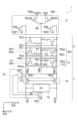
- FIG. 2 is a circuit diagram showing a detailed configuration example of the semiconductor memory device according to the first embodiment.
- the bit line BL[n] includes a first read bit line RBLL, a second read bit line RBLR, and a write bit line WBL.
- a first read bit line (first voltage supply line) RBLL supplies a predetermined voltage (first voltage) so that the fuse element F and the reference resistance element can be biased. Bias is, for example, voltage application.
- the fuse element F includes a first fuse element F1 and a second fuse element F2 shown in FIG.
- the reference resistance elements include a first reference resistance element RF1 and a second reference resistance element RF2 shown in FIG.
- the second read bit line (third voltage supply line) RBLR supplies the first voltage so that the fuse element F and the reference resistance element can be biased.
- a write bit line (second voltage supply line) WBL supplies a predetermined voltage (second voltage) different from the first voltage so that the fuse element F and the reference resistor element can be biased.
- the first voltage in the write operation is, for example, the ground voltage (0 V).
- the second voltage in the write operation is, for example, the fuse power supply voltage VDDFIL. Therefore, in a write operation, the first voltage is lower than the second voltage.
- the first voltage in the read operation is, for example, the power supply voltage (reference voltage) VDD.
- the second voltage in the read operation is, for example, the ground voltage. Therefore, in a read operation, the first voltage is higher than the second voltage.
- the second voltage (fuse power supply voltage VDDFIL) in the write operation is higher than the first voltage (power supply voltage VDD) in the read operation.
- the fuse power supply voltage VDDFIL is, for example, about 1.8V.
- the power supply voltage VDD is, for example, about 0.8V.
- the memory cell MC has a first memory cell MC1 and a second memory cell MC2.
- the first memory cell MC1 is arranged in the left column of the two columns of memory cells MC shown in FIG.
- the second memory cell MC2 is arranged in the right column of the two columns of memory cells MC shown in FIG.
- FIG. 2 exemplifies a case where four memory cells MC are arranged in two columns (2 bits) ⁇ 2 rows (2 rows). is not limited to, and may be, for example, one line. In the following, unless otherwise specified, it is assumed that a plurality of memory cells MC are arranged in a plurality of columns and a plurality of rows.
- first memory cells MC1 and the number of second memory cells MC2 are the same.
- the first memory cell MC1 and the second memory cell MC2 are arranged substantially symmetrically (for example, substantially left-right symmetrically) with the write bit line WBL interposed therebetween.
- the first read bit line RBLL and the second read bit line RBLR have substantially the same capacitance.
- the first memory cells MC1 and the second memory cells MC2 arranged in two columns are configured as one unit.
- the first memory cells MC1 and the second memory cells MC2 arranged in two columns may be arranged in plural units in the row direction.
- FIG. 2 A configuration in which a plurality of memory cells MC are arranged in the column direction is hereinafter referred to as a bit configuration.
- FIG. 2 exemplifies one bit configuration in two columns. However, other bit configurations do not necessarily have to be the same configurations. In addition, below, one bit configuration will be described assuming that a plurality of bit configurations have the same configuration.
- the first memory cell MC1 has a first fuse element F1 and a first access transistor TRA1.
- a first fuse element (first memory element) F1 is connected between a first read bit line RBLL (first access transistor TRA1) and a write bit line WBL.
- the first fuse element F1 has a resistance value according to the first state or the second state.
- a first access transistor (first cell transistor) TRA1 is connected between the first fuse element F1 and the first read bit line RBLL. Therefore, the first fuse element F1 is not directly connected to the first read bit line RBLL, but is connected to the first read bit line RBLL via the first access transistor TRA1. This allows the read operation to be performed more appropriately, as will be described later.
- the gates of the first access transistor TRA1 are connected to word lines WL1, WL3, .
- the first fuse element F1 is biased by the fuse power supply voltage VDDFIL or the power supply voltage VDD.
- the first access transistor TRA1 is, for example, an NMOS (n-channel Metal Oxide Semiconductor) transistor.
- the first fuse element F1 and the first access transistor TRA1 are connected in series.
- the second memory cell MC2 has a second fuse element F2 and a second access transistor TRA2.
- the second fuse element (second memory element) F2 is connected between the write bit line WBL and the second read bit line RBLR (second access transistor TRA2).
- the second fuse element F2 has a resistance value according to the first state or the second state.
- a second access transistor (second cell transistor) TRA2 is connected between the second fuse element F2 and the second read bit line RBLR. Therefore, the second fuse element F2 is connected to the second read bit line RBLR through the second access transistor TRA2 without being directly connected to the second read bit line RBLR. This allows the read operation to be performed more appropriately, as will be described later.
- the gates of the second access transistors TRA2 are connected to the word lines WL0, WL2, .
- the second fuse element F2 is biased by the fuse power supply voltage VDDFIL or the power supply voltage VDD.
- the second access transistor TRA2 is, for example, an NMOS transistor.
- the second fuse element F2 and the second access transistor TRA2 are connected in series.
- the semiconductor memory device of this embodiment has a plurality of word lines WL0, WL1, WL2, . . . extending in the row direction.
- Each word line WL0, WL1, WL2, . . . turns on or off the first access transistor TRA1 and the second access transistor TRA2 in each memory cell MC.
- word lines WL0 and WL2 turn on or off the second access transistor TRA2 of the right second memory cell MC2.
- the word lines WL1 and WL3 turn on or off the first access transistor TRA1 of the left first memory cell MC1.
- the readout circuit 7 has a reference voltage generator 71 , a comparator 72 , a comparison controller 73 , and a bit line separator 74 .
- the comparison unit 72 may also be called a sense amplifier (SA).
- the reference voltage generator 71 generates a reference voltage that is compared with the voltage generated by biasing the fuse element F in the read operation.
- the reference voltage is a voltage generated by biasing the first fuse element F1 and the second fuse element F2, which have resistance values corresponding to the first state, based on the first voltage and the second voltage, and a reference voltage corresponding to the second state. and a voltage that the first fuse element F1 and the second fuse element F2 having the same resistance are biased based on the first voltage and the second voltage.
- the reference voltage generator 71 has a first reference voltage generator 711 and a second reference voltage generator 712 .
- the first reference voltage generator 711 is connected between the first read bit line RBLL and the write bit line WBL.
- the first reference voltage generator 711 generates a reference voltage when the second memory cell MC2 is read.
- the second reference voltage generator 712 is connected between the write bit line WBL and the second read bit line RBLR.
- the second reference voltage generator 712 generates a reference voltage when the read operation of the first memory cell MC1 is performed.
- the first reference voltage generator 711 and the second reference voltage generator 712 are arranged substantially symmetrically (for example, substantially left-right symmetrically) with the write bit line WBL interposed therebetween.
- the first reference voltage generator 711 has a first reference resistance element RF1 and a first reference transistor TRF1.
- the first reference resistance element RF1 is connected between the first read bit line RBLL (first reference transistor TRF1) and the write bit line WBL.
- the first reference transistor TRF1 is connected between the first reference resistance element RF1 and the first read bit line RBLL. Therefore, the first reference resistive element RF1 is not directly connected to the first read bit line RBLL, but is connected to the first read bit line RBLL via the first reference transistor TRF1.
- the gate of the first reference transistor TRF1 is connected to the word line RWL1.
- the first reference resistor element RF1 is biased by the power supply voltage VDD.
- the first reference transistor TRF1 is, for example, an NMOS transistor.
- the first reference resistive element RF1 and the first reference transistor TRF1 are connected in series.
- the second reference voltage generator 712 has a second reference resistor element RF2 and a second reference transistor TRF2.
- the second reference resistance element RF2 is connected between the write bit line WBL and the second read bit line RBLR (second reference transistor TRF2).
- the second reference transistor TRF2 is connected between the second reference resistance element RF2 and the second read bit line RBLR. Therefore, the second reference resistance element RF2 is not directly connected to the second read bit line RBLR, but is connected to the second read bit line RBLR via the second reference transistor TRF2.
- the gate of the second reference transistor TRF2 is connected to the word line RWL0.
- the second reference resistance element RF2 is biased by the power supply voltage VDD.
- the second reference transistor TRF2 is, for example, an NMOS transistor.
- the second reference resistive element RF2 and the second reference transistor TRF2 are connected in series.
- the first reference resistor element RF1, the second reference resistor element RF2, the first reference transistor TRF1, and the second reference transistor TRF2 are arranged substantially symmetrically across the write bit line WBL.
- first reference resistance element RF1 and the second reference resistance element RF2 have substantially the same resistance value, for example.
- the comparator 72 compares the reference voltage with the voltage generated by biasing the first fuse element F1 or the second fuse element F2 with the first voltage and the second voltage. More specifically, the comparator 72 compares the voltage of the first read bit line RBLL and the voltage of the second read bit line RBLR. That is, when reading the first memory cell MC1, the decoder 4 selects the first memory cell MC1 and the second reference voltage generator 712, and the comparator 72 compares the voltages of the two bit lines. When reading the second memory cell MC2, the decoder 4 selects the second memory cell MC2 and the first reference voltage generator 711, and the comparator 72 compares the voltages of the two bit lines. Thereby, the resistance value of the fuse element F of the memory cell MC to be read, that is, the unwritten state (“0”) or the written state (“1”) is read. More specifically, the comparator 72 amplifies and compares the potential difference between the two bit lines.
- the comparison control section 73 causes the comparison section 72 to start comparison at timing according to the voltages of the first read bit line RBLL and the second read bit line RBLR.
- the comparison control section 73 has a NAND circuit ND1 and a comparison control transistor TRC.
- Two inputs of the NAND circuit ND1 are electrically connected to the first read bit line RBLL and the second read bit line RBLR.
- the output of the NAND circuit ND1 is electrically connected to the gate of the comparison control transistor TRC.
- the NAND circuit ND1 outputs a high signal when the voltage of at least one of the first read bit line RBLL and the second read bit line RBLR is lower than the first predetermined value.
- the comparison control transistor TRC is connected between the comparison section 72 and the ground.
- the gate of the comparison control transistor TRC is connected to the output of the NAND circuit ND1 and receives the signal SE. Outputting a high signal SE from the NAND circuit ND1 turns on the comparison control transistor TRC.
- the comparison control transistor TRC causes the comparison unit 72 to start comparison by turning it on.
- the bit line isolation section 74 electrically isolates the bit lines. As a result, when the comparison unit 72 amplifies the potential difference, it is possible to suppress the influence of the capacitance of the bit line. As a result, power consumption can be suppressed.
- the bit line isolation section 74 has a first isolation transistor TRS1 and a second isolation transistor TRS2.
- the first isolation transistor TRS1 is connected between the first read bit line RBLL and the first isolation read bit line LBLL.
- a signal CS is input to the gate of the first separation transistor TRS1.
- the first isolation transistor TRS1 electrically connects the first read bit line RBLL and the first isolation read bit line LBLL when turned on, and electrically connects the first read bit line RBLL and the first isolation read when turned off.
- the bit line LBLL is electrically disconnected.
- the first isolation transistor TRS1 is, for example, an NMOS transistor.
- the signal CS has a signal level corresponding to the signal level of the signal SE output from the NAND circuit ND1 through wiring (not shown), for example.
- the second isolation transistor TRS2 is connected between the second read bit line RBLR and the second isolation read bit line LBLR.
- a signal CS is input to the gate of the second separation transistor TRS2.
- the second isolation transistor TRS2 electrically connects the second read bit line RBLR and the second isolation read bit line LBLR when turned on, and electrically connects the second read bit line RBLR and the second isolation read line when turned off.
- the bit line LBLR is electrically disconnected.
- the second isolation transistor TRS2 is, for example, an NMOS transistor.
- the semiconductor memory device 1 further includes a voltage supply section 8 .
- the voltage supply unit 8 is omitted in FIG.
- Voltage supply unit 8 is connected between fuse power supply 6 and memory cell array 2 .
- the voltage supply unit 8 controls voltage supply by the write bit line WBL, the first read bit line RBLL, and the second read bit line RBLR.
- the operation of the voltage supply section 8 is controlled by the decoder 4, for example.
- the voltage supply unit 8 has a first blow transistor TRB1, a second blow transistor TRB2, a third blow transistor TRB3, a read transistor TRR, a first precharge transistor TRP1, and a second precharge transistor TRP2. .
- the first blow transistor TRB1 is connected between the node N1 and the ground.
- the node N1 is provided between the power supply voltage node VDD (first precharge transistor TRP1) and the memory cell array 2 on the first read bit line RBLL.
- a BLOW signal is input to the gate of the first blow transistor TRB1.
- the write operation of the first memory cell MC1 is performed by turning on the first blow transistor TRB1.
- the first blow transistor TRB1 is, for example, an NMOS transistor.
- the second blow transistor TRB2 is connected between the node N2 and the ground.
- the node N2 is provided between the power supply voltage node VDD (second precharge transistor TRP2) and the memory cell array 2 on the second read bit line RBLR.
- a BLOW signal is input to the gate of the second blow transistor TRB2.
- the write operation of the second memory cell MC2 is performed by turning on the second blow transistor TRB2.
- the second blow transistor TRB2 is, for example, an NMOS transistor.
- the third blow transistor TRB3 is connected between the node N3 and the fuse power supply voltage node VDDFIL. Node N3 is provided between fuse power supply voltage node VDDFIL and memory cell array 2 on write bit line WBL.
- a /BLOW signal is input to the gate of the third blow transistor TRB3.
- the write operation of the first memory cell MC1 or the second memory cell MC2 is performed by turning on the third blow transistor TRB3.
- the third blow transistor TRB3 is, for example, a PMOS (p-channel Metal Oxide Semiconductor) transistor.
- the read transistor TRR is connected between the node N3 and the ground. Node N3 is provided between fuse power supply voltage node VDDFIL (third blow transistor TRB3) and memory cell array 2 on write bit line WBL. A READ signal is input to the gate of the read transistor TRR. The read operation of the first memory cell MC1 or the second memory cell MC2 is performed by turning on the read transistor TRR.
- the read transistor TRR is, for example, an NMOS transistor.
- the first precharge transistor TRP1 is connected between the power supply voltage node VDD and the memory cell array 2 (node N1). A /PRE signal is input to the gate of the first precharge transistor TRP1. By turning on the first precharge transistor TRP1, the first read bit line RBLL is precharged in the read operation. Details of the precharge will be described later with reference to FIG.
- the first precharge transistor TRP1 is, for example, a PMOS transistor.
- the second precharge transistor TRP2 is connected between the power supply voltage node VDD and the memory cell array 2 (node N2). A /PRE signal is input to the gate of the second precharge transistor TRP2. By turning on the second precharge transistor TRP2, the second read bit line RBLR is precharged in the read operation. Details of the precharge will be described later with reference to FIG.
- the second precharge transistor TRP2 is, for example, a PMOS transistor.
- FIG. 3 is a timing chart showing an example of write operation of the semiconductor memory device according to the first embodiment.
- FIG. 3 shows a timing chart of the write operation of the second memory cell MC2.
- the BLOW signal In the initial state, the BLOW signal is in a high state. Therefore, the first blow transistor TRB1 and the second blow transistor TRB2 are on. The /BLOW signal is in a high state. Therefore, the third blow transistor TRB3 is off. The signals on word lines WL0 and RWL1 are in the low state. Therefore, the second access transistor TRA2 and the first reference transistor TRF1 are off.
- the signal on word line WL0 becomes high. This turns on the second access transistor TRA2.
- the /BLOW signal goes low. This turns on the third blow transistor TRB3. As a result, the voltage of the write bit line WBL rises, and the second fuse element F2 is biased by the fuse power supply voltage VDDFIL to enter the write state.
- the signal SE is in a low state during the write operation. Therefore, comparison control transistor TRC is in an off state. Signal CS is in the low state. Therefore, the first isolation transistor TRS1 and the second isolation transistor TRS2 are off. That is, the first read bit line RBLL and the second read bit line RBLR are electrically disconnected from the first separated read bit line LBLL and the second separated read bit line LBLR, respectively.
- the read transistor TRR, the first precharge transistor TRP1, and the second precharge transistor TRP2 are in the off state during the write operation.
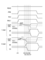
- FIG. 4 is a timing chart showing an example of read operation of the semiconductor memory device according to the first embodiment.
- FIG. 4 shows a timing chart of the read operation of the second memory cell MC2.
- the voltage supply unit 8 supplies the first voltage to the first read bit line RBLL and the second read bit line RBLR in advance, and preliminarily supplies the write bit line RBLL with the first voltage.
- the voltage supply unit 8 stops supplying the first voltage to the first read bit line RBLL and the second read bit line RBLR.
- the decoder (cell transistor control unit) 4 controls the first access transistor TRA1 of the first memory cell MC1 to be read or the first access transistor TRA1 of the second memory cell MC2 to be read. 2 Turn on the access transistor TRA2. In this manner, charge extraction is performed.
- the READ signal In the initial state, the READ signal is in a high state. Therefore, the read transistor TRR is on. As a result, the write bit line WBL is discharged to 0V, for example.
- the /PRE signal is in the low state. Therefore, the first precharge transistor TRP1 and the second precharge transistor TRP2 are on.
- the signals on word lines WL0 and RWL1 are in the low state. Therefore, the second access transistor TRA2 and the first reference transistor TRF1 are off.
- the signal SE is in a low state. Therefore, comparison control transistor TRC is in an off state. Signal CS is in a high state. Therefore, the first isolation transistor TRS1 and the second isolation transistor TRS2 are on. That is, the first read bit line RBLL and the second read bit line RBLR are electrically connected to the first separated read bit line LBLL and the second separated read bit line LBLR, respectively.
- the voltages of the first separated read bit line LBLL (first read bit line RBLL) and the second separated read bit line LBLR (second read bit line RBLR) are precharged to the power supply voltage VDD.
- All first access transistors TRA1, all second access transistors TRA2, first reference transistors TRF1 and second reference transistors TRF2 shown in FIG. 2 are in an off state. Therefore, regardless of whether the state of the memory cell MC is in the written state (“1”) or in the unwritten state (“0”), the electric charge does not escape from the first separation read bit line LBLL. and stored in the second separated read bit line LBLR.
- the /PRE signal becomes high.
- the first precharge transistor TRP1 and the second precharge transistor TRP2 are turned off.
- the signals on word lines WL0 and RWL1 go high substantially at the same time.
- the second access transistor TRA2 and the first reference transistor TRF1 are turned on substantially simultaneously.
- the voltages of the first separated read bit line LBLL and the second separated read bit line LBLR drop. This is because the charges accumulated in the first separated read bit line LBLL and the second separated read bit line LBLR flow through the write bit line WBL.
- a current flowing through the write bit line WBL flows to the ground connected to the source of the read transistor TRR.
- the voltage drop speed differs between the first separated read bit line LBLL and the second separated read bit line LBLR.
- the rate of decrease in the voltage of the first separated read bit line LBLL is determined by the resistance value of the first reference resistance element RF1. Therefore, the voltage drop speed of the first separated read bit line LBLL does not change depending on the state (0/1) of the second fuse element F2 of the second memory cell MC2.
- the voltage drop speed of the second separated read bit line LBLR changes depending on the state (0/1) of the second fuse element F2 of the second memory cell MC2.
- the voltage drop speed of the second separation read bit line LBLR is equal to that of the first separation read bit line. It is slower than the voltage drop rate of LBLL.
- the voltage of the first separated read bit line LBLL becomes lower than the logic threshold (first predetermined value) of the NAND circuit ND1.
- the NAND circuit ND1 inputs the signal SE that changes from low to high to the gate of the comparison control transistor TRC.
- the signal CS becomes low at time t17 due to the signal SE becoming high.
- the first isolation transistor TRS1 and the second isolation transistor TRS2 are turned off.
- the first read bit line RBLL and the second read bit line RBLR are electrically disconnected from the first separated read bit line LBLL and the second separated read bit line LBLR, respectively.
- the comparator 72 performs voltage comparison by turning on the comparison control transistor TRC. That is, the comparison control section 73 causes the comparison section 72 to start comparison at the timing when the voltage of at least one of the first read bit line RBLL and the second read bit line RBLR becomes lower than the first predetermined value. After time t16, the comparator 72 amplifies and compares the potential difference between the first separated read bit line LBLL and the second separated read bit line LBLR.
- the /PRE signal goes low, and the signals on word lines WL0 and RWL1 go low.
- the first precharge transistor TRP1 and the second precharge transistor TRP2 are turned on, and the second access transistor TRA2 and the first reference transistor TRF1 are turned off.
- the voltage drop speed of the second separation read bit line LBLR is equal to that of the first separation read bit line. Faster than the LBLL voltage drop rate.
- the voltage of the second separated read bit line LBLR becomes lower than the logic threshold (first predetermined value) of the NAND circuit ND1.
- the NAND circuit ND1 inputs the signal SE that changes from low to high to the gate of the comparison control transistor TRC.
- the signal CS becomes low at time t14 due to the signal SE becoming high.
- the first isolation transistor TRS1 and the second isolation transistor TRS2 are turned off.
- the first read bit line RBLL and the second read bit line RBLR are electrically disconnected from the first separated read bit line LBLL and the second separated read bit line LBLR, respectively.
- the comparator 72 compares the voltages by turning on the comparison control transistor TRC. That is, the comparison control section 73 causes the comparison section 72 to start comparison at the timing when the voltage of at least one of the first read bit line RBLL and the second read bit line RBLR becomes lower than the first predetermined value. After time t13, the comparator 72 amplifies and compares the potential difference between the first separated read bit line LBLL and the second separated read bit line LBLR.
- the /PRE signal goes low, and the signals on word lines WL0 and RWL1 go low.
- the first precharge transistor TRP1 and the second precharge transistor TRP2 are turned on, and the second access transistor TRA2 and the first reference transistor TRF1 are turned off.
- the comparison start timing by the comparator 72 differs depending on the state (0/1) of the second memory cell MC2. That is, the timing from the rise of the voltage of the word line to the activation of the sense amplifier is set so that the logic threshold value (first predetermined value) of the NAND circuit ND1 of the first separated read bit line LBLL and the second separated read bit line LBLR precedes. is determined in a self-consistent manner at a rate lower than .
- the BLOW signal and the /BLOW signal are not shown in FIG. 4, the first blow transistor TRB1, the second blow transistor TRB2 and the third blow transistor TRB3 are in the off state.
- the first memory cell MC1 is connected between the first read bit line RBLL and the write bit line WBL.
- the first access transistor TRA1 is connected between the first fuse element F1 and the first read bit line RBLL.
- the second memory cell MC2 is connected between the write bit line WBL and the second read bit line RBLR.
- the second access transistor TRA2 is connected between the second fuse element F2 and the second read bit line RBLR.
- connection relationship (placement) between the first reference transistor TRF1 and the second reference transistor TRF2 corresponds to the connection relationship between the first access transistor TRA1 and the second access transistor TRA2.
- the first reference transistor may be connected between the first reference resistance element RF1 and the write bit line WBL.
- the second reference resistance element RF2 may be connected between the second reference resistance element RF2 and the write bit line WBL.
- FIG. 5 is a circuit diagram illustrating bit line capacitance in a semiconductor memory device 1a according to a comparative example.
- FIG. 6 is a circuit diagram illustrating bit line capacitance in the semiconductor memory device 1 according to the first embodiment.
- the comparative example differs from the first embodiment in the arrangement of fuse elements and access transistors in memory cells MC. Note that in FIG. 5, a first bit line BLL and a second bit line BLR are provided instead of the first read bit line RBLL and the second read bit line RBLR. Similarly, instead of write bit line WBL, ground line GND is provided.
- the first access transistor TRA1 of the first memory cell MC1 is connected between the first fuse element F1 and the ground line GND. Therefore, the first fuse element F1 is directly connected to the first bit line BLL.
- the second access transistor TRA2 of the second memory cell MC2 is connected between the second fuse element F2 and the ground line GND. Therefore, the second fuse element F2 is directly connected to the second bit line BLR.
- the total capacitance of the first bit lines BLL shown in FIG. 5 is expressed by Equation 1 using the bit line wiring capacitance of the first bit lines BLL.
- Total capacitance Bit line wiring capacitance (Formula 1)
- the total capacitance of the second bit line BLR shown in FIG. 5 is calculated using the bit line wiring capacitance of the second bit line BLR, the fuse element capacitance of the second fuse element F2, and the transistor diffusion capacitance of the second access transistor TRA2. It is represented by Formula 2.
- Total capacity bit line wiring capacity + (fuse element capacity + transistor diffusion capacity) x number of bits (formula 2)
- the total capacitance of the second bit lines BLR is greater than the total capacitance of the first bit lines BLL.
- the time to pull out the precharged charge in the bit lines also depends on the write data pattern. It may change significantly. In this case, in the comparative example, it may be difficult to stably perform the read operation using the precharge shown in FIG.
- the total capacitance of each of the first read bit line RBLL and the second read bit line RBLR is substantially constant regardless of the write data pattern. Therefore, the time for extracting the charges precharged in the bit line (the rate at which the voltage of the bit line drops) is also substantially constant regardless of the write data pattern. As a result, the read operation using precharge can be performed more stably.
- FIG. 7 is a diagram showing temporal changes in the voltage of the bit line.
- the upper part of FIG. 7 is a graph showing the time change of the voltage of the word line.
- the middle part of FIG. 7 is a graph showing the time change of the bit line voltage in the comparative example.
- the lower part of FIG. 7 is a graph showing the time change of the bit line voltage in the first embodiment.
- the vertical axis of the graph shown in FIG. 7 is voltage.
- the horizontal axis of the graph shown in FIG. 7 is time. Note that the time shown on the horizontal axis is common to all graphs.
- the word line voltage includes, for example, word lines RWL0, RWL1, WL0, and WL1.
- Bit line voltages Vb0 and Vb1 of bit lines electrically connected to memory cells MC are indicated by solid lines.
- a bit line voltage Vb0 indicates a voltage when the memory cell MC is in an unwritten state.
- a bit line voltage Vb1 indicates a voltage when the memory cell MC is in the write state.
- the reference voltage Vref of the reference bit line electrically connected to the reference voltage generator 71 is indicated by a dashed line.
- bit line and reference bit line in the comparative example correspond to the second bit line BLR and first bit line BLL shown in FIG. 5, respectively.
- a bit line and a reference bit line in the first embodiment correspond to the second read bit line RBLR and the first read bit line RBLL shown in FIG. 6, respectively.
- the word line voltage is low in the initial state.
- the word line voltage becomes High at time ta. This activates the word line.
- the second fuse element F2 is biased by the power supply voltage VDD and DC current continues to flow through the second fuse element F2.
- bit line voltages Vb0 and Vb1 and the reference voltage Vref are zero, for example.
- bit line voltages Vb0 and Vb1 and the reference voltage Vref rise. Since the fuse element is blown, the bit line voltage Vb1 is higher than the bit line voltage Vb0, and it takes time to stabilize the voltage.
- bit line voltage Vb1 exceeds the reference voltage Vref. That is, after time tc, reference voltage Vref attains a voltage level between bit line voltage Vb0 and bit line voltage Vb1. Therefore, in the comparative example, it is necessary for the comparison unit 72 to perform the comparison after sufficiently waiting until at least the time tc has passed.
- temporal changes of the bit line voltages Vb0 and Vb1 and the reference voltage Vref in the comparative example are examples.
- bit line voltages Vb0 and Vb1 and the reference voltage Vref are precharged to the power supply voltage VDD.
- the word line voltage becomes high. Also, at time ta, the bit line voltages Vb0 and Vb1 and the reference voltage Vref decrease. This is because the first access transistor TRA1 and the second access transistor TRA2 are turned on, and charges are extracted from the first read bit line RBLL and the second read bit line RBLR.
- the rate of decrease of reference voltage Vref after time ta is between the rate of decrease of bit line voltage Vb0 and the rate of decrease of bit line voltage Vb1.
- the access transistor is arranged between the fuse element and the read bit line. As a result, it is possible to suppress variations in the change speed (decrease speed) of the voltage of the bit line when the charge is extracted, depending on the pattern of the write data. As a result, the read operation can be stably performed. Also, as shown in FIG.
- the potential difference between the bit line voltages Vb0 and Vb1 and the reference voltage Vref widens faster than in the comparative example.
- the time from word line activation to sense amplifier activation can be shortened.
- high-speed read operation becomes possible.
- the potential difference between the bit line voltages Vb0 and Vb1 and the reference voltage Vref is generated in a relatively short time after the word line is activated due to the difference in the speed of extracting electric charges. is occurring. Since the speed at which electric charges are extracted is caused by the difference in resistance values, there is a possibility that a sufficient potential difference can be obtained regardless of the magnitude of the precharge voltage at the start of reading. For example, the power supply voltage VDD can be lowered within a range in which the comparing section 72 can appropriately perform comparison. Thereby, the voltage can be lowered.
- the potential difference between the first voltage and the second voltage is between the first read bit line RBLL and the second read bit line RBLR after the decoder 4 turns on the first access transistor TRA1 or the second access transistor TRA2. is the potential difference corresponding to the difference in the voltage change rate of
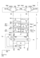
- FIG. 8 is a circuit diagram showing a detailed configuration example of the semiconductor memory device 1 according to the second embodiment.
- the second embodiment differs from the first embodiment in that the write bit line WBL is grounded.
- the write bit line WBL in the second embodiment corresponds to the ground line GND in the comparative example.
- the first voltage in the write operation is, for example, the fuse power supply voltage VDDFIL.
- the second voltage in the write operation is, for example, the ground voltage (0V). Therefore, in a write operation, the first voltage is higher than the second voltage.
- the first voltage in the read operation is, for example, power supply voltage VDD.
- the second voltage in the read operation is, for example, the ground voltage. Therefore, in a read operation, the first voltage is higher than the second voltage.
- the first voltage (fuse power supply voltage VDDFIL) in the write operation is higher than the first voltage (power supply voltage VDD) in the read operation.
- the voltage supply section 8 in the second embodiment does not have the third blow transistor TRB3 and the read transistor TRR, unlike the first embodiment.
- the first blow transistor TRB1 is connected between the node N4 on the first read bit line RBLL and the fuse power supply voltage node VDDFIL.
- a /BLOWL signal is input to the gate of the first blow transistor TRB1.
- the first blow transistor TRB1 is, for example, a PMOS transistor.
- the second blow transistor TRB2 is connected between the node N5 on the second read bit line RBLR and the fuse power supply voltage node VDDFIL.
- a /BLOWR signal is input to the gate of the second blow transistor TRB2.
- the second blow transistor TRB2 is, for example, a PMOS transistor.
- the first precharge transistor TRP1 is connected between the node N4 on the first read bit line RBLL and the power supply voltage node VDD.
- the second precharge transistor TRP2 is connected between the node N5 on the second read bit line RBLR and the power supply voltage node VDD.
- the write bit line WBL is connected to the ground and fixed at the ground voltage. That is, the voltage supply unit 8 fixes the write bit line WBL to the second voltage (ground voltage).
- FIG. 9 is a timing chart showing an example of write operation of the semiconductor memory device 1 according to the second embodiment.
- the /BLOWL signal and /BLOWR signal are in a high state. Therefore, the first blow transistor TRB1 and the second blow transistor TRB2 are off.
- the signals on word lines WL0 and RWL1 are in the low state. Therefore, the second access transistor TRA2 and the first reference transistor TRF1 are off.
- the signal on word line WL0 becomes high. This turns on the second access transistor TRA2.
- the /BLOWR signal goes low. This turns on the second blow transistor TRB2. As a result, the voltage of the second read bit line RBLR rises, and the second fuse element F2 is biased by the fuse power supply voltage VDDFIL to enter the write state.
- the /BLOWR signal goes high and the signal on word line WL0 goes low.
- the second blow transistor TRB2 is turned off, and the second access transistor TRA2 is turned off.
- FIG. 10 is a timing chart showing an example of read operation of the semiconductor memory device 1 according to the second embodiment.
- the READ signal is not input.
- Other read operations of the semiconductor memory device 1 according to the second embodiment are the same as in FIG. 4 described in the first embodiment.
- the write bit line WBL may be grounded as in the second embodiment. Also in this case, the same effect as in the first embodiment can be obtained.
- FIG. 11 is a circuit diagram showing a detailed configuration example of the semiconductor memory device 1 according to the third embodiment.
- the third embodiment differs from the first embodiment in that the precharge level of the first read bit line RBLL and the second read bit line RBLR is 0V.
- the first voltage in the write operation is, for example, the ground voltage (0 V).
- the second voltage in the write operation is, for example, the fuse power supply voltage VDDFIL. Therefore, in a write operation, the first voltage is lower than the second voltage.
- the first voltage in the read operation is, for example, the ground voltage.
- the second voltage in the read operation is, for example, power supply voltage VDD. Therefore, in a read operation, the first voltage is lower than the second voltage.
- the second voltage (fuse power supply voltage VDDFIL) in the write operation is higher than the second voltage (power supply voltage VDD) in the read operation.
- the voltage supply section 8 in the third embodiment does not have the first blow transistor TRB1 and the second blow transistor TRB2.
- the third blow transistor TRB3 is connected between the node N6 on the write bit line WBL and the fuse power supply voltage node VDDFIL.
- the read transistor TRR is connected between the node N6 on the write bit line WBL and the power supply voltage node VDD.
- a /READ signal is input to the gate of the read transistor TRR.
- the read transistor TRR is, for example, a PMOS transistor.
- the first precharge transistor TRP1 is connected between one end of the first read bit line RBLL and the ground.
- a PRE signal is input to the gate of the first precharge transistor TRP1.
- the first precharge transistor TRP1 is, for example, an NMOS transistor.
- the second precharge transistor TRP2 is connected between one end of the second read bit line RBLR and the ground.
- a PRE signal is input to the gate of the second precharge transistor TRP2.
- the second precharge transistor TRP2 is, for example, an NMOS transistor.
- the comparison control unit 73 has an OR circuit OR1 instead of the NAND circuit ND1 in the first embodiment.
- Two inputs of the OR circuit OR1 are electrically connected to the first read bit line RBLL and the second read bit line RBLR.
- the output of the OR circuit OR1 is electrically connected to the gate of the comparison control transistor TRC.
- the OR circuit OR1 outputs a high signal when the voltage of at least one of the first read bit line RBLL and the second read bit line RBLR is higher than the second predetermined value.
- FIG. 12 is a timing chart showing a write operation example of the semiconductor memory device 1 according to the third embodiment.
- the PRE signal In the initial state, the PRE signal is in a high state. Therefore, the first precharge transistor TRP1 and the second precharge transistor TRP2 are on.
- the first precharge transistor TRP1 and the second precharge transistor TRP2 operate in substantially the same manner as the first blow transistor TRB1 and the second blow transistor TRB2 in the first embodiment.
- Other operations of the semiconductor memory device 1 according to the third embodiment are the same as in FIG. 3 described in the first embodiment.
- FIG. 13 is a timing chart showing an example of read operation of the semiconductor memory device 1 according to the third embodiment.
- the /READ signal In the initial state, the /READ signal is in a low state. Therefore, the read transistor TRR is on. As a result, the write bit line WBL is precharged to the power supply voltage VDD. All the first access transistors TRA1, all the second access transistors TRA2, the first reference transistors TRF1 and the second reference transistors TRF2 shown in FIG. 11 are in the off state. Therefore, regardless of whether the memory cell MC is in the written state (“1”) or in the unwritten state (“0”), the charge is accumulated in the write bit line WBL without being discharged. be.
- the PRE signal In the initial state, the PRE signal is in a high state. Therefore, the first precharge transistor TRP1 and the second precharge transistor TRP2 are on. As a result, the voltages of the first read bit line RBLL (first separated read bit line LBLL) and the second read bit line RBLR (second separated read bit line LBLR) are discharged to 0V, for example.
- the PRE signal becomes low.
- the first precharge transistor TRP1 and the second precharge transistor TRP2 are turned off.
- the signals on word lines WL0 and RWL1 go high substantially at the same time.
- the second access transistor TRA2 and the first reference transistor TRF1 are turned on substantially simultaneously.
- the voltages of the first separated read bit line LBLL and the second separated read bit line LBLR rise. This is because the first separated read bit line LBLL and the second separated read bit line LBLR discharged to 0V are charged to the level of the power supply voltage VDD through the read transistor TRR and the write bit line WBL.
- the voltage rise speed differs between the first separated read bit line LBLL and the second separated read bit line LBLR.
- the rate of increase in the voltage of the first separated read bit line LBLL is determined by the resistance value of the first reference resistance element RF1. Therefore, the voltage rising speed of the first separated read bit line LBLL does not change depending on the state (0/1) of the second fuse element F2 of the second memory cell MC2.
- the rate of increase of the voltage of the second separated read bit line LBLR changes depending on the state (0/1) of the second fuse element F2 included in the second memory cell MC2.
- the rate of increase of the voltage of the second separated read bit line LBLR is equal to that of the first separated read bit line. Slower than the LBLL voltage rise rate.
- the voltage of the first separated read bit line LBLL becomes higher than the logic threshold (second predetermined value) of the OR circuit OR1.
- the OR circuit OR1 inputs the signal SE that changes from low to high to the gate of the comparison control transistor TRC.
- the signal CS becomes low at time t54 due to the signal SE becoming high.
- the first isolation transistor TRS1 and the second isolation transistor TRS2 are turned off.
- the first read bit line RBLL and the second read bit line RBLR are electrically disconnected from the first separated read bit line LBLL and the second separated read bit line LBLR, respectively.
- the comparator 72 compares the voltages by turning on the comparison control transistor TRC. That is, the comparison control section 73 causes the comparison section 72 to start comparison at the timing when the voltage of at least one of the first read bit line RBLL and the second read bit line RBLR becomes higher than the second predetermined value. After time t53, the comparator 72 amplifies and compares the potential difference between the first separated read bit line LBLL and the second separated read bit line LBLR.
- the PRE signal goes high, and the signals on word lines WL0 and RWL1 go low.
- the first precharge transistor TRP1 and the second precharge transistor TRP2 are turned on, and the second access transistor TRA2 and the first reference transistor TRF1 are turned off.
- the rate of increase of the voltage of the second separated read bit line LBLR is equal to that of the first separated read bit line. It is faster than the rising speed of the voltage of LBLL.
- the voltage of the second separated read bit line LBLR becomes higher than the logic threshold (second predetermined value) of the OR circuit OR1.
- the OR circuit OR1 inputs the signal SE that changes from low to high to the gate of the comparison control transistor TRC.
- the signal CS becomes low at time t57 due to the signal SE becoming high.
- the first isolation transistor TRS1 and the second isolation transistor TRS2 are turned off.
- the first read bit line RBLL and the second read bit line RBLR are electrically disconnected from the first separated read bit line LBLL and the second separated read bit line LBLR, respectively.
- the comparator 72 compares the voltages by turning on the comparison control transistor TRC. That is, the comparison control section 73 causes the comparison section 72 to start comparison at the timing when the voltage of at least one of the first read bit line RBLL and the second read bit line RBLR becomes higher than the second predetermined value. After time t56, the comparator 72 amplifies and compares the potential difference between the first separated read bit line LBLL and the second separated read bit line LBLR.
- the PRE signal goes high, and the signals on word lines WL0 and RWL1 go low.
- the first precharge transistor TRP1 and the second precharge transistor TRP2 are turned on, and the second access transistor TRA2 and the first reference transistor TRF1 are turned off.
- the comparison start timing by the comparator 72 differs depending on the state (0/1) of the second memory cell MC2. That is, the timing from the rise of the voltage of the word line to the activation of the sense amplifier is determined by the logic threshold value (second predetermined value) of the OR circuit OR1 of the first separated read bit line LBLL and the second separated read bit line LBLR. can be determined self-consistently at a speed higher than .
- the precharge level of the first read bit line RBLL and the second read bit line RBLR may be 0V as in the third embodiment. Also in this case, the same effect as in the first embodiment can be obtained.
- FIG. 14 is a circuit diagram showing a detailed configuration example of the semiconductor memory device 1 according to the fourth embodiment.
- the fourth embodiment differs from the second embodiment in that the transistors included in the memory cells MC and the reference voltage generator 71 are PMOS transistors.
- the first access transistor TRA1, the second access transistor TRA2, the first reference transistor TRF1, and the second reference transistor TRF2 are, for example, PMOS transistors.
- FIG. 15 is a timing chart showing a write operation example of the semiconductor memory device 1 according to the second embodiment.
- the relationship between the high and low signals of the word lines WL0 and RWL1 is reversed compared to the second embodiment.
- Other write operations of the semiconductor memory device 1 according to the fourth embodiment are the same as those in FIG. 9 described in the second embodiment.
- FIG. 16 is a timing chart showing an example of read operation of the semiconductor memory device 1 according to the fourth embodiment.
- the relationship between the high and low signals of the word lines WL0 and RWL1 is reversed compared to the second embodiment.
- Other read operations of the semiconductor memory device 1 according to the fourth embodiment are the same as in FIG. 10 described in the second embodiment.
- the transistors included in the memory cell MC and the reference voltage generator 71 may be PMOS transistors as in the fourth embodiment. Also in this case, the same effects as in the second embodiment can be obtained. Also in the first embodiment or the third embodiment, the transistors included in the memory cells MC and the reference voltage generator 71 may be PMOS transistors.
- this technique can take the following structures. (1) one or more first memory cells connected in parallel between a first voltage supply line supplying a first voltage and a second voltage supply line supplying a second voltage different from the first voltage; , one or more second memory cells connected in parallel between the second voltage supply line and a third voltage supply line supplying the first voltage; with each of the first memory cells, a first storage element having a resistance value corresponding to the first state or the second state; a first cell transistor connected between the first memory element and the first voltage supply line; each of the second memory cells, a second storage element having a resistance value corresponding to the first state or the second state; a second cell transistor connected between the second memory element and the third voltage supply line.
- the semiconductor memory device according to any one of (1) to (3), further comprising: (5) The potential difference between the first voltage and the second voltage is the first voltage supply line and the third voltage supply line after the cell transistor control unit turns on the first cell transistor or the second cell transistor.
- the semiconductor memory device which is a potential difference corresponding to a difference in voltage change rate between and.
- (6) The semiconductor memory device according to (4) or (5), wherein the second voltage supply line is fixed to the second voltage.
- the first storage element and the second storage element having a resistance value generate a reference voltage having a voltage level between a voltage generated by being biased based on the first voltage and the second voltage.
- the semiconductor memory device according to any one of (1) to (6), further comprising: (8) The reference voltage generation unit a first reference voltage generator connected between the first voltage supply line and the second voltage supply line and configured to generate the reference voltage when a read operation of the second memory cell is performed; a second reference voltage generator connected between the second voltage supply line and the third voltage supply line for generating the reference voltage when a read operation of the first memory cell is performed; The semiconductor memory device according to (7), having (9) The semiconductor memory device according to (8), wherein the first reference voltage generator and the second reference voltage generator are arranged substantially symmetrically with the second voltage supply line interposed therebetween.
- the first reference voltage generation unit a first reference resistance element; a first reference transistor connected between the first reference resistance element and the first voltage supply line; has The second reference voltage generation unit a second reference resistance element; a second reference transistor connected between the second reference resistance element and the third voltage supply line;
- the semiconductor memory device having (11)
- the comparison unit compares the voltage of the first voltage supply line and the voltage of the third voltage supply line to determine whether the reference voltage and the first memory element or the second memory element are the same as the first memory element.
- the comparison control unit is When the first voltage is higher than the second voltage, the comparing unit performs comparison at timing when the voltage of at least one of the first voltage supply line and the third voltage supply line becomes lower than a first predetermined value. let it start When the first voltage is lower than the second voltage, the comparing unit performs the comparison at the timing when the voltage of at least one of the first voltage supply line and the third voltage supply line becomes higher than a second predetermined value.
- (13) The semiconductor memory device according to any one of (1) to (12), wherein in a read operation, the first voltage is higher than the second voltage.
- (14) In a write operation, the first voltage is lower than the second voltage, The semiconductor memory device according to (13), wherein the second voltage in write operation is higher than the first voltage in read operation.
- (16) The semiconductor memory device according to any one of (1) to (12), wherein in a read operation, the first voltage is lower than the second voltage.
- (17) In a write operation, the first voltage is lower than the second voltage, The semiconductor memory device according to (16), wherein the second voltage in write operation is higher than the second voltage in read operation.
Landscapes
- Engineering & Computer Science (AREA)
- Computer Hardware Design (AREA)
- Read Only Memory (AREA)
Priority Applications (2)
| Application Number | Priority Date | Filing Date | Title |
|---|---|---|---|
| JP2023557891A JPWO2023079863A1 (https=) | 2021-11-02 | 2022-09-27 | |
| US18/704,854 US20250006260A1 (en) | 2021-11-02 | 2022-09-27 | Semiconductor storage device |
Applications Claiming Priority (2)
| Application Number | Priority Date | Filing Date | Title |
|---|---|---|---|
| JP2021-179703 | 2021-11-02 | ||
| JP2021179703 | 2021-11-02 |
Publications (1)
| Publication Number | Publication Date |
|---|---|
| WO2023079863A1 true WO2023079863A1 (ja) | 2023-05-11 |
Family
ID=86241312
Family Applications (1)
| Application Number | Title | Priority Date | Filing Date |
|---|---|---|---|
| PCT/JP2022/036022 Ceased WO2023079863A1 (ja) | 2021-11-02 | 2022-09-27 | 半導体記憶装置 |
Country Status (3)
| Country | Link |
|---|---|
| US (1) | US20250006260A1 (https=) |
| JP (1) | JPWO2023079863A1 (https=) |
| WO (1) | WO2023079863A1 (https=) |
Citations (2)
| Publication number | Priority date | Publication date | Assignee | Title |
|---|---|---|---|---|
| JP2013251035A (ja) * | 2012-06-04 | 2013-12-12 | Toshiba Corp | 磁気ランダムアクセスメモリ |
| JP2017142869A (ja) * | 2016-02-08 | 2017-08-17 | 株式会社東芝 | 半導体記憶装置 |
-
2022
- 2022-09-27 JP JP2023557891A patent/JPWO2023079863A1/ja active Pending
- 2022-09-27 US US18/704,854 patent/US20250006260A1/en active Pending
- 2022-09-27 WO PCT/JP2022/036022 patent/WO2023079863A1/ja not_active Ceased
Patent Citations (2)
| Publication number | Priority date | Publication date | Assignee | Title |
|---|---|---|---|---|
| JP2013251035A (ja) * | 2012-06-04 | 2013-12-12 | Toshiba Corp | 磁気ランダムアクセスメモリ |
| JP2017142869A (ja) * | 2016-02-08 | 2017-08-17 | 株式会社東芝 | 半導体記憶装置 |
Also Published As
| Publication number | Publication date |
|---|---|
| US20250006260A1 (en) | 2025-01-02 |
| JPWO2023079863A1 (https=) | 2023-05-11 |
Similar Documents
| Publication | Publication Date | Title |
|---|---|---|
| US5450361A (en) | Semiconductor memory device having redundant memory cells | |
| TWI601144B (zh) | 記憶體裝置及操作記憶體裝置的方法 | |
| US7301838B2 (en) | Sense amplifier circuitry and architecture to write data into and/or read from memory cells | |
| KR101088954B1 (ko) | 프로그램이 가능한 비휘발성 메모리 | |
| US6788601B2 (en) | Semiconductor memory device and current mirror circuit | |
| US9484091B2 (en) | Resistance change memory | |
| US7599221B2 (en) | Floating gate memory device with improved reference current generation | |
| CN100570742C (zh) | 用于待机操作的低功率管理器 | |
| US20090039462A1 (en) | Efuse devices and efuse arrays thereof and efuse blowing methods | |
| JP4901211B2 (ja) | センスアンプ及び半導体記憶装置 | |
| KR20120037371A (ko) | 반도체 디바이스 | |
| KR101095730B1 (ko) | 앤티퓨즈를 기반으로 하는 반도체 메모리 장치 | |
| JP2022511134A (ja) | フラッシュメモリセルにアクセスするためのアレイの列及び行を構成する方法及び装置 | |
| JP4532951B2 (ja) | 半導体集積回路の使用方法および半導体集積回路 | |
| TWI584301B (zh) | 記憶體電路及其操作方法 | |
| JP2009064512A (ja) | 半導体記憶装置 | |
| JPH103789A (ja) | トランジスタのしきい値補正回路及び半導体記憶装置並びにしきい値補正方法 | |
| JP4615371B2 (ja) | 強誘電体メモリ | |
| US9543037B2 (en) | Semiconductor device having electrical fuse and control method thereof | |
| US20020136070A1 (en) | Semiconductor memory device adopting redundancy system | |
| US5604704A (en) | Compound semiconductor static random access memory device equipped with precharging circuit controlled by boosted signal | |
| WO2023079863A1 (ja) | 半導体記憶装置 | |
| JP2856848B2 (ja) | 半導体メモリ装置 | |
| JP2007073121A (ja) | 半導体メモリ回路 | |
| WO1992016946A1 (en) | Semiconductor memory having nonvolatile semiconductor memory cell |
Legal Events
| Date | Code | Title | Description |
|---|---|---|---|
| 121 | Ep: the epo has been informed by wipo that ep was designated in this application |
Ref document number: 22889687 Country of ref document: EP Kind code of ref document: A1 |
|
| WWE | Wipo information: entry into national phase |
Ref document number: 2023557891 Country of ref document: JP |
|
| WWE | Wipo information: entry into national phase |
Ref document number: 18704854 Country of ref document: US |
|
| NENP | Non-entry into the national phase |
Ref country code: DE |
|
| 122 | Ep: pct application non-entry in european phase |
Ref document number: 22889687 Country of ref document: EP Kind code of ref document: A1 |