WO2023079863A1 - Semiconductor memory device - Google Patents
Semiconductor memory device Download PDFInfo
- Publication number
- WO2023079863A1 WO2023079863A1 PCT/JP2022/036022 JP2022036022W WO2023079863A1 WO 2023079863 A1 WO2023079863 A1 WO 2023079863A1 JP 2022036022 W JP2022036022 W JP 2022036022W WO 2023079863 A1 WO2023079863 A1 WO 2023079863A1
- Authority
- WO
- WIPO (PCT)
- Prior art keywords
- voltage
- bit line
- supply line
- transistor
- read
- Prior art date
Links
- 239000004065 semiconductor Substances 0.000 title claims abstract description 93
- 101100478296 Arabidopsis thaliana SR45A gene Proteins 0.000 description 34
- 101150058668 tra2 gene Proteins 0.000 description 34
- 238000002955 isolation Methods 0.000 description 28
- 102000007315 Telomeric Repeat Binding Protein 1 Human genes 0.000 description 23
- 108010033711 Telomeric Repeat Binding Protein 1 Proteins 0.000 description 23
- LKKMLIBUAXYLOY-UHFFFAOYSA-N 3-Amino-1-methyl-5H-pyrido[4,3-b]indole Chemical compound N1C2=CC=CC=C2C2=C1C=C(N)N=C2C LKKMLIBUAXYLOY-UHFFFAOYSA-N 0.000 description 21
- 101000812663 Homo sapiens Endoplasmin Proteins 0.000 description 21
- 101000689394 Homo sapiens Phospholipid scramblase 4 Proteins 0.000 description 21
- 101000796673 Homo sapiens Transformation/transcription domain-associated protein Proteins 0.000 description 21
- 102100031413 L-dopachrome tautomerase Human genes 0.000 description 21
- 101710093778 L-dopachrome tautomerase Proteins 0.000 description 21
- 101001067395 Mus musculus Phospholipid scramblase 1 Proteins 0.000 description 21
- 102100024494 Phospholipid scramblase 4 Human genes 0.000 description 21
- 230000000052 comparative effect Effects 0.000 description 17
- 238000010586 diagram Methods 0.000 description 16
- 101000892439 Homo sapiens Taste receptor type 2 member 10 Proteins 0.000 description 15
- 101000766349 Homo sapiens Tribbles homolog 2 Proteins 0.000 description 15
- 101000634859 Mus musculus Taste receptor type 2 member 103 Proteins 0.000 description 15
- 102100040649 Taste receptor type 2 member 10 Human genes 0.000 description 15
- 102000007316 Telomeric Repeat Binding Protein 2 Human genes 0.000 description 14
- 108010033710 Telomeric Repeat Binding Protein 2 Proteins 0.000 description 14
- 101000714926 Homo sapiens Taste receptor type 2 member 14 Proteins 0.000 description 13
- 101000766332 Homo sapiens Tribbles homolog 1 Proteins 0.000 description 13
- 101000798132 Mus musculus Taste receptor type 2 member 116 Proteins 0.000 description 13
- 102100036720 Taste receptor type 2 member 14 Human genes 0.000 description 13
- 101000714920 Homo sapiens Taste receptor type 2 member 13 Proteins 0.000 description 12
- 101000766345 Homo sapiens Tribbles homolog 3 Proteins 0.000 description 12
- 102100036737 Taste receptor type 2 member 13 Human genes 0.000 description 12
- 101150075071 TRS1 gene Proteins 0.000 description 11
- 238000000926 separation method Methods 0.000 description 7
- 230000004913 activation Effects 0.000 description 6
- 230000006870 function Effects 0.000 description 5
- 230000000694 effects Effects 0.000 description 4
- 238000009792 diffusion process Methods 0.000 description 3
- 230000002123 temporal effect Effects 0.000 description 3
- 229910044991 metal oxide Inorganic materials 0.000 description 2
- 150000004706 metal oxides Chemical class 0.000 description 2
- 238000000034 method Methods 0.000 description 2
- 229910021420 polycrystalline silicon Inorganic materials 0.000 description 2
- 229920005591 polysilicon Polymers 0.000 description 2
- 230000000630 rising effect Effects 0.000 description 2
- 238000007792 addition Methods 0.000 description 1
- 238000007664 blowing Methods 0.000 description 1
- 239000013078 crystal Substances 0.000 description 1
- 238000012217 deletion Methods 0.000 description 1
- 230000037430 deletion Effects 0.000 description 1
- 238000000605 extraction Methods 0.000 description 1
- 150000002500 ions Chemical class 0.000 description 1
- 230000005415 magnetization Effects 0.000 description 1
- 239000000463 material Substances 0.000 description 1
- 239000011159 matrix material Substances 0.000 description 1
- 238000012986 modification Methods 0.000 description 1
- 230000004048 modification Effects 0.000 description 1
Images


Classifications
-
- G—PHYSICS
- G11—INFORMATION STORAGE
- G11C—STATIC STORES
- G11C17/00—Read-only memories programmable only once; Semi-permanent stores, e.g. manually-replaceable information cards
- G11C17/14—Read-only memories programmable only once; Semi-permanent stores, e.g. manually-replaceable information cards in which contents are determined by selectively establishing, breaking or modifying connecting links by permanently altering the state of coupling elements, e.g. PROM
- G11C17/16—Read-only memories programmable only once; Semi-permanent stores, e.g. manually-replaceable information cards in which contents are determined by selectively establishing, breaking or modifying connecting links by permanently altering the state of coupling elements, e.g. PROM using electrically-fusible links
-
- G—PHYSICS
- G11—INFORMATION STORAGE
- G11C—STATIC STORES
- G11C17/00—Read-only memories programmable only once; Semi-permanent stores, e.g. manually-replaceable information cards
- G11C17/14—Read-only memories programmable only once; Semi-permanent stores, e.g. manually-replaceable information cards in which contents are determined by selectively establishing, breaking or modifying connecting links by permanently altering the state of coupling elements, e.g. PROM
- G11C17/18—Auxiliary circuits, e.g. for writing into memory
-
- G—PHYSICS
- G11—INFORMATION STORAGE
- G11C—STATIC STORES
- G11C7/00—Arrangements for writing information into, or reading information out from, a digital store
- G11C7/14—Dummy cell management; Sense reference voltage generators
Definitions
- An embodiment according to the present disclosure relates to a semiconductor memory device.
- a resistance change memory element and a fuse element are known as representative memory elements whose resistance value changes according to the flowing current.
- a resistance change memory element is a memory device that utilizes the input/output of conductive ions to an insulating film, the change in conductivity according to the magnetization direction of a magnetic film, or the phase change in the crystal structure. can change the resistance value.
- a fuse element made of polysilicon is electrically blown to control its resistance value (see, for example, Non-Patent Document 1). reference).
- a fuse element there is known one that stores data by whether or not a gate oxide film of a MOS transistor is electrically broken down.
- electrically controllable fuse elements are specifically referred to as electrical fuses (eFUSEs).
- the present disclosure provides a semiconductor memory device that can more appropriately perform read operations.
- one or more first memory cells connected in parallel between a first voltage supply line supplying a first voltage and a second voltage supply line supplying a second voltage different from the first voltage; , one or more second memory cells connected in parallel between the second voltage supply line and a third voltage supply line supplying the first voltage; with each of the first memory cells, a first storage element having a resistance value corresponding to the first state or the second state; a first cell transistor connected between the first memory element and the first voltage supply line; each of the second memory cells, a second storage element having a resistance value corresponding to the first state or the second state; and a second cell transistor connected between the second memory element and the third voltage supply line.
- the number of the first memory cells and the number of the second memory cells may be the same.
- the first memory cell and the second memory cell may be arranged substantially symmetrically with the second voltage supply line interposed therebetween.
- the first voltage is supplied to the first voltage supply line and the third voltage supply line, and the second voltage is supplied to the second voltage supply line.
- a voltage supply unit for stopping the supply of the first voltage A cell transistor that turns on the first cell transistor of the first memory cell to be read or the second cell transistor of the second memory cell to be read while the supply of the first voltage is stopped.
- a control unit may be further provided.
- the potential difference between the first voltage and the second voltage is the first voltage supply line and the third voltage supply line after the cell transistor control unit turns on the first cell transistor or the second cell transistor. It may be a potential difference according to the difference in voltage change rate between and.
- the second voltage supply line may be fixed to the second voltage.
- the first storage element and the second storage element having a resistance value generate a reference voltage having a voltage level between a voltage generated by being biased based on the first voltage and the second voltage.
- a reference voltage generator; a comparison unit that compares the reference voltage with a voltage generated by biasing the first memory element or the second memory element based on the first voltage and the second voltage; may be further provided.
- the reference voltage generation unit a first reference voltage generator connected between the first voltage supply line and the second voltage supply line and configured to generate the reference voltage when a read operation of the second memory cell is performed; a second reference voltage generator connected between the second voltage supply line and the third voltage supply line for generating the reference voltage when a read operation of the first memory cell is performed; may have
- the first reference voltage generator and the second reference voltage generator may be arranged substantially symmetrically with the second voltage supply line interposed therebetween.
- the first reference voltage generation unit a first reference resistance element; a first reference transistor connected between the first reference resistance element and the first voltage supply line; has The second reference voltage generation unit a second reference resistance element; a second reference transistor connected between the second reference resistance element and the third voltage supply line; may have
- the comparison unit compares the voltage of the first voltage supply line and the voltage of the third voltage supply line to determine whether the reference voltage and the first memory element or the second memory element are the same as the first memory element. comparing one voltage and a voltage generated biased based on the second voltage; A comparison control unit may be further provided that causes the comparison unit to start comparison at timing according to the voltages of the first voltage supply line and the third voltage supply line.
- the comparison control unit is When the first voltage is higher than the second voltage, the comparing unit performs comparison at timing when the voltage of at least one of the first voltage supply line and the third voltage supply line becomes lower than a first predetermined value. let it start When the first voltage is lower than the second voltage, the comparing unit performs the comparison at the timing when the voltage of at least one of the first voltage supply line and the third voltage supply line becomes higher than a second predetermined value. You can start.
- the first voltage may be higher than the second voltage.
- the first voltage is lower than the second voltage
- the second voltage in a write operation may be higher than the first voltage in a read operation.
- the first voltage in a write operation, is higher than the second voltage;
- the first voltage in a write operation may be higher than the first voltage in a read operation.
- the first voltage may be lower than the second voltage.
- the first voltage is lower than the second voltage
- the second voltage in a write operation may be higher than the second voltage in a read operation.
- FIG. 1 is a schematic diagram showing a configuration example of a semiconductor memory device according to a first embodiment
- FIG. 1 is a circuit diagram showing a detailed configuration example of a semiconductor memory device according to a first embodiment
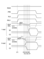
- FIG. 4 is a timing chart showing an example of write operation of the semiconductor memory device according to the first embodiment
- 4 is a timing chart showing an example of read operation of the semiconductor memory device according to the first embodiment
- 3 is a circuit diagram illustrating bit line capacitance in a semiconductor memory device according to a comparative example
- FIG. 3 is a circuit diagram illustrating bit line capacitance in the semiconductor memory device according to the first embodiment
- FIG. FIG. 10 is a diagram showing temporal changes in voltages of bit lines;
- FIG. 10 is a diagram showing temporal changes in voltages of bit lines;
- FIG. 10 is a circuit diagram showing a detailed configuration example of a semiconductor memory device according to a second embodiment; 9 is a timing chart showing an example of write operation of the semiconductor memory device according to the second embodiment; 9 is a timing chart showing an example of read operation of the semiconductor memory device according to the second embodiment; FIG. 11 is a circuit diagram showing a detailed configuration example of a semiconductor memory device according to a third embodiment; FIG. 11 is a timing chart showing an example of write operation of the semiconductor memory device according to the third embodiment; FIG. FIG. 11 is a timing chart showing an example of read operation of the semiconductor memory device according to the third embodiment; FIG. FIG. 11 is a circuit diagram showing a detailed configuration example of a semiconductor memory device according to a fourth embodiment; FIG. 14 is a timing chart showing an example of write operation of the semiconductor memory device according to the fourth embodiment; FIG. FIG. 14 is a timing chart showing an example of read operation of the semiconductor memory device according to the fourth embodiment; FIG.
- the semiconductor memory device may have components and functions that are not illustrated or described. The following description does not exclude components or features not shown or described.
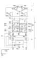
- FIG. 1 is a schematic diagram showing a configuration example of a semiconductor memory device 1 according to the first embodiment. However, FIG. 1 shows the main part of the semiconductor memory device 1 .
- a semiconductor memory device 1 illustrated in FIG. 1 A semiconductor memory device 1 illustrated in FIG.
- the semiconductor memory device 1 has m (rows; rows) ⁇ n (columns; columns) memory cells MC arranged in a matrix in a memory cell array 2 .
- the semiconductor memory device 1 has a function of selecting a desired memory cell MC from among the plurality of memory cells MC, a function of writing data to the selected memory cell MC, and a function of reading data from the selected memory cell MC. have.
- One memory cell MC has a fuse element F as a memory element and stores 1-bit data ("0" or "1"). Note that the fuse element F is simply illustrated in the memory cell MC illustrated in FIG.
- the fuse element F is, for example, an electric fuse element (eFUSE) whose resistance can be electrically irreversibly controlled. In the following description, it is assumed that the fuse element F is an electrical fuse element made of, for example, a polysilicon fuse.
- the low resistance value refers to the initial resistance value before the current is passed through the fuse element F.
- a high resistance value refers to a resistance value after the fuse element F is blown.
- the fuse element F When the fuse element F is blown, its resistance value may match the resistance value of reference resistance elements (first reference resistance element RF1 and second reference resistance element RF2) (see FIG. 2), which will be described later.
- the state (first state) in which the resistance value of the fuse element F is low is also referred to as the "unwritten state” in association with "0".
- the state (second state) in which the resistance value of the fuse element F is high is also referred to as the "write state” in association with "1".
- the memory cell MC stores 1-bit data of "0" or "1” depending on the resistance value of the fuse element F. For this reason, changing the resistance value of the fuse element F from a low resistance value to a high resistance value is also simply referred to as “writing (of the memory cell MC)" or "programming.”
- the fuse element F is biased when the memory cell MC is read. Then, the voltage output to the first read bit line RBLL and the second read bit line RBLR (see FIG. 2) on the bit line BL[n] is compared with the reference voltage to determine the resistance of the fuse element F of the memory cell MC. The value, ie '0' or '1', is read out by the readout circuit 7 .
- the decoder 4 controls the operation of each memory cell MC in the memory cell array 2. Basically, the decoder 4 selects memory cells MC to be read and written.
- the fuse power supply 6 is connected to the bit line BL[n].
- the fuse power supply 6 supplies the fuse element F with a fuse power supply voltage VDDFIL (>power supply voltage VDD) for biasing the fuse element F when the memory cell MC is written.
- VDDFIL fuse power supply voltage
- the read circuit 7 has, for example, a function of selecting the bit line BL[n], a comparison section 72 (see FIG. 2), and a reference voltage generation section 71 (see FIG. 2).
- the read circuit 7 reads data from a read target memory cell MC at the time of reading.
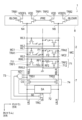
- FIG. 2 is a circuit diagram showing a detailed configuration example of the semiconductor memory device according to the first embodiment.
- the bit line BL[n] includes a first read bit line RBLL, a second read bit line RBLR, and a write bit line WBL.
- a first read bit line (first voltage supply line) RBLL supplies a predetermined voltage (first voltage) so that the fuse element F and the reference resistance element can be biased. Bias is, for example, voltage application.
- the fuse element F includes a first fuse element F1 and a second fuse element F2 shown in FIG.
- the reference resistance elements include a first reference resistance element RF1 and a second reference resistance element RF2 shown in FIG.
- the second read bit line (third voltage supply line) RBLR supplies the first voltage so that the fuse element F and the reference resistance element can be biased.
- a write bit line (second voltage supply line) WBL supplies a predetermined voltage (second voltage) different from the first voltage so that the fuse element F and the reference resistor element can be biased.
- the first voltage in the write operation is, for example, the ground voltage (0 V).
- the second voltage in the write operation is, for example, the fuse power supply voltage VDDFIL. Therefore, in a write operation, the first voltage is lower than the second voltage.
- the first voltage in the read operation is, for example, the power supply voltage (reference voltage) VDD.
- the second voltage in the read operation is, for example, the ground voltage. Therefore, in a read operation, the first voltage is higher than the second voltage.
- the second voltage (fuse power supply voltage VDDFIL) in the write operation is higher than the first voltage (power supply voltage VDD) in the read operation.
- the fuse power supply voltage VDDFIL is, for example, about 1.8V.
- the power supply voltage VDD is, for example, about 0.8V.
- the memory cell MC has a first memory cell MC1 and a second memory cell MC2.
- the first memory cell MC1 is arranged in the left column of the two columns of memory cells MC shown in FIG.
- the second memory cell MC2 is arranged in the right column of the two columns of memory cells MC shown in FIG.
- FIG. 2 exemplifies a case where four memory cells MC are arranged in two columns (2 bits) ⁇ 2 rows (2 rows). is not limited to, and may be, for example, one line. In the following, unless otherwise specified, it is assumed that a plurality of memory cells MC are arranged in a plurality of columns and a plurality of rows.
- first memory cells MC1 and the number of second memory cells MC2 are the same.
- the first memory cell MC1 and the second memory cell MC2 are arranged substantially symmetrically (for example, substantially left-right symmetrically) with the write bit line WBL interposed therebetween.
- the first read bit line RBLL and the second read bit line RBLR have substantially the same capacitance.
- the first memory cells MC1 and the second memory cells MC2 arranged in two columns are configured as one unit.
- the first memory cells MC1 and the second memory cells MC2 arranged in two columns may be arranged in plural units in the row direction.
- FIG. 2 A configuration in which a plurality of memory cells MC are arranged in the column direction is hereinafter referred to as a bit configuration.
- FIG. 2 exemplifies one bit configuration in two columns. However, other bit configurations do not necessarily have to be the same configurations. In addition, below, one bit configuration will be described assuming that a plurality of bit configurations have the same configuration.
- the first memory cell MC1 has a first fuse element F1 and a first access transistor TRA1.
- a first fuse element (first memory element) F1 is connected between a first read bit line RBLL (first access transistor TRA1) and a write bit line WBL.
- the first fuse element F1 has a resistance value according to the first state or the second state.
- a first access transistor (first cell transistor) TRA1 is connected between the first fuse element F1 and the first read bit line RBLL. Therefore, the first fuse element F1 is not directly connected to the first read bit line RBLL, but is connected to the first read bit line RBLL via the first access transistor TRA1. This allows the read operation to be performed more appropriately, as will be described later.
- the gates of the first access transistor TRA1 are connected to word lines WL1, WL3, .
- the first fuse element F1 is biased by the fuse power supply voltage VDDFIL or the power supply voltage VDD.
- the first access transistor TRA1 is, for example, an NMOS (n-channel Metal Oxide Semiconductor) transistor.
- the first fuse element F1 and the first access transistor TRA1 are connected in series.
- the second memory cell MC2 has a second fuse element F2 and a second access transistor TRA2.
- the second fuse element (second memory element) F2 is connected between the write bit line WBL and the second read bit line RBLR (second access transistor TRA2).
- the second fuse element F2 has a resistance value according to the first state or the second state.
- a second access transistor (second cell transistor) TRA2 is connected between the second fuse element F2 and the second read bit line RBLR. Therefore, the second fuse element F2 is connected to the second read bit line RBLR through the second access transistor TRA2 without being directly connected to the second read bit line RBLR. This allows the read operation to be performed more appropriately, as will be described later.
- the gates of the second access transistors TRA2 are connected to the word lines WL0, WL2, .
- the second fuse element F2 is biased by the fuse power supply voltage VDDFIL or the power supply voltage VDD.
- the second access transistor TRA2 is, for example, an NMOS transistor.
- the second fuse element F2 and the second access transistor TRA2 are connected in series.
- the semiconductor memory device of this embodiment has a plurality of word lines WL0, WL1, WL2, . . . extending in the row direction.
- Each word line WL0, WL1, WL2, . . . turns on or off the first access transistor TRA1 and the second access transistor TRA2 in each memory cell MC.
- word lines WL0 and WL2 turn on or off the second access transistor TRA2 of the right second memory cell MC2.
- the word lines WL1 and WL3 turn on or off the first access transistor TRA1 of the left first memory cell MC1.
- the readout circuit 7 has a reference voltage generator 71 , a comparator 72 , a comparison controller 73 , and a bit line separator 74 .
- the comparison unit 72 may also be called a sense amplifier (SA).
- the reference voltage generator 71 generates a reference voltage that is compared with the voltage generated by biasing the fuse element F in the read operation.
- the reference voltage is a voltage generated by biasing the first fuse element F1 and the second fuse element F2, which have resistance values corresponding to the first state, based on the first voltage and the second voltage, and a reference voltage corresponding to the second state. and a voltage that the first fuse element F1 and the second fuse element F2 having the same resistance are biased based on the first voltage and the second voltage.
- the reference voltage generator 71 has a first reference voltage generator 711 and a second reference voltage generator 712 .
- the first reference voltage generator 711 is connected between the first read bit line RBLL and the write bit line WBL.
- the first reference voltage generator 711 generates a reference voltage when the second memory cell MC2 is read.
- the second reference voltage generator 712 is connected between the write bit line WBL and the second read bit line RBLR.
- the second reference voltage generator 712 generates a reference voltage when the read operation of the first memory cell MC1 is performed.
- the first reference voltage generator 711 and the second reference voltage generator 712 are arranged substantially symmetrically (for example, substantially left-right symmetrically) with the write bit line WBL interposed therebetween.
- the first reference voltage generator 711 has a first reference resistance element RF1 and a first reference transistor TRF1.
- the first reference resistance element RF1 is connected between the first read bit line RBLL (first reference transistor TRF1) and the write bit line WBL.
- the first reference transistor TRF1 is connected between the first reference resistance element RF1 and the first read bit line RBLL. Therefore, the first reference resistive element RF1 is not directly connected to the first read bit line RBLL, but is connected to the first read bit line RBLL via the first reference transistor TRF1.
- the gate of the first reference transistor TRF1 is connected to the word line RWL1.
- the first reference resistor element RF1 is biased by the power supply voltage VDD.
- the first reference transistor TRF1 is, for example, an NMOS transistor.
- the first reference resistive element RF1 and the first reference transistor TRF1 are connected in series.
- the second reference voltage generator 712 has a second reference resistor element RF2 and a second reference transistor TRF2.
- the second reference resistance element RF2 is connected between the write bit line WBL and the second read bit line RBLR (second reference transistor TRF2).
- the second reference transistor TRF2 is connected between the second reference resistance element RF2 and the second read bit line RBLR. Therefore, the second reference resistance element RF2 is not directly connected to the second read bit line RBLR, but is connected to the second read bit line RBLR via the second reference transistor TRF2.
- the gate of the second reference transistor TRF2 is connected to the word line RWL0.
- the second reference resistance element RF2 is biased by the power supply voltage VDD.
- the second reference transistor TRF2 is, for example, an NMOS transistor.
- the second reference resistive element RF2 and the second reference transistor TRF2 are connected in series.
- the first reference resistor element RF1, the second reference resistor element RF2, the first reference transistor TRF1, and the second reference transistor TRF2 are arranged substantially symmetrically across the write bit line WBL.
- first reference resistance element RF1 and the second reference resistance element RF2 have substantially the same resistance value, for example.
- the comparator 72 compares the reference voltage with the voltage generated by biasing the first fuse element F1 or the second fuse element F2 with the first voltage and the second voltage. More specifically, the comparator 72 compares the voltage of the first read bit line RBLL and the voltage of the second read bit line RBLR. That is, when reading the first memory cell MC1, the decoder 4 selects the first memory cell MC1 and the second reference voltage generator 712, and the comparator 72 compares the voltages of the two bit lines. When reading the second memory cell MC2, the decoder 4 selects the second memory cell MC2 and the first reference voltage generator 711, and the comparator 72 compares the voltages of the two bit lines. Thereby, the resistance value of the fuse element F of the memory cell MC to be read, that is, the unwritten state (“0”) or the written state (“1”) is read. More specifically, the comparator 72 amplifies and compares the potential difference between the two bit lines.
- the comparison control section 73 causes the comparison section 72 to start comparison at timing according to the voltages of the first read bit line RBLL and the second read bit line RBLR.
- the comparison control section 73 has a NAND circuit ND1 and a comparison control transistor TRC.
- Two inputs of the NAND circuit ND1 are electrically connected to the first read bit line RBLL and the second read bit line RBLR.
- the output of the NAND circuit ND1 is electrically connected to the gate of the comparison control transistor TRC.
- the NAND circuit ND1 outputs a high signal when the voltage of at least one of the first read bit line RBLL and the second read bit line RBLR is lower than the first predetermined value.
- the comparison control transistor TRC is connected between the comparison section 72 and the ground.
- the gate of the comparison control transistor TRC is connected to the output of the NAND circuit ND1 and receives the signal SE. Outputting a high signal SE from the NAND circuit ND1 turns on the comparison control transistor TRC.
- the comparison control transistor TRC causes the comparison unit 72 to start comparison by turning it on.
- the bit line isolation section 74 electrically isolates the bit lines. As a result, when the comparison unit 72 amplifies the potential difference, it is possible to suppress the influence of the capacitance of the bit line. As a result, power consumption can be suppressed.
- the bit line isolation section 74 has a first isolation transistor TRS1 and a second isolation transistor TRS2.
- the first isolation transistor TRS1 is connected between the first read bit line RBLL and the first isolation read bit line LBLL.
- a signal CS is input to the gate of the first separation transistor TRS1.
- the first isolation transistor TRS1 electrically connects the first read bit line RBLL and the first isolation read bit line LBLL when turned on, and electrically connects the first read bit line RBLL and the first isolation read when turned off.
- the bit line LBLL is electrically disconnected.
- the first isolation transistor TRS1 is, for example, an NMOS transistor.
- the signal CS has a signal level corresponding to the signal level of the signal SE output from the NAND circuit ND1 through wiring (not shown), for example.
- the second isolation transistor TRS2 is connected between the second read bit line RBLR and the second isolation read bit line LBLR.
- a signal CS is input to the gate of the second separation transistor TRS2.
- the second isolation transistor TRS2 electrically connects the second read bit line RBLR and the second isolation read bit line LBLR when turned on, and electrically connects the second read bit line RBLR and the second isolation read line when turned off.
- the bit line LBLR is electrically disconnected.
- the second isolation transistor TRS2 is, for example, an NMOS transistor.
- the semiconductor memory device 1 further includes a voltage supply section 8 .
- the voltage supply unit 8 is omitted in FIG.
- Voltage supply unit 8 is connected between fuse power supply 6 and memory cell array 2 .
- the voltage supply unit 8 controls voltage supply by the write bit line WBL, the first read bit line RBLL, and the second read bit line RBLR.
- the operation of the voltage supply section 8 is controlled by the decoder 4, for example.
- the voltage supply unit 8 has a first blow transistor TRB1, a second blow transistor TRB2, a third blow transistor TRB3, a read transistor TRR, a first precharge transistor TRP1, and a second precharge transistor TRP2. .
- the first blow transistor TRB1 is connected between the node N1 and the ground.
- the node N1 is provided between the power supply voltage node VDD (first precharge transistor TRP1) and the memory cell array 2 on the first read bit line RBLL.
- a BLOW signal is input to the gate of the first blow transistor TRB1.
- the write operation of the first memory cell MC1 is performed by turning on the first blow transistor TRB1.
- the first blow transistor TRB1 is, for example, an NMOS transistor.
- the second blow transistor TRB2 is connected between the node N2 and the ground.
- the node N2 is provided between the power supply voltage node VDD (second precharge transistor TRP2) and the memory cell array 2 on the second read bit line RBLR.
- a BLOW signal is input to the gate of the second blow transistor TRB2.
- the write operation of the second memory cell MC2 is performed by turning on the second blow transistor TRB2.
- the second blow transistor TRB2 is, for example, an NMOS transistor.
- the third blow transistor TRB3 is connected between the node N3 and the fuse power supply voltage node VDDFIL. Node N3 is provided between fuse power supply voltage node VDDFIL and memory cell array 2 on write bit line WBL.
- a /BLOW signal is input to the gate of the third blow transistor TRB3.
- the write operation of the first memory cell MC1 or the second memory cell MC2 is performed by turning on the third blow transistor TRB3.
- the third blow transistor TRB3 is, for example, a PMOS (p-channel Metal Oxide Semiconductor) transistor.
- the read transistor TRR is connected between the node N3 and the ground. Node N3 is provided between fuse power supply voltage node VDDFIL (third blow transistor TRB3) and memory cell array 2 on write bit line WBL. A READ signal is input to the gate of the read transistor TRR. The read operation of the first memory cell MC1 or the second memory cell MC2 is performed by turning on the read transistor TRR.
- the read transistor TRR is, for example, an NMOS transistor.
- the first precharge transistor TRP1 is connected between the power supply voltage node VDD and the memory cell array 2 (node N1). A /PRE signal is input to the gate of the first precharge transistor TRP1. By turning on the first precharge transistor TRP1, the first read bit line RBLL is precharged in the read operation. Details of the precharge will be described later with reference to FIG.
- the first precharge transistor TRP1 is, for example, a PMOS transistor.
- the second precharge transistor TRP2 is connected between the power supply voltage node VDD and the memory cell array 2 (node N2). A /PRE signal is input to the gate of the second precharge transistor TRP2. By turning on the second precharge transistor TRP2, the second read bit line RBLR is precharged in the read operation. Details of the precharge will be described later with reference to FIG.
- the second precharge transistor TRP2 is, for example, a PMOS transistor.
- FIG. 3 is a timing chart showing an example of write operation of the semiconductor memory device according to the first embodiment.
- FIG. 3 shows a timing chart of the write operation of the second memory cell MC2.
- the BLOW signal In the initial state, the BLOW signal is in a high state. Therefore, the first blow transistor TRB1 and the second blow transistor TRB2 are on. The /BLOW signal is in a high state. Therefore, the third blow transistor TRB3 is off. The signals on word lines WL0 and RWL1 are in the low state. Therefore, the second access transistor TRA2 and the first reference transistor TRF1 are off.
- the signal on word line WL0 becomes high. This turns on the second access transistor TRA2.
- the /BLOW signal goes low. This turns on the third blow transistor TRB3. As a result, the voltage of the write bit line WBL rises, and the second fuse element F2 is biased by the fuse power supply voltage VDDFIL to enter the write state.
- the signal SE is in a low state during the write operation. Therefore, comparison control transistor TRC is in an off state. Signal CS is in the low state. Therefore, the first isolation transistor TRS1 and the second isolation transistor TRS2 are off. That is, the first read bit line RBLL and the second read bit line RBLR are electrically disconnected from the first separated read bit line LBLL and the second separated read bit line LBLR, respectively.
- the read transistor TRR, the first precharge transistor TRP1, and the second precharge transistor TRP2 are in the off state during the write operation.
- FIG. 4 is a timing chart showing an example of read operation of the semiconductor memory device according to the first embodiment.
- FIG. 4 shows a timing chart of the read operation of the second memory cell MC2.
- the voltage supply unit 8 supplies the first voltage to the first read bit line RBLL and the second read bit line RBLR in advance, and preliminarily supplies the write bit line RBLL with the first voltage.
- the voltage supply unit 8 stops supplying the first voltage to the first read bit line RBLL and the second read bit line RBLR.
- the decoder (cell transistor control unit) 4 controls the first access transistor TRA1 of the first memory cell MC1 to be read or the first access transistor TRA1 of the second memory cell MC2 to be read. 2 Turn on the access transistor TRA2. In this manner, charge extraction is performed.
- the READ signal In the initial state, the READ signal is in a high state. Therefore, the read transistor TRR is on. As a result, the write bit line WBL is discharged to 0V, for example.
- the /PRE signal is in the low state. Therefore, the first precharge transistor TRP1 and the second precharge transistor TRP2 are on.
- the signals on word lines WL0 and RWL1 are in the low state. Therefore, the second access transistor TRA2 and the first reference transistor TRF1 are off.
- the signal SE is in a low state. Therefore, comparison control transistor TRC is in an off state. Signal CS is in a high state. Therefore, the first isolation transistor TRS1 and the second isolation transistor TRS2 are on. That is, the first read bit line RBLL and the second read bit line RBLR are electrically connected to the first separated read bit line LBLL and the second separated read bit line LBLR, respectively.
- the voltages of the first separated read bit line LBLL (first read bit line RBLL) and the second separated read bit line LBLR (second read bit line RBLR) are precharged to the power supply voltage VDD.
- All first access transistors TRA1, all second access transistors TRA2, first reference transistors TRF1 and second reference transistors TRF2 shown in FIG. 2 are in an off state. Therefore, regardless of whether the state of the memory cell MC is in the written state (“1”) or in the unwritten state (“0”), the electric charge does not escape from the first separation read bit line LBLL. and stored in the second separated read bit line LBLR.
- the /PRE signal becomes high.
- the first precharge transistor TRP1 and the second precharge transistor TRP2 are turned off.
- the signals on word lines WL0 and RWL1 go high substantially at the same time.
- the second access transistor TRA2 and the first reference transistor TRF1 are turned on substantially simultaneously.
- the voltages of the first separated read bit line LBLL and the second separated read bit line LBLR drop. This is because the charges accumulated in the first separated read bit line LBLL and the second separated read bit line LBLR flow through the write bit line WBL.
- a current flowing through the write bit line WBL flows to the ground connected to the source of the read transistor TRR.
- the voltage drop speed differs between the first separated read bit line LBLL and the second separated read bit line LBLR.
- the rate of decrease in the voltage of the first separated read bit line LBLL is determined by the resistance value of the first reference resistance element RF1. Therefore, the voltage drop speed of the first separated read bit line LBLL does not change depending on the state (0/1) of the second fuse element F2 of the second memory cell MC2.
- the voltage drop speed of the second separated read bit line LBLR changes depending on the state (0/1) of the second fuse element F2 of the second memory cell MC2.
- the voltage drop speed of the second separation read bit line LBLR is equal to that of the first separation read bit line. It is slower than the voltage drop rate of LBLL.
- the voltage of the first separated read bit line LBLL becomes lower than the logic threshold (first predetermined value) of the NAND circuit ND1.
- the NAND circuit ND1 inputs the signal SE that changes from low to high to the gate of the comparison control transistor TRC.
- the signal CS becomes low at time t17 due to the signal SE becoming high.
- the first isolation transistor TRS1 and the second isolation transistor TRS2 are turned off.
- the first read bit line RBLL and the second read bit line RBLR are electrically disconnected from the first separated read bit line LBLL and the second separated read bit line LBLR, respectively.
- the comparator 72 performs voltage comparison by turning on the comparison control transistor TRC. That is, the comparison control section 73 causes the comparison section 72 to start comparison at the timing when the voltage of at least one of the first read bit line RBLL and the second read bit line RBLR becomes lower than the first predetermined value. After time t16, the comparator 72 amplifies and compares the potential difference between the first separated read bit line LBLL and the second separated read bit line LBLR.
- the /PRE signal goes low, and the signals on word lines WL0 and RWL1 go low.
- the first precharge transistor TRP1 and the second precharge transistor TRP2 are turned on, and the second access transistor TRA2 and the first reference transistor TRF1 are turned off.
- the voltage drop speed of the second separation read bit line LBLR is equal to that of the first separation read bit line. Faster than the LBLL voltage drop rate.
- the voltage of the second separated read bit line LBLR becomes lower than the logic threshold (first predetermined value) of the NAND circuit ND1.
- the NAND circuit ND1 inputs the signal SE that changes from low to high to the gate of the comparison control transistor TRC.
- the signal CS becomes low at time t14 due to the signal SE becoming high.
- the first isolation transistor TRS1 and the second isolation transistor TRS2 are turned off.
- the first read bit line RBLL and the second read bit line RBLR are electrically disconnected from the first separated read bit line LBLL and the second separated read bit line LBLR, respectively.
- the comparator 72 compares the voltages by turning on the comparison control transistor TRC. That is, the comparison control section 73 causes the comparison section 72 to start comparison at the timing when the voltage of at least one of the first read bit line RBLL and the second read bit line RBLR becomes lower than the first predetermined value. After time t13, the comparator 72 amplifies and compares the potential difference between the first separated read bit line LBLL and the second separated read bit line LBLR.
- the /PRE signal goes low, and the signals on word lines WL0 and RWL1 go low.
- the first precharge transistor TRP1 and the second precharge transistor TRP2 are turned on, and the second access transistor TRA2 and the first reference transistor TRF1 are turned off.
- the comparison start timing by the comparator 72 differs depending on the state (0/1) of the second memory cell MC2. That is, the timing from the rise of the voltage of the word line to the activation of the sense amplifier is set so that the logic threshold value (first predetermined value) of the NAND circuit ND1 of the first separated read bit line LBLL and the second separated read bit line LBLR precedes. is determined in a self-consistent manner at a rate lower than .
- the BLOW signal and the /BLOW signal are not shown in FIG. 4, the first blow transistor TRB1, the second blow transistor TRB2 and the third blow transistor TRB3 are in the off state.
- the first memory cell MC1 is connected between the first read bit line RBLL and the write bit line WBL.
- the first access transistor TRA1 is connected between the first fuse element F1 and the first read bit line RBLL.
- the second memory cell MC2 is connected between the write bit line WBL and the second read bit line RBLR.
- the second access transistor TRA2 is connected between the second fuse element F2 and the second read bit line RBLR.
- connection relationship (placement) between the first reference transistor TRF1 and the second reference transistor TRF2 corresponds to the connection relationship between the first access transistor TRA1 and the second access transistor TRA2.
- the first reference transistor may be connected between the first reference resistance element RF1 and the write bit line WBL.
- the second reference resistance element RF2 may be connected between the second reference resistance element RF2 and the write bit line WBL.
- FIG. 5 is a circuit diagram illustrating bit line capacitance in a semiconductor memory device 1a according to a comparative example.
- FIG. 6 is a circuit diagram illustrating bit line capacitance in the semiconductor memory device 1 according to the first embodiment.
- the comparative example differs from the first embodiment in the arrangement of fuse elements and access transistors in memory cells MC. Note that in FIG. 5, a first bit line BLL and a second bit line BLR are provided instead of the first read bit line RBLL and the second read bit line RBLR. Similarly, instead of write bit line WBL, ground line GND is provided.
- the first access transistor TRA1 of the first memory cell MC1 is connected between the first fuse element F1 and the ground line GND. Therefore, the first fuse element F1 is directly connected to the first bit line BLL.
- the second access transistor TRA2 of the second memory cell MC2 is connected between the second fuse element F2 and the ground line GND. Therefore, the second fuse element F2 is directly connected to the second bit line BLR.
- the total capacitance of the first bit lines BLL shown in FIG. 5 is expressed by Equation 1 using the bit line wiring capacitance of the first bit lines BLL.
- Total capacitance Bit line wiring capacitance (Formula 1)
- the total capacitance of the second bit line BLR shown in FIG. 5 is calculated using the bit line wiring capacitance of the second bit line BLR, the fuse element capacitance of the second fuse element F2, and the transistor diffusion capacitance of the second access transistor TRA2. It is represented by Formula 2.
- Total capacity bit line wiring capacity + (fuse element capacity + transistor diffusion capacity) x number of bits (formula 2)
- the total capacitance of the second bit lines BLR is greater than the total capacitance of the first bit lines BLL.
- the time to pull out the precharged charge in the bit lines also depends on the write data pattern. It may change significantly. In this case, in the comparative example, it may be difficult to stably perform the read operation using the precharge shown in FIG.
- the total capacitance of each of the first read bit line RBLL and the second read bit line RBLR is substantially constant regardless of the write data pattern. Therefore, the time for extracting the charges precharged in the bit line (the rate at which the voltage of the bit line drops) is also substantially constant regardless of the write data pattern. As a result, the read operation using precharge can be performed more stably.
- FIG. 7 is a diagram showing temporal changes in the voltage of the bit line.
- the upper part of FIG. 7 is a graph showing the time change of the voltage of the word line.
- the middle part of FIG. 7 is a graph showing the time change of the bit line voltage in the comparative example.
- the lower part of FIG. 7 is a graph showing the time change of the bit line voltage in the first embodiment.
- the vertical axis of the graph shown in FIG. 7 is voltage.
- the horizontal axis of the graph shown in FIG. 7 is time. Note that the time shown on the horizontal axis is common to all graphs.
- the word line voltage includes, for example, word lines RWL0, RWL1, WL0, and WL1.
- Bit line voltages Vb0 and Vb1 of bit lines electrically connected to memory cells MC are indicated by solid lines.
- a bit line voltage Vb0 indicates a voltage when the memory cell MC is in an unwritten state.
- a bit line voltage Vb1 indicates a voltage when the memory cell MC is in the write state.
- the reference voltage Vref of the reference bit line electrically connected to the reference voltage generator 71 is indicated by a dashed line.
- bit line and reference bit line in the comparative example correspond to the second bit line BLR and first bit line BLL shown in FIG. 5, respectively.
- a bit line and a reference bit line in the first embodiment correspond to the second read bit line RBLR and the first read bit line RBLL shown in FIG. 6, respectively.
- the word line voltage is low in the initial state.
- the word line voltage becomes High at time ta. This activates the word line.
- the second fuse element F2 is biased by the power supply voltage VDD and DC current continues to flow through the second fuse element F2.
- bit line voltages Vb0 and Vb1 and the reference voltage Vref are zero, for example.
- bit line voltages Vb0 and Vb1 and the reference voltage Vref rise. Since the fuse element is blown, the bit line voltage Vb1 is higher than the bit line voltage Vb0, and it takes time to stabilize the voltage.
- bit line voltage Vb1 exceeds the reference voltage Vref. That is, after time tc, reference voltage Vref attains a voltage level between bit line voltage Vb0 and bit line voltage Vb1. Therefore, in the comparative example, it is necessary for the comparison unit 72 to perform the comparison after sufficiently waiting until at least the time tc has passed.
- temporal changes of the bit line voltages Vb0 and Vb1 and the reference voltage Vref in the comparative example are examples.
- bit line voltages Vb0 and Vb1 and the reference voltage Vref are precharged to the power supply voltage VDD.
- the word line voltage becomes high. Also, at time ta, the bit line voltages Vb0 and Vb1 and the reference voltage Vref decrease. This is because the first access transistor TRA1 and the second access transistor TRA2 are turned on, and charges are extracted from the first read bit line RBLL and the second read bit line RBLR.
- the rate of decrease of reference voltage Vref after time ta is between the rate of decrease of bit line voltage Vb0 and the rate of decrease of bit line voltage Vb1.
- the access transistor is arranged between the fuse element and the read bit line. As a result, it is possible to suppress variations in the change speed (decrease speed) of the voltage of the bit line when the charge is extracted, depending on the pattern of the write data. As a result, the read operation can be stably performed. Also, as shown in FIG.
- the potential difference between the bit line voltages Vb0 and Vb1 and the reference voltage Vref widens faster than in the comparative example.
- the time from word line activation to sense amplifier activation can be shortened.
- high-speed read operation becomes possible.
- the potential difference between the bit line voltages Vb0 and Vb1 and the reference voltage Vref is generated in a relatively short time after the word line is activated due to the difference in the speed of extracting electric charges. is occurring. Since the speed at which electric charges are extracted is caused by the difference in resistance values, there is a possibility that a sufficient potential difference can be obtained regardless of the magnitude of the precharge voltage at the start of reading. For example, the power supply voltage VDD can be lowered within a range in which the comparing section 72 can appropriately perform comparison. Thereby, the voltage can be lowered.
- the potential difference between the first voltage and the second voltage is between the first read bit line RBLL and the second read bit line RBLR after the decoder 4 turns on the first access transistor TRA1 or the second access transistor TRA2. is the potential difference corresponding to the difference in the voltage change rate of
- FIG. 8 is a circuit diagram showing a detailed configuration example of the semiconductor memory device 1 according to the second embodiment.
- the second embodiment differs from the first embodiment in that the write bit line WBL is grounded.
- the write bit line WBL in the second embodiment corresponds to the ground line GND in the comparative example.
- the first voltage in the write operation is, for example, the fuse power supply voltage VDDFIL.
- the second voltage in the write operation is, for example, the ground voltage (0V). Therefore, in a write operation, the first voltage is higher than the second voltage.
- the first voltage in the read operation is, for example, power supply voltage VDD.
- the second voltage in the read operation is, for example, the ground voltage. Therefore, in a read operation, the first voltage is higher than the second voltage.
- the first voltage (fuse power supply voltage VDDFIL) in the write operation is higher than the first voltage (power supply voltage VDD) in the read operation.
- the voltage supply section 8 in the second embodiment does not have the third blow transistor TRB3 and the read transistor TRR, unlike the first embodiment.
- the first blow transistor TRB1 is connected between the node N4 on the first read bit line RBLL and the fuse power supply voltage node VDDFIL.
- a /BLOWL signal is input to the gate of the first blow transistor TRB1.
- the first blow transistor TRB1 is, for example, a PMOS transistor.
- the second blow transistor TRB2 is connected between the node N5 on the second read bit line RBLR and the fuse power supply voltage node VDDFIL.
- a /BLOWR signal is input to the gate of the second blow transistor TRB2.
- the second blow transistor TRB2 is, for example, a PMOS transistor.
- the first precharge transistor TRP1 is connected between the node N4 on the first read bit line RBLL and the power supply voltage node VDD.
- the second precharge transistor TRP2 is connected between the node N5 on the second read bit line RBLR and the power supply voltage node VDD.
- the write bit line WBL is connected to the ground and fixed at the ground voltage. That is, the voltage supply unit 8 fixes the write bit line WBL to the second voltage (ground voltage).
- FIG. 9 is a timing chart showing an example of write operation of the semiconductor memory device 1 according to the second embodiment.
- the /BLOWL signal and /BLOWR signal are in a high state. Therefore, the first blow transistor TRB1 and the second blow transistor TRB2 are off.
- the signals on word lines WL0 and RWL1 are in the low state. Therefore, the second access transistor TRA2 and the first reference transistor TRF1 are off.
- the signal on word line WL0 becomes high. This turns on the second access transistor TRA2.
- the /BLOWR signal goes low. This turns on the second blow transistor TRB2. As a result, the voltage of the second read bit line RBLR rises, and the second fuse element F2 is biased by the fuse power supply voltage VDDFIL to enter the write state.
- the /BLOWR signal goes high and the signal on word line WL0 goes low.
- the second blow transistor TRB2 is turned off, and the second access transistor TRA2 is turned off.
- FIG. 10 is a timing chart showing an example of read operation of the semiconductor memory device 1 according to the second embodiment.
- the READ signal is not input.
- Other read operations of the semiconductor memory device 1 according to the second embodiment are the same as in FIG. 4 described in the first embodiment.
- the write bit line WBL may be grounded as in the second embodiment. Also in this case, the same effect as in the first embodiment can be obtained.
- FIG. 11 is a circuit diagram showing a detailed configuration example of the semiconductor memory device 1 according to the third embodiment.
- the third embodiment differs from the first embodiment in that the precharge level of the first read bit line RBLL and the second read bit line RBLR is 0V.
- the first voltage in the write operation is, for example, the ground voltage (0 V).
- the second voltage in the write operation is, for example, the fuse power supply voltage VDDFIL. Therefore, in a write operation, the first voltage is lower than the second voltage.
- the first voltage in the read operation is, for example, the ground voltage.
- the second voltage in the read operation is, for example, power supply voltage VDD. Therefore, in a read operation, the first voltage is lower than the second voltage.
- the second voltage (fuse power supply voltage VDDFIL) in the write operation is higher than the second voltage (power supply voltage VDD) in the read operation.
- the voltage supply section 8 in the third embodiment does not have the first blow transistor TRB1 and the second blow transistor TRB2.
- the third blow transistor TRB3 is connected between the node N6 on the write bit line WBL and the fuse power supply voltage node VDDFIL.
- the read transistor TRR is connected between the node N6 on the write bit line WBL and the power supply voltage node VDD.
- a /READ signal is input to the gate of the read transistor TRR.
- the read transistor TRR is, for example, a PMOS transistor.
- the first precharge transistor TRP1 is connected between one end of the first read bit line RBLL and the ground.
- a PRE signal is input to the gate of the first precharge transistor TRP1.
- the first precharge transistor TRP1 is, for example, an NMOS transistor.
- the second precharge transistor TRP2 is connected between one end of the second read bit line RBLR and the ground.
- a PRE signal is input to the gate of the second precharge transistor TRP2.
- the second precharge transistor TRP2 is, for example, an NMOS transistor.
- the comparison control unit 73 has an OR circuit OR1 instead of the NAND circuit ND1 in the first embodiment.
- Two inputs of the OR circuit OR1 are electrically connected to the first read bit line RBLL and the second read bit line RBLR.
- the output of the OR circuit OR1 is electrically connected to the gate of the comparison control transistor TRC.
- the OR circuit OR1 outputs a high signal when the voltage of at least one of the first read bit line RBLL and the second read bit line RBLR is higher than the second predetermined value.
- FIG. 12 is a timing chart showing a write operation example of the semiconductor memory device 1 according to the third embodiment.
- the PRE signal In the initial state, the PRE signal is in a high state. Therefore, the first precharge transistor TRP1 and the second precharge transistor TRP2 are on.
- the first precharge transistor TRP1 and the second precharge transistor TRP2 operate in substantially the same manner as the first blow transistor TRB1 and the second blow transistor TRB2 in the first embodiment.
- Other operations of the semiconductor memory device 1 according to the third embodiment are the same as in FIG. 3 described in the first embodiment.
- FIG. 13 is a timing chart showing an example of read operation of the semiconductor memory device 1 according to the third embodiment.
- the /READ signal In the initial state, the /READ signal is in a low state. Therefore, the read transistor TRR is on. As a result, the write bit line WBL is precharged to the power supply voltage VDD. All the first access transistors TRA1, all the second access transistors TRA2, the first reference transistors TRF1 and the second reference transistors TRF2 shown in FIG. 11 are in the off state. Therefore, regardless of whether the memory cell MC is in the written state (“1”) or in the unwritten state (“0”), the charge is accumulated in the write bit line WBL without being discharged. be.
- the PRE signal In the initial state, the PRE signal is in a high state. Therefore, the first precharge transistor TRP1 and the second precharge transistor TRP2 are on. As a result, the voltages of the first read bit line RBLL (first separated read bit line LBLL) and the second read bit line RBLR (second separated read bit line LBLR) are discharged to 0V, for example.
- the PRE signal becomes low.
- the first precharge transistor TRP1 and the second precharge transistor TRP2 are turned off.
- the signals on word lines WL0 and RWL1 go high substantially at the same time.
- the second access transistor TRA2 and the first reference transistor TRF1 are turned on substantially simultaneously.
- the voltages of the first separated read bit line LBLL and the second separated read bit line LBLR rise. This is because the first separated read bit line LBLL and the second separated read bit line LBLR discharged to 0V are charged to the level of the power supply voltage VDD through the read transistor TRR and the write bit line WBL.
- the voltage rise speed differs between the first separated read bit line LBLL and the second separated read bit line LBLR.
- the rate of increase in the voltage of the first separated read bit line LBLL is determined by the resistance value of the first reference resistance element RF1. Therefore, the voltage rising speed of the first separated read bit line LBLL does not change depending on the state (0/1) of the second fuse element F2 of the second memory cell MC2.
- the rate of increase of the voltage of the second separated read bit line LBLR changes depending on the state (0/1) of the second fuse element F2 included in the second memory cell MC2.
- the rate of increase of the voltage of the second separated read bit line LBLR is equal to that of the first separated read bit line. Slower than the LBLL voltage rise rate.
- the voltage of the first separated read bit line LBLL becomes higher than the logic threshold (second predetermined value) of the OR circuit OR1.
- the OR circuit OR1 inputs the signal SE that changes from low to high to the gate of the comparison control transistor TRC.
- the signal CS becomes low at time t54 due to the signal SE becoming high.
- the first isolation transistor TRS1 and the second isolation transistor TRS2 are turned off.
- the first read bit line RBLL and the second read bit line RBLR are electrically disconnected from the first separated read bit line LBLL and the second separated read bit line LBLR, respectively.
- the comparator 72 compares the voltages by turning on the comparison control transistor TRC. That is, the comparison control section 73 causes the comparison section 72 to start comparison at the timing when the voltage of at least one of the first read bit line RBLL and the second read bit line RBLR becomes higher than the second predetermined value. After time t53, the comparator 72 amplifies and compares the potential difference between the first separated read bit line LBLL and the second separated read bit line LBLR.
- the PRE signal goes high, and the signals on word lines WL0 and RWL1 go low.
- the first precharge transistor TRP1 and the second precharge transistor TRP2 are turned on, and the second access transistor TRA2 and the first reference transistor TRF1 are turned off.
- the rate of increase of the voltage of the second separated read bit line LBLR is equal to that of the first separated read bit line. It is faster than the rising speed of the voltage of LBLL.
- the voltage of the second separated read bit line LBLR becomes higher than the logic threshold (second predetermined value) of the OR circuit OR1.
- the OR circuit OR1 inputs the signal SE that changes from low to high to the gate of the comparison control transistor TRC.
- the signal CS becomes low at time t57 due to the signal SE becoming high.
- the first isolation transistor TRS1 and the second isolation transistor TRS2 are turned off.
- the first read bit line RBLL and the second read bit line RBLR are electrically disconnected from the first separated read bit line LBLL and the second separated read bit line LBLR, respectively.
- the comparator 72 compares the voltages by turning on the comparison control transistor TRC. That is, the comparison control section 73 causes the comparison section 72 to start comparison at the timing when the voltage of at least one of the first read bit line RBLL and the second read bit line RBLR becomes higher than the second predetermined value. After time t56, the comparator 72 amplifies and compares the potential difference between the first separated read bit line LBLL and the second separated read bit line LBLR.
- the PRE signal goes high, and the signals on word lines WL0 and RWL1 go low.
- the first precharge transistor TRP1 and the second precharge transistor TRP2 are turned on, and the second access transistor TRA2 and the first reference transistor TRF1 are turned off.
- the comparison start timing by the comparator 72 differs depending on the state (0/1) of the second memory cell MC2. That is, the timing from the rise of the voltage of the word line to the activation of the sense amplifier is determined by the logic threshold value (second predetermined value) of the OR circuit OR1 of the first separated read bit line LBLL and the second separated read bit line LBLR. can be determined self-consistently at a speed higher than .
- the precharge level of the first read bit line RBLL and the second read bit line RBLR may be 0V as in the third embodiment. Also in this case, the same effect as in the first embodiment can be obtained.
- FIG. 14 is a circuit diagram showing a detailed configuration example of the semiconductor memory device 1 according to the fourth embodiment.
- the fourth embodiment differs from the second embodiment in that the transistors included in the memory cells MC and the reference voltage generator 71 are PMOS transistors.
- the first access transistor TRA1, the second access transistor TRA2, the first reference transistor TRF1, and the second reference transistor TRF2 are, for example, PMOS transistors.
- FIG. 15 is a timing chart showing a write operation example of the semiconductor memory device 1 according to the second embodiment.
- the relationship between the high and low signals of the word lines WL0 and RWL1 is reversed compared to the second embodiment.
- Other write operations of the semiconductor memory device 1 according to the fourth embodiment are the same as those in FIG. 9 described in the second embodiment.
- FIG. 16 is a timing chart showing an example of read operation of the semiconductor memory device 1 according to the fourth embodiment.
- the relationship between the high and low signals of the word lines WL0 and RWL1 is reversed compared to the second embodiment.
- Other read operations of the semiconductor memory device 1 according to the fourth embodiment are the same as in FIG. 10 described in the second embodiment.
- the transistors included in the memory cell MC and the reference voltage generator 71 may be PMOS transistors as in the fourth embodiment. Also in this case, the same effects as in the second embodiment can be obtained. Also in the first embodiment or the third embodiment, the transistors included in the memory cells MC and the reference voltage generator 71 may be PMOS transistors.
- this technique can take the following structures. (1) one or more first memory cells connected in parallel between a first voltage supply line supplying a first voltage and a second voltage supply line supplying a second voltage different from the first voltage; , one or more second memory cells connected in parallel between the second voltage supply line and a third voltage supply line supplying the first voltage; with each of the first memory cells, a first storage element having a resistance value corresponding to the first state or the second state; a first cell transistor connected between the first memory element and the first voltage supply line; each of the second memory cells, a second storage element having a resistance value corresponding to the first state or the second state; a second cell transistor connected between the second memory element and the third voltage supply line.
- the semiconductor memory device according to any one of (1) to (3), further comprising: (5) The potential difference between the first voltage and the second voltage is the first voltage supply line and the third voltage supply line after the cell transistor control unit turns on the first cell transistor or the second cell transistor.
- the semiconductor memory device which is a potential difference corresponding to a difference in voltage change rate between and.
- (6) The semiconductor memory device according to (4) or (5), wherein the second voltage supply line is fixed to the second voltage.
- the first storage element and the second storage element having a resistance value generate a reference voltage having a voltage level between a voltage generated by being biased based on the first voltage and the second voltage.
- the semiconductor memory device according to any one of (1) to (6), further comprising: (8) The reference voltage generation unit a first reference voltage generator connected between the first voltage supply line and the second voltage supply line and configured to generate the reference voltage when a read operation of the second memory cell is performed; a second reference voltage generator connected between the second voltage supply line and the third voltage supply line for generating the reference voltage when a read operation of the first memory cell is performed; The semiconductor memory device according to (7), having (9) The semiconductor memory device according to (8), wherein the first reference voltage generator and the second reference voltage generator are arranged substantially symmetrically with the second voltage supply line interposed therebetween.
- the first reference voltage generation unit a first reference resistance element; a first reference transistor connected between the first reference resistance element and the first voltage supply line; has The second reference voltage generation unit a second reference resistance element; a second reference transistor connected between the second reference resistance element and the third voltage supply line;
- the semiconductor memory device having (11)
- the comparison unit compares the voltage of the first voltage supply line and the voltage of the third voltage supply line to determine whether the reference voltage and the first memory element or the second memory element are the same as the first memory element.
- the comparison control unit is When the first voltage is higher than the second voltage, the comparing unit performs comparison at timing when the voltage of at least one of the first voltage supply line and the third voltage supply line becomes lower than a first predetermined value. let it start When the first voltage is lower than the second voltage, the comparing unit performs the comparison at the timing when the voltage of at least one of the first voltage supply line and the third voltage supply line becomes higher than a second predetermined value.
- (13) The semiconductor memory device according to any one of (1) to (12), wherein in a read operation, the first voltage is higher than the second voltage.
- (14) In a write operation, the first voltage is lower than the second voltage, The semiconductor memory device according to (13), wherein the second voltage in write operation is higher than the first voltage in read operation.
- (16) The semiconductor memory device according to any one of (1) to (12), wherein in a read operation, the first voltage is lower than the second voltage.
- (17) In a write operation, the first voltage is lower than the second voltage, The semiconductor memory device according to (16), wherein the second voltage in write operation is higher than the second voltage in read operation.
Abstract
[Problem] To more suitably perform a read-out operation. [Solution] This semiconductor memory device comprises: one or more first memory cells connected in parallel between a first voltage supply line that supplies a first voltage, and a second voltage supply line that supplies a second voltage different than the first voltage; and one or more second memory cells connected in parallel between the second voltage supply line and a third voltage supply line that supplies the first voltage. Each of the first memory cells has a first memory element having a resistance value corresponding to a first state or a second state, and a first cell transistor connected between the first memory element and the first voltage supply line. Each of the second memory cells includes: a second memory element having a resistance value corresponding to a first state or a second state; and a second cell transistor connected between the second memory element and the third voltage supply line.
Description
本開示による実施形態は、半導体記憶装置に関する。
An embodiment according to the present disclosure relates to a semiconductor memory device.
流れる電流に応じて抵抗値が変化する代表的な記憶素子としては、抵抗変化型メモリ素子とフューズ素子とが知られている。抵抗変化型メモリ素子は、導電性イオンの絶縁膜への入出力、磁性膜の磁化の向きに応じた導電率の変化、あるいは、結晶構造の相変化等を利用したメモリデバイスであり、可逆的に抵抗値を変化させることができる。
A resistance change memory element and a fuse element are known as representative memory elements whose resistance value changes according to the flowing current. A resistance change memory element is a memory device that utilizes the input/output of conductive ions to an insulating film, the change in conductivity according to the magnetization direction of a magnetic film, or the phase change in the crystal structure. can change the resistance value.
これに対しフューズ素子は、レーザ光で焼き切るタイプのほかに、例えばポリシリコンからなるフューズを電気的に溶断することで、その抵抗値を制御するものが知られている(例えば、非特許文献1参照)。フューズ素子のその他の例としては、MOSトランジスタのゲート酸化膜を電気的に絶縁破壊するか否かでデータ記憶を行うものも知られている。これらの電気的に制御可能なフューズ素子は、特に電気フューズ(eFUSE)と呼ばれる。
On the other hand, in addition to the type of fuse element that is blown out by laser light, for example, a fuse element made of polysilicon is electrically blown to control its resistance value (see, for example, Non-Patent Document 1). reference). As another example of a fuse element, there is known one that stores data by whether or not a gate oxide film of a MOS transistor is electrically broken down. These electrically controllable fuse elements are specifically referred to as electrical fuses (eFUSEs).
しかしながら、電気フューズでは、例えば、書き込みビット数によって、読み出し動作を適切に行うことが困難になる可能性があった。
However, with electric fuses, for example, it may be difficult to perform read operations appropriately, depending on the number of bits to be written.
そこで、本開示では、読み出し動作をより適切に行うことができる半導体記憶装置を提供するものである。
Therefore, the present disclosure provides a semiconductor memory device that can more appropriately perform read operations.
上記の課題を解決するために、本開示によれば、
第1電圧を供給する第1電圧供給線と、前記第1電圧とは異なる第2電圧を供給する第2電圧供給線と、の間に並列に接続される1つ以上の第1メモリセルと、
前記第2電圧供給線と、前記第1電圧を供給する第3電圧供給線と、の間に並列に接続される1つ以上の第2メモリセルと、
を備え、
前記第1メモリセルのそれぞれは、
第1状態又は第2状態に応じた抵抗値を有する第1記憶素子と、
前記第1記憶素子と前記第1電圧供給線との間に接続される第1セルトランジスタと、 を有し、
前記第2メモリセルのそれぞれは、
第1状態又は第2状態に応じた抵抗値を有する第2記憶素子と、
前記第2記憶素子と前記第3電圧供給線との間に接続される第2セルトランジスタと、 を有する、半導体記憶装置が提供される。 In order to solve the above problems, according to the present disclosure,
one or more first memory cells connected in parallel between a first voltage supply line supplying a first voltage and a second voltage supply line supplying a second voltage different from the first voltage; ,
one or more second memory cells connected in parallel between the second voltage supply line and a third voltage supply line supplying the first voltage;
with
each of the first memory cells,
a first storage element having a resistance value corresponding to the first state or the second state;
a first cell transistor connected between the first memory element and the first voltage supply line;
each of the second memory cells,
a second storage element having a resistance value corresponding to the first state or the second state;
and a second cell transistor connected between the second memory element and the third voltage supply line.
前記第1メモリセルの数、及び、前記第2メモリセルの数は、同じであってもよい。
The number of the first memory cells and the number of the second memory cells may be the same.
前記第1メモリセル及び前記第2メモリセルは、前記第2電圧供給線を挟んで、略対称に配置されてもよい。
The first memory cell and the second memory cell may be arranged substantially symmetrically with the second voltage supply line interposed therebetween.
前記第1メモリセル又は前記第2メモリセルの読み出し動作において、前記第1電圧供給線及び前記第3電圧供給線に前記第1電圧を供給させるとともに、前記第2電圧供給線に前記第2電圧を供給させ、前記第1電圧の供給を停止させる電圧供給部と、
前記第1電圧の供給停止中に、読み出し対象である前記第1メモリセルが有する前記第1セルトランジスタ、又は、読み出し対象である前記第2メモリセルが有する前記第2セルトランジスタをオンするセルトランジスタ制御部と、
をさらに備えてもよい。 In a read operation of the first memory cell or the second memory cell, the first voltage is supplied to the first voltage supply line and the third voltage supply line, and the second voltage is supplied to the second voltage supply line. and a voltage supply unit for stopping the supply of the first voltage;
A cell transistor that turns on the first cell transistor of the first memory cell to be read or the second cell transistor of the second memory cell to be read while the supply of the first voltage is stopped. a control unit;
may be further provided.
前記第1電圧と前記第2電圧との電位差は、前記セルトランジスタ制御部が前記第1セルトランジスタ又は前記第2セルトランジスタがオンした後における、前記第1電圧供給線と前記第3電圧供給線との間の電圧変化速度の差に応じた電位差であってもよい。
The potential difference between the first voltage and the second voltage is the first voltage supply line and the third voltage supply line after the cell transistor control unit turns on the first cell transistor or the second cell transistor. It may be a potential difference according to the difference in voltage change rate between and.
前記第2電圧供給線は、前記第2電圧に固定されてもよい。
The second voltage supply line may be fixed to the second voltage.
第1状態に応じた抵抗値を有する前記第1記憶素子及び前記第2記憶素子が、前記第1電圧及び前記第2電圧に基づいてバイアスされて生成される電圧と、第2状態に応じた抵抗値を有する前記第1記憶素子及び前記第2記憶素子が、前記第1電圧及び前記第2電圧に基づいてバイアスされて生成される電圧と、の間の電圧レベルを有する参照電圧を生成する参照電圧生成部と、
前記参照電圧と、前記第1記憶素子又は前記第2記憶素子が前記第1電圧及び前記第2電圧に基づいてバイアスされて生成される電圧と、を比較する比較部と、
をさらに備えてもよい。 A voltage generated by biasing the first memory element and the second memory element having a resistance value according to the first state based on the first voltage and the second voltage, and a voltage generated according to the second state The first storage element and the second storage element having a resistance value generate a reference voltage having a voltage level between a voltage generated by being biased based on the first voltage and the second voltage. a reference voltage generator;
a comparison unit that compares the reference voltage with a voltage generated by biasing the first memory element or the second memory element based on the first voltage and the second voltage;
may be further provided.
前記参照電圧生成部は、
前記第1電圧供給線と前記第2電圧供給線との間に接続され、前記第2メモリセルの読み出し動作が行われる場合に前記参照電圧を生成する第1参照電圧生成部と、
前記第2電圧供給線と前記第3電圧供給線との間に接続され、前記第1メモリセルの読み出し動作が行われる場合に前記参照電圧を生成する第2参照電圧生成部と、
を有してもよい。 The reference voltage generation unit
a first reference voltage generator connected between the first voltage supply line and the second voltage supply line and configured to generate the reference voltage when a read operation of the second memory cell is performed;
a second reference voltage generator connected between the second voltage supply line and the third voltage supply line for generating the reference voltage when a read operation of the first memory cell is performed;
may have
前記第1参照電圧生成部及び前記第2参照電圧生成部は、前記第2電圧供給線を挟んで、略対称に配置されてもよい。
The first reference voltage generator and the second reference voltage generator may be arranged substantially symmetrically with the second voltage supply line interposed therebetween.
前記第1参照電圧生成部は、
第1参照抵抗素子と、
前記第1参照抵抗素子と前記第1電圧供給線との間に接続される第1参照トランジスタと、
を有し、
前記第2参照電圧生成部は、
第2参照抵抗素子と、
前記第2参照抵抗素子と前記第3電圧供給線との間に接続される第2参照トランジスタと、
を有してもよい。 The first reference voltage generation unit
a first reference resistance element;
a first reference transistor connected between the first reference resistance element and the first voltage supply line;
has
The second reference voltage generation unit
a second reference resistance element;
a second reference transistor connected between the second reference resistance element and the third voltage supply line;
may have
前記比較部は、前記第1電圧供給線の電圧と、前記第3電圧供給線の電圧と、を比較することにより、前記参照電圧と、前記第1記憶素子又は前記第2記憶素子が前記第1電圧及び前記第2電圧に基づいてバイアスされて生成される電圧と、を比較し、
前記第1電圧供給線及び前記第3電圧供給線の電圧に応じたタイミングで、前記比較部に比較を開始させる比較制御部をさらに備えてもよい。 The comparison unit compares the voltage of the first voltage supply line and the voltage of the third voltage supply line to determine whether the reference voltage and the first memory element or the second memory element are the same as the first memory element. comparing one voltage and a voltage generated biased based on the second voltage;
A comparison control unit may be further provided that causes the comparison unit to start comparison at timing according to the voltages of the first voltage supply line and the third voltage supply line.
前記比較制御部は、
前記第1電圧が前記第2電圧よりも高い場合、前記第1電圧供給線及び前記第3電圧供給線の少なくとも一方の電圧が第1所定値よりも低くなるタイミングで、前記比較部に比較を開始させ、
前記第1電圧が前記第2電圧よりも低い場合、前記第1電圧供給線及び前記第3電圧供給線の少なくとも一方の電圧が第2所定値よりも高くなるタイミングで、前記比較部に比較を開始させてもよい。 The comparison control unit is
When the first voltage is higher than the second voltage, the comparing unit performs comparison at timing when the voltage of at least one of the first voltage supply line and the third voltage supply line becomes lower than a first predetermined value. let it start
When the first voltage is lower than the second voltage, the comparing unit performs the comparison at the timing when the voltage of at least one of the first voltage supply line and the third voltage supply line becomes higher than a second predetermined value. You can start.
読み出し動作において、前記第1電圧は、前記第2電圧よりも高くてもよい。
In the read operation, the first voltage may be higher than the second voltage.
書き込み動作において、前記第1電圧は、前記第2電圧よりも低く、
書き込み動作における前記第2電圧は、読み出し動作における前記第1電圧よりも高くてもよい。 In a write operation, the first voltage is lower than the second voltage,
The second voltage in a write operation may be higher than the first voltage in a read operation.
書き込み動作における前記第2電圧は、読み出し動作における前記第1電圧よりも高くてもよい。 In a write operation, the first voltage is lower than the second voltage,
The second voltage in a write operation may be higher than the first voltage in a read operation.
書き込み動作において、前記第1電圧は、前記第2電圧よりも高く、
書き込み動作における前記第1電圧は、読み出し動作における前記第1電圧よりも高くてもよい。 in a write operation, the first voltage is higher than the second voltage;
The first voltage in a write operation may be higher than the first voltage in a read operation.
書き込み動作における前記第1電圧は、読み出し動作における前記第1電圧よりも高くてもよい。 in a write operation, the first voltage is higher than the second voltage;
The first voltage in a write operation may be higher than the first voltage in a read operation.
読み出し動作において、前記第1電圧は、前記第2電圧よりも低くてもよい。
In the read operation, the first voltage may be lower than the second voltage.
書き込み動作において、前記第1電圧は、前記第2電圧よりも低く、
書き込み動作における前記第2電圧は、読み出し動作における前記第2電圧よりも高くてもよい。 In a write operation, the first voltage is lower than the second voltage,
The second voltage in a write operation may be higher than the second voltage in a read operation.
書き込み動作における前記第2電圧は、読み出し動作における前記第2電圧よりも高くてもよい。 In a write operation, the first voltage is lower than the second voltage,
The second voltage in a write operation may be higher than the second voltage in a read operation.
以下、図面を参照して、半導体記憶装置の実施形態について説明する。以下では、半導体記憶装置の主要な構成部分を中心に説明するが、半導体記憶装置には、図示又は説明されていない構成部分や機能が存在しうる。以下の説明は、図示又は説明されていない構成部分や機能を除外するものではない。
Embodiments of the semiconductor memory device will be described below with reference to the drawings. Although the main components of the semiconductor memory device will be mainly described below, the semiconductor memory device may have components and functions that are not illustrated or described. The following description does not exclude components or features not shown or described.
<第1実施形態>
[半導体記憶装置の構成例]
図1は、第1実施形態に係る半導体記憶装置1の構成例を示す概略図である。ただし、図1には、半導体記憶装置1の主要部が図示されている。 <First embodiment>
[Structure Example of Semiconductor Memory Device]
FIG. 1 is a schematic diagram showing a configuration example of asemiconductor memory device 1 according to the first embodiment. However, FIG. 1 shows the main part of the semiconductor memory device 1 .
[半導体記憶装置の構成例]
図1は、第1実施形態に係る半導体記憶装置1の構成例を示す概略図である。ただし、図1には、半導体記憶装置1の主要部が図示されている。 <First embodiment>
[Structure Example of Semiconductor Memory Device]
FIG. 1 is a schematic diagram showing a configuration example of a
図1に図示する半導体記憶装置1は、メモリセルアレイ2、デコーダ4、フューズ(FUSE)電源6、及び、読み出し回路7を有する。
A semiconductor memory device 1 illustrated in FIG.
半導体記憶装置1は、メモリセルアレイ2にマトリクス配列されたm(行;ロウ)×n(列;カラム)個のメモリセルMCを有する。本実施形態においては、例えば、m、nは2以上の整数であるが、例えば、m=1、かつ、nは2以上の整数であってもよい。
The semiconductor memory device 1 has m (rows; rows)×n (columns; columns) memory cells MC arranged in a matrix in a memory cell array 2 . In this embodiment, for example, m and n are integers of 2 or more, but for example, m=1 and n may be an integer of 2 or more.
半導体記憶装置1は、これら複数のメモリセルMCの内から所望するメモリセルMCを選択する機能と、選択したメモリセルMCにデータを書き込む機能と、選択したメモリセルMCからデータを読み出す機能とを有する。
The semiconductor memory device 1 has a function of selecting a desired memory cell MC from among the plurality of memory cells MC, a function of writing data to the selected memory cell MC, and a function of reading data from the selected memory cell MC. have.
1個のメモリセルMCは、メモリ素子としてのフューズ素子Fを有し、1ビットのデータ(「0」又は「1」)を記憶する。なお、図1に図示するメモリセルMCには、フューズ素子Fが簡易的に図示されている。このフューズ素子Fは、例えば、電気的にその抵抗値を不可逆的に制御可能な電気フューズ素子(eFUSE)である。以下、フューズ素子Fが、例えば、ポリシリコンフューズからなる電気フューズ素子であるものとして説明を行う。
One memory cell MC has a fuse element F as a memory element and stores 1-bit data ("0" or "1"). Note that the fuse element F is simply illustrated in the memory cell MC illustrated in FIG. The fuse element F is, for example, an electric fuse element (eFUSE) whose resistance can be electrically irreversibly controlled. In the following description, it is assumed that the fuse element F is an electrical fuse element made of, for example, a polysilicon fuse.
フューズ素子Fは、大電流が流れると配線材料の組成を変えることで、その抵抗値が桁違いに増大する。以下、フューズ素子Fに大電流を流すことを「ブロー(blow)」するともいう。例えば、フューズ素子Fをブローすることにより、その抵抗値が低抵抗値(例えば、100Ω程度)から高抵抗値(例えば、5kΩ程度)に変化する。
When a large current flows through the fuse element F, its resistance value increases by an order of magnitude by changing the composition of the wiring material. Hereinafter, passing a large current through the fuse element F is also referred to as "blow". For example, by blowing the fuse element F, its resistance value changes from a low resistance value (for example, about 100Ω) to a high resistance value (for example, about 5 kΩ).
本実施形態においても、低抵抗値とは、フューズ素子Fに電流を流す前の初期の抵抗値を指す。高抵抗値とは、フューズ素子Fをブローした後の抵抗値を指す。フューズ素子Fをブローすると、その抵抗値は、後述する、参照抵抗素子(第1参照抵抗素子RF1及び第2参照抵抗素子RF2)(図2参照)の抵抗値に匹敵する場合がある。
Also in this embodiment, the low resistance value refers to the initial resistance value before the current is passed through the fuse element F. A high resistance value refers to a resistance value after the fuse element F is blown. When the fuse element F is blown, its resistance value may match the resistance value of reference resistance elements (first reference resistance element RF1 and second reference resistance element RF2) (see FIG. 2), which will be described later.
ここで、フューズ素子Fの抵抗値が低抵抗値である状態(第1状態)を「0」に関連づけて「未書き込み状態」ともいう。逆に、フューズ素子Fの抵抗値が高抵抗値である状態(第2状態)を「1」に関連づけて「書き込み状態」ともいう。
Here, the state (first state) in which the resistance value of the fuse element F is low is also referred to as the "unwritten state" in association with "0". Conversely, the state (second state) in which the resistance value of the fuse element F is high is also referred to as the "write state" in association with "1".
このようにメモリセルMCは、フューズ素子Fの抵抗値によって、「0」又は「1」の1ビットのデータを記憶する。このことから、フューズ素子Fの抵抗値を低抵抗値から高抵抗値に変化させることを、単に「(メモリセルMCの)書き込み」あるいは「プログラム」ともいう。
Thus, the memory cell MC stores 1-bit data of "0" or "1" depending on the resistance value of the fuse element F. For this reason, changing the resistance value of the fuse element F from a low resistance value to a high resistance value is also simply referred to as "writing (of the memory cell MC)" or "programming."
メモリセルMCの読み出し時には、フューズ素子Fがバイアスされる。そして、ビット線BL[n]上の第1リードビット線RBLL及び第2リードビット線RBLR(図2参照)に出力された電圧と参照電圧との比較により、メモリセルMCのフューズ素子Fの抵抗値、即ち、「0」又は「1」が読み出し回路7によって読み出される。
The fuse element F is biased when the memory cell MC is read. Then, the voltage output to the first read bit line RBLL and the second read bit line RBLR (see FIG. 2) on the bit line BL[n] is compared with the reference voltage to determine the resistance of the fuse element F of the memory cell MC. The value, ie '0' or '1', is read out by the readout circuit 7 .
デコーダ4は、メモリセルアレイ2の各メモリセルMCの動作を制御する。基本的には、デコーダ4は、読み出し対象及び書き込み対象のメモリセルMCを選択する。
The decoder 4 controls the operation of each memory cell MC in the memory cell array 2. Basically, the decoder 4 selects memory cells MC to be read and written.
フューズ電源6は、ビット線BL[n]に接続されている。フューズ電源6は、メモリセルMCの書き込み時に、フューズ素子Fをバイアスするためのフューズ電源電圧VDDFIL(>電源電圧VDD)をフューズ素子Fに供給する。
The fuse power supply 6 is connected to the bit line BL[n]. The fuse power supply 6 supplies the fuse element F with a fuse power supply voltage VDDFIL (>power supply voltage VDD) for biasing the fuse element F when the memory cell MC is written.
読み出し回路7は、例えば、ビット線BL[n]を選択する機能と、比較部72(図2参照)と、参照電圧生成部71(図2参照)とを有する。読み出し回路7は、読み出し時には、読み出し対象のメモリセルMCからデータの読み出しを行う。
The read circuit 7 has, for example, a function of selecting the bit line BL[n], a comparison section 72 (see FIG. 2), and a reference voltage generation section 71 (see FIG. 2). The read circuit 7 reads data from a read target memory cell MC at the time of reading.
[半導体記憶装置の詳細]
次に、m行n列のメモリセルMCと、これに関係する構成要素とを図2に関連づけて説明する。 [Details of the semiconductor memory device]
Next, the memory cells MC of m rows and n columns and related components will be described with reference to FIG.
次に、m行n列のメモリセルMCと、これに関係する構成要素とを図2に関連づけて説明する。 [Details of the semiconductor memory device]
Next, the memory cells MC of m rows and n columns and related components will be described with reference to FIG.
図2は、第1実施形態に係る半導体記憶装置の詳細な構成例を示す回路図である。
FIG. 2 is a circuit diagram showing a detailed configuration example of the semiconductor memory device according to the first embodiment.
図2に示すように、ビット線BL[n]は、第1リードビット線RBLLと、第2リードビット線RBLRと、ライトビット線WBLと、を含む。
As shown in FIG. 2, the bit line BL[n] includes a first read bit line RBLL, a second read bit line RBLR, and a write bit line WBL.
第1リードビット線(第1電圧供給線)RBLLは、フューズ素子F及び参照抵抗素子をバイアス可能なように、所定の電圧(第1電圧)を供給する。バイアスは、例えば、電圧印加である。なお、フューズ素子Fは、図2に示す第1フューズ素子F1及び第2フューズ素子F2を含む。参照抵抗素子は、図2に示す第1参照抵抗素子RF1及び第2参照抵抗素子RF2を含む。
A first read bit line (first voltage supply line) RBLL supplies a predetermined voltage (first voltage) so that the fuse element F and the reference resistance element can be biased. Bias is, for example, voltage application. The fuse element F includes a first fuse element F1 and a second fuse element F2 shown in FIG. The reference resistance elements include a first reference resistance element RF1 and a second reference resistance element RF2 shown in FIG.
第2リードビット線(第3電圧供給線)RBLRは、フューズ素子F及び参照抵抗素子をバイアス可能なように、第1電圧を供給する。
The second read bit line (third voltage supply line) RBLR supplies the first voltage so that the fuse element F and the reference resistance element can be biased.
ライトビット線(第2電圧供給線)WBLは、フューズ素子F及び参照抵抗素子をバイアス可能なように、第1電圧とは異なる所定の電圧(第2電圧)を供給する。
A write bit line (second voltage supply line) WBL supplies a predetermined voltage (second voltage) different from the first voltage so that the fuse element F and the reference resistor element can be biased.
図2に示す例では、書き込み動作における第1電圧は、例えば、グランド電圧(0V)である。書き込み動作における第2電圧は、例えば、フューズ電源電圧VDDFILである。したがって、書き込み動作において、第1電圧は、第2電圧よりも低い。読み出し動作における第1電圧は、例えば、電源電圧(基準電圧)VDDである。読み出し動作における第2電圧は、例えば、グランド電圧である。したがって、読み出し動作において、第1電圧は、第2電圧よりも高い。なお、書き込み動作における第2電圧(フューズ電源電圧VDDFIL)は、読み出し動作における第1電圧(電源電圧VDD)よりも高い。フューズ電源電圧VDDFILは、例えば、約1.8Vである。電源電圧VDDは、例えば、約0.8Vである。
In the example shown in FIG. 2, the first voltage in the write operation is, for example, the ground voltage (0 V). The second voltage in the write operation is, for example, the fuse power supply voltage VDDFIL. Therefore, in a write operation, the first voltage is lower than the second voltage. The first voltage in the read operation is, for example, the power supply voltage (reference voltage) VDD. The second voltage in the read operation is, for example, the ground voltage. Therefore, in a read operation, the first voltage is higher than the second voltage. Note that the second voltage (fuse power supply voltage VDDFIL) in the write operation is higher than the first voltage (power supply voltage VDD) in the read operation. The fuse power supply voltage VDDFIL is, for example, about 1.8V. The power supply voltage VDD is, for example, about 0.8V.
メモリセルMCは、第1メモリセルMC1と、第2メモリセルMC2と、を有する。第1メモリセルMC1は、図2に示す2列のメモリセルMCのうち、左側の列に配置されている。第2メモリセルMC2は、図2に示す2列のメモリセルMCのうち、右側の列に配置されている。
The memory cell MC has a first memory cell MC1 and a second memory cell MC2. The first memory cell MC1 is arranged in the left column of the two columns of memory cells MC shown in FIG. The second memory cell MC2 is arranged in the right column of the two columns of memory cells MC shown in FIG.
1つ以上の第1メモリセルMC1は、第1リードビット線RBLLと、ライトビット線WBLと、の間に並列に接続される。1つ以上の第2メモリセルMC2は、ライトビット線WBLと、第2リードビット線RBLRと、の間に並列に接続される。図2には、4個のメモリセルMCが2列(2ビット)×2行(2ロウ)で配列されている場合が例示されているが、複数のメモリセルMCの配列は図2の配置に限定されるものではなく、例えば、1行であってもよい。なお、以下では、特段の言及がなされていない場合には、複数個のメモリセルMCの配列が複数列×複数行となっているものとする。
One or more first memory cells MC1 are connected in parallel between the first read bit line RBLL and the write bit line WBL. One or more second memory cells MC2 are connected in parallel between the write bit line WBL and the second read bit line RBLR. FIG. 2 exemplifies a case where four memory cells MC are arranged in two columns (2 bits)×2 rows (2 rows). is not limited to, and may be, for example, one line. In the following, unless otherwise specified, it is assumed that a plurality of memory cells MC are arranged in a plurality of columns and a plurality of rows.
また、第1メモリセルMC1の数、及び、第2メモリセルMC2の数は、同じである。第1メモリセルMC1及び第2メモリセルMC2は、ライトビット線WBLを挟んで、略対称(例えば、略左右対称)に配置される。これにより、後で説明するように、第1リードビット線RBLLと第2リードビット線RBLRとの間で、容量が略同じになる。
Also, the number of first memory cells MC1 and the number of second memory cells MC2 are the same. The first memory cell MC1 and the second memory cell MC2 are arranged substantially symmetrically (for example, substantially left-right symmetrically) with the write bit line WBL interposed therebetween. As a result, as will be described later, the first read bit line RBLL and the second read bit line RBLR have substantially the same capacitance.
図2に示すように、2列に配置された第1メモリセルMC1及び第2メモリセルMC2は、1つの単位として構成される。2列に配置された第1メモリセルMC1及び第2メモリセルMC2は、行方向にさらに複数単位で配置されてもよい。
As shown in FIG. 2, the first memory cells MC1 and the second memory cells MC2 arranged in two columns are configured as one unit. The first memory cells MC1 and the second memory cells MC2 arranged in two columns may be arranged in plural units in the row direction.
複数のメモリセルMCが列方向に配列された構成を以下、ビット構成と呼ぶ。図2には、2列で1つのビット構成が例示されている。しかし、他のビット構成は、必ずしも、互いに同じ構成となっていなくてもよい。なお、以下では、複数のビット構成が互いに同じ構成となっているものとして、1つのビット構成について説明する。
A configuration in which a plurality of memory cells MC are arranged in the column direction is hereinafter referred to as a bit configuration. FIG. 2 exemplifies one bit configuration in two columns. However, other bit configurations do not necessarily have to be the same configurations. In addition, below, one bit configuration will be described assuming that a plurality of bit configurations have the same configuration.
第1メモリセルMC1は、第1フューズ素子F1と、第1アクセストランジスタTRA1と、を有する。
The first memory cell MC1 has a first fuse element F1 and a first access transistor TRA1.
第1フューズ素子(第1記憶素子)F1は、第1リードビット線RBLL(第1アクセストランジスタTRA1)と、ライトビット線WBLと、の間に接続される。第1フューズ素子F1は、第1状態又は第2状態に応じた抵抗値を有する。
A first fuse element (first memory element) F1 is connected between a first read bit line RBLL (first access transistor TRA1) and a write bit line WBL. The first fuse element F1 has a resistance value according to the first state or the second state.
第1アクセストランジスタ(第1セルトランジスタ)TRA1は、第1フューズ素子F1と第1リードビット線RBLLとの間に接続される。したがって、第1フューズ素子F1は、第1リードビット線RBLLと直接接続することなく、第1アクセストランジスタTRA1を介して第1リードビット線RBLLと接続される。これにより、後で説明するように、読み出し動作をより適切に行うことができる。
A first access transistor (first cell transistor) TRA1 is connected between the first fuse element F1 and the first read bit line RBLL. Therefore, the first fuse element F1 is not directly connected to the first read bit line RBLL, but is connected to the first read bit line RBLL via the first access transistor TRA1. This allows the read operation to be performed more appropriately, as will be described later.
また、第1アクセストランジスタTRA1のゲートは、ワード線WL1、WL3、…にそれぞれ接続される。第1アクセストランジスタTRA1がオンすることにより、第1フューズ素子F1がフューズ電源電圧VDDFIL、又は、電源電圧VDDによってバイアスされる。第1アクセストランジスタTRA1は、例えば、NMOS(n-channel Metal Oxide Semiconductor)トランジスタである。
Also, the gates of the first access transistor TRA1 are connected to word lines WL1, WL3, . By turning on the first access transistor TRA1, the first fuse element F1 is biased by the fuse power supply voltage VDDFIL or the power supply voltage VDD. The first access transistor TRA1 is, for example, an NMOS (n-channel Metal Oxide Semiconductor) transistor.
図2に示す例では、第1フューズ素子F1及び第1アクセストランジスタTRA1は、直列に接続される。
In the example shown in FIG. 2, the first fuse element F1 and the first access transistor TRA1 are connected in series.
第2メモリセルMC2は、第2フューズ素子F2と、第2アクセストランジスタTRA2と、を有する。
The second memory cell MC2 has a second fuse element F2 and a second access transistor TRA2.
第2フューズ素子(第2記憶素子)F2は、ライトビット線WBLと、第2リードビット線RBLR(第2アクセストランジスタTRA2)と、の間に接続される。第2フューズ素子F2は、第1状態又は第2状態に応じた抵抗値を有する。
The second fuse element (second memory element) F2 is connected between the write bit line WBL and the second read bit line RBLR (second access transistor TRA2). The second fuse element F2 has a resistance value according to the first state or the second state.
第2アクセストランジスタ(第2セルトランジスタ)TRA2は、第2フューズ素子F2と第2リードビット線RBLRとの間に接続される。したがって、第2フューズ素子F2は、第2リードビット線RBLRと直接接続することなく、第2アクセストランジスタTRA2を介して第2リードビット線RBLRと接続される。これにより、後で説明するように、読み出し動作をより適切に行うことができる。
A second access transistor (second cell transistor) TRA2 is connected between the second fuse element F2 and the second read bit line RBLR. Therefore, the second fuse element F2 is connected to the second read bit line RBLR through the second access transistor TRA2 without being directly connected to the second read bit line RBLR. This allows the read operation to be performed more appropriately, as will be described later.
また、第2アクセストランジスタTRA2のゲートは、ワード線WL0、WL2、…にそれぞれ接続される。第2アクセストランジスタTRA2がオンすることにより、第2フューズ素子F2がフューズ電源電圧VDDFIL、又は、電源電圧VDDによってバイアスされる。第2アクセストランジスタTRA2は、例えば、NMOSトランジスタである。
Also, the gates of the second access transistors TRA2 are connected to the word lines WL0, WL2, . By turning on the second access transistor TRA2, the second fuse element F2 is biased by the fuse power supply voltage VDDFIL or the power supply voltage VDD. The second access transistor TRA2 is, for example, an NMOS transistor.
図2に示す例では、第2フューズ素子F2及び第2アクセストランジスタTRA2は、直列に接続される。
In the example shown in FIG. 2, the second fuse element F2 and the second access transistor TRA2 are connected in series.
本実施の形態の半導体記憶装置は、行方向に延在する複数のワード線WL0,WL1,WL2,…を有する。各ワード線WL0,WL1,WL2,…は、各メモリセルMCにおいて第1アクセストランジスタTRA1及び第2アクセストランジスタTRA2をオン又はオフする。
The semiconductor memory device of this embodiment has a plurality of word lines WL0, WL1, WL2, . . . extending in the row direction. Each word line WL0, WL1, WL2, . . . turns on or off the first access transistor TRA1 and the second access transistor TRA2 in each memory cell MC.
図2に示す例では、ワード線WL0、WL2は、右側の第2メモリセルMC2の第2アクセストランジスタTRA2をオン又はオフする。ワード線WL1、WL3は、左側の第1メモリセルMC1の第1アクセストランジスタTRA1をオン又はオフする。
In the example shown in FIG. 2, word lines WL0 and WL2 turn on or off the second access transistor TRA2 of the right second memory cell MC2. The word lines WL1 and WL3 turn on or off the first access transistor TRA1 of the left first memory cell MC1.
読み出し回路7は、参照電圧生成部71と、比較部72と、比較制御部73と、ビット線分離部74と、を有する。なお、比較部72は、センスアンプ(Sense Amplifier、SA)とも呼ばれる場合がある。
The readout circuit 7 has a reference voltage generator 71 , a comparator 72 , a comparison controller 73 , and a bit line separator 74 . Note that the comparison unit 72 may also be called a sense amplifier (SA).
参照電圧生成部71は、読み出し動作において、フューズ素子Fがバイアスされて生成される電圧と比較される参照電圧を生成する。参照電圧は、第1状態に応じた抵抗値を有する第1フューズ素子F1及び第2フューズ素子F2が、第1電圧及び第2電圧に基づいてバイアスされて生成する電圧と、第2状態に応じた抵抗値を有する第1フューズ素子F1及び第2フューズ素子F2が、第1電圧及び第2電圧に基づいてバイアスされて生成する電圧と、の間の電圧レベルを有する。
The reference voltage generator 71 generates a reference voltage that is compared with the voltage generated by biasing the fuse element F in the read operation. The reference voltage is a voltage generated by biasing the first fuse element F1 and the second fuse element F2, which have resistance values corresponding to the first state, based on the first voltage and the second voltage, and a reference voltage corresponding to the second state. and a voltage that the first fuse element F1 and the second fuse element F2 having the same resistance are biased based on the first voltage and the second voltage.
参照電圧生成部71は、第1参照電圧生成部711と、第2参照電圧生成部712と、を有する。
The reference voltage generator 71 has a first reference voltage generator 711 and a second reference voltage generator 712 .
第1参照電圧生成部711は、第1リードビット線RBLLと、ライトビット線WBLと、の間に接続される。第1参照電圧生成部711は、第2メモリセルMC2の読み出し動作が行われる場合に参照電圧を生成する。第2参照電圧生成部712は、ライトビット線WBLと、第2リードビット線RBLRと、の間に接続される。第2参照電圧生成部712は、第1メモリセルMC1の読み出し動作が行われる場合に参照電圧を生成する。図2に示す例では、第1参照電圧生成部711及び第2参照電圧生成部712は、ライトビット線WBLを挟んで略対称(例えば、略左右対称)に配置されている。
The first reference voltage generator 711 is connected between the first read bit line RBLL and the write bit line WBL. The first reference voltage generator 711 generates a reference voltage when the second memory cell MC2 is read. The second reference voltage generator 712 is connected between the write bit line WBL and the second read bit line RBLR. The second reference voltage generator 712 generates a reference voltage when the read operation of the first memory cell MC1 is performed. In the example shown in FIG. 2, the first reference voltage generator 711 and the second reference voltage generator 712 are arranged substantially symmetrically (for example, substantially left-right symmetrically) with the write bit line WBL interposed therebetween.
第1参照電圧生成部711は、第1参照抵抗素子RF1と、第1参照トランジスタTRF1と、を有する。
The first reference voltage generator 711 has a first reference resistance element RF1 and a first reference transistor TRF1.
第1参照抵抗素子RF1は、第1リードビット線RBLL(第1参照トランジスタTRF1)と、ライトビット線WBLと、の間に接続される。
The first reference resistance element RF1 is connected between the first read bit line RBLL (first reference transistor TRF1) and the write bit line WBL.
第1参照トランジスタTRF1は、第1参照抵抗素子RF1と、第1リードビット線RBLLと、の間に接続される。したがって、第1参照抵抗素子RF1は、第1リードビット線RBLLと直接接続することなく、第1参照トランジスタTRF1を介して第1リードビット線RBLLと接続される。
The first reference transistor TRF1 is connected between the first reference resistance element RF1 and the first read bit line RBLL. Therefore, the first reference resistive element RF1 is not directly connected to the first read bit line RBLL, but is connected to the first read bit line RBLL via the first reference transistor TRF1.
また、第1参照トランジスタTRF1のゲートは、ワード線RWL1に接続される。第1参照トランジスタTRF1がオンすることにより、第1参照抵抗素子RF1が電源電圧VDDによってバイアスされる。第1参照トランジスタTRF1は、例えば、NMOSトランジスタである。
Also, the gate of the first reference transistor TRF1 is connected to the word line RWL1. By turning on the first reference transistor TRF1, the first reference resistor element RF1 is biased by the power supply voltage VDD. The first reference transistor TRF1 is, for example, an NMOS transistor.
図2に示す例では、第1参照抵抗素子RF1及び第1参照トランジスタTRF1は、直列に接続される。
In the example shown in FIG. 2, the first reference resistive element RF1 and the first reference transistor TRF1 are connected in series.
第2参照電圧生成部712は、第2参照抵抗素子RF2と、第2参照トランジスタTRF2と、を有する。
The second reference voltage generator 712 has a second reference resistor element RF2 and a second reference transistor TRF2.
第2参照抵抗素子RF2は、ライトビット線WBLと、第2リードビット線RBLR(第2参照トランジスタTRF2)と、の間に接続される。
The second reference resistance element RF2 is connected between the write bit line WBL and the second read bit line RBLR (second reference transistor TRF2).
第2参照トランジスタTRF2は、第2参照抵抗素子RF2と、第2リードビット線RBLRと、の間に接続される。したがって、第2参照抵抗素子RF2は、第2リードビット線RBLRと直接接続することなく、第2参照トランジスタTRF2を介して第2リードビット線RBLRと接続される。
The second reference transistor TRF2 is connected between the second reference resistance element RF2 and the second read bit line RBLR. Therefore, the second reference resistance element RF2 is not directly connected to the second read bit line RBLR, but is connected to the second read bit line RBLR via the second reference transistor TRF2.
また、第2参照トランジスタTRF2のゲートは、ワード線RWL0に接続される。第2参照トランジスタTRF2がオンすることにより、第2参照抵抗素子RF2が電源電圧VDDによってバイアスされる。第2参照トランジスタTRF2は、例えば、NMOSトランジスタである。
Also, the gate of the second reference transistor TRF2 is connected to the word line RWL0. By turning on the second reference transistor TRF2, the second reference resistance element RF2 is biased by the power supply voltage VDD. The second reference transistor TRF2 is, for example, an NMOS transistor.
図2に示す例では、第2参照抵抗素子RF2及び第2参照トランジスタTRF2は、直列に接続される。
In the example shown in FIG. 2, the second reference resistive element RF2 and the second reference transistor TRF2 are connected in series.
第1参照抵抗素子RF1、第2参照抵抗素子RF2、第1参照トランジスタTRF1及び第2参照トランジスタTRF2は、ライトビット線WBLを挟んで略左右対称に配置されている。
The first reference resistor element RF1, the second reference resistor element RF2, the first reference transistor TRF1, and the second reference transistor TRF2 are arranged substantially symmetrically across the write bit line WBL.
また、第1参照抵抗素子RF1及び第2参照抵抗素子RF2は、例えば、略同じ抵抗値を有する。
Also, the first reference resistance element RF1 and the second reference resistance element RF2 have substantially the same resistance value, for example.
比較部72は、参照電圧と、第1フューズ素子F1又は第2フューズ素子F2が第1電圧及び第2電圧にバイアスされて生成される電圧と、を比較する。より詳細には、比較部72は、第1リードビット線RBLLの電圧と、第2リードビット線RBLRの電圧と、を比較する。すなわち、第1メモリセルMC1の読み出しが行われる場合、デコーダ4は、第1メモリセルMC1及び第2参照電圧生成部712を選択し、比較部72は、2つのビット線の電圧を比較する。第2メモリセルMC2の読み出しが行われる場合、デコーダ4は、第2メモリセルMC2及び第1参照電圧生成部711を選択し、比較部72は、2つのビット線の電圧を比較する。これにより、読み出し対象のメモリセルMCのフューズ素子Fの抵抗値、すなわち、未書き込み状態(「0」)又は書き込み状態(「1」)が読み出される。より詳細には、比較部72は2つのビット線の電位差を増幅して比較する。
The comparator 72 compares the reference voltage with the voltage generated by biasing the first fuse element F1 or the second fuse element F2 with the first voltage and the second voltage. More specifically, the comparator 72 compares the voltage of the first read bit line RBLL and the voltage of the second read bit line RBLR. That is, when reading the first memory cell MC1, the decoder 4 selects the first memory cell MC1 and the second reference voltage generator 712, and the comparator 72 compares the voltages of the two bit lines. When reading the second memory cell MC2, the decoder 4 selects the second memory cell MC2 and the first reference voltage generator 711, and the comparator 72 compares the voltages of the two bit lines. Thereby, the resistance value of the fuse element F of the memory cell MC to be read, that is, the unwritten state (“0”) or the written state (“1”) is read. More specifically, the comparator 72 amplifies and compares the potential difference between the two bit lines.
比較制御部73は、第1リードビット線RBLL及び第2リードビット線RBLRの電圧に応じたタイミングで、比較部72に比較を開始させる。
The comparison control section 73 causes the comparison section 72 to start comparison at timing according to the voltages of the first read bit line RBLL and the second read bit line RBLR.
比較制御部73は、NAND回路ND1と、比較制御トランジスタTRCと、を有する。
The comparison control section 73 has a NAND circuit ND1 and a comparison control transistor TRC.
NAND回路ND1の2つの入力部は、第1リードビット線RBLL及び第2リードビット線RBLRと電気的に接続される。NAND回路ND1の出力部は、比較制御トランジスタTRCのゲートと電気的に接続される。NAND回路ND1は、第1リードビット線RBLL及び第2リードビット線RBLRの少なくとも一方の電圧が第1所定値よりも低い場合、ハイの信号を出力する。
Two inputs of the NAND circuit ND1 are electrically connected to the first read bit line RBLL and the second read bit line RBLR. The output of the NAND circuit ND1 is electrically connected to the gate of the comparison control transistor TRC. The NAND circuit ND1 outputs a high signal when the voltage of at least one of the first read bit line RBLL and the second read bit line RBLR is lower than the first predetermined value.
比較制御トランジスタTRCは、比較部72とグランドとの間に接続される。比較制御トランジスタTRCのゲートは、NAND回路ND1の出力と接続され、信号SEが入力される。NAND回路ND1からハイの信号SEが出力されることにより、比較制御トランジスタTRCはオンする。比較制御トランジスタTRCは、オンすることにより、比較部72に比較を開始させる。
The comparison control transistor TRC is connected between the comparison section 72 and the ground. The gate of the comparison control transistor TRC is connected to the output of the NAND circuit ND1 and receives the signal SE. Outputting a high signal SE from the NAND circuit ND1 turns on the comparison control transistor TRC. The comparison control transistor TRC causes the comparison unit 72 to start comparison by turning it on.
ビット線分離部74は、ビット線を電気的に分離する。これにより、比較部72が電位差を増幅する際に、ビット線の容量の影響を抑制することができる。この結果、消費電力を抑制することができる。
The bit line isolation section 74 electrically isolates the bit lines. As a result, when the comparison unit 72 amplifies the potential difference, it is possible to suppress the influence of the capacitance of the bit line. As a result, power consumption can be suppressed.
ビット線分離部74は、第1分離トランジスタTRS1と、第2分離トランジスタTRS2と、を有する。
The bit line isolation section 74 has a first isolation transistor TRS1 and a second isolation transistor TRS2.
第1分離トランジスタTRS1は、第1リードビット線RBLLと第1分離リードビット線LBLLとの間に接続される。第1分離トランジスタTRS1のゲートには、信号CSが入力される。第1分離トランジスタTRS1は、オンすることにより、第1リードビット線RBLLと第1分離リードビット線LBLLとを電気的に接続させ、オフすることにより、第1リードビット線RBLLと第1分離リードビット線LBLLとを電気的に切断させる。第1分離トランジスタTRS1は、例えば、NMOSトランジスタである。
The first isolation transistor TRS1 is connected between the first read bit line RBLL and the first isolation read bit line LBLL. A signal CS is input to the gate of the first separation transistor TRS1. The first isolation transistor TRS1 electrically connects the first read bit line RBLL and the first isolation read bit line LBLL when turned on, and electrically connects the first read bit line RBLL and the first isolation read when turned off. The bit line LBLL is electrically disconnected. The first isolation transistor TRS1 is, for example, an NMOS transistor.
なお、信号CSは、例えば、図示しない配線により、NAND回路ND1から出力される信号SEの信号レベルに応じた信号レベルを有する。
It should be noted that the signal CS has a signal level corresponding to the signal level of the signal SE output from the NAND circuit ND1 through wiring (not shown), for example.
第2分離トランジスタTRS2は、第2リードビット線RBLRと第2分離リードビット線LBLRとの間に接続される。第2分離トランジスタTRS2のゲートには、信号CSが入力される。第2分離トランジスタTRS2は、オンすることにより、第2リードビット線RBLRと第2分離リードビット線LBLRとを電気的に接続させ、オフすることにより、第2リードビット線RBLRと第2分離リードビット線LBLRとを電気的に切断させる。第2分離トランジスタTRS2は、例えば、NMOSトランジスタである。
The second isolation transistor TRS2 is connected between the second read bit line RBLR and the second isolation read bit line LBLR. A signal CS is input to the gate of the second separation transistor TRS2. The second isolation transistor TRS2 electrically connects the second read bit line RBLR and the second isolation read bit line LBLR when turned on, and electrically connects the second read bit line RBLR and the second isolation read line when turned off. The bit line LBLR is electrically disconnected. The second isolation transistor TRS2 is, for example, an NMOS transistor.
半導体記憶装置1は、電圧供給部8をさらに備える。なお、電圧供給部8は、図1では省略されている。電圧供給部8は、フューズ電源6とメモリセルアレイ2との間に接続される。電圧供給部8は、ライトビット線WBL、第1リードビット線RBLL及び第2リードビット線RBLRによる電圧の供給を制御する。電圧供給部8の動作は、例えば、デコーダ4により制御される。
The semiconductor memory device 1 further includes a voltage supply section 8 . Note that the voltage supply unit 8 is omitted in FIG. Voltage supply unit 8 is connected between fuse power supply 6 and memory cell array 2 . The voltage supply unit 8 controls voltage supply by the write bit line WBL, the first read bit line RBLL, and the second read bit line RBLR. The operation of the voltage supply section 8 is controlled by the decoder 4, for example.
電圧供給部8は、第1ブロートランジスタTRB1と、第2ブロートランジスタTRB2と、第3ブロートランジスタTRB3と、リードトランジスタTRRと、第1プリチャージトランジスタTRP1と、第2プリチャージトランジスタTRP2と、を有する。
The voltage supply unit 8 has a first blow transistor TRB1, a second blow transistor TRB2, a third blow transistor TRB3, a read transistor TRR, a first precharge transistor TRP1, and a second precharge transistor TRP2. .
第1ブロートランジスタTRB1は、ノードN1とグランドとの間に接続される。ノードN1は、第1リードビット線RBLL上において、電源電圧ノードVDD(第1プリチャージトランジスタTRP1)とメモリセルアレイ2との間に設けられる。第1ブロートランジスタTRB1のゲートには、BLOW信号が入力される。第1ブロートランジスタTRB1がオンすることにより、第1メモリセルMC1の書き込み動作が行われる。第1ブロートランジスタTRB1は、例えば、NMOSトランジスタである。
The first blow transistor TRB1 is connected between the node N1 and the ground. The node N1 is provided between the power supply voltage node VDD (first precharge transistor TRP1) and the memory cell array 2 on the first read bit line RBLL. A BLOW signal is input to the gate of the first blow transistor TRB1. The write operation of the first memory cell MC1 is performed by turning on the first blow transistor TRB1. The first blow transistor TRB1 is, for example, an NMOS transistor.
第2ブロートランジスタTRB2は、ノードN2とグランドとの間に接続される。ノードN2は、第2リードビット線RBLR上において、電源電圧ノードVDD(第2プリチャージトランジスタTRP2)とメモリセルアレイ2との間に設けられる。第2ブロートランジスタTRB2のゲートには、BLOW信号が入力される。第2ブロートランジスタTRB2がオンすることにより、第2メモリセルMC2の書き込み動作が行われる。第2ブロートランジスタTRB2は、例えば、NMOSトランジスタである。
The second blow transistor TRB2 is connected between the node N2 and the ground. The node N2 is provided between the power supply voltage node VDD (second precharge transistor TRP2) and the memory cell array 2 on the second read bit line RBLR. A BLOW signal is input to the gate of the second blow transistor TRB2. The write operation of the second memory cell MC2 is performed by turning on the second blow transistor TRB2. The second blow transistor TRB2 is, for example, an NMOS transistor.
第3ブロートランジスタTRB3は、ノードN3とフューズ電源電圧ノードVDDFILとの間に接続される。ノードN3は、ライトビット線WBL上において、フューズ電源電圧ノードVDDFILとメモリセルアレイ2との間に設けられる。第3ブロートランジスタTRB3のゲートには、/BLOW信号が入力される。第3ブロートランジスタTRB3がオンすることにより、第1メモリセルMC1又は第2メモリセルMC2の書き込み動作が行われる。第3ブロートランジスタTRB3は、例えば、PMOS(p-channel Metal Oxide Semiconductor)トランジスタである。
The third blow transistor TRB3 is connected between the node N3 and the fuse power supply voltage node VDDFIL. Node N3 is provided between fuse power supply voltage node VDDFIL and memory cell array 2 on write bit line WBL. A /BLOW signal is input to the gate of the third blow transistor TRB3. The write operation of the first memory cell MC1 or the second memory cell MC2 is performed by turning on the third blow transistor TRB3. The third blow transistor TRB3 is, for example, a PMOS (p-channel Metal Oxide Semiconductor) transistor.
リードトランジスタTRRは、ノードN3とグランドとの間に接続される。ノードN3は、ライトビット線WBL上において、フューズ電源電圧ノードVDDFIL(第3ブロートランジスタTRB3)とメモリセルアレイ2との間に設けられる。リードトランジスタTRRのゲートには、READ信号が入力される。リードトランジスタTRRがオンすることにより、第1メモリセルMC1又は第2メモリセルMC2の読み出し動作が行われる。リードトランジスタTRRは、例えば、NMOSトランジスタである。
The read transistor TRR is connected between the node N3 and the ground. Node N3 is provided between fuse power supply voltage node VDDFIL (third blow transistor TRB3) and memory cell array 2 on write bit line WBL. A READ signal is input to the gate of the read transistor TRR. The read operation of the first memory cell MC1 or the second memory cell MC2 is performed by turning on the read transistor TRR. The read transistor TRR is, for example, an NMOS transistor.
第1プリチャージトランジスタTRP1は、電源電圧ノードVDDとメモリセルアレイ2(ノードN1)との間に接続される。第1プリチャージトランジスタTRP1のゲートには、/PRE信号が入力される。第1プリチャージトランジスタTRP1がオンすることにより、読み出し動作において、第1リードビット線RBLLのプリチャージが行われる。なお、プリチャージの詳細については、図4を参照して、後で説明する。第1プリチャージトランジスタTRP1は、例えば、PMOSトランジスタである。
The first precharge transistor TRP1 is connected between the power supply voltage node VDD and the memory cell array 2 (node N1). A /PRE signal is input to the gate of the first precharge transistor TRP1. By turning on the first precharge transistor TRP1, the first read bit line RBLL is precharged in the read operation. Details of the precharge will be described later with reference to FIG. The first precharge transistor TRP1 is, for example, a PMOS transistor.
第2プリチャージトランジスタTRP2は、電源電圧ノードVDDとメモリセルアレイ2(ノードN2)との間に接続される。第2プリチャージトランジスタTRP2のゲートには、/PRE信号が入力される。第2プリチャージトランジスタTRP2がオンすることにより、読み出し動作において、第2リードビット線RBLRのプリチャージが行われる。なお、プリチャージの詳細については、図4を参照して、後で説明する。第2プリチャージトランジスタTRP2は、例えば、PMOSトランジスタである。
The second precharge transistor TRP2 is connected between the power supply voltage node VDD and the memory cell array 2 (node N2). A /PRE signal is input to the gate of the second precharge transistor TRP2. By turning on the second precharge transistor TRP2, the second read bit line RBLR is precharged in the read operation. Details of the precharge will be described later with reference to FIG. The second precharge transistor TRP2 is, for example, a PMOS transistor.
[半導体記憶装置の書き込み動作]
図3は、第1実施形態に係る半導体記憶装置の書き込み動作例を示すタイミングチャートである。図3は、第2メモリセルMC2の書き込み動作のタイミングチャートを示す。 [Write Operation of Semiconductor Memory Device]
FIG. 3 is a timing chart showing an example of write operation of the semiconductor memory device according to the first embodiment. FIG. 3 shows a timing chart of the write operation of the second memory cell MC2.
初期状態において、BLOW信号は、ハイ状態である。したがって、第1ブロートランジスタTRB1及び第2ブロートランジスタTRB2は、オン状態である。/BLOW信号は、ハイ状態である。したがって、第3ブロートランジスタTRB3は、オフ状態である。ワード線WL0、RWL1の信号は、ロー状態である。したがって、第2アクセストランジスタTRA2及び第1参照トランジスタTRF1は、オフ状態である。
In the initial state, the BLOW signal is in a high state. Therefore, the first blow transistor TRB1 and the second blow transistor TRB2 are on. The /BLOW signal is in a high state. Therefore, the third blow transistor TRB3 is off. The signals on word lines WL0 and RWL1 are in the low state. Therefore, the second access transistor TRA2 and the first reference transistor TRF1 are off.
まず、時刻t1において、ワード線WL0の信号は、ハイになる。これにより、第2アクセストランジスタTRA2は、オンする。
First, at time t1, the signal on word line WL0 becomes high. This turns on the second access transistor TRA2.
次に、時刻t2において、/BLOW信号は、ローになる。これにより、第3ブロートランジスタTRB3は、オンする。この結果、ライトビット線WBLの電圧が立ち上がり、第2フューズ素子F2は、フューズ電源電圧VDDFILによってバイアスされ、書き込み状態になる。
Then, at time t2, the /BLOW signal goes low. This turns on the third blow transistor TRB3. As a result, the voltage of the write bit line WBL rises, and the second fuse element F2 is biased by the fuse power supply voltage VDDFIL to enter the write state.
その後、/BLOW信号はハイになり、ワード線WL0の信号はローになる。これにより、第3ブロートランジスタTRB3はオフし、第2アクセストランジスタTRA2はオフする。
After that, the /BLOW signal goes high and the signal on word line WL0 goes low. This turns off the third blow transistor TRB3 and turns off the second access transistor TRA2.
なお、書き込み動作中では、信号SEは、ロー状態である。したがって、比較制御トランジスタTRCは、オフ状態である。信号CSは、ロー状態である。したがって、第1分離トランジスタTRS1及び第2分離トランジスタTRS2は、オフ状態である。すなわち、第1リードビット線RBLL及び第2リードビット線RBLRは、それぞれ第1分離リードビット線LBLL及び第2分離リードビット線とはLBLRとは電気的に切断されている。
Note that the signal SE is in a low state during the write operation. Therefore, comparison control transistor TRC is in an off state. Signal CS is in the low state. Therefore, the first isolation transistor TRS1 and the second isolation transistor TRS2 are off. That is, the first read bit line RBLL and the second read bit line RBLR are electrically disconnected from the first separated read bit line LBLL and the second separated read bit line LBLR, respectively.
また、図3には、READ信号及び/PRE信号は図示されていないが、書き込み動作中におけるリードトランジスタTRR、第1プリチャージトランジスタTRP1及び第2プリチャージトランジスタTRP2は、オフ状態である。
Although the READ signal and /PRE signal are not shown in FIG. 3, the read transistor TRR, the first precharge transistor TRP1, and the second precharge transistor TRP2 are in the off state during the write operation.
[半導体記憶装置の読み出し動作]
図4は、第1実施形態に係る半導体記憶装置の読み出し動作例を示すタイミングチャートである。図4は、第2メモリセルMC2の読み出し動作のタイミングチャートを示す。 [Read Operation of Semiconductor Memory Device]
FIG. 4 is a timing chart showing an example of read operation of the semiconductor memory device according to the first embodiment. FIG. 4 shows a timing chart of the read operation of the second memory cell MC2.
読み出し動作では、電源電圧VDDにプリチャージされた第1リードビット線RBLL及び第2リードビット線RBLRから、0Vにディスチャージされたライトビット線WBLに電荷が引き抜かれる。電荷が引き抜かれる際における、フューズ素子Fの電圧と、参照抵抗素子の電圧と、が比較される。これにより、メモリセルMCの書き込みの状態(0/1)が読み出される。
In the read operation, charges are extracted from the first read bit line RBLL and the second read bit line RBLR precharged to the power supply voltage VDD to the write bit line WBL discharged to 0V. The voltage of the fuse element F and the voltage of the reference resistance element are compared when the charge is extracted. As a result, the write state (0/1) of the memory cell MC is read.
電圧供給部8は、第1メモリセルMC1又は第2メモリセルMC2の読み出し動作において、予め、第1リードビット線RBLL及び第2リードビット線RBLRに第1電圧を供給させるとともに、予め、ライトビット線WBLに第2電圧を供給させる。これにより、プリチャージが行われる。その後、電圧供給部8は、第1リードビット線RBLL及び第2リードビット線RBLRに、第1電圧の供給を停止させる。
In the read operation of the first memory cell MC1 or the second memory cell MC2, the voltage supply unit 8 supplies the first voltage to the first read bit line RBLL and the second read bit line RBLR in advance, and preliminarily supplies the write bit line RBLL with the first voltage. Cause line WBL to be supplied with a second voltage. Thereby, precharge is performed. After that, the voltage supply unit 8 stops supplying the first voltage to the first read bit line RBLL and the second read bit line RBLR.
デコーダ(セルトランジスタ制御部)4は、第1電圧の供給停止中に、読み出し対象である第1メモリセルMC1が有する第1アクセストランジスタTRA1、又は、読み出し対象である第2メモリセルMC2が有する第2アクセストランジスタTRA2をオンする。このようにして、電荷の引き抜きが行われる。
While the supply of the first voltage is stopped, the decoder (cell transistor control unit) 4 controls the first access transistor TRA1 of the first memory cell MC1 to be read or the first access transistor TRA1 of the second memory cell MC2 to be read. 2 Turn on the access transistor TRA2. In this manner, charge extraction is performed.
初期状態において、READ信号は、ハイ状態である。したがって、リードトランジスタTRRは、オン状態である。この結果、ライトビット線WBLは、例えば、0Vにディスチャージされている。/PRE信号は、ロー状態である。したがって、第1プリチャージトランジスタTRP1及び第2プリチャージトランジスタTRP2は、オン状態である。ワード線WL0、RWL1の信号は、ロー状態である。したがって、第2アクセストランジスタTRA2及び第1参照トランジスタTRF1は、オフ状態である。
In the initial state, the READ signal is in a high state. Therefore, the read transistor TRR is on. As a result, the write bit line WBL is discharged to 0V, for example. The /PRE signal is in the low state. Therefore, the first precharge transistor TRP1 and the second precharge transistor TRP2 are on. The signals on word lines WL0 and RWL1 are in the low state. Therefore, the second access transistor TRA2 and the first reference transistor TRF1 are off.
また、初期状態において、信号SEは、ロー状態である。したがって、比較制御トランジスタTRCは、オフ状態である。信号CSは、ハイ状態である。したがって、第1分離トランジスタTRS1及び第2分離トランジスタTRS2は、オン状態である。すなわち、第1リードビット線RBLL及び第2リードビット線RBLRは、それぞれ第1分離リードビット線LBLL及び第2分離リードビット線LBLRと電気的に接続されている。
Also, in the initial state, the signal SE is in a low state. Therefore, comparison control transistor TRC is in an off state. Signal CS is in a high state. Therefore, the first isolation transistor TRS1 and the second isolation transistor TRS2 are on. That is, the first read bit line RBLL and the second read bit line RBLR are electrically connected to the first separated read bit line LBLL and the second separated read bit line LBLR, respectively.
初期状態では、第1分離リードビット線LBLL(第1リードビット線RBLL)及び第2分離リードビット線LBLR(第2リードビット線RBLR)の電圧は、電源電圧VDDにプリチャージされている。図2に示す、全ての第1アクセストランジスタTRA1、全ての第2アクセストランジスタTRA2、第1参照トランジスタTRF1、及び、第2参照トランジスタTRF2は、オフ状態である。したがって、メモリセルMCの状態が書き込み状態(「1」)であるか、又は、未書き込み状態(「0」)であるかによらず、電荷は、抜けることなく、第1分離リードビット線LBLL及び第2分離リードビット線LBLRに蓄積される。
In the initial state, the voltages of the first separated read bit line LBLL (first read bit line RBLL) and the second separated read bit line LBLR (second read bit line RBLR) are precharged to the power supply voltage VDD. All first access transistors TRA1, all second access transistors TRA2, first reference transistors TRF1 and second reference transistors TRF2 shown in FIG. 2 are in an off state. Therefore, regardless of whether the state of the memory cell MC is in the written state (“1”) or in the unwritten state (“0”), the electric charge does not escape from the first separation read bit line LBLL. and stored in the second separated read bit line LBLR.
まず、時刻t11において、/PRE信号は、ハイになる。これにより、第1プリチャージトランジスタTRP1及び第2プリチャージトランジスタTRP2は、オフする。ワード線WL0、RWL1の信号は、略同時にハイになる。これにより、第2アクセストランジスタTRA2及び第1参照トランジスタTRF1は、略同時にオンする。この結果、時刻t11の後、第1分離リードビット線LBLL及び第2分離リードビット線LBLRの電圧は、低下する。これは、第1分離リードビット線LBLL及び第2分離リードビット線LBLRに蓄積された電荷が、ライトビット線WBLを流れるためである。ライトビット線WBLを流れる電流は、リードトランジスタTRRのソースに接続されたグランドに流れる。
First, at time t11, the /PRE signal becomes high. As a result, the first precharge transistor TRP1 and the second precharge transistor TRP2 are turned off. The signals on word lines WL0 and RWL1 go high substantially at the same time. As a result, the second access transistor TRA2 and the first reference transistor TRF1 are turned on substantially simultaneously. As a result, after time t11, the voltages of the first separated read bit line LBLL and the second separated read bit line LBLR drop. This is because the charges accumulated in the first separated read bit line LBLL and the second separated read bit line LBLR flow through the write bit line WBL. A current flowing through the write bit line WBL flows to the ground connected to the source of the read transistor TRR.
ここで、第1分離リードビット線LBLLと第2分離リードビット線LBLRとの間で、電圧の低下速度が異なっている。第1分離リードビット線LBLLの電圧の低下速度は、第1参照抵抗素子RF1の抵抗値によって決まる。したがって、第1分離リードビット線LBLLの電圧の低下速度は、第2メモリセルMC2が有する第2フューズ素子F2の状態(0/1)によって変化しない。一方、第2分離リードビット線LBLRの電圧の低下速度は、第2メモリセルMC2が有する第2フューズ素子F2の状態(0/1)によって変化する。
Here, the voltage drop speed differs between the first separated read bit line LBLL and the second separated read bit line LBLR. The rate of decrease in the voltage of the first separated read bit line LBLL is determined by the resistance value of the first reference resistance element RF1. Therefore, the voltage drop speed of the first separated read bit line LBLL does not change depending on the state (0/1) of the second fuse element F2 of the second memory cell MC2. On the other hand, the voltage drop speed of the second separated read bit line LBLR changes depending on the state (0/1) of the second fuse element F2 of the second memory cell MC2.
まず、第2メモリセルMC2が書き込み状態である場合における読み出し動作について説明する(1-read)。
First, the read operation when the second memory cell MC2 is in the write state will be described (1-read).
第2メモリセルMC2の第2フューズ素子F2の抵抗値は、第1参照抵抗素子RF1の抵抗値よりも高いため、第2分離リードビット線LBLRの電圧の低下速度は、第1分離リードビット線LBLLの電圧の低下速度よりも遅い。
Since the resistance value of the second fuse element F2 of the second memory cell MC2 is higher than the resistance value of the first reference resistance element RF1, the voltage drop speed of the second separation read bit line LBLR is equal to that of the first separation read bit line. It is slower than the voltage drop rate of LBLL.
時刻t15において、第1分離リードビット線LBLLの電圧は、NAND回路ND1の論理閾値(第1所定値)よりも低くなる。これにより、時刻t16において、NAND回路ND1は、ローからハイになる信号SEを比較制御トランジスタTRCのゲートに入力する。また、信号SEがハイになることにより、時刻t17において、信号CSは、ローになる。これにより、第1分離トランジスタTRS1及び第2分離トランジスタTRS2は、オフする。この結果、第1リードビット線RBLL及び第2リードビット線RBLRは、それぞれ第1分離リードビット線LBLL及び第2分離リードビット線LBLRと電気的に切断される。
At time t15, the voltage of the first separated read bit line LBLL becomes lower than the logic threshold (first predetermined value) of the NAND circuit ND1. As a result, at time t16, the NAND circuit ND1 inputs the signal SE that changes from low to high to the gate of the comparison control transistor TRC. In addition, the signal CS becomes low at time t17 due to the signal SE becoming high. As a result, the first isolation transistor TRS1 and the second isolation transistor TRS2 are turned off. As a result, the first read bit line RBLL and the second read bit line RBLR are electrically disconnected from the first separated read bit line LBLL and the second separated read bit line LBLR, respectively.
時刻t16において、比較制御トランジスタTRCがオンすることにより、比較部72による電圧の比較が行われる。すなわち、比較制御部73は、第1リードビット線RBLL及び第2リードビット線RBLRの少なくとも一方の電圧が第1所定値よりも低くなるタイミングで、比較部72に比較を開始させる。時刻t16の後、比較部72は、第1分離リードビット線LBLLと第2分離リードビット線LBLRとの間の電位差を増幅して比較する。
At time t16, the comparator 72 performs voltage comparison by turning on the comparison control transistor TRC. That is, the comparison control section 73 causes the comparison section 72 to start comparison at the timing when the voltage of at least one of the first read bit line RBLL and the second read bit line RBLR becomes lower than the first predetermined value. After time t16, the comparator 72 amplifies and compares the potential difference between the first separated read bit line LBLL and the second separated read bit line LBLR.
その後、/PRE信号はローになり、ワード線WL0、RWL1の信号はローになる。これにより、第1プリチャージトランジスタTRP1及び第2プリチャージトランジスタTRP2はオンし、第2アクセストランジスタTRA2及び第1参照トランジスタTRF1はオフする。
After that, the /PRE signal goes low, and the signals on word lines WL0 and RWL1 go low. As a result, the first precharge transistor TRP1 and the second precharge transistor TRP2 are turned on, and the second access transistor TRA2 and the first reference transistor TRF1 are turned off.
次に、第2メモリセルMC2が未書き込み状態である場合における読み出し動作について説明する(0-read)。
Next, the read operation when the second memory cell MC2 is in an unwritten state will be described (0-read).
第2メモリセルMC2の第2フューズ素子F2の抵抗値は、第1参照抵抗素子RF1の抵抗値よりも低いため、第2分離リードビット線LBLRの電圧の低下速度は、第1分離リードビット線LBLLの電圧の低下速度よりも速い。
Since the resistance value of the second fuse element F2 of the second memory cell MC2 is lower than the resistance value of the first reference resistance element RF1, the voltage drop speed of the second separation read bit line LBLR is equal to that of the first separation read bit line. Faster than the LBLL voltage drop rate.
時刻t12において、第2分離リードビット線LBLRの電圧は、NAND回路ND1の論理閾値(第1所定値)よりも低くなる。これにより、時刻t13において、NAND回路ND1は、ローからハイになる信号SEを比較制御トランジスタTRCのゲートに入力する。また、信号SEがハイになることにより、時刻t14において、信号CSは、ローになる。これにより、第1分離トランジスタTRS1及び第2分離トランジスタTRS2は、オフする。この結果、第1リードビット線RBLL及び第2リードビット線RBLRは、それぞれ第1分離リードビット線LBLL及び第2分離リードビット線LBLRと電気的に切断される。
At time t12, the voltage of the second separated read bit line LBLR becomes lower than the logic threshold (first predetermined value) of the NAND circuit ND1. As a result, at time t13, the NAND circuit ND1 inputs the signal SE that changes from low to high to the gate of the comparison control transistor TRC. In addition, the signal CS becomes low at time t14 due to the signal SE becoming high. As a result, the first isolation transistor TRS1 and the second isolation transistor TRS2 are turned off. As a result, the first read bit line RBLL and the second read bit line RBLR are electrically disconnected from the first separated read bit line LBLL and the second separated read bit line LBLR, respectively.
時刻t13において、比較制御トランジスタTRCがオンすることにより、比較部72による電圧の比較が行われる。すなわち、比較制御部73は、第1リードビット線RBLL及び第2リードビット線RBLRの少なくとも一方の電圧が第1所定値よりも低くなるタイミングで、比較部72に比較を開始させる。時刻t13の後、比較部72は、第1分離リードビット線LBLLと第2分離リードビット線LBLRとの間の電位差を増幅して比較する。
At time t13, the comparator 72 compares the voltages by turning on the comparison control transistor TRC. That is, the comparison control section 73 causes the comparison section 72 to start comparison at the timing when the voltage of at least one of the first read bit line RBLL and the second read bit line RBLR becomes lower than the first predetermined value. After time t13, the comparator 72 amplifies and compares the potential difference between the first separated read bit line LBLL and the second separated read bit line LBLR.
その後、/PRE信号はローになり、ワード線WL0、RWL1の信号はローになる。これにより、第1プリチャージトランジスタTRP1及び第2プリチャージトランジスタTRP2はオンし、第2アクセストランジスタTRA2及び第1参照トランジスタTRF1はオフする。
After that, the /PRE signal goes low, and the signals on word lines WL0 and RWL1 go low. As a result, the first precharge transistor TRP1 and the second precharge transistor TRP2 are turned on, and the second access transistor TRA2 and the first reference transistor TRF1 are turned off.
図4に示すように、第2メモリセルMC2の状態(0/1)によって、比較部72による比較開始タイミングが異なっている。すなわち、ワード線の電圧の立ち上がりからセンスアンプ活性化までのタイミングは、第1分離リードビット線LBLL及び第2分離リードビット線LBLRのうち、NAND回路ND1の論理閾値(第1所定値)を先に下回る方の速度で自己整合的に決められる。
As shown in FIG. 4, the comparison start timing by the comparator 72 differs depending on the state (0/1) of the second memory cell MC2. That is, the timing from the rise of the voltage of the word line to the activation of the sense amplifier is set so that the logic threshold value (first predetermined value) of the NAND circuit ND1 of the first separated read bit line LBLL and the second separated read bit line LBLR precedes. is determined in a self-consistent manner at a rate lower than .
なお、図4には、BLOW信号及び/BLOW信号は図示されていないが、第1ブロートランジスタTRB1、第2ブロートランジスタTRB2及び第3ブロートランジスタTRB3は、オフ状態である。
Although the BLOW signal and the /BLOW signal are not shown in FIG. 4, the first blow transistor TRB1, the second blow transistor TRB2 and the third blow transistor TRB3 are in the off state.
以上のように、第1実施形態によれば、第1メモリセルMC1は、第1リードビット線RBLLとライトビット線WBLとの間に接続される。第1アクセストランジスタTRA1は、第1フューズ素子F1と第1リードビット線RBLLとの間に接続される。第2メモリセルMC2は、ライトビット線WBLと第2リードビット線RBLRとの間に接続される。第2アクセストランジスタTRA2は、第2フューズ素子F2と第2リードビット線RBLRとの間に接続される。これにより、図5及び図6を参照して後で説明するように、第1フューズ素子F1及び第2フューズ素子F2の状態によらず、第1リードビット線RBLL及び第2リードビット線RBLRの容量を略一定にすることができる。この結果、第1メモリセルMC1又は第2メモリセルMC2の読み出し動作をより適切に行うことができる。
As described above, according to the first embodiment, the first memory cell MC1 is connected between the first read bit line RBLL and the write bit line WBL. The first access transistor TRA1 is connected between the first fuse element F1 and the first read bit line RBLL. The second memory cell MC2 is connected between the write bit line WBL and the second read bit line RBLR. The second access transistor TRA2 is connected between the second fuse element F2 and the second read bit line RBLR. As a result, as will be described later with reference to FIGS. 5 and 6, regardless of the states of the first fuse element F1 and the second fuse element F2, the first read bit line RBLL and the second read bit line RBLR are energized. The capacity can be made substantially constant. As a result, the read operation of the first memory cell MC1 or the second memory cell MC2 can be performed more appropriately.
また、第1参照トランジスタTRF1及び第2参照トランジスタTRF2の接続関係(配置)は、第1アクセストランジスタTRA1及び第2アクセストランジスタTRA2の接続関係と対応している。これにより、メモリセルMCと参照電圧生成部71との間の電位差等の特性比較をより適切に行うことができる。しかし、これに限られず、第1参照トランジスタは、第1参照抵抗素子RF1とライトビット線WBLとの間に接続されてもよい。第2参照抵抗素子RF2は、第2参照抵抗素子RF2とライトビット線WBLとの間に接続されてもよい。
Also, the connection relationship (placement) between the first reference transistor TRF1 and the second reference transistor TRF2 corresponds to the connection relationship between the first access transistor TRA1 and the second access transistor TRA2. Thereby, it is possible to more appropriately compare the characteristics such as the potential difference between the memory cell MC and the reference voltage generator 71 . However, the invention is not limited to this, and the first reference transistor may be connected between the first reference resistance element RF1 and the write bit line WBL. The second reference resistance element RF2 may be connected between the second reference resistance element RF2 and the write bit line WBL.
[比較例]
図5は、比較例に係る半導体記憶装置1aにおけるビット線容量を説明する回路図である。図6は、第1実施形態に係る半導体記憶装置1におけるビット線容量を説明する回路図である。 [Comparative example]
FIG. 5 is a circuit diagram illustrating bit line capacitance in asemiconductor memory device 1a according to a comparative example. FIG. 6 is a circuit diagram illustrating bit line capacitance in the semiconductor memory device 1 according to the first embodiment.
図5は、比較例に係る半導体記憶装置1aにおけるビット線容量を説明する回路図である。図6は、第1実施形態に係る半導体記憶装置1におけるビット線容量を説明する回路図である。 [Comparative example]
FIG. 5 is a circuit diagram illustrating bit line capacitance in a
比較例は、第1実施形態と比較して、メモリセルMC内のフューズ素子及びアクセストランジスタの配置が異なっている。なお、図5では、第1リードビット線RBLL及び第2リードビット線RBLRに代えて、第1ビット線BLL及び第2ビット線BLRが設けられる。同様に、ライトビット線WBLに代えて、グランド線GNDが設けられる。
The comparative example differs from the first embodiment in the arrangement of fuse elements and access transistors in memory cells MC. Note that in FIG. 5, a first bit line BLL and a second bit line BLR are provided instead of the first read bit line RBLL and the second read bit line RBLR. Similarly, instead of write bit line WBL, ground line GND is provided.
第1メモリセルMC1の第1アクセストランジスタTRA1は、第1フューズ素子F1とグランド線GNDとの間に接続される。したがって、第1フューズ素子F1は、第1ビット線BLLに直接接続される。
The first access transistor TRA1 of the first memory cell MC1 is connected between the first fuse element F1 and the ground line GND. Therefore, the first fuse element F1 is directly connected to the first bit line BLL.
第2メモリセルMC2の第2アクセストランジスタTRA2は、第2フューズ素子F2とグランド線GNDとの間に接続される。したがって、第2フューズ素子F2は、第2ビット線BLRに直接接続される。
The second access transistor TRA2 of the second memory cell MC2 is connected between the second fuse element F2 and the ground line GND. Therefore, the second fuse element F2 is directly connected to the second bit line BLR.
[ビット線容量の比較]
ここで、図5及び図6では、左側に配置される第1メモリセルMC1の第1フューズ素子F1(フィラメント)が溶断されている。すなわち、全ての第1メモリセルMC1は、書き込み状態である。一方、右側に配置される第2メモリセルMC2の第2フューズ素子F2は溶断されていない。すなわち、全ての第2メモリセルMC2は、未書き込み状態である。 [Comparison of bit line capacity]
Here, in FIGS. 5 and 6, the first fuse element F1 (filament) of the first memory cell MC1 arranged on the left side is blown. That is, all the first memory cells MC1 are in the write state. On the other hand, the second fuse element F2 of the second memory cell MC2 arranged on the right side is not blown. That is, all the second memory cells MC2 are in an unwritten state.
図5に示す第1ビット線BLLの総容量は、第1ビット線BLLのビット線配線容量を用いて、式1により表される。
総容量=ビット線配線容量 (式1) The total capacitance of the first bit lines BLL shown in FIG. 5 is expressed byEquation 1 using the bit line wiring capacitance of the first bit lines BLL.
Total capacitance = Bit line wiring capacitance (Formula 1)
総容量=ビット線配線容量 (式1) The total capacitance of the first bit lines BLL shown in FIG. 5 is expressed by
Total capacitance = Bit line wiring capacitance (Formula 1)
図5に示す第2ビット線BLRの総容量は、第2ビット線BLRのビット線配線容量、第2フューズ素子F2のフューズ素子容量、及び、第2アクセストランジスタTRA2のトランジスタ拡散容量を用いて、式2により表される。
総容量=ビット線配線容量+(フューズ素子容量+トランジスタ拡散容量)×ビット数 (式2) The total capacitance of the second bit line BLR shown in FIG. 5 is calculated using the bit line wiring capacitance of the second bit line BLR, the fuse element capacitance of the second fuse element F2, and the transistor diffusion capacitance of the second access transistor TRA2. It is represented byFormula 2.
Total capacity = bit line wiring capacity + (fuse element capacity + transistor diffusion capacity) x number of bits (formula 2)
総容量=ビット線配線容量+(フューズ素子容量+トランジスタ拡散容量)×ビット数 (式2) The total capacitance of the second bit line BLR shown in FIG. 5 is calculated using the bit line wiring capacitance of the second bit line BLR, the fuse element capacitance of the second fuse element F2, and the transistor diffusion capacitance of the second access transistor TRA2. It is represented by
Total capacity = bit line wiring capacity + (fuse element capacity + transistor diffusion capacity) x number of bits (formula 2)
式1及び式2に示すように、第2ビット線BLRの総容量は、第1ビット線BLLの総容量よりも大きい。また、書き込みデータのパターンによって、ビット線の総容量が大きく変動する可能性があるため、ビット線にプリチャージされた電荷を引き抜く時間(ビット線の電圧の低下速度)も、書き込みデータのパターンによって大きく変動してしまう可能性がある。この場合、比較例において、図4に示すプリチャージを用いた読み出し動作を安定して行うことが困難になる可能性がある。
As shown in Equations 1 and 2, the total capacitance of the second bit lines BLR is greater than the total capacitance of the first bit lines BLL. In addition, since the total capacitance of the bit lines may vary greatly depending on the write data pattern, the time to pull out the precharged charge in the bit lines (the rate at which the voltage of the bit lines drops) also depends on the write data pattern. It may change significantly. In this case, in the comparative example, it may be difficult to stably perform the read operation using the precharge shown in FIG.
これに対して、図6に示す第1リードビット線RBLL及び第2リードビット線RBLRのそれぞれの総容量は、式3により表される。
総容量=ビット線配線容量+トランジスタ拡散容量×ビット数 (式3) On the other hand, the total capacitance of each of the first read bit line RBLL and the second read bit line RBLR shown in FIG. 6 is expressed by Equation (3).
Total capacitance = bit line wiring capacitance + transistor diffusion capacitance x number of bits (equation 3)
すなわち、第1リードビット線RBLL及び第2リードビット線RBLRのそれぞれの総容量は、書き込みデータのパターンによらず略一定である。したがって、ビット線にプリチャージされた電荷を引き抜く時間(ビット線の電圧の低下速度)も、書き込みデータのパターンによらず略一定である。これにより、プリチャージを用いた読み出し動作をより安定して行うことができる。
That is, the total capacitance of each of the first read bit line RBLL and the second read bit line RBLR is substantially constant regardless of the write data pattern. Therefore, the time for extracting the charges precharged in the bit line (the rate at which the voltage of the bit line drops) is also substantially constant regardless of the write data pattern. As a result, the read operation using precharge can be performed more stably.
[動作の比較]
比較例で示す回路構成では、通常、直流電流を流すことによって、第1ビット線BLLの電圧と第2ビット線BLRの電圧との間の電位差が生じる。電位差は、比較部72によって増幅して読み出される。 [Operation comparison]
In the circuit configuration shown in the comparative example, a potential difference is normally generated between the voltage of the first bit line BLL and the voltage of the second bit line BLR by flowing a direct current. The potential difference is amplified by thecomparator 72 and read out.
比較例で示す回路構成では、通常、直流電流を流すことによって、第1ビット線BLLの電圧と第2ビット線BLRの電圧との間の電位差が生じる。電位差は、比較部72によって増幅して読み出される。 [Operation comparison]
In the circuit configuration shown in the comparative example, a potential difference is normally generated between the voltage of the first bit line BLL and the voltage of the second bit line BLR by flowing a direct current. The potential difference is amplified by the
図7は、ビット線の電圧の時間変化を示す図である。図7の上段は、ワード線の電圧の時間変化を示すグラフである。図7の中段は、比較例におけるビット線の電圧の時間変化を示すグラフである。図7の下段は、第1実施形態におけるビット線の電圧の時間変化を示すグラフである。図7に示すグラフの縦軸は、電圧である。図7に示すグラフの横軸は、時間である。なお、横軸に示す時間は、全てのグラフで共通する。
FIG. 7 is a diagram showing temporal changes in the voltage of the bit line. The upper part of FIG. 7 is a graph showing the time change of the voltage of the word line. The middle part of FIG. 7 is a graph showing the time change of the bit line voltage in the comparative example. The lower part of FIG. 7 is a graph showing the time change of the bit line voltage in the first embodiment. The vertical axis of the graph shown in FIG. 7 is voltage. The horizontal axis of the graph shown in FIG. 7 is time. Note that the time shown on the horizontal axis is common to all graphs.
ワード線の電圧は、例えば、ワード線RWL0、RWL1、WL0、WL1を含む。メモリセルMCと電気的に接続されたビット線のビット線電圧Vb0、Vb1は、実線で示される。ビット線電圧Vb0は、メモリセルMCが未書き込み状態である場合における電圧を示す。ビット線電圧Vb1は、メモリセルMCが書き込み状態である場合における電圧を示す。参照電圧生成部71と電気的に接続されたリファレンスビット線の参照電圧Vrefは、破線で示される。
The word line voltage includes, for example, word lines RWL0, RWL1, WL0, and WL1. Bit line voltages Vb0 and Vb1 of bit lines electrically connected to memory cells MC are indicated by solid lines. A bit line voltage Vb0 indicates a voltage when the memory cell MC is in an unwritten state. A bit line voltage Vb1 indicates a voltage when the memory cell MC is in the write state. The reference voltage Vref of the reference bit line electrically connected to the reference voltage generator 71 is indicated by a dashed line.
なお、比較例におけるビット線及びリファレンスビット線は、それぞれ、図5に示す第2ビット線BLR及び第1ビット線BLLに対応する。第1実施形態におけるビット線及びリファレンスビット線は、それぞれ、図6に示す第2リードビット線RBLR及び第1リードビット線RBLLに対応する。
The bit line and reference bit line in the comparative example correspond to the second bit line BLR and first bit line BLL shown in FIG. 5, respectively. A bit line and a reference bit line in the first embodiment correspond to the second read bit line RBLR and the first read bit line RBLL shown in FIG. 6, respectively.
ワード線の電圧は、初期状態において、ロー(Low)である。ワード線の電圧は、時刻taにおいて、ハイ(High)になる。これにより、ワード線が活性化される。第2フューズ素子F2が電源電圧VDDによりバイアスされ、直流電流が継続して第2フューズ素子F2を流れる。
The word line voltage is low in the initial state. The word line voltage becomes High at time ta. This activates the word line. The second fuse element F2 is biased by the power supply voltage VDD and DC current continues to flow through the second fuse element F2.
比較例の初期状態において、ビット線電圧Vb0、Vb1及び参照電圧Vrefは、例えば、ゼロである。
In the initial state of the comparative example, the bit line voltages Vb0 and Vb1 and the reference voltage Vref are zero, for example.
比較例の時刻taの後の時刻tbにおいて、ビット線電圧Vb0、Vb1及び参照電圧Vrefは、立ち上がる。ビット線電圧Vb1は、フューズ素子が溶断されているため、ビット線電圧Vb0と比較して、電圧が高く、また、電圧が安定するまで時間がかかる。
At time tb after time ta in the comparative example, the bit line voltages Vb0 and Vb1 and the reference voltage Vref rise. Since the fuse element is blown, the bit line voltage Vb1 is higher than the bit line voltage Vb0, and it takes time to stabilize the voltage.
比較例の時刻tcにおいて、例えば、ビット線電圧Vb1が参照電圧Vrefを超える。すなわち、時刻tcの後において、参照電圧Vrefが、ビット線電圧Vb0とビット線電圧Vb1との間の電圧レベルになる。したがって、比較例では、少なくとも時刻tcを経過するまで十分に待ってから比較部72が比較を行う必要がある。
At time tc in the comparative example, for example, the bit line voltage Vb1 exceeds the reference voltage Vref. That is, after time tc, reference voltage Vref attains a voltage level between bit line voltage Vb0 and bit line voltage Vb1. Therefore, in the comparative example, it is necessary for the comparison unit 72 to perform the comparison after sufficiently waiting until at least the time tc has passed.
このように、比較例では、ワード線活性化からセンスアンプ活性化まで、直流電流を流し続ける必要がある。また、ビット線電圧Vb0、Vb1と参照電圧Vrefとの間の電位差が十分開くまで比較的長い時間がかかる。
Thus, in the comparative example, it is necessary to keep the DC current flowing from word line activation to sense amplifier activation. Further, it takes a relatively long time until the potential difference between the bit line voltages Vb0, Vb1 and the reference voltage Vref is sufficiently increased.
なお、比較例におけるビット線電圧Vb0、Vb1及び参照電圧Vrefの時間変化は、一例である。
It should be noted that temporal changes of the bit line voltages Vb0 and Vb1 and the reference voltage Vref in the comparative example are examples.
第1実施形態の初期状態において、ビット線電圧Vb0、Vb1及び参照電圧Vrefは電源電圧VDDにプリチャージされている。
In the initial state of the first embodiment, the bit line voltages Vb0 and Vb1 and the reference voltage Vref are precharged to the power supply voltage VDD.
第1実施形態の時刻taにおいて、ワード線の電圧は、ハイになる。また、時刻taにおいて、ビット線電圧Vb0、Vb1及び参照電圧Vrefは、低下する。これは、第1アクセストランジスタTRA1及び第2アクセストランジスタTRA2がオンし、電荷が第1リードビット線RBLL及び第2リードビット線RBLRから引き抜かれるためである。時刻taの後における参照電圧Vrefの低下速度は、ビット線電圧Vb0の低下速度とビット線電圧Vb1の低下速度との間である。
At time ta in the first embodiment, the word line voltage becomes high. Also, at time ta, the bit line voltages Vb0 and Vb1 and the reference voltage Vref decrease. This is because the first access transistor TRA1 and the second access transistor TRA2 are turned on, and charges are extracted from the first read bit line RBLL and the second read bit line RBLR. The rate of decrease of reference voltage Vref after time ta is between the rate of decrease of bit line voltage Vb0 and the rate of decrease of bit line voltage Vb1.
第1実施形態では、比較例と比較して、直流電流を流し続ける必要がない。これは、プリチャージされた電荷が引き抜かれるためである。これにより、低消費電力化が可能になる。さらに、ビット線電圧Vb0、Vb1と参照電圧Vrefとの間の大きな電位差が得られやすく、読み出しマージンを確保することができる。また、アクセストランジスタは、フューズ素子とリードビット線との間に配置される。これにより、電荷が引き抜かれる際における、ビット線の電圧の変化速度(低下速度)が、書き込みデータのパターンによってばらつくことを抑制することができる。この結果、読み出し動作を安定して行うことができる。また、図7に示すように、第1実施形態では、比較例と比較して、ビット線電圧Vb0、Vb1と、参照電圧Vrefと、の間の電位差が早く広がる。これにより、ワード線活性化からセンスアンプ活性化までの時間を短縮することができる。この結果、高速な読み出し動作が可能になる。
In the first embodiment, it is not necessary to keep the direct current flowing as compared with the comparative example. This is because the pre-charged charge is withdrawn. This makes it possible to reduce power consumption. Furthermore, a large potential difference between the bit line voltages Vb0 and Vb1 and the reference voltage Vref can be easily obtained, and a read margin can be secured. Also, the access transistor is arranged between the fuse element and the read bit line. As a result, it is possible to suppress variations in the change speed (decrease speed) of the voltage of the bit line when the charge is extracted, depending on the pattern of the write data. As a result, the read operation can be stably performed. Also, as shown in FIG. 7, in the first embodiment, the potential difference between the bit line voltages Vb0 and Vb1 and the reference voltage Vref widens faster than in the comparative example. As a result, the time from word line activation to sense amplifier activation can be shortened. As a result, high-speed read operation becomes possible.
また、図7の下段に示すように、第1実施形態では、電荷を引き抜く速度の差により、ワード線活性化から比較的短時間でビット線電圧Vb0、Vb1と参照電圧Vrefとの間の電位差が生じている。電荷を引き抜く速度は、抵抗値の差によって生じるため、読み出し開始時のプリチャージ電圧の大きさによらず、十分な電位差が得られる可能性がある。例えば、比較部72が適切に比較を行うことが可能な範囲内で、電源電圧VDDを低くすることができる。これにより、低電圧化することができる。すなわち、第1電圧と第2電圧との電位差は、デコーダ4が第1アクセストランジスタTRA1又は第2アクセストランジスタTRA2がオンした後における、第1リードビット線RBLLと第2リードビット線RBLRとの間の電圧変化速度の差に応じた電位差である。
Further, as shown in the lower part of FIG. 7, in the first embodiment, the potential difference between the bit line voltages Vb0 and Vb1 and the reference voltage Vref is generated in a relatively short time after the word line is activated due to the difference in the speed of extracting electric charges. is occurring. Since the speed at which electric charges are extracted is caused by the difference in resistance values, there is a possibility that a sufficient potential difference can be obtained regardless of the magnitude of the precharge voltage at the start of reading. For example, the power supply voltage VDD can be lowered within a range in which the comparing section 72 can appropriately perform comparison. Thereby, the voltage can be lowered. That is, the potential difference between the first voltage and the second voltage is between the first read bit line RBLL and the second read bit line RBLR after the decoder 4 turns on the first access transistor TRA1 or the second access transistor TRA2. is the potential difference corresponding to the difference in the voltage change rate of
<第2実施形態>
図8は、第2実施形態に係る半導体記憶装置1の詳細な構成例を示す回路図である。第2実施形態は、ライトビット線WBLがグランドに接続されている点で、第1実施形態とは異なっている。なお、第2実施形態におけるライトビット線WBLは、比較例におけるグランド線GNDに対応する。 <Second embodiment>
FIG. 8 is a circuit diagram showing a detailed configuration example of thesemiconductor memory device 1 according to the second embodiment. The second embodiment differs from the first embodiment in that the write bit line WBL is grounded. The write bit line WBL in the second embodiment corresponds to the ground line GND in the comparative example.
図8は、第2実施形態に係る半導体記憶装置1の詳細な構成例を示す回路図である。第2実施形態は、ライトビット線WBLがグランドに接続されている点で、第1実施形態とは異なっている。なお、第2実施形態におけるライトビット線WBLは、比較例におけるグランド線GNDに対応する。 <Second embodiment>
FIG. 8 is a circuit diagram showing a detailed configuration example of the
図8に示す例では、書き込み動作における第1電圧は、例えば、フューズ電源電圧VDDFILである。書き込み動作における第2電圧は、例えば、グランド電圧(0V)である。したがって、書き込み動作において、第1電圧は、第2電圧よりも高い。読み出し動作における第1電圧は、例えば、電源電圧VDDである。読み出し動作における第2電圧は、例えば、グランド電圧である。したがって、読み出し動作において、第1電圧は、第2電圧よりも高い。なお、書き込み動作における第1電圧(フューズ電源電圧VDDFIL)は、読み出し動作における第1電圧(電源電圧VDD)よりも高い。
In the example shown in FIG. 8, the first voltage in the write operation is, for example, the fuse power supply voltage VDDFIL. The second voltage in the write operation is, for example, the ground voltage (0V). Therefore, in a write operation, the first voltage is higher than the second voltage. The first voltage in the read operation is, for example, power supply voltage VDD. The second voltage in the read operation is, for example, the ground voltage. Therefore, in a read operation, the first voltage is higher than the second voltage. Note that the first voltage (fuse power supply voltage VDDFIL) in the write operation is higher than the first voltage (power supply voltage VDD) in the read operation.
第2実施形態における電圧供給部8は、第1実施形態と比較して、第3ブロートランジスタTRB3及びリードトランジスタTRRが設けられない。
The voltage supply section 8 in the second embodiment does not have the third blow transistor TRB3 and the read transistor TRR, unlike the first embodiment.
第1ブロートランジスタTRB1は、第1リードビット線RBLL上のノードN4と、フューズ電源電圧ノードVDDFILと、の間に接続される。第1ブロートランジスタTRB1のゲートには、/BLOWL信号が入力される。第1ブロートランジスタTRB1は、例えば、PMOSトランジスタである。
The first blow transistor TRB1 is connected between the node N4 on the first read bit line RBLL and the fuse power supply voltage node VDDFIL. A /BLOWL signal is input to the gate of the first blow transistor TRB1. The first blow transistor TRB1 is, for example, a PMOS transistor.
第2ブロートランジスタTRB2は、第2リードビット線RBLR上のノードN5と、フューズ電源電圧ノードVDDFILと、の間に接続される。第2ブロートランジスタTRB2のゲートには、/BLOWR信号が入力される。第2ブロートランジスタTRB2は、例えば、PMOSトランジスタである。
The second blow transistor TRB2 is connected between the node N5 on the second read bit line RBLR and the fuse power supply voltage node VDDFIL. A /BLOWR signal is input to the gate of the second blow transistor TRB2. The second blow transistor TRB2 is, for example, a PMOS transistor.
第1プリチャージトランジスタTRP1は、第1リードビット線RBLL上のノードN4と、電源電圧ノードVDDと、の間に接続される。
The first precharge transistor TRP1 is connected between the node N4 on the first read bit line RBLL and the power supply voltage node VDD.
第2プリチャージトランジスタTRP2は、第2リードビット線RBLR上のノードN5と、電源電圧ノードVDDと、の間に接続される。
The second precharge transistor TRP2 is connected between the node N5 on the second read bit line RBLR and the power supply voltage node VDD.
なお、ライトビット線WBLは、グランドに接続され、グランド電圧に固定されている。すなわち、電圧供給部8は、ライトビット線WBLを第2電圧(グランド電圧)に固定させる。
The write bit line WBL is connected to the ground and fixed at the ground voltage. That is, the voltage supply unit 8 fixes the write bit line WBL to the second voltage (ground voltage).
[半導体記憶装置の書き込み動作]
図9は、第2実施形態に係る半導体記憶装置1の書き込み動作例を示すタイミングチャートである。 [Write Operation of Semiconductor Memory Device]
FIG. 9 is a timing chart showing an example of write operation of thesemiconductor memory device 1 according to the second embodiment.
図9は、第2実施形態に係る半導体記憶装置1の書き込み動作例を示すタイミングチャートである。 [Write Operation of Semiconductor Memory Device]
FIG. 9 is a timing chart showing an example of write operation of the
初期状態において、/BLOWL信号及び/BLOWR信号は、ハイ状態である。したがって、第1ブロートランジスタTRB1及び第2ブロートランジスタTRB2は、オフ状態である。ワード線WL0、RWL1の信号は、ロー状態である。したがって、第2アクセストランジスタTRA2及び第1参照トランジスタTRF1は、オフ状態である。
In the initial state, the /BLOWL signal and /BLOWR signal are in a high state. Therefore, the first blow transistor TRB1 and the second blow transistor TRB2 are off. The signals on word lines WL0 and RWL1 are in the low state. Therefore, the second access transistor TRA2 and the first reference transistor TRF1 are off.
まず、時刻t21において、ワード線WL0の信号は、ハイになる。これにより、第2アクセストランジスタTRA2は、オンする。
First, at time t21, the signal on word line WL0 becomes high. This turns on the second access transistor TRA2.
次に、時刻t22において、/BLOWR信号は、ローになる。これにより、第2ブロートランジスタTRB2は、オンする。この結果、第2リードビット線RBLRの電圧が立ち上がり、第2フューズ素子F2は、フューズ電源電圧VDDFILによってバイアスされ、書き込み状態になる。
Next, at time t22, the /BLOWR signal goes low. This turns on the second blow transistor TRB2. As a result, the voltage of the second read bit line RBLR rises, and the second fuse element F2 is biased by the fuse power supply voltage VDDFIL to enter the write state.
その後、/BLOWR信号はハイになり、ワード線WL0の信号はローになる。これにより、第2ブロートランジスタTRB2はオフし、第2アクセストランジスタTRA2はオフする。
After that, the /BLOWR signal goes high and the signal on word line WL0 goes low. As a result, the second blow transistor TRB2 is turned off, and the second access transistor TRA2 is turned off.
[半導体記憶装置の読み出し動作]
図10は、第2実施形態に係る半導体記憶装置1の読み出し動作例を示すタイミングチャートである。 [Read Operation of Semiconductor Memory Device]
FIG. 10 is a timing chart showing an example of read operation of thesemiconductor memory device 1 according to the second embodiment.
図10は、第2実施形態に係る半導体記憶装置1の読み出し動作例を示すタイミングチャートである。 [Read Operation of Semiconductor Memory Device]
FIG. 10 is a timing chart showing an example of read operation of the
図10では、READ信号が入力されない。第2実施形態に係る半導体記憶装置1のその他の読み出し動作については、第1実施形態で説明した図4と同じである。
In FIG. 10, the READ signal is not input. Other read operations of the semiconductor memory device 1 according to the second embodiment are the same as in FIG. 4 described in the first embodiment.
第2実施形態のように、ライトビット線WBLがグランドに接続されてもよい。この場合にも、第1実施形態と同様の効果を得ることができる。
The write bit line WBL may be grounded as in the second embodiment. Also in this case, the same effect as in the first embodiment can be obtained.
<第3実施形態>
図11は、第3実施形態に係る半導体記憶装置1の詳細な構成例を示す回路図である。第3実施形態は、第1リードビット線RBLL及び第2リードビット線RBLRのプリチャージレベルが0Vである点で、第1実施形態とは異なっている。 <Third Embodiment>
FIG. 11 is a circuit diagram showing a detailed configuration example of thesemiconductor memory device 1 according to the third embodiment. The third embodiment differs from the first embodiment in that the precharge level of the first read bit line RBLL and the second read bit line RBLR is 0V.
図11は、第3実施形態に係る半導体記憶装置1の詳細な構成例を示す回路図である。第3実施形態は、第1リードビット線RBLL及び第2リードビット線RBLRのプリチャージレベルが0Vである点で、第1実施形態とは異なっている。 <Third Embodiment>
FIG. 11 is a circuit diagram showing a detailed configuration example of the
図11に示す例では、書き込み動作における第1電圧は、例えば、グランド電圧(0V)である。書き込み動作における第2電圧は、例えば、フューズ電源電圧VDDFILである。したがって、書き込み動作において、第1電圧は、第2電圧よりも低い。読み出し動作における第1電圧は、例えば、グランド電圧である。読み出し動作における第2電圧は、例えば、電源電圧VDDである。したがって、読み出し動作において、第1電圧は、第2電圧よりも低い。なお、書き込み動作における第2電圧(フューズ電源電圧VDDFIL)は、読み出し動作における第2電圧(電源電圧VDD)よりも高い。
In the example shown in FIG. 11, the first voltage in the write operation is, for example, the ground voltage (0 V). The second voltage in the write operation is, for example, the fuse power supply voltage VDDFIL. Therefore, in a write operation, the first voltage is lower than the second voltage. The first voltage in the read operation is, for example, the ground voltage. The second voltage in the read operation is, for example, power supply voltage VDD. Therefore, in a read operation, the first voltage is lower than the second voltage. Note that the second voltage (fuse power supply voltage VDDFIL) in the write operation is higher than the second voltage (power supply voltage VDD) in the read operation.
第3実施形態における電圧供給部8は、第1実施形態と比較して、第1ブロートランジスタTRB1及び第2ブロートランジスタTRB2が設けられない。
Unlike the first embodiment, the voltage supply section 8 in the third embodiment does not have the first blow transistor TRB1 and the second blow transistor TRB2.
第3ブロートランジスタTRB3は、ライトビット線WBL上のノードN6と、フューズ電源電圧ノードVDDFILと、の間に接続される。
The third blow transistor TRB3 is connected between the node N6 on the write bit line WBL and the fuse power supply voltage node VDDFIL.
リードトランジスタTRRは、ライトビット線WBL上のノードN6と、電源電圧ノードVDDと、の間に接続される。リードトランジスタTRRのゲートには、/READ信号が入力される。リードトランジスタTRRは、例えば、PMOSトランジスタである。
The read transistor TRR is connected between the node N6 on the write bit line WBL and the power supply voltage node VDD. A /READ signal is input to the gate of the read transistor TRR. The read transistor TRR is, for example, a PMOS transistor.
第1プリチャージトランジスタTRP1は、第1リードビット線RBLLの一端と、グランドと、の間に接続される。第1プリチャージトランジスタTRP1のゲートには、PRE信号が入力される。第1プリチャージトランジスタTRP1は、例えば、NMOSトランジスタである。
The first precharge transistor TRP1 is connected between one end of the first read bit line RBLL and the ground. A PRE signal is input to the gate of the first precharge transistor TRP1. The first precharge transistor TRP1 is, for example, an NMOS transistor.
第2プリチャージトランジスタTRP2は、第2リードビット線RBLRの一端と、グランドと、の間に接続される。第2プリチャージトランジスタTRP2のゲートには、PRE信号が入力される。第2プリチャージトランジスタTRP2は、例えば、NMOSトランジスタである。
The second precharge transistor TRP2 is connected between one end of the second read bit line RBLR and the ground. A PRE signal is input to the gate of the second precharge transistor TRP2. The second precharge transistor TRP2 is, for example, an NMOS transistor.
比較制御部73は、第1実施形態におけるNAND回路ND1に代えて、OR回路OR1を有する。
The comparison control unit 73 has an OR circuit OR1 instead of the NAND circuit ND1 in the first embodiment.
OR回路OR1の2つの入力部は、第1リードビット線RBLL及び第2リードビット線RBLRと電気的に接続される。OR回路OR1の出力部は、比較制御トランジスタTRCのゲートと電気的に接続される。OR回路OR1は、第1リードビット線RBLL及び第2リードビット線RBLRの少なくとも一方の電圧が第2所定値よりも高い場合、ハイの信号を出力する。
Two inputs of the OR circuit OR1 are electrically connected to the first read bit line RBLL and the second read bit line RBLR. The output of the OR circuit OR1 is electrically connected to the gate of the comparison control transistor TRC. The OR circuit OR1 outputs a high signal when the voltage of at least one of the first read bit line RBLL and the second read bit line RBLR is higher than the second predetermined value.
[半導体記憶装置の書き込み動作]
図12は、第3実施形態に係る半導体記憶装置1の書き込み動作例を示すタイミングチャートである。 [Write Operation of Semiconductor Memory Device]
FIG. 12 is a timing chart showing a write operation example of thesemiconductor memory device 1 according to the third embodiment.
図12は、第3実施形態に係る半導体記憶装置1の書き込み動作例を示すタイミングチャートである。 [Write Operation of Semiconductor Memory Device]
FIG. 12 is a timing chart showing a write operation example of the
初期状態において、PRE信号は、ハイ状態である。したがって、第1プリチャージトランジスタTRP1及び第2プリチャージトランジスタTRP2は、オン状態である。
In the initial state, the PRE signal is in a high state. Therefore, the first precharge transistor TRP1 and the second precharge transistor TRP2 are on.
書き込み動作中では、第1プリチャージトランジスタTRP1及び第2プリチャージトランジスタTRP2は、第1実施形態における第1ブロートランジスタTRB1及び第2ブロートランジスタTRB2とほぼ同様に動作する。第3実施形態に係る半導体記憶装置1のその他の動作については、第1実施形態で説明した図3と同じである。
During the write operation, the first precharge transistor TRP1 and the second precharge transistor TRP2 operate in substantially the same manner as the first blow transistor TRB1 and the second blow transistor TRB2 in the first embodiment. Other operations of the semiconductor memory device 1 according to the third embodiment are the same as in FIG. 3 described in the first embodiment.
なお、書き込み動作中では、図示しない/READ信号は、ハイ状態である。したがって、リードトランジスタTRRは、オフ状態である。
Note that the /READ signal (not shown) is in a high state during the write operation. Therefore, read transistor TRR is in an off state.
[半導体記憶装置の読み出し動作]
図13は、第3実施形態に係る半導体記憶装置1の読み出し動作例を示すタイミングチャートである。 [Read Operation of Semiconductor Memory Device]
FIG. 13 is a timing chart showing an example of read operation of thesemiconductor memory device 1 according to the third embodiment.
図13は、第3実施形態に係る半導体記憶装置1の読み出し動作例を示すタイミングチャートである。 [Read Operation of Semiconductor Memory Device]
FIG. 13 is a timing chart showing an example of read operation of the
初期状態において、/READ信号は、ロー状態である。したがって、リードトランジスタTRRは、オン状態である。この結果、ライトビット線WBLは、電源電圧VDDにプリチャージされている。図11に示す、全ての第1アクセストランジスタTRA1、全ての第2アクセストランジスタTRA2、第1参照トランジスタTRF1、及び、第2参照トランジスタTRF2は、オフ状態である。したがって、メモリセルMCの状態が書き込み状態(「1」)であるか、又は、未書き込み状態(「0」)であるかによらず、電荷は、抜けることなく、ライトビット線WBLに蓄積される。
In the initial state, the /READ signal is in a low state. Therefore, the read transistor TRR is on. As a result, the write bit line WBL is precharged to the power supply voltage VDD. All the first access transistors TRA1, all the second access transistors TRA2, the first reference transistors TRF1 and the second reference transistors TRF2 shown in FIG. 11 are in the off state. Therefore, regardless of whether the memory cell MC is in the written state (“1”) or in the unwritten state (“0”), the charge is accumulated in the write bit line WBL without being discharged. be.
初期状態において、PRE信号は、ハイ状態である。したがって、第1プリチャージトランジスタTRP1及び第2プリチャージトランジスタTRP2は、オン状態である。この結果、第1リードビット線RBLL(第1分離リードビット線LBLL)及び第2リードビット線RBLR(第2分離リードビット線LBLR)の電圧は、例えば、0Vにディスチャージされている。
In the initial state, the PRE signal is in a high state. Therefore, the first precharge transistor TRP1 and the second precharge transistor TRP2 are on. As a result, the voltages of the first read bit line RBLL (first separated read bit line LBLL) and the second read bit line RBLR (second separated read bit line LBLR) are discharged to 0V, for example.
まず、時刻t51において、PRE信号は、ローになる。これにより、第1プリチャージトランジスタTRP1及び第2プリチャージトランジスタTRP2は、オフする。ワード線WL0、RWL1の信号は、略同時にハイになる。これにより、第2アクセストランジスタTRA2及び第1参照トランジスタTRF1は、略同時にオンする。この結果、時刻t51の後、第1分離リードビット線LBLL及び第2分離リードビット線LBLRの電圧は、上昇する。これは、0Vにディスチャージされた第1分離リードビット線LBLL及び第2分離リードビット線LBLRが、リードトランジスタTRR及びライトビット線WBLを介して、電源電圧VDDのレベルにチャージされるためである。
First, at time t51, the PRE signal becomes low. As a result, the first precharge transistor TRP1 and the second precharge transistor TRP2 are turned off. The signals on word lines WL0 and RWL1 go high substantially at the same time. As a result, the second access transistor TRA2 and the first reference transistor TRF1 are turned on substantially simultaneously. As a result, after time t51, the voltages of the first separated read bit line LBLL and the second separated read bit line LBLR rise. This is because the first separated read bit line LBLL and the second separated read bit line LBLR discharged to 0V are charged to the level of the power supply voltage VDD through the read transistor TRR and the write bit line WBL.
ここで、第1分離リードビット線LBLLと第2分離リードビット線LBLRとの間で、電圧の上昇速度が異なっている。第1分離リードビット線LBLLの電圧の上昇速度は、第1参照抵抗素子RF1の抵抗値によって決まる。したがって、第1分離リードビット線LBLLの電圧の上昇速度は、第2メモリセルMC2が有する第2フューズ素子F2の状態(0/1)によって変化しない。一方、第2分離リードビット線LBLRの電圧の上昇速度は、第2メモリセルMC2が有する第2フューズ素子F2の状態(0/1)によって変化する。
Here, the voltage rise speed differs between the first separated read bit line LBLL and the second separated read bit line LBLR. The rate of increase in the voltage of the first separated read bit line LBLL is determined by the resistance value of the first reference resistance element RF1. Therefore, the voltage rising speed of the first separated read bit line LBLL does not change depending on the state (0/1) of the second fuse element F2 of the second memory cell MC2. On the other hand, the rate of increase of the voltage of the second separated read bit line LBLR changes depending on the state (0/1) of the second fuse element F2 included in the second memory cell MC2.
まず、第2メモリセルMC2が書き込み状態である場合における読み出し動作について説明する(1-read)。
First, the read operation when the second memory cell MC2 is in the write state will be described (1-read).
第2メモリセルMC2の第2フューズ素子F2の抵抗値は、第1参照抵抗素子RF1の抵抗値よりも高いため、第2分離リードビット線LBLRの電圧の上昇速度は、第1分離リードビット線LBLLの電圧の上昇速度よりも遅い。
Since the resistance value of the second fuse element F2 of the second memory cell MC2 is higher than the resistance value of the first reference resistance element RF1, the rate of increase of the voltage of the second separated read bit line LBLR is equal to that of the first separated read bit line. Slower than the LBLL voltage rise rate.
時刻t52において、第1分離リードビット線LBLLの電圧は、OR回路OR1の論理閾値(第2所定値)よりも高くなる。これにより、時刻t53において、OR回路OR1は、ローからハイになる信号SEを比較制御トランジスタTRCのゲートに入力する。また、信号SEがハイになることにより、時刻t54において、信号CSは、ローになる。これにより、第1分離トランジスタTRS1及び第2分離トランジスタTRS2は、オフする。この結果、第1リードビット線RBLL及び第2リードビット線RBLRは、それぞれ第1分離リードビット線LBLL及び第2分離リードビット線LBLRと電気的に切断される。
At time t52, the voltage of the first separated read bit line LBLL becomes higher than the logic threshold (second predetermined value) of the OR circuit OR1. As a result, at time t53, the OR circuit OR1 inputs the signal SE that changes from low to high to the gate of the comparison control transistor TRC. In addition, the signal CS becomes low at time t54 due to the signal SE becoming high. As a result, the first isolation transistor TRS1 and the second isolation transistor TRS2 are turned off. As a result, the first read bit line RBLL and the second read bit line RBLR are electrically disconnected from the first separated read bit line LBLL and the second separated read bit line LBLR, respectively.
時刻t53において、比較制御トランジスタTRCがオンすることにより、比較部72による電圧の比較が行われる。すなわち、比較制御部73は、第1リードビット線RBLL及び第2リードビット線RBLRの少なくとも一方の電圧が第2所定値よりも高くなるタイミングで、比較部72に比較を開始させる。時刻t53の後、比較部72は、第1分離リードビット線LBLLと第2分離リードビット線LBLRとの間の電位差を増幅して比較する。
At time t53, the comparator 72 compares the voltages by turning on the comparison control transistor TRC. That is, the comparison control section 73 causes the comparison section 72 to start comparison at the timing when the voltage of at least one of the first read bit line RBLL and the second read bit line RBLR becomes higher than the second predetermined value. After time t53, the comparator 72 amplifies and compares the potential difference between the first separated read bit line LBLL and the second separated read bit line LBLR.
その後、PRE信号はハイになり、ワード線WL0、RWL1の信号はローになる。これにより、第1プリチャージトランジスタTRP1及び第2プリチャージトランジスタTRP2はオンし、第2アクセストランジスタTRA2及び第1参照トランジスタTRF1はオフする。
After that, the PRE signal goes high, and the signals on word lines WL0 and RWL1 go low. As a result, the first precharge transistor TRP1 and the second precharge transistor TRP2 are turned on, and the second access transistor TRA2 and the first reference transistor TRF1 are turned off.
次に、第2メモリセルMC2が未書き込み状態である場合における読み出し動作について説明する(0-read)。
Next, the read operation when the second memory cell MC2 is in an unwritten state will be described (0-read).
第2メモリセルMC2の第2フューズ素子F2の抵抗値は、第1参照抵抗素子RF1の抵抗値よりも低いため、第2分離リードビット線LBLRの電圧の上昇速度は、第1分離リードビット線LBLLの電圧の上昇速度よりも速い。
Since the resistance value of the second fuse element F2 of the second memory cell MC2 is lower than the resistance value of the first reference resistance element RF1, the rate of increase of the voltage of the second separated read bit line LBLR is equal to that of the first separated read bit line. It is faster than the rising speed of the voltage of LBLL.
時刻t55において、第2分離リードビット線LBLRの電圧は、OR回路OR1の論理閾値(第2所定値)よりも高くなる。これにより、時刻t55において、OR回路OR1は、ローからハイになる信号SEを比較制御トランジスタTRCのゲートに入力する。また、信号SEがハイになることにより、時刻t57において、信号CSは、ローになる。これにより、第1分離トランジスタTRS1及び第2分離トランジスタTRS2は、オフする。この結果、第1リードビット線RBLL及び第2リードビット線RBLRは、それぞれ第1分離リードビット線LBLL及び第2分離リードビット線LBLRと電気的に切断される。
At time t55, the voltage of the second separated read bit line LBLR becomes higher than the logic threshold (second predetermined value) of the OR circuit OR1. As a result, at time t55, the OR circuit OR1 inputs the signal SE that changes from low to high to the gate of the comparison control transistor TRC. In addition, the signal CS becomes low at time t57 due to the signal SE becoming high. As a result, the first isolation transistor TRS1 and the second isolation transistor TRS2 are turned off. As a result, the first read bit line RBLL and the second read bit line RBLR are electrically disconnected from the first separated read bit line LBLL and the second separated read bit line LBLR, respectively.
時刻t56において、比較制御トランジスタTRCがオンすることにより、比較部72による電圧の比較が行われる。すなわち、比較制御部73は、第1リードビット線RBLL及び第2リードビット線RBLRの少なくとも一方の電圧が第2所定値よりも高くなるタイミングで、比較部72に比較を開始させる。時刻t56の後、比較部72は、第1分離リードビット線LBLLと第2分離リードビット線LBLRとの間の電位差を増幅して比較する。
At time t56, the comparator 72 compares the voltages by turning on the comparison control transistor TRC. That is, the comparison control section 73 causes the comparison section 72 to start comparison at the timing when the voltage of at least one of the first read bit line RBLL and the second read bit line RBLR becomes higher than the second predetermined value. After time t56, the comparator 72 amplifies and compares the potential difference between the first separated read bit line LBLL and the second separated read bit line LBLR.
その後、PRE信号はハイになり、ワード線WL0、RWL1の信号はローになる。これにより、第1プリチャージトランジスタTRP1及び第2プリチャージトランジスタTRP2はオンし、第2アクセストランジスタTRA2及び第1参照トランジスタTRF1はオフする。
After that, the PRE signal goes high, and the signals on word lines WL0 and RWL1 go low. As a result, the first precharge transistor TRP1 and the second precharge transistor TRP2 are turned on, and the second access transistor TRA2 and the first reference transistor TRF1 are turned off.
図13に示すように、第2メモリセルMC2の状態(0/1)によって、比較部72による比較開始タイミングが異なっている。すなわち、ワード線の電圧の立ち上がりからセンスアンプ活性化までのタイミングは、第1分離リードビット線LBLL及び第2分離リードビット線LBLRのうち、OR回路OR1の論理閾値(第2所定値)を先に上回る方の速度で自己整合的に決められる。
As shown in FIG. 13, the comparison start timing by the comparator 72 differs depending on the state (0/1) of the second memory cell MC2. That is, the timing from the rise of the voltage of the word line to the activation of the sense amplifier is determined by the logic threshold value (second predetermined value) of the OR circuit OR1 of the first separated read bit line LBLL and the second separated read bit line LBLR. can be determined self-consistently at a speed higher than .
第3実施形態のように、第1リードビット線RBLL及び第2リードビット線RBLRのプリチャージレベルが0Vであってもよい。この場合にも、第1実施形態と同様の効果を得ることができる。
The precharge level of the first read bit line RBLL and the second read bit line RBLR may be 0V as in the third embodiment. Also in this case, the same effect as in the first embodiment can be obtained.
<第4実施形態>
図14は、第4実施形態に係る半導体記憶装置1の詳細な構成例を示す回路図である。第4実施形態は、メモリセルMC及び参照電圧生成部71に含まれるトランジスタがPMOSトランジスタである点で、第2実施形態とは異なっている。 <Fourth Embodiment>
FIG. 14 is a circuit diagram showing a detailed configuration example of thesemiconductor memory device 1 according to the fourth embodiment. The fourth embodiment differs from the second embodiment in that the transistors included in the memory cells MC and the reference voltage generator 71 are PMOS transistors.
図14は、第4実施形態に係る半導体記憶装置1の詳細な構成例を示す回路図である。第4実施形態は、メモリセルMC及び参照電圧生成部71に含まれるトランジスタがPMOSトランジスタである点で、第2実施形態とは異なっている。 <Fourth Embodiment>
FIG. 14 is a circuit diagram showing a detailed configuration example of the
第1アクセストランジスタTRA1、第2アクセストランジスタTRA2、第1参照トランジスタTRF1、及び、第2参照トランジスタTRF2は、例えば、PMOSトランジスタである。
The first access transistor TRA1, the second access transistor TRA2, the first reference transistor TRF1, and the second reference transistor TRF2 are, for example, PMOS transistors.
[半導体記憶装置の書き込み動作]
図15は、第2実施形態に係る半導体記憶装置1の書き込み動作例を示すタイミングチャートである。 [Write Operation of Semiconductor Memory Device]
FIG. 15 is a timing chart showing a write operation example of thesemiconductor memory device 1 according to the second embodiment.
図15は、第2実施形態に係る半導体記憶装置1の書き込み動作例を示すタイミングチャートである。 [Write Operation of Semiconductor Memory Device]
FIG. 15 is a timing chart showing a write operation example of the
第4実施形態では、第2実施形態と比較して、ワード線WL0、RWL1の信号のハイとローとの関係が逆である。第4実施形態に係る半導体記憶装置1のその他の書き込み動作については、第2実施形態で説明した図9と同じである。
In the fourth embodiment, the relationship between the high and low signals of the word lines WL0 and RWL1 is reversed compared to the second embodiment. Other write operations of the semiconductor memory device 1 according to the fourth embodiment are the same as those in FIG. 9 described in the second embodiment.
[半導体記憶装置の読み出し動作]
図16は、第4実施形態に係る半導体記憶装置1の読み出し動作例を示すタイミングチャートである。 [Read Operation of Semiconductor Memory Device]
FIG. 16 is a timing chart showing an example of read operation of thesemiconductor memory device 1 according to the fourth embodiment.
図16は、第4実施形態に係る半導体記憶装置1の読み出し動作例を示すタイミングチャートである。 [Read Operation of Semiconductor Memory Device]
FIG. 16 is a timing chart showing an example of read operation of the
第4実施形態では、第2実施形態と比較して、ワード線WL0、RWL1の信号のハイとローとの関係が逆である。第4実施形態に係る半導体記憶装置1のその他の読み出し動作については、第2実施形態で説明した図10と同じである。
In the fourth embodiment, the relationship between the high and low signals of the word lines WL0 and RWL1 is reversed compared to the second embodiment. Other read operations of the semiconductor memory device 1 according to the fourth embodiment are the same as in FIG. 10 described in the second embodiment.
第4実施形態のように、メモリセルMC及び参照電圧生成部71に含まれるトランジスタがPMOSトランジスタであってもよい。この場合にも、第2実施形態と同様の効果を得ることができる。なお、第1実施形態又は第3実施形態においても、メモリセルMC及び参照電圧生成部71に含まれるトランジスタがPMOSトランジスタであってもよい。
The transistors included in the memory cell MC and the reference voltage generator 71 may be PMOS transistors as in the fourth embodiment. Also in this case, the same effects as in the second embodiment can be obtained. Also in the first embodiment or the third embodiment, the transistors included in the memory cells MC and the reference voltage generator 71 may be PMOS transistors.
なお、本技術は以下のような構成を取ることができる。
(1)
第1電圧を供給する第1電圧供給線と、前記第1電圧とは異なる第2電圧を供給する第2電圧供給線と、の間に並列に接続される1つ以上の第1メモリセルと、
前記第2電圧供給線と、前記第1電圧を供給する第3電圧供給線と、の間に並列に接続される1つ以上の第2メモリセルと、
を備え、
前記第1メモリセルのそれぞれは、
第1状態又は第2状態に応じた抵抗値を有する第1記憶素子と、
前記第1記憶素子と前記第1電圧供給線との間に接続される第1セルトランジスタと、 を有し、
前記第2メモリセルのそれぞれは、
第1状態又は第2状態に応じた抵抗値を有する第2記憶素子と、
前記第2記憶素子と前記第3電圧供給線との間に接続される第2セルトランジスタと、 を有する、半導体記憶装置。
(2)
前記第1メモリセルの数、及び、前記第2メモリセルの数は、同じである、(1)に記載の半導体記憶装置。
(3)
前記第1メモリセル及び前記第2メモリセルは、前記第2電圧供給線を挟んで、略対称に配置される、(1)又は(2)に記載の半導体記憶装置。
(4)
前記第1メモリセル又は前記第2メモリセルの読み出し動作において、前記第1電圧供給線及び前記第3電圧供給線に前記第1電圧を供給させるとともに、前記第2電圧供給線に前記第2電圧を供給させ、前記第1電圧の供給を停止させる電圧供給部と、
前記第1電圧の供給停止中に、読み出し対象である前記第1メモリセルが有する前記第1セルトランジスタ、又は、読み出し対象である前記第2メモリセルが有する前記第2セルトランジスタをオンするセルトランジスタ制御部と、
をさらに備える、(1)乃至(3)のいずれか一項に記載の半導体記憶装置。
(5)
前記第1電圧と前記第2電圧との電位差は、前記セルトランジスタ制御部が前記第1セルトランジスタ又は前記第2セルトランジスタがオンした後における、前記第1電圧供給線と前記第3電圧供給線との間の電圧変化速度の差に応じた電位差である、(4)に記載の半導体記憶装置。
(6)
前記第2電圧供給線は、前記第2電圧に固定される、(4)又は(5)に記載の半導体記憶装置。
(7)
第1状態に応じた抵抗値を有する前記第1記憶素子及び前記第2記憶素子が、前記第1電圧及び前記第2電圧に基づいてバイアスされて生成される電圧と、第2状態に応じた抵抗値を有する前記第1記憶素子及び前記第2記憶素子が、前記第1電圧及び前記第2電圧に基づいてバイアスされて生成される電圧と、の間の電圧レベルを有する参照電圧を生成する参照電圧生成部と、
前記参照電圧と、前記第1記憶素子又は前記第2記憶素子が前記第1電圧及び前記第2電圧に基づいてバイアスされて生成される電圧と、を比較する比較部と、
をさらに備える、(1)乃至(6)のいずれか一項に記載の半導体記憶装置。
(8)
前記参照電圧生成部は、
前記第1電圧供給線と前記第2電圧供給線との間に接続され、前記第2メモリセルの読み出し動作が行われる場合に前記参照電圧を生成する第1参照電圧生成部と、
前記第2電圧供給線と前記第3電圧供給線との間に接続され、前記第1メモリセルの読み出し動作が行われる場合に前記参照電圧を生成する第2参照電圧生成部と、
を有する、(7)に記載の半導体記憶装置。
(9)
前記第1参照電圧生成部及び前記第2参照電圧生成部は、前記第2電圧供給線を挟んで、略対称に配置される、(8)に記載の半導体記憶装置。
(10)
前記第1参照電圧生成部は、
第1参照抵抗素子と、
前記第1参照抵抗素子と前記第1電圧供給線との間に接続される第1参照トランジスタと、
を有し、
前記第2参照電圧生成部は、
第2参照抵抗素子と、
前記第2参照抵抗素子と前記第3電圧供給線との間に接続される第2参照トランジスタと、
を有する、(8)又は(9)に記載の半導体記憶装置。
(11)
前記比較部は、前記第1電圧供給線の電圧と、前記第3電圧供給線の電圧と、を比較することにより、前記参照電圧と、前記第1記憶素子又は前記第2記憶素子が前記第1電圧及び前記第2電圧に基づいてバイアスされて生成される電圧と、を比較し、
前記第1電圧供給線及び前記第3電圧供給線の電圧に応じたタイミングで、前記比較部に比較を開始させる比較制御部をさらに備える、(7)乃至(10)のいずれか一項に記載の半導体記憶装置。
(12)
前記比較制御部は、
前記第1電圧が前記第2電圧よりも高い場合、前記第1電圧供給線及び前記第3電圧供給線の少なくとも一方の電圧が第1所定値よりも低くなるタイミングで、前記比較部に比較を開始させ、
前記第1電圧が前記第2電圧よりも低い場合、前記第1電圧供給線及び前記第3電圧供給線の少なくとも一方の電圧が第2所定値よりも高くなるタイミングで、前記比較部に比較を開始させる、(11)に記載の半導体記憶装置。
(13)
読み出し動作において、前記第1電圧は、前記第2電圧よりも高い、(1)乃至(12)のいずれか一項に記載の半導体記憶装置。
(14)
書き込み動作において、前記第1電圧は、前記第2電圧よりも低く、
書き込み動作における前記第2電圧は、読み出し動作における前記第1電圧よりも高い、(13)に記載の半導体記憶装置。
(15)
書き込み動作において、前記第1電圧は、前記第2電圧よりも高く、
書き込み動作における前記第1電圧は、読み出し動作における前記第1電圧よりも高い、(13)に記載の半導体記憶装置。
(16)
読み出し動作において、前記第1電圧は、前記第2電圧よりも低い、(1)乃至(12)のいずれか一項に記載の半導体記憶装置。
(17)
書き込み動作において、前記第1電圧は、前記第2電圧よりも低く、
書き込み動作における前記第2電圧は、読み出し動作における前記第2電圧よりも高い、(16)に記載の半導体記憶装置。 In addition, this technique can take the following structures.
(1)
one or more first memory cells connected in parallel between a first voltage supply line supplying a first voltage and a second voltage supply line supplying a second voltage different from the first voltage; ,
one or more second memory cells connected in parallel between the second voltage supply line and a third voltage supply line supplying the first voltage;
with
each of the first memory cells,
a first storage element having a resistance value corresponding to the first state or the second state;
a first cell transistor connected between the first memory element and the first voltage supply line;
each of the second memory cells,
a second storage element having a resistance value corresponding to the first state or the second state;
a second cell transistor connected between the second memory element and the third voltage supply line.
(2)
The semiconductor memory device according to (1), wherein the number of the first memory cells and the number of the second memory cells are the same.
(3)
The semiconductor memory device according to (1) or (2), wherein the first memory cell and the second memory cell are arranged substantially symmetrically with the second voltage supply line interposed therebetween.
(4)
In a read operation of the first memory cell or the second memory cell, the first voltage is supplied to the first voltage supply line and the third voltage supply line, and the second voltage is supplied to the second voltage supply line. and a voltage supply unit for stopping the supply of the first voltage;
A cell transistor that turns on the first cell transistor of the first memory cell to be read or the second cell transistor of the second memory cell to be read while the supply of the first voltage is stopped. a control unit;
The semiconductor memory device according to any one of (1) to (3), further comprising:
(5)
The potential difference between the first voltage and the second voltage is the first voltage supply line and the third voltage supply line after the cell transistor control unit turns on the first cell transistor or the second cell transistor. The semiconductor memory device according to (4), which is a potential difference corresponding to a difference in voltage change rate between and.
(6)
The semiconductor memory device according to (4) or (5), wherein the second voltage supply line is fixed to the second voltage.
(7)
A voltage generated by biasing the first memory element and the second memory element having a resistance value according to the first state based on the first voltage and the second voltage, and a voltage generated according to the second state The first storage element and the second storage element having a resistance value generate a reference voltage having a voltage level between a voltage generated by being biased based on the first voltage and the second voltage. a reference voltage generator;
a comparison unit that compares the reference voltage with a voltage generated by biasing the first memory element or the second memory element based on the first voltage and the second voltage;
The semiconductor memory device according to any one of (1) to (6), further comprising:
(8)
The reference voltage generation unit
a first reference voltage generator connected between the first voltage supply line and the second voltage supply line and configured to generate the reference voltage when a read operation of the second memory cell is performed;
a second reference voltage generator connected between the second voltage supply line and the third voltage supply line for generating the reference voltage when a read operation of the first memory cell is performed;
The semiconductor memory device according to (7), having
(9)
The semiconductor memory device according to (8), wherein the first reference voltage generator and the second reference voltage generator are arranged substantially symmetrically with the second voltage supply line interposed therebetween.
(10)
The first reference voltage generation unit
a first reference resistance element;
a first reference transistor connected between the first reference resistance element and the first voltage supply line;
has
The second reference voltage generation unit
a second reference resistance element;
a second reference transistor connected between the second reference resistance element and the third voltage supply line;
The semiconductor memory device according to (8) or (9), having
(11)
The comparison unit compares the voltage of the first voltage supply line and the voltage of the third voltage supply line to determine whether the reference voltage and the first memory element or the second memory element are the same as the first memory element. comparing one voltage and a voltage generated biased based on the second voltage;
The method according to any one of (7) to (10), further comprising: a comparison control unit that causes the comparison unit to start comparison at timing according to the voltages of the first voltage supply line and the third voltage supply line. semiconductor memory device.
(12)
The comparison control unit is
When the first voltage is higher than the second voltage, the comparing unit performs comparison at timing when the voltage of at least one of the first voltage supply line and the third voltage supply line becomes lower than a first predetermined value. let it start
When the first voltage is lower than the second voltage, the comparing unit performs the comparison at the timing when the voltage of at least one of the first voltage supply line and the third voltage supply line becomes higher than a second predetermined value. The semiconductor memory device according to (11), which is started.
(13)
The semiconductor memory device according to any one of (1) to (12), wherein in a read operation, the first voltage is higher than the second voltage.
(14)
In a write operation, the first voltage is lower than the second voltage,
The semiconductor memory device according to (13), wherein the second voltage in write operation is higher than the first voltage in read operation.
(15)
in a write operation, the first voltage is higher than the second voltage;
The semiconductor memory device according to (13), wherein the first voltage in write operation is higher than the first voltage in read operation.
(16)
The semiconductor memory device according to any one of (1) to (12), wherein in a read operation, the first voltage is lower than the second voltage.
(17)
In a write operation, the first voltage is lower than the second voltage,
The semiconductor memory device according to (16), wherein the second voltage in write operation is higher than the second voltage in read operation.
(1)
第1電圧を供給する第1電圧供給線と、前記第1電圧とは異なる第2電圧を供給する第2電圧供給線と、の間に並列に接続される1つ以上の第1メモリセルと、
前記第2電圧供給線と、前記第1電圧を供給する第3電圧供給線と、の間に並列に接続される1つ以上の第2メモリセルと、
を備え、
前記第1メモリセルのそれぞれは、
第1状態又は第2状態に応じた抵抗値を有する第1記憶素子と、
前記第1記憶素子と前記第1電圧供給線との間に接続される第1セルトランジスタと、 を有し、
前記第2メモリセルのそれぞれは、
第1状態又は第2状態に応じた抵抗値を有する第2記憶素子と、
前記第2記憶素子と前記第3電圧供給線との間に接続される第2セルトランジスタと、 を有する、半導体記憶装置。
(2)
前記第1メモリセルの数、及び、前記第2メモリセルの数は、同じである、(1)に記載の半導体記憶装置。
(3)
前記第1メモリセル及び前記第2メモリセルは、前記第2電圧供給線を挟んで、略対称に配置される、(1)又は(2)に記載の半導体記憶装置。
(4)
前記第1メモリセル又は前記第2メモリセルの読み出し動作において、前記第1電圧供給線及び前記第3電圧供給線に前記第1電圧を供給させるとともに、前記第2電圧供給線に前記第2電圧を供給させ、前記第1電圧の供給を停止させる電圧供給部と、
前記第1電圧の供給停止中に、読み出し対象である前記第1メモリセルが有する前記第1セルトランジスタ、又は、読み出し対象である前記第2メモリセルが有する前記第2セルトランジスタをオンするセルトランジスタ制御部と、
をさらに備える、(1)乃至(3)のいずれか一項に記載の半導体記憶装置。
(5)
前記第1電圧と前記第2電圧との電位差は、前記セルトランジスタ制御部が前記第1セルトランジスタ又は前記第2セルトランジスタがオンした後における、前記第1電圧供給線と前記第3電圧供給線との間の電圧変化速度の差に応じた電位差である、(4)に記載の半導体記憶装置。
(6)
前記第2電圧供給線は、前記第2電圧に固定される、(4)又は(5)に記載の半導体記憶装置。
(7)
第1状態に応じた抵抗値を有する前記第1記憶素子及び前記第2記憶素子が、前記第1電圧及び前記第2電圧に基づいてバイアスされて生成される電圧と、第2状態に応じた抵抗値を有する前記第1記憶素子及び前記第2記憶素子が、前記第1電圧及び前記第2電圧に基づいてバイアスされて生成される電圧と、の間の電圧レベルを有する参照電圧を生成する参照電圧生成部と、
前記参照電圧と、前記第1記憶素子又は前記第2記憶素子が前記第1電圧及び前記第2電圧に基づいてバイアスされて生成される電圧と、を比較する比較部と、
をさらに備える、(1)乃至(6)のいずれか一項に記載の半導体記憶装置。
(8)
前記参照電圧生成部は、
前記第1電圧供給線と前記第2電圧供給線との間に接続され、前記第2メモリセルの読み出し動作が行われる場合に前記参照電圧を生成する第1参照電圧生成部と、
前記第2電圧供給線と前記第3電圧供給線との間に接続され、前記第1メモリセルの読み出し動作が行われる場合に前記参照電圧を生成する第2参照電圧生成部と、
を有する、(7)に記載の半導体記憶装置。
(9)
前記第1参照電圧生成部及び前記第2参照電圧生成部は、前記第2電圧供給線を挟んで、略対称に配置される、(8)に記載の半導体記憶装置。
(10)
前記第1参照電圧生成部は、
第1参照抵抗素子と、
前記第1参照抵抗素子と前記第1電圧供給線との間に接続される第1参照トランジスタと、
を有し、
前記第2参照電圧生成部は、
第2参照抵抗素子と、
前記第2参照抵抗素子と前記第3電圧供給線との間に接続される第2参照トランジスタと、
を有する、(8)又は(9)に記載の半導体記憶装置。
(11)
前記比較部は、前記第1電圧供給線の電圧と、前記第3電圧供給線の電圧と、を比較することにより、前記参照電圧と、前記第1記憶素子又は前記第2記憶素子が前記第1電圧及び前記第2電圧に基づいてバイアスされて生成される電圧と、を比較し、
前記第1電圧供給線及び前記第3電圧供給線の電圧に応じたタイミングで、前記比較部に比較を開始させる比較制御部をさらに備える、(7)乃至(10)のいずれか一項に記載の半導体記憶装置。
(12)
前記比較制御部は、
前記第1電圧が前記第2電圧よりも高い場合、前記第1電圧供給線及び前記第3電圧供給線の少なくとも一方の電圧が第1所定値よりも低くなるタイミングで、前記比較部に比較を開始させ、
前記第1電圧が前記第2電圧よりも低い場合、前記第1電圧供給線及び前記第3電圧供給線の少なくとも一方の電圧が第2所定値よりも高くなるタイミングで、前記比較部に比較を開始させる、(11)に記載の半導体記憶装置。
(13)
読み出し動作において、前記第1電圧は、前記第2電圧よりも高い、(1)乃至(12)のいずれか一項に記載の半導体記憶装置。
(14)
書き込み動作において、前記第1電圧は、前記第2電圧よりも低く、
書き込み動作における前記第2電圧は、読み出し動作における前記第1電圧よりも高い、(13)に記載の半導体記憶装置。
(15)
書き込み動作において、前記第1電圧は、前記第2電圧よりも高く、
書き込み動作における前記第1電圧は、読み出し動作における前記第1電圧よりも高い、(13)に記載の半導体記憶装置。
(16)
読み出し動作において、前記第1電圧は、前記第2電圧よりも低い、(1)乃至(12)のいずれか一項に記載の半導体記憶装置。
(17)
書き込み動作において、前記第1電圧は、前記第2電圧よりも低く、
書き込み動作における前記第2電圧は、読み出し動作における前記第2電圧よりも高い、(16)に記載の半導体記憶装置。 In addition, this technique can take the following structures.
(1)
one or more first memory cells connected in parallel between a first voltage supply line supplying a first voltage and a second voltage supply line supplying a second voltage different from the first voltage; ,
one or more second memory cells connected in parallel between the second voltage supply line and a third voltage supply line supplying the first voltage;
with
each of the first memory cells,
a first storage element having a resistance value corresponding to the first state or the second state;
a first cell transistor connected between the first memory element and the first voltage supply line;
each of the second memory cells,
a second storage element having a resistance value corresponding to the first state or the second state;
a second cell transistor connected between the second memory element and the third voltage supply line.
(2)
The semiconductor memory device according to (1), wherein the number of the first memory cells and the number of the second memory cells are the same.
(3)
The semiconductor memory device according to (1) or (2), wherein the first memory cell and the second memory cell are arranged substantially symmetrically with the second voltage supply line interposed therebetween.
(4)
In a read operation of the first memory cell or the second memory cell, the first voltage is supplied to the first voltage supply line and the third voltage supply line, and the second voltage is supplied to the second voltage supply line. and a voltage supply unit for stopping the supply of the first voltage;
A cell transistor that turns on the first cell transistor of the first memory cell to be read or the second cell transistor of the second memory cell to be read while the supply of the first voltage is stopped. a control unit;
The semiconductor memory device according to any one of (1) to (3), further comprising:
(5)
The potential difference between the first voltage and the second voltage is the first voltage supply line and the third voltage supply line after the cell transistor control unit turns on the first cell transistor or the second cell transistor. The semiconductor memory device according to (4), which is a potential difference corresponding to a difference in voltage change rate between and.
(6)
The semiconductor memory device according to (4) or (5), wherein the second voltage supply line is fixed to the second voltage.
(7)
A voltage generated by biasing the first memory element and the second memory element having a resistance value according to the first state based on the first voltage and the second voltage, and a voltage generated according to the second state The first storage element and the second storage element having a resistance value generate a reference voltage having a voltage level between a voltage generated by being biased based on the first voltage and the second voltage. a reference voltage generator;
a comparison unit that compares the reference voltage with a voltage generated by biasing the first memory element or the second memory element based on the first voltage and the second voltage;
The semiconductor memory device according to any one of (1) to (6), further comprising:
(8)
The reference voltage generation unit
a first reference voltage generator connected between the first voltage supply line and the second voltage supply line and configured to generate the reference voltage when a read operation of the second memory cell is performed;
a second reference voltage generator connected between the second voltage supply line and the third voltage supply line for generating the reference voltage when a read operation of the first memory cell is performed;
The semiconductor memory device according to (7), having
(9)
The semiconductor memory device according to (8), wherein the first reference voltage generator and the second reference voltage generator are arranged substantially symmetrically with the second voltage supply line interposed therebetween.
(10)
The first reference voltage generation unit
a first reference resistance element;
a first reference transistor connected between the first reference resistance element and the first voltage supply line;
has
The second reference voltage generation unit
a second reference resistance element;
a second reference transistor connected between the second reference resistance element and the third voltage supply line;
The semiconductor memory device according to (8) or (9), having
(11)
The comparison unit compares the voltage of the first voltage supply line and the voltage of the third voltage supply line to determine whether the reference voltage and the first memory element or the second memory element are the same as the first memory element. comparing one voltage and a voltage generated biased based on the second voltage;
The method according to any one of (7) to (10), further comprising: a comparison control unit that causes the comparison unit to start comparison at timing according to the voltages of the first voltage supply line and the third voltage supply line. semiconductor memory device.
(12)
The comparison control unit is
When the first voltage is higher than the second voltage, the comparing unit performs comparison at timing when the voltage of at least one of the first voltage supply line and the third voltage supply line becomes lower than a first predetermined value. let it start
When the first voltage is lower than the second voltage, the comparing unit performs the comparison at the timing when the voltage of at least one of the first voltage supply line and the third voltage supply line becomes higher than a second predetermined value. The semiconductor memory device according to (11), which is started.
(13)
The semiconductor memory device according to any one of (1) to (12), wherein in a read operation, the first voltage is higher than the second voltage.
(14)
In a write operation, the first voltage is lower than the second voltage,
The semiconductor memory device according to (13), wherein the second voltage in write operation is higher than the first voltage in read operation.
(15)
in a write operation, the first voltage is higher than the second voltage;
The semiconductor memory device according to (13), wherein the first voltage in write operation is higher than the first voltage in read operation.
(16)
The semiconductor memory device according to any one of (1) to (12), wherein in a read operation, the first voltage is lower than the second voltage.
(17)
In a write operation, the first voltage is lower than the second voltage,
The semiconductor memory device according to (16), wherein the second voltage in write operation is higher than the second voltage in read operation.
本開示の態様は、上述した個々の実施形態に限定されるものではなく、当業者が想到しうる種々の変形も含むものであり、本開示の効果も上述した内容に限定されない。すなわち、特許請求の範囲に規定された内容およびその均等物から導き出される本開示の概念的な思想と趣旨を逸脱しない範囲で種々の追加、変更および部分的削除が可能である。
Aspects of the present disclosure are not limited to the individual embodiments described above, but include various modifications that can be conceived by those skilled in the art, and the effects of the present disclosure are not limited to the above-described contents. That is, various additions, changes, and partial deletions are possible without departing from the conceptual idea and spirit of the present disclosure derived from the content defined in the claims and equivalents thereof.
1 半導体記憶装置、2 メモリセルアレイ、4 デコーダ、7 読み出し回路、71 参照電圧生成部、711 第1参照電圧生成部、712 第2参照電圧生成部、72 比較部、73 比較制御部、8 電圧供給部、F フューズ素子、F1 第1フューズ素子、F2 第2フューズ素子、MC メモリセル、MC1 第1メモリセル、MC2 第2メモリセル、TRA1 第1アクセストランジスタ、TRA2 第2アクセストランジスタ、RBLL 第1リードビット線、RBLR 第2リードビット線、LBLL 第1分離リードビット線、LBLR 第2分離リードビット線、WBL ライトビット線、RF1 第1参照抵抗素子、RF2 第2参照抵抗素子、TRF1 第1参照トランジスタ、TRF2 第2参照トランジスタ、VDD 電源電圧、VDDFIL フューズ電源電圧
1 semiconductor memory device, 2 memory cell array, 4 decoder, 7 readout circuit, 71 reference voltage generation unit, 711 first reference voltage generation unit, 712 second reference voltage generation unit, 72 comparison unit, 73 comparison control unit, 8 voltage supply part, F fuse element, F1 first fuse element, F2 second fuse element, MC memory cell, MC1 first memory cell, MC2 second memory cell, TRA1 first access transistor, TRA2 second access transistor, RBLL first read Bit line, RBLR Second read bit line, LBLL First separated read bit line, LBLR Second separated read bit line, WBL Write bit line, RF1 First reference resistor element, RF2 Second reference resistor element, TRF1 First reference transistor , TRF2 Second reference transistor, VDD power supply voltage, VDDFIL fuse power supply voltage
Claims (17)
- 第1電圧を供給する第1電圧供給線と、前記第1電圧とは異なる第2電圧を供給する第2電圧供給線と、の間に並列に接続される1つ以上の第1メモリセルと、
前記第2電圧供給線と、前記第1電圧を供給する第3電圧供給線と、の間に並列に接続される1つ以上の第2メモリセルと、
を備え、
前記第1メモリセルのそれぞれは、
第1状態又は第2状態に応じた抵抗値を有する第1記憶素子と、
前記第1記憶素子と前記第1電圧供給線との間に接続される第1セルトランジスタと、 を有し、
前記第2メモリセルのそれぞれは、
第1状態又は第2状態に応じた抵抗値を有する第2記憶素子と、
前記第2記憶素子と前記第3電圧供給線との間に接続される第2セルトランジスタと、 を有する、半導体記憶装置。 one or more first memory cells connected in parallel between a first voltage supply line supplying a first voltage and a second voltage supply line supplying a second voltage different from the first voltage; ,
one or more second memory cells connected in parallel between the second voltage supply line and a third voltage supply line supplying the first voltage;
with
each of the first memory cells,
a first storage element having a resistance value corresponding to the first state or the second state;
a first cell transistor connected between the first memory element and the first voltage supply line;
each of the second memory cells,
a second storage element having a resistance value corresponding to the first state or the second state;
a second cell transistor connected between the second memory element and the third voltage supply line. - 前記第1メモリセルの数、及び、前記第2メモリセルの数は、同じである、請求項1に記載の半導体記憶装置。 2. The semiconductor memory device according to claim 1, wherein the number of said first memory cells and the number of said second memory cells are the same.
- 前記第1メモリセル及び前記第2メモリセルは、前記第2電圧供給線を挟んで、略対称に配置される、請求項1に記載の半導体記憶装置。 2. The semiconductor memory device according to claim 1, wherein said first memory cell and said second memory cell are arranged substantially symmetrically with said second voltage supply line interposed therebetween.
- 前記第1メモリセル又は前記第2メモリセルの読み出し動作において、前記第1電圧供給線及び前記第3電圧供給線に前記第1電圧を供給させるとともに、前記第2電圧供給線に前記第2電圧を供給させ、前記第1電圧の供給を停止させる電圧供給部と、
前記第1電圧の供給停止中に、読み出し対象である前記第1メモリセルが有する前記第1セルトランジスタ、又は、読み出し対象である前記第2メモリセルが有する前記第2セルトランジスタをオンするセルトランジスタ制御部と、
をさらに備える、請求項1に記載の半導体記憶装置。 In a read operation of the first memory cell or the second memory cell, the first voltage is supplied to the first voltage supply line and the third voltage supply line, and the second voltage is supplied to the second voltage supply line. and a voltage supply unit for stopping the supply of the first voltage;
A cell transistor that turns on the first cell transistor of the first memory cell to be read or the second cell transistor of the second memory cell to be read while the supply of the first voltage is stopped. a control unit;
2. The semiconductor memory device according to claim 1, further comprising: - 前記第1電圧と前記第2電圧との電位差は、前記セルトランジスタ制御部が前記第1セルトランジスタ又は前記第2セルトランジスタがオンした後における、前記第1電圧供給線と前記第3電圧供給線との間の電圧変化速度の差に応じた電位差である、請求項4に記載の半導体記憶装置。 The potential difference between the first voltage and the second voltage is the first voltage supply line and the third voltage supply line after the cell transistor control unit turns on the first cell transistor or the second cell transistor. 5. The semiconductor memory device according to claim 4, wherein the potential difference corresponds to a difference in voltage change rate between and.
- 前記第2電圧供給線は、前記第2電圧に固定される、請求項4に記載の半導体記憶装置。 5. The semiconductor memory device according to claim 4, wherein said second voltage supply line is fixed to said second voltage.
- 第1状態に応じた抵抗値を有する前記第1記憶素子及び前記第2記憶素子が、前記第1電圧及び前記第2電圧に基づいてバイアスされて生成される電圧と、第2状態に応じた抵抗値を有する前記第1記憶素子及び前記第2記憶素子が、前記第1電圧及び前記第2電圧に基づいてバイアスされて生成される電圧と、の間の電圧レベルを有する参照電圧を生成する参照電圧生成部と、
前記参照電圧と、前記第1記憶素子又は前記第2記憶素子が前記第1電圧及び前記第2電圧に基づいてバイアスされて生成される電圧と、を比較する比較部と、
をさらに備える、請求項1に記載の半導体記憶装置。 A voltage generated by biasing the first memory element and the second memory element having a resistance value according to the first state based on the first voltage and the second voltage, and a voltage generated according to the second state The first storage element and the second storage element having a resistance value generate a reference voltage having a voltage level between a voltage generated by being biased based on the first voltage and the second voltage. a reference voltage generator;
a comparison unit that compares the reference voltage with a voltage generated by biasing the first memory element or the second memory element based on the first voltage and the second voltage;
2. The semiconductor memory device according to claim 1, further comprising: - 前記参照電圧生成部は、
前記第1電圧供給線と前記第2電圧供給線との間に接続され、前記第2メモリセルの読み出し動作が行われる場合に前記参照電圧を生成する第1参照電圧生成部と、
前記第2電圧供給線と前記第3電圧供給線との間に接続され、前記第1メモリセルの読み出し動作が行われる場合に前記参照電圧を生成する第2参照電圧生成部と、
を有する、請求項7に記載の半導体記憶装置。 The reference voltage generation unit
a first reference voltage generator connected between the first voltage supply line and the second voltage supply line and configured to generate the reference voltage when a read operation of the second memory cell is performed;
a second reference voltage generator connected between the second voltage supply line and the third voltage supply line for generating the reference voltage when a read operation of the first memory cell is performed;
8. The semiconductor memory device according to claim 7, comprising: - 前記第1参照電圧生成部及び前記第2参照電圧生成部は、前記第2電圧供給線を挟んで、略対称に配置される、請求項8に記載の半導体記憶装置。 9. The semiconductor memory device according to claim 8, wherein said first reference voltage generator and said second reference voltage generator are arranged substantially symmetrically with said second voltage supply line interposed therebetween.
- 前記第1参照電圧生成部は、
第1参照抵抗素子と、
前記第1参照抵抗素子と前記第1電圧供給線との間に接続される第1参照トランジスタと、
を有し、
前記第2参照電圧生成部は、
第2参照抵抗素子と、
前記第2参照抵抗素子と前記第3電圧供給線との間に接続される第2参照トランジスタと、
を有する、請求項8に記載の半導体記憶装置。 The first reference voltage generation unit
a first reference resistance element;
a first reference transistor connected between the first reference resistance element and the first voltage supply line;
has
The second reference voltage generation unit
a second reference resistance element;
a second reference transistor connected between the second reference resistance element and the third voltage supply line;
9. The semiconductor memory device according to claim 8, comprising: - 前記比較部は、前記第1電圧供給線の電圧と、前記第3電圧供給線の電圧と、を比較することにより、前記参照電圧と、前記第1記憶素子又は前記第2記憶素子が前記第1電圧及び前記第2電圧に基づいてバイアスされて生成される電圧と、を比較し、
前記第1電圧供給線及び前記第3電圧供給線の電圧に応じたタイミングで、前記比較部に比較を開始させる比較制御部をさらに備える、請求項7に記載の半導体記憶装置。 The comparison unit compares the voltage of the first voltage supply line and the voltage of the third voltage supply line to determine whether the reference voltage and the first memory element or the second memory element are the same as the first memory element. comparing one voltage and a voltage generated biased based on the second voltage;
8. The semiconductor memory device according to claim 7, further comprising a comparison control section that causes said comparison section to start comparison at timing according to the voltages of said first voltage supply line and said third voltage supply line. - 前記比較制御部は、
前記第1電圧が前記第2電圧よりも高い場合、前記第1電圧供給線及び前記第3電圧供給線の少なくとも一方の電圧が第1所定値よりも低くなるタイミングで、前記比較部に比較を開始させ、
前記第1電圧が前記第2電圧よりも低い場合、前記第1電圧供給線及び前記第3電圧供給線の少なくとも一方の電圧が第2所定値よりも高くなるタイミングで、前記比較部に比較を開始させる、請求項11に記載の半導体記憶装置。 The comparison control unit is
When the first voltage is higher than the second voltage, the comparing unit performs comparison at timing when the voltage of at least one of the first voltage supply line and the third voltage supply line becomes lower than a first predetermined value. let it start
When the first voltage is lower than the second voltage, the comparing unit performs the comparison at the timing when the voltage of at least one of the first voltage supply line and the third voltage supply line becomes higher than a second predetermined value. 12. The semiconductor memory device according to claim 11, wherein the semiconductor memory device is started. - 読み出し動作において、前記第1電圧は、前記第2電圧よりも高い、請求項1に記載の半導体記憶装置。 2. The semiconductor memory device according to claim 1, wherein said first voltage is higher than said second voltage in a read operation.
- 書き込み動作において、前記第1電圧は、前記第2電圧よりも低く、
書き込み動作における前記第2電圧は、読み出し動作における前記第1電圧よりも高い、請求項13に記載の半導体記憶装置。 In a write operation, the first voltage is lower than the second voltage,
14. The semiconductor memory device according to claim 13, wherein said second voltage in write operation is higher than said first voltage in read operation. - 書き込み動作において、前記第1電圧は、前記第2電圧よりも高く、
書き込み動作における前記第1電圧は、読み出し動作における前記第1電圧よりも高い、請求項13に記載の半導体記憶装置。 in a write operation, the first voltage is higher than the second voltage;
14. The semiconductor memory device according to claim 13, wherein said first voltage in write operation is higher than said first voltage in read operation. - 読み出し動作において、前記第1電圧は、前記第2電圧よりも低い、請求項1に記載の半導体記憶装置。 2. The semiconductor memory device according to claim 1, wherein said first voltage is lower than said second voltage in a read operation.
- 書き込み動作において、前記第1電圧は、前記第2電圧よりも低く、
書き込み動作における前記第2電圧は、読み出し動作における前記第2電圧よりも高い、請求項16に記載の半導体記憶装置。 In a write operation, the first voltage is lower than the second voltage,
17. The semiconductor memory device according to claim 16, wherein said second voltage in write operation is higher than said second voltage in read operation.
Applications Claiming Priority (2)
| Application Number | Priority Date | Filing Date | Title |
|---|---|---|---|
| JP2021-179703 | 2021-11-02 | ||
| JP2021179703 | 2021-11-02 |
Publications (1)
| Publication Number | Publication Date |
|---|---|
| WO2023079863A1 true WO2023079863A1 (en) | 2023-05-11 |
Family
ID=86241312
Family Applications (1)
| Application Number | Title | Priority Date | Filing Date |
|---|---|---|---|
| PCT/JP2022/036022 WO2023079863A1 (en) | 2021-11-02 | 2022-09-27 | Semiconductor memory device |
Country Status (1)
| Country | Link |
|---|---|
| WO (1) | WO2023079863A1 (en) |
Citations (2)
| Publication number | Priority date | Publication date | Assignee | Title |
|---|---|---|---|---|
| JP2013251035A (en) * | 2012-06-04 | 2013-12-12 | Toshiba Corp | Magnetic random access memory |
| JP2017142869A (en) * | 2016-02-08 | 2017-08-17 | 株式会社東芝 | Semiconductor storage device |
-
2022
- 2022-09-27 WO PCT/JP2022/036022 patent/WO2023079863A1/en active Application Filing
Patent Citations (2)
| Publication number | Priority date | Publication date | Assignee | Title |
|---|---|---|---|---|
| JP2013251035A (en) * | 2012-06-04 | 2013-12-12 | Toshiba Corp | Magnetic random access memory |
| JP2017142869A (en) * | 2016-02-08 | 2017-08-17 | 株式会社東芝 | Semiconductor storage device |
Similar Documents
| Publication | Publication Date | Title |
|---|---|---|
| EP0477369B1 (en) | Semiconductor memory device | |
| US7301838B2 (en) | Sense amplifier circuitry and architecture to write data into and/or read from memory cells | |
| JP4901211B2 (en) | Sense amplifier and semiconductor memory device | |
| US7675801B2 (en) | Semiconductor memory device and refresh method for the same | |
| KR101088954B1 (en) | Programmable non-volatile memory | |
| US6788601B2 (en) | Semiconductor memory device and current mirror circuit | |
| US7599221B2 (en) | Floating gate memory device with improved reference current generation | |
| JPH08227586A (en) | Integrated circuit memory device | |
| KR0164358B1 (en) | Sub-word line decoder for semiconductor memory device | |
| US20090039462A1 (en) | Efuse devices and efuse arrays thereof and efuse blowing methods | |
| KR20120037371A (en) | Semiconductor device | |
| KR101095730B1 (en) | Anti-fuse based semiconductor memory device | |
| JP2013114726A (en) | Resistance change type nonvolatile memory | |
| JP4532951B2 (en) | Method of using semiconductor integrated circuit and semiconductor integrated circuit | |
| JP2009064512A (en) | Semiconductor memory device | |
| JP4615371B2 (en) | Ferroelectric memory | |
| JPH103789A (en) | Compensating circuit for threshold value of transistor, semiconductor memory, and compensating method for threshold value | |
| JP2022511134A (en) | Methods and Devices for Configuring Columns and Rows in Arrays for Accessing Flash Memory Cells | |
| JPH09190697A (en) | Read-out circuit for non-volatile semiconductor memory | |
| JP2007073121A (en) | Semiconductor memory circuit | |
| US20080031054A1 (en) | Read-out circuit for or in a Rom memory; Rom memory and method for reading the Rom memory | |
| KR101762918B1 (en) | eFuse ONE-TIME PROGRAMMABLE MEMORY CIRCUIT USING JUNCTION DIODE | |
| US9543037B2 (en) | Semiconductor device having electrical fuse and control method thereof | |
| US20020136070A1 (en) | Semiconductor memory device adopting redundancy system | |
| WO2023079863A1 (en) | Semiconductor memory device |
Legal Events
| Date | Code | Title | Description |
|---|---|---|---|
| 121 | Ep: the epo has been informed by wipo that ep was designated in this application |
Ref document number: 22889687 Country of ref document: EP Kind code of ref document: A1 |
|
| WWE | Wipo information: entry into national phase |
Ref document number: 2023557891 Country of ref document: JP |