WO2023048122A1 - 半導体装置および電力変換装置 - Google Patents
半導体装置および電力変換装置 Download PDFInfo
- Publication number
- WO2023048122A1 WO2023048122A1 PCT/JP2022/034929 JP2022034929W WO2023048122A1 WO 2023048122 A1 WO2023048122 A1 WO 2023048122A1 JP 2022034929 W JP2022034929 W JP 2022034929W WO 2023048122 A1 WO2023048122 A1 WO 2023048122A1
- Authority
- WO
- WIPO (PCT)
- Prior art keywords
- amorphous layer
- layer
- semiconductor substrate
- semiconductor device
- semiconductor
- Prior art date
- Legal status (The legal status is an assumption and is not a legal conclusion. Google has not performed a legal analysis and makes no representation as to the accuracy of the status listed.)
- Ceased
Links
Images


Classifications
-
- H—ELECTRICITY
- H10—SEMICONDUCTOR DEVICES; ELECTRIC SOLID-STATE DEVICES NOT OTHERWISE PROVIDED FOR
- H10D—INORGANIC ELECTRIC SEMICONDUCTOR DEVICES
- H10D64/00—Electrodes of devices having potential barriers
- H10D64/20—Electrodes characterised by their shapes, relative sizes or dispositions
- H10D64/27—Electrodes not carrying the current to be rectified, amplified, oscillated or switched, e.g. gates
- H10D64/311—Gate electrodes for field-effect devices
- H10D64/411—Gate electrodes for field-effect devices for FETs
- H10D64/511—Gate electrodes for field-effect devices for FETs for IGFETs
- H10D64/512—Disposition of the gate electrodes, e.g. buried gates
- H10D64/513—Disposition of the gate electrodes, e.g. buried gates within recesses in the substrate, e.g. trench gates, groove gates or buried gates
-
- H—ELECTRICITY
- H10—SEMICONDUCTOR DEVICES; ELECTRIC SOLID-STATE DEVICES NOT OTHERWISE PROVIDED FOR
- H10W—GENERIC PACKAGES, INTERCONNECTIONS, CONNECTORS OR OTHER CONSTRUCTIONAL DETAILS OF DEVICES COVERED BY CLASS H10
- H10W74/00—Encapsulations, e.g. protective coatings
- H10W74/40—Encapsulations, e.g. protective coatings characterised by their materials
- H10W74/43—Encapsulations, e.g. protective coatings characterised by their materials comprising oxides, nitrides or carbides, e.g. ceramics or glasses
-
- H—ELECTRICITY
- H10—SEMICONDUCTOR DEVICES; ELECTRIC SOLID-STATE DEVICES NOT OTHERWISE PROVIDED FOR
- H10D—INORGANIC ELECTRIC SEMICONDUCTOR DEVICES
- H10D12/00—Bipolar devices controlled by the field effect, e.g. insulated-gate bipolar transistors [IGBT]
- H10D12/01—Manufacture or treatment
-
- H—ELECTRICITY
- H10—SEMICONDUCTOR DEVICES; ELECTRIC SOLID-STATE DEVICES NOT OTHERWISE PROVIDED FOR
- H10D—INORGANIC ELECTRIC SEMICONDUCTOR DEVICES
- H10D12/00—Bipolar devices controlled by the field effect, e.g. insulated-gate bipolar transistors [IGBT]
- H10D12/01—Manufacture or treatment
- H10D12/031—Manufacture or treatment of IGBTs
-
- H—ELECTRICITY
- H10—SEMICONDUCTOR DEVICES; ELECTRIC SOLID-STATE DEVICES NOT OTHERWISE PROVIDED FOR
- H10D—INORGANIC ELECTRIC SEMICONDUCTOR DEVICES
- H10D12/00—Bipolar devices controlled by the field effect, e.g. insulated-gate bipolar transistors [IGBT]
- H10D12/411—Insulated-gate bipolar transistors [IGBT]
- H10D12/441—Vertical IGBTs
- H10D12/461—Vertical IGBTs having non-planar surfaces, e.g. having trenches, recesses or pillars in the surfaces of the emitter, base or collector regions
- H10D12/481—Vertical IGBTs having non-planar surfaces, e.g. having trenches, recesses or pillars in the surfaces of the emitter, base or collector regions having gate structures on slanted surfaces, on vertical surfaces, or in grooves, e.g. trench gate IGBTs
-
- H—ELECTRICITY
- H10—SEMICONDUCTOR DEVICES; ELECTRIC SOLID-STATE DEVICES NOT OTHERWISE PROVIDED FOR
- H10D—INORGANIC ELECTRIC SEMICONDUCTOR DEVICES
- H10D30/00—Field-effect transistors [FET]
- H10D30/01—Manufacture or treatment
- H10D30/021—Manufacture or treatment of FETs having insulated gates [IGFET]
- H10D30/028—Manufacture or treatment of FETs having insulated gates [IGFET] of double-diffused metal oxide semiconductor [DMOS] FETs
- H10D30/0291—Manufacture or treatment of FETs having insulated gates [IGFET] of double-diffused metal oxide semiconductor [DMOS] FETs of vertical DMOS [VDMOS] FETs
- H10D30/0297—Manufacture or treatment of FETs having insulated gates [IGFET] of double-diffused metal oxide semiconductor [DMOS] FETs of vertical DMOS [VDMOS] FETs using recessing of the gate electrodes, e.g. to form trench gate electrodes
-
- H—ELECTRICITY
- H10—SEMICONDUCTOR DEVICES; ELECTRIC SOLID-STATE DEVICES NOT OTHERWISE PROVIDED FOR
- H10D—INORGANIC ELECTRIC SEMICONDUCTOR DEVICES
- H10D30/00—Field-effect transistors [FET]
- H10D30/60—Insulated-gate field-effect transistors [IGFET]
- H10D30/64—Double-diffused metal-oxide semiconductor [DMOS] FETs
- H10D30/66—Vertical DMOS [VDMOS] FETs
- H10D30/665—Vertical DMOS [VDMOS] FETs having edge termination structures
-
- H—ELECTRICITY
- H10—SEMICONDUCTOR DEVICES; ELECTRIC SOLID-STATE DEVICES NOT OTHERWISE PROVIDED FOR
- H10D—INORGANIC ELECTRIC SEMICONDUCTOR DEVICES
- H10D30/00—Field-effect transistors [FET]
- H10D30/60—Insulated-gate field-effect transistors [IGFET]
- H10D30/64—Double-diffused metal-oxide semiconductor [DMOS] FETs
- H10D30/66—Vertical DMOS [VDMOS] FETs
- H10D30/668—Vertical DMOS [VDMOS] FETs having trench gate electrodes, e.g. UMOS transistors
-
- H—ELECTRICITY
- H10—SEMICONDUCTOR DEVICES; ELECTRIC SOLID-STATE DEVICES NOT OTHERWISE PROVIDED FOR
- H10D—INORGANIC ELECTRIC SEMICONDUCTOR DEVICES
- H10D62/00—Semiconductor bodies, or regions thereof, of devices having potential barriers
- H10D62/10—Shapes, relative sizes or dispositions of the regions of the semiconductor bodies; Shapes of the semiconductor bodies
- H10D62/102—Constructional design considerations for preventing surface leakage or controlling electric field concentration
- H10D62/103—Constructional design considerations for preventing surface leakage or controlling electric field concentration for increasing or controlling the breakdown voltage of reverse-biased devices
- H10D62/105—Constructional design considerations for preventing surface leakage or controlling electric field concentration for increasing or controlling the breakdown voltage of reverse-biased devices by having particular doping profiles, shapes or arrangements of PN junctions; by having supplementary regions, e.g. junction termination extension [JTE]
- H10D62/106—Constructional design considerations for preventing surface leakage or controlling electric field concentration for increasing or controlling the breakdown voltage of reverse-biased devices by having particular doping profiles, shapes or arrangements of PN junctions; by having supplementary regions, e.g. junction termination extension [JTE] having supplementary regions doped oppositely to or in rectifying contact with regions of the semiconductor bodies, e.g. guard rings with PN or Schottky junctions
- H10D62/107—Buried supplementary regions, e.g. buried guard rings
-
- H—ELECTRICITY
- H10—SEMICONDUCTOR DEVICES; ELECTRIC SOLID-STATE DEVICES NOT OTHERWISE PROVIDED FOR
- H10D—INORGANIC ELECTRIC SEMICONDUCTOR DEVICES
- H10D62/00—Semiconductor bodies, or regions thereof, of devices having potential barriers
- H10D62/10—Shapes, relative sizes or dispositions of the regions of the semiconductor bodies; Shapes of the semiconductor bodies
- H10D62/124—Shapes, relative sizes or dispositions of the regions of semiconductor bodies or of junctions between the regions
- H10D62/126—Top-view geometrical layouts of the regions or the junctions
- H10D62/127—Top-view geometrical layouts of the regions or the junctions of cellular field-effect devices, e.g. multicellular DMOS transistors or IGBTs
-
- H—ELECTRICITY
- H10—SEMICONDUCTOR DEVICES; ELECTRIC SOLID-STATE DEVICES NOT OTHERWISE PROVIDED FOR
- H10D—INORGANIC ELECTRIC SEMICONDUCTOR DEVICES
- H10D62/00—Semiconductor bodies, or regions thereof, of devices having potential barriers
- H10D62/80—Semiconductor bodies, or regions thereof, of devices having potential barriers characterised by the materials
- H10D62/83—Semiconductor bodies, or regions thereof, of devices having potential barriers characterised by the materials being Group IV materials, e.g. B-doped Si or undoped Ge
- H10D62/832—Semiconductor bodies, or regions thereof, of devices having potential barriers characterised by the materials being Group IV materials, e.g. B-doped Si or undoped Ge being Group IV materials comprising two or more elements, e.g. SiGe
- H10D62/8325—Silicon carbide
-
- H—ELECTRICITY
- H10—SEMICONDUCTOR DEVICES; ELECTRIC SOLID-STATE DEVICES NOT OTHERWISE PROVIDED FOR
- H10D—INORGANIC ELECTRIC SEMICONDUCTOR DEVICES
- H10D84/00—Integrated devices formed in or on semiconductor substrates that comprise only semiconducting layers, e.g. on Si wafers or on GaAs-on-Si wafers
- H10D84/80—Integrated devices formed in or on semiconductor substrates that comprise only semiconducting layers, e.g. on Si wafers or on GaAs-on-Si wafers characterised by the integration of at least one component covered by groups H10D12/00 or H10D30/00, e.g. integration of IGFETs
- H10D84/811—Combinations of field-effect devices and one or more diodes, capacitors or resistors
-
- H—ELECTRICITY
- H10—SEMICONDUCTOR DEVICES; ELECTRIC SOLID-STATE DEVICES NOT OTHERWISE PROVIDED FOR
- H10D—INORGANIC ELECTRIC SEMICONDUCTOR DEVICES
- H10D84/00—Integrated devices formed in or on semiconductor substrates that comprise only semiconducting layers, e.g. on Si wafers or on GaAs-on-Si wafers
- H10D84/80—Integrated devices formed in or on semiconductor substrates that comprise only semiconducting layers, e.g. on Si wafers or on GaAs-on-Si wafers characterised by the integration of at least one component covered by groups H10D12/00 or H10D30/00, e.g. integration of IGFETs
- H10D84/82—Integrated devices formed in or on semiconductor substrates that comprise only semiconducting layers, e.g. on Si wafers or on GaAs-on-Si wafers characterised by the integration of at least one component covered by groups H10D12/00 or H10D30/00, e.g. integration of IGFETs of only field-effect components
- H10D84/83—Integrated devices formed in or on semiconductor substrates that comprise only semiconducting layers, e.g. on Si wafers or on GaAs-on-Si wafers characterised by the integration of at least one component covered by groups H10D12/00 or H10D30/00, e.g. integration of IGFETs of only field-effect components of only insulated-gate FETs [IGFET]
-
- H—ELECTRICITY
- H10—SEMICONDUCTOR DEVICES; ELECTRIC SOLID-STATE DEVICES NOT OTHERWISE PROVIDED FOR
- H10P—GENERIC PROCESSES OR APPARATUS FOR THE MANUFACTURE OR TREATMENT OF DEVICES COVERED BY CLASS H10
- H10P54/00—Cutting or separating of wafers, substrates or parts of devices
-
- H—ELECTRICITY
- H10—SEMICONDUCTOR DEVICES; ELECTRIC SOLID-STATE DEVICES NOT OTHERWISE PROVIDED FOR
- H10W—GENERIC PACKAGES, INTERCONNECTIONS, CONNECTORS OR OTHER CONSTRUCTIONAL DETAILS OF DEVICES COVERED BY CLASS H10
- H10W74/00—Encapsulations, e.g. protective coatings
- H10W74/10—Encapsulations, e.g. protective coatings characterised by their shape or disposition
- H10W74/131—Encapsulations, e.g. protective coatings characterised by their shape or disposition the semiconductor body being only partially enclosed
- H10W74/147—Encapsulations, e.g. protective coatings characterised by their shape or disposition the semiconductor body being only partially enclosed the encapsulations being multilayered
-
- H—ELECTRICITY
- H10—SEMICONDUCTOR DEVICES; ELECTRIC SOLID-STATE DEVICES NOT OTHERWISE PROVIDED FOR
- H10D—INORGANIC ELECTRIC SEMICONDUCTOR DEVICES
- H10D64/00—Electrodes of devices having potential barriers
- H10D64/20—Electrodes characterised by their shapes, relative sizes or dispositions
- H10D64/27—Electrodes not carrying the current to be rectified, amplified, oscillated or switched, e.g. gates
- H10D64/311—Gate electrodes for field-effect devices
- H10D64/411—Gate electrodes for field-effect devices for FETs
- H10D64/511—Gate electrodes for field-effect devices for FETs for IGFETs
- H10D64/517—Gate electrodes for field-effect devices for FETs for IGFETs characterised by the conducting layers
- H10D64/518—Gate electrodes for field-effect devices for FETs for IGFETs characterised by the conducting layers characterised by their lengths or sectional shapes
-
- H—ELECTRICITY
- H10—SEMICONDUCTOR DEVICES; ELECTRIC SOLID-STATE DEVICES NOT OTHERWISE PROVIDED FOR
- H10P—GENERIC PROCESSES OR APPARATUS FOR THE MANUFACTURE OR TREATMENT OF DEVICES COVERED BY CLASS H10
- H10P14/00—Formation of materials, e.g. in the shape of layers or pillars
- H10P14/60—Formation of materials, e.g. in the shape of layers or pillars of insulating materials
- H10P14/63—Formation of materials, e.g. in the shape of layers or pillars of insulating materials characterised by the formation processes
- H10P14/6302—Non-deposition formation processes
- H10P14/6304—Formation by oxidation, e.g. oxidation of the substrate
- H10P14/6306—Formation by oxidation, e.g. oxidation of the substrate of the semiconductor materials
- H10P14/6308—Formation by oxidation, e.g. oxidation of the substrate of the semiconductor materials of Group IV semiconductors
-
- H—ELECTRICITY
- H10—SEMICONDUCTOR DEVICES; ELECTRIC SOLID-STATE DEVICES NOT OTHERWISE PROVIDED FOR
- H10W—GENERIC PACKAGES, INTERCONNECTIONS, CONNECTORS OR OTHER CONSTRUCTIONAL DETAILS OF DEVICES COVERED BY CLASS H10
- H10W74/00—Encapsulations, e.g. protective coatings
- H10W74/10—Encapsulations, e.g. protective coatings characterised by their shape or disposition
- H10W74/131—Encapsulations, e.g. protective coatings characterised by their shape or disposition the semiconductor body being only partially enclosed
- H10W74/137—Encapsulations, e.g. protective coatings characterised by their shape or disposition the semiconductor body being only partially enclosed the encapsulations being directly on the semiconductor body
Definitions
- the present disclosure relates to semiconductor devices and power conversion devices.
- the present disclosure provides a semiconductor device with improved reliability in the outer periphery.
- a semiconductor device includes a semiconductor substrate, a trench gate, a first amorphous layer and a second amorphous layer.
- the semiconductor substrate includes at least one semiconductor element of a transistor and a diode.
- a trench gate includes an electrode that controls the state of the semiconductor device.
- a trench gate is provided on the upper surface of the semiconductor substrate.
- the first amorphous layer is formed on the first side surface of the semiconductor substrate.
- the second amorphous layer is formed on the second side surface of the semiconductor substrate.
- the first angle formed by the first side surface and the extending direction of the trench gate is smaller than the second angle formed by the second side surface and the extending direction of the trench gate, or the first side surface is in the extending direction of the trench gate.
- parallel to The thickness of the first amorphous layer in the direction toward the inside of the semiconductor substrate from the first side surface is different from the thickness of the second amorphous layer in the direction toward the inside of the semiconductor substrate from the second side surface.
- the reliability of the outer periphery of the semiconductor device is improved.
- FIG. 1 is a perspective view showing a configuration of a semiconductor device according to Embodiment 1;
- FIG. 2 is a cross-sectional view taken along line A-A' shown in FIG. 1;
- FIG. It is a figure which shows the detailed structure in the upper surface of a semiconductor device.
- 2 is a cross-sectional view showing the configuration of a transistor region in Embodiment 1;
- FIG. 3 is a cross-sectional view showing the configuration of the end portion of the semiconductor device;
- FIG. 3 is an enlarged cross-sectional view of the configuration of the end portion of the semiconductor device;
- FIG. 4 is a diagram showing an example of a transmission electron microscope image of the first amorphous layer in Embodiment 1.
- FIG. 1 is a perspective view showing a configuration of a semiconductor device according to Embodiment 1;
- FIG. 2 is a cross-sectional view taken along line A-A' shown in FIG. 1;
- FIG. It is a figure which shows the detailed structure in the
- FIG. 4 is a flow chart showing a manufacturing process of the semiconductor device in Embodiment 1;
- FIG. 2 is a plan view showing the configuration of an n-type SiC wafer;
- FIG. 4 is a plan view showing a state in which a semiconductor device is formed on an n-type SiC wafer; It is a figure which shows the process of forming an n-type drift layer. It is a figure which shows the process of forming a p-type base layer. It is a figure which shows the process of forming an n-type source layer. It is a figure which shows the process of forming a trench.
- FIG. 1 is a plan view showing the configuration of an n-type SiC wafer
- FIG. 4 is a plan view showing a state in which a semiconductor device is formed on an n-type SiC wafer; It is a figure which shows the process of forming an n-type drift layer. It is a figure which shows the process of forming a p-type base layer
- FIG. 10 illustrates a step of forming a p-type bottom base layer; It is a figure which shows the process of forming a gate insulating film. It is a figure which shows the process of forming a gate electrode.
- FIG. 10 is a diagram showing a step of removing redundant portions of the gate electrode; It is a figure which shows the process of forming an oxide layer.
- FIG. 10 is a diagram showing a step of forming an interlayer insulating film; It is a figure which shows the process of forming a source electrode. It is a figure which shows the process which makes an n-type SiC layer thin. It is a figure which shows the process of forming a drain electrode.
- FIG. 4 is a diagram showing the relationship between the distance between the amorphous layer and the interlayer insulating film and the source-drain leakage current;
- FIG. 3 is a diagram showing a state in which the semiconductor device is mounted on leads; It is a figure which shows the relationship between the thickness of a 1st amorphous layer, and a chip
- 2 is a bird's-eye view schematically showing the internal configuration of the semiconductor device according to Embodiment 1;
- FIG. FIG. 4 is a diagram showing the configuration of the semiconductor device in a plane perpendicular to the extending direction of the trench gate;
- FIG. 4 is a diagram showing the configuration of the semiconductor device on a plane parallel to the extending direction of the trench gate;
- FIG. 11 is a perspective view showing the configuration of a semiconductor device according to a second embodiment;
- 32 is a cross-sectional view taken along line B-B' shown in FIG. 31;
- FIG. 10 is a schematic diagram showing a state of a three-point bending test of the semiconductor device in Embodiment 2; It is a figure which shows the relationship between the width
- FIG. 12 is a perspective view showing the configuration of a semiconductor device according to a third embodiment
- FIG. 37 is a cross-sectional view taken along line C-C' shown in FIG. 36; It is a figure which shows the process of forming a top surface side 1st amorphous layer.
- FIG. 4 is a diagram showing the configuration of the semiconductor device in a plane perpendicular to the extending direction of the trench gate; It is a figure which shows the relationship between the difference of the thickness of the upper 1st amorphous layer and the lower 1st amorphous layer, and the bending strength of a semiconductor device.
- FIG. 4 is a diagram showing the configuration of the semiconductor device on a plane parallel to the extending direction of the trench gate;
- FIG. 12 is a block diagram showing configurations of a power conversion device and a power conversion system according to Embodiment 4;
- n-type and p-type refer to conductivity types of semiconductors. P-type and n-type may be interchanged with each other.
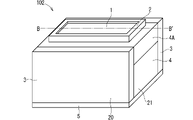
- FIG. 1 is a perspective view showing the configuration of a semiconductor device 101 according to Embodiment 1.
- FIG. FIG. 2 is a cross-sectional view taken along line A-A' shown in FIG.
- Semiconductor device 101 includes semiconductor substrate 31 , transistor region 6 , trench gate 15 , termination region 7 , front surface electrode 1 , peripheral insulating layer 2 , rear surface electrode 5 , first amorphous layer 3 and second amorphous layer 4 . include.
- the semiconductor substrate 31 is made of, for example, a semiconductor such as Si, or a so-called wide bandgap semiconductor such as SiC, GaN, or gallium oxide. Moreover, the semiconductor substrate 31 has a rectangular shape in plan view. The semiconductor substrate 31 has two first side surfaces 20 facing each other and two second side surfaces 21 facing each other. Its first side 20 is not parallel to the second side 21 .
- a transistor region 6 corresponds to a region in which a transistor is formed in the semiconductor substrate 31 .
- the semiconductor substrate 31 includes transistors.
- the trench gate 15 is provided on the upper surface of the semiconductor substrate 31 .
- the trench gate 15 forms part of the transistor.
- one transistor cell corresponds to a region divided by trench gates 15 .
- Trench gate 15 extends in one direction on the upper surface of semiconductor substrate 31 .
- the trench gate 15 extends in the depth direction in FIG. 2, in other words, in the horizontal direction in FIG.
- first side surface 20 of semiconductor substrate 31 is parallel to the extending direction of trench gate 15 .
- a second side surface 21 of the semiconductor substrate 31 is orthogonal to the extending direction of the trench gate 15 .
- the termination region 7 is provided so as to surround the transistor region 6 .
- a breakdown voltage holding structure 7A is provided in the termination region 7 .
- the breakdown voltage holding structure 7A holds the breakdown voltage of the transistor.
- Various structures are appropriately selected for the breakdown voltage holding structure 7A.
- the breakdown voltage holding structure 7A is, for example, an FLR (Field Limiting Ring), a VLD (Variation of Lateral Doping), or the like formed on the surface layer on the upper surface side of the semiconductor substrate 31 .
- the first amorphous layer 3 is formed on the first side surface 20 of the semiconductor substrate 31 .
- the second amorphous layer 4 is formed on the second side surface 21 of the semiconductor substrate 31 .
- the thickness of the first amorphous layer 3 is different from the thickness of the second amorphous layer 4 .
- the thickness of the first amorphous layer 3 corresponds to the dimension in the direction from the first side surface 20 toward the inside of the semiconductor substrate 31 .
- the thickness of the second amorphous layer 4 corresponds to the dimension in the direction from the second side surface 21 toward the inside of the semiconductor substrate 31 .
- the first amorphous layer 3 may be formed on a part of the first side surface 20 or may be formed on the entire surface.
- the second amorphous layer 4 may be formed on a part of the second side surface 21 or may be formed on the entire surface.
- the first amorphous layer 3 and the second amorphous layer 4 contain the same elements as the elements forming the crystals of the semiconductor substrate 31 .
- semiconductor substrate 31 is made of single crystal SiC except for portions of first amorphous layer 3 and second amorphous layer 4 .
- the first amorphous layer 3 and the second amorphous layer 4 are made of amorphous SiC.
- the surface electrode 1 is provided on the upper surface of the semiconductor substrate 31 .
- a surface electrode 1 is electrically connected to a transistor.
- the surface electrode 1 corresponds to the source electrode 17 of the transistor.
- the outer peripheral insulating layer 2 covers the outer periphery of the surface electrode 1 .
- the outer peripheral insulating layer 2 insulates the surface electrode 1 from the outer peripheral portion of the semiconductor substrate 31 .
- the back electrode 5 is provided on the bottom surface of the semiconductor substrate 31 .
- the back electrode 5 is electrically connected to the transistor.
- the back electrode 5 corresponds to the drain electrode 18 of the transistor.
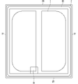
- FIG. 3 is a diagram showing the detailed configuration of the upper surface of the semiconductor device 101.
- FIG. A surface electrode 1 , an interlayer insulating film 16 , a gate connecting portion 19 and an outer peripheral insulating layer 2 are provided on the upper surface of the semiconductor device 101 .
- the gate connection portion 19 is electrically connected to the gate electrode (not shown) of the transistor.
- the outer insulating layer 2 partially covers the surface electrode 1 , the gate connecting portion 19 and the interlayer insulating film 16 .
- Peripheral insulating layer 2 has an opening through which part of surface electrode 1 and gate connecting portion 19 are exposed.
- FIG. 4 is a cross-sectional view showing the structure of the transistor region 6 according to the first embodiment.
- Semiconductor device 101 includes, in transistor region 6, n-type source layer 11, p-type base layer 10, p-type bottom base layer 12, n-type drift layer 9, n-type SiC layer 8, trench gate 15, interlayer insulating film 16, It includes a source electrode 17 and a drain electrode 18 .
- Semiconductor substrate 31 corresponds to the range from the upper surface of n-type source layer 11 or p-type base layer 10 to the lower surface of n-type SiC layer 8 .
- N-type source layer 11, p-type base layer 10, p-type bottom base layer 12 and n-type drift layer 9 are made of single crystal SiC.
- the n-type SiC layer 8 originates, for example, from the structure of the n-type SiC wafer before each structure is formed.
- the source electrode 17 corresponds to the surface electrode 1 in FIGS. 1-3.
- Drain electrode 18 corresponds to rear electrode 5 in FIGS.
- the trench gate 15 includes a gate insulating film 13 and a gate electrode 14 .
- the gate insulating film 13 is formed along the inner walls of trenches formed in the depth direction from the upper surface of the semiconductor substrate 31 .
- a gate electrode 14 is formed inside the trench with the gate insulating film 13 interposed therebetween.
- the interlayer insulating film 16 is provided on the gate electrode 14 . Since the source electrode 17 covers the interlayer insulating film 16 , it can be said that the interlayer insulating film 16 is provided between the lower surface of the source electrode 17 and the upper surface of the semiconductor substrate 31 . As shown in FIG. 2, the interlayer insulating film 16 covers the breakdown voltage holding structure 7A of the termination region 7 in the outer peripheral portion of the semiconductor substrate 31. As shown in FIG.
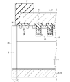
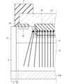
- FIG. 5 is a cross-sectional view showing the configuration of the end portion of the semiconductor device 101.
- FIG. 6 is an enlarged cross-sectional view of the configuration of the end portion of the semiconductor device 101.
- the thickness ty of the first amorphous layer 3 corresponds to the dimension in the direction from the first side surface 20 toward the inside of the semiconductor substrate 31 .
- the thickness of the second amorphous layer 4 similarly corresponds to the dimension in the direction from the second side surface 21 toward the inside of the semiconductor substrate 31 .
- FIG. 7 is a diagram showing an example of a transmission electron microscopy (TEM) image of the first amorphous layer 3 in Embodiment 1.
- TEM transmission electron microscopy
- FIG. 7 the contrast is more homogeneous in the area on the right than in the area on the left.
- the left region corresponds to the first amorphous layer 3 and the right region corresponds to the single crystal layer.
- the thickness of the area on the left side (horizontal dimension in the figure) is measured as the thickness of the first amorphous layer 3 .
- the TEM image of the second amorphous layer 4 is the same as the TEM image shown in FIG. Therefore, the thickness of the second amorphous layer 4 is also measured in the same manner as the thickness of the first amorphous layer 3 .
- the first amorphous layer 3 and the second amorphous layer 4 are formed outside the interlayer insulating film 16 covering the termination region 7 in plan view. Moreover, it is preferable that the first amorphous layer 3 and the second amorphous layer 4 are separated from the outer edge of the interlayer insulating film 16 by 3 ⁇ m or more.
- a distance dy between the first amorphous layer 3 and the outer edge of the interlayer insulating film 16 is defined as shown in FIGS.
- the distance dy corresponds to the distance from the interface between the first amorphous layer 3 and the single-crystal layer to the perpendicular extending downward from the outer edge of the interlayer insulating film 16 .
- the distance between the second amorphous layer 4 and the outer edge of the interlayer insulating film 16 is similarly defined.
- FIG. 8 is a flow chart showing the manufacturing process of the semiconductor device 101 according to the first embodiment.
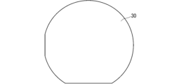
- FIG. 9 is a plan view showing the configuration of the n-type SiC wafer 30.
- FIG. 10 is a plan view showing a state in which a semiconductor device 101 is formed on the n-type SiC wafer 30.
- the semiconductor devices 101 shown in FIGS. 1 and 2 are obtained by dividing the plurality of semiconductor devices individually by dicing or the like.
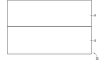
- step S1 an n-type SiC wafer 30 is prepared and an n-type drift layer 9 is formed.
- 11A and 11B are diagrams showing a step of forming the n-type drift layer 9 on the upper surface of the n-type SiC layer 8.
- the n-type SiC layer 8 is the n-type SiC wafer 30 itself.
- N-type drift layer 9 is formed by epitaxial growth.
- step S2 the p-type base layer 10 is formed.
- 12A and 12B are diagrams showing a step of forming the p-type base layer 10.
- FIG. A p-type impurity is ion-implanted through a mask having an opening in a predetermined region on the upper surface of n-type drift layer 9 .
- the mask is made of resist or the like.
- a p-type impurity is, for example, boron (B) or aluminum (Al).
- the p-type base layer 10 is formed on the entire surface of the n-type drift layer 9. As shown in FIG.
- step S3 the n-type source layer 11 is formed.
- 13A and 13B are diagrams showing a step of forming the n-type source layer 11.
- FIG. An n-type impurity is ion-implanted through a mask having an opening in a predetermined region on the upper surface of the p-type base layer.
- the mask is made of resist or the like.
- the n-type impurity is phosphorus (P) or nitrogen (N), for example.
- the SiC wafer 30 is heat-treated at a high temperature. The heat treatment electrically activates the p-type impurity implanted into p-type base layer 10 and the n-type impurity implanted into n-type source layer 11 .
- FIG. 14 is a diagram showing a step of forming trenches.
- a mask having openings in predetermined regions on the upper surfaces of p-type base layer 10 and n-type source layer 11 is formed.
- the mask is made of, for example, resist.
- a trench is formed by dry etching using plasma or the like.
- the mask may be a TEOS-based oxide, in which case the deeper trenches are formed.
- a p-type bottom base layer 12 is formed at the bottom of the trench.
- 15A and 15B are diagrams showing a step of forming the p-type bottom base layer 12.
- the p-type bottom base layer 12 is formed by ion-implanting p-type impurities.
- a p-type impurity is, for example, boron (B) or aluminum (Al).
- the p-type bottom base layer 12 reduces electric field concentration at the bottom of the trench.
- FIG. 16 is a diagram showing a step of forming the gate insulating film 13.
- the gate insulating film 13 is formed by thermal oxidation in order to remove plasma damage during formation of the trench gate 15 .
- gate insulating film 13 is formed by oxidizing n-type drift layer 9 on the inner wall of the trench.
- the thickness of the gate oxide film is 20 nm or more and 80 nm or less, more preferably 30 nm or more and 70 nm or less.
- the thickness of the gate insulating film 13 on the sides of the trench is equal to or greater than the thickness of the gate insulating film 13 on the bottom of the trench.
- the thickness of the gate insulating film 13 on the side surfaces of the trench is preferably 10% or more thicker than the thickness of the gate insulating film 13 on the bottom of the trench.
- the gate insulating film 13 may be formed by a CVD (chemical vapor deposition) method.
- the gate electrode 14 is formed.
- 17A and 17B are diagrams showing a step of forming the gate electrode 14.
- FIG. 18A and 18B are diagrams showing a step of removing the surplus portion of the gate electrode 14.
- the gate electrode 14 is made of polysilicon, for example.
- the etching is preferably isotropic etching.
- the etching is, for example, dry etching using plasma containing SF6 , or wet etching using mixed acid containing hydrofluoric acid and nitric acid.
- an oxide layer 14A is formed on the surface of the gate electrode 14 by thermal oxidation.
- the oxidation temperature is 850° C. or higher and 1050° C. or lower, more preferably 900° C. or higher and 1000° C. or lower.
- the thickness of the oxide layer 14A is 10 nm or more and 40 nm or less, more preferably 20 nm or more and 35 nm or less.
- FIG. 20 is a diagram showing a step of forming an interlayer insulating film 16.
- the interlayer insulating film 16 is deposited using the CVD method, and patterned by photolithography and etching after the deposition. Impurities such as B (boron) and P (phosphorus) may be introduced into the interlayer insulating film 16 . By introducing the impurity, the corners of the interlayer insulating film 16 are rounded.
- the interlayer insulating film 16 is made of, for example, silicon nitride (Si x N y ) or silicon oxide (SiO 2 ).
- the thickness of interlayer insulating film 16 is preferably 0.5 ⁇ m or more and 2.0 ⁇ m or less.
- the source electrode 17 is formed.
- 21A and 21B are diagrams showing a step of forming the source electrode 17.
- the source electrode 17 is made of aluminum, nickel, an aluminum alloy, or the like. Aluminum alloys contain aluminum and silicon.
- a barrier metal may be inserted between source electrode 17 and p-type base layer 10 and between source electrode 17 and n-type source layer 11 .
- the barrier metal is formed of titanium or a titanium compound such as titanium nitride (TiN).
- the outer insulating layer 2 is formed as shown in FIG.
- the outer peripheral insulating layer 2 is made of, for example, polyimide resin or silicone resin.
- the peripheral insulating layer 2 is preferably formed using a photolithographic technique in order to form a desired shape with high precision. Furthermore, an etching technique may be used together.
- the method for forming the outer peripheral insulating layer 2 is not limited to them, and a screen printing technique or a drawing application technique may be used.
- step S9 the SiC wafer 30 is thinned, that is, the n-type SiC layer 8 is thinned.
- FIG. 22 is a diagram showing a step of thinning the n-type SiC layer 8. As shown in FIG. The lower surface of the SiC wafer 30, that is, the lower surface of the n-type SiC layer 8 is ground by machining with a grindstone.
- the drain electrode 18 is formed.
- 23A and 23B are diagrams showing a step of forming the drain electrode 18.
- the drain electrode 18 is formed by sputtering, for example.
- the drain electrode 18 is, for example, a nickel film.
- the thickness of the drain electrode 18 is, for example, about 600 nm.
- the drain electrode 18 may be a laminated film of a nickel film and a metal film having poor reactivity with the outside.
- the laminated film prevents the nickel surface from being oxidized.
- Metals with poor reactivity with the outside include gold and silver. The wettability between the nickel film and the solder alloy is improved, and a good bonding state is obtained.
- a plurality of semiconductor devices are formed on one SiC wafer 30 through steps S1 to S10 described above.
- the plurality of semiconductor devices are divided into individual semiconductor devices 101 in steps S11 and S12 below.
- the first amorphous layer 3 and the second amorphous layer 4 are formed.
- step S11 the first amorphous layer 3 is formed.
- 24A and 24B are diagrams showing a step of forming the first amorphous layer 3.
- FIG. A plurality of semiconductor devices formed on the SiC wafer 30 are divided into individual semiconductor devices 101 by dicing.
- the first amorphous layer 3 is formed when the SiC wafer 30 is diced along the longitudinal direction of the trench gates 15 . More specifically, blade 32 used for dicing cuts drain electrode 18 , n-type SiC layer 8 and n-type drift layer 9 .
- the first amorphous layer 3 is formed by friction between the blade 32 and each semiconductor layer. In other words, when the blade 32 rubs each semiconductor layer, the single crystal forming each semiconductor layer is altered.
- compressive stress or tensile stress is generated between the single crystal and the abrasive grains contained in the blade 32 during dicing.
- the heat generated by the stress transforms the single crystal into an amorphous state.
- the contact portions between the blade 32 and each semiconductor layer generate heat, so that the first amorphous layer 3 is formed on the first side surface 20 of the semiconductor substrate 31 .
- the blade 32 is, for example, an electroformed blade, but is not limited thereto.
- a blade having a desired abrasive grain size can be appropriately selected.
- the blade rotation speed is between 10,000 rpm and 30,000 rpm.
- the blade feed speed is 5 mm/sec or more and 100 mm/sec or less. These blade rotation speed and feed speed are appropriately adjusted according to the blade material and the dicing device. In Embodiment 1, the blade rotation speed is 20,000 rpm and the blade feed speed is 20 mm/sec.
- step S12 the second amorphous layer 4 is formed.
- the second amorphous layer 4 is formed when the SiC wafer 30 is diced along the lateral direction of the trench gate 15 .
- the dicing conditions in step S12 are different from the dicing conditions in step S11. Therefore, the thickness of the second amorphous layer 4 is different from the thickness of the first amorphous layer 3 .
- the larger the abrasive grain size contained in the blade 32 the thicker the amorphous layer.
- the smaller the abrasive grain size contained in the blade 32 the thinner the amorphous layer.
- Amorphous layers are formed on the four side surfaces of the semiconductor substrate 31 by the above steps S11 and S12.
- FIG. 25 is a diagram showing the relationship between the distance between the amorphous layer and the interlayer insulating film 16 and the source-drain leakage current.
- the gate voltage is -15V.
- a voltage of 1200 V is applied between the source and the drain as a rated voltage.
- the distance dx indicates the distance between the second amorphous layer 4 and the interlayer insulating film 16
- the distance dy indicates the distance between the first amorphous layer 3 and the interlayer insulating film 16. ing.
- the leakage current between the source and the drain is reduced when the distance between the amorphous layer and the interlayer insulating film 16 is 3 ⁇ m or more.
- the gate voltage at which the transistor is turned off is not limited to -15V.
- the gate voltage is set arbitrarily, such as -5V or 0V.
- the voltage applied between the source and the drain is not limited to 1200V.
- the impurity concentration of the n-type drift layer 9 is appropriately designed, similar results can be obtained by applying a voltage in the range of 600V to 6500V between the source and the drain. That is, when the distance between the amorphous layer and the interlayer insulating film 16 is 3 ⁇ m or more, the leakage current between the source and the drain is reduced.
- FIG. 26 is a diagram showing a state in which the semiconductor device 101 is mounted on leads.
- Back electrode 5 (not shown in FIG. 26) of semiconductor device 101 is connected to first lead 22 via solder 23 .
- Surface electrode 1 (not shown in FIG. 26) of semiconductor device 101 is connected to second lead 24 by wire 25 .
- the first lead 22 and the second lead 24 have a plate shape and are made of metal.
- the gate connection 19 is similarly connected to appropriate leads by wires.
- a switching test of 10,000 cycles was performed in an environment of 150° C. on the semiconductor device 101 mounted in this way.
- FIG. 27 is a diagram showing the relationship between the thickness ty of the first amorphous layer 3 and the chip failure probability.
- FIG. 27 was performed on five types of semiconductor devices 101 having a ratio of the thickness t y of the first amorphous layer 3 to the thickness t x of the second amorphous layer 4 from 0.9 to 1.3. This is the result of a switching test.
- the chip failure probability is normalized by the value when the thickness t y of the first amorphous layer 3 is 0.02 ⁇ m and the thickness ratio t x /t y of the two amorphous layers is 1.0. It is When the thickness t y of the first amorphous layer 3 is 0.05 ⁇ m or more and the thickness ratio t x /t y of the two amorphous layers is 1.1 or less, the chip failure probability after switching is greatly reduced.
- FIG. 28 is a bird's-eye view schematically showing the internal configuration of the semiconductor device 101 according to the first embodiment.
- FIG. 29 is a diagram showing the configuration of the semiconductor device 101 in a cross section perpendicular to the extending direction of the trench gate 15. As shown in FIG. FIG. 29 corresponds to a cross section of the end portion of the semiconductor device 101 when FIG. 28 is viewed from the front.
- FIG. 29 shows the thickness ty of first amorphous layer 3 and the distance dy between first amorphous layer 3 and interlayer insulating film 16 .
- arrows schematically show the flow of current when the semiconductor device 101 is in the ON state. Since a channel is formed near the trench gate 15, the current path does not spread.
- FIG. 30 is a diagram showing the configuration of the semiconductor device 101 in a cross section parallel to the extending direction of the trench gate 15. As shown in FIG. FIG. 30 corresponds to a cross section of the end portion of the semiconductor device 101 when FIG. 28 is viewed from the right side. FIG. 30 shows the thickness t x of the second amorphous layer 4 and the distance d x between the second amorphous layer 4 and the interlayer insulating film 16 . Furthermore, in FIG. 30, arrows schematically indicate the flow of current when the semiconductor device 101 is in the ON state. A channel is formed in the vicinity of the trench gate 15, but the current spreads at the end of the trench gate 15 to flow. That is, the peripheral portion of the trench gate 15 also becomes part of the current path.
- the thickness t x of the second amorphous layer 4 with respect to the thickness t y of the first amorphous layer 3 is 1.1 or less, the current flowing through the amorphous layer, which has a higher electrical resistance than the single crystal, is reduced and chip failure is prevented.
- the semiconductor device 101 includes the semiconductor substrate 31 , the trench gate 15 , the first amorphous layer 3 and the second amorphous layer 4 .
- Semiconductor substrate 31 includes at least one semiconductor element of a transistor and a diode.
- Trench gate 15 includes an electrode that controls the state of the semiconductor device. Trench gate 15 is provided on the upper surface of semiconductor substrate 31 .
- the first amorphous layer 3 is formed on the first side surface 20 of the semiconductor substrate 31 .
- the second amorphous layer 4 is formed on the second side surface 21 of the semiconductor substrate 31 .
- the first angle between the first side surface 20 and the extending direction of the trench gate 15 is smaller than the second angle between the second side surface 21 and the extending direction of the trench gate 15, or the first side surface 20 is It is parallel to the extending direction of the trench gate 15 .
- the thickness of the first amorphous layer 3 in the direction from the first side surface 20 toward the inside of the semiconductor substrate 31 is different from the thickness of the second amorphous layer 4 in the direction from the second side surface 21 toward the inside of the semiconductor substrate 31. different.
- Such a semiconductor device 101 reduces current concentration to the outer periphery of the semiconductor device 101 during switching operation. Therefore, reliability of the semiconductor device 101 is improved.
- the semiconductor device 101 is, for example, a semiconductor device for power control (so-called power semiconductor device).
- Semiconductor device 101 controls current flowing between front electrode 1 and back electrode 5 .
- a semiconductor element included in the semiconductor device 101 is not limited to a MOSFET (Metal Oxide Semiconductor Field Effect Transistor).
- the semiconductor element may be any semiconductor element including the trench gate 15, such as an IGBT (Insulated Gate Bipolar Transistor), a Schottky barrier diode, or the like.
- the semiconductor device 101 may be an RC-IGBT (Reverse-Conducting IGBT) in which an IGBT and a freewheeling diode are formed in one semiconductor substrate 31 .
- the first side surface 20 and the second side surface 21 are defined by the direction in which the trench gate 15 extends.
- the trench gate 15 is not limited to the trench gate 15 constituting the MOSFET. That is, the trench gate 15 that defines the first side surface 20 and the second side surface 21 may be a trench gate that constitutes a semiconductor element such as an IGBT or a freewheeling diode.
- the semiconductor substrate 31 is preferably made of a wide bandgap semiconductor.
- SiC is superior to Si in withstand voltage and heat resistance, it enables the semiconductor device 101 to have high withstand voltage, low loss, and use in a high temperature environment.
- a semiconductor device 101 made of SiC is suitable for components constituting an inverter.
- the first side surface 20 of the semiconductor substrate 31 need not be parallel to the extending direction of the trench gate 15 .
- the second side surface 21 of the semiconductor substrate 31 need not be perpendicular to the extending direction of the trench gate 15 .
- the first angle formed by the first side surface 20 and the extending direction of the trench gate 15 should be smaller than the second angle formed by the second side surface 21 and the extending direction of the trench gate 15 .
- the crystal plane on the first side surface 20 of the semiconductor device 101 is not equivalent to the crystal plane on the second side surface 21 .
- the second side surface 21 is diced under the same dicing conditions as the first side surface 20, the first amorphous layer 3 and the second amorphous layer 4 having different thicknesses are formed. is self-formed. That is, if the semiconductor substrate 31 is made of a hexagonal material such as SiC, the dicing conditions in step S12 do not necessarily have to be different from the dicing conditions in step S11.
- trench gates 15 Although five trench gates 15 are shown in FIGS. 2 and 4, the number of trench gates 15 is not limited thereto. An arbitrary number of trench gates 15 may be arranged discretely in the horizontal direction of FIG.
- Embodiment 2 ⁇ Embodiment 2>
- the same reference numerals are given to the same components as in Embodiment 1, and detailed description thereof will be omitted.
- FIG. 31 is a perspective view showing the configuration of the semiconductor device 102 according to the second embodiment.
- 32 is a cross-sectional view taken along line B-B' shown in FIG. 31.
- the semiconductor device 102 includes a semiconductor substrate 31, a transistor region 6, a trench gate 15, a termination region 7, a front surface electrode 1, a peripheral insulating layer 2, a rear surface electrode 5, a first amorphous layer 3, a second amorphous layer 4 and It includes a single crystal layer 4A.
- Semiconductor device 102 of the second embodiment differs from semiconductor device 101 of the first embodiment in that it includes single crystal layer 4A.
- the second amorphous layer 4 is formed below the second side surface 21 . Specifically, the second amorphous layer 4 is formed on the lower portion of the side surface of the n-type drift layer 9 and the side surface of the n-type SiC layer 8 . In other words, the second amorphous layer 4 does not reach the upper surface of the semiconductor substrate 31 on the second side surface 21 .
- the single crystal layer 4A is formed on the upper part of the second side surface 21. Specifically, the single crystal layer 4A is formed on the side surface of the n-type drift layer 9 . In other words, the single crystal layer 4A is provided above the second amorphous layer 4 .
- the single crystal layer 4A is made of SiC forming the n-type drift layer 9 .
- the single crystal layer 4A is not provided below the interface between the second amorphous layer 4 and the single crystal layer 4A. Only the second amorphous layer 4 is provided below the interface between the second amorphous layer 4 and the single crystal layer 4A. On the second side surface 21, the second amorphous layer 4 is not provided above the interface between the second amorphous layer 4 and the single crystal layer 4A. Only the single crystal layer 4A is provided above the interface between the second amorphous layer 4 and the single crystal layer 4A.
- Steps S1 to S11 are the same as the respective steps in the first embodiment.
- a laser beam is irradiated along the dicing line extending in the lateral direction of the trench gate 15.
- Laser light has a wavelength in the near-ultraviolet region to the visible light region. For example, its wavelength is 380 nm.
- the laser light is focused on the lower portion of the n-type drift layer 9 and the n-type SiC layer 8 .
- the laser light transforms the single crystal into an amorphous state, forming the second amorphous layer 4 .
- laser light is applied three times and the processing speed is 500 mm/sec.
- the thickness of the semiconductor substrate 31 to be processed is approximately 100 ⁇ m.
- the SiC wafer 30 is divided with the second amorphous layer 4 as a starting point by applying stress to the SiC wafer 30 .
- a plurality of semiconductor devices formed on one SiC wafer 30 are divided into individual semiconductor devices 102 .
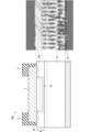
- FIG. 33 is a diagram showing the correspondence relationship between the second side surface 21 of the semiconductor device 102 schematically shown and the optical microscope image of the second side surface 21 .
- the second amorphous layer 4 is formed below the second side surface 21 and the single crystal layer 4A is formed above the second side surface 21 .
- FIG. 33 also shows the width w of the single crystal layer 4A.
- FIG. 34 is a schematic diagram showing the state of a three-point bending test of the semiconductor device 102 according to the second embodiment.
- the longitudinal direction of trench gate 15 corresponds to the horizontal direction in FIG.
- the distance between the fulcrums is 8 mm.
- the upper indenter descends toward the semiconductor device 102 at a speed of 0.5 mm/min.
- the bending strength was calculated based on the amount of deflection and the breaking load at that time.
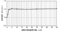
- FIG. 35 is a diagram showing the relationship between the width w of the single crystal layer 4A on the second side surface 21 and the bending strength of the semiconductor device 102. As shown in FIG. The bending strength is standardized by the value when the width w of the single crystal layer 4A is 0 ⁇ m. When the width w of the single crystal layer 4A is 2 ⁇ m or more, the mechanical strength of the semiconductor device 102 is improved.
- the chip failure probability in Embodiment 2 is the same as the result shown in FIG.
- the path of current flowing from the back surface to the front surface of semiconductor device 102 does not extend to the outer peripheral portion of semiconductor device 102, as in FIGS. Therefore, the single crystal layer 4A formed on the second side surface 21 does not induce chip failure.
- the semiconductor device 102 according to the second embodiment increases the chip strength while preventing breakage due to the switching operation. That is, not only reliability is improved, but also the mechanical strength of the semiconductor device 102 is increased.
- the second amorphous layer 4 is formed by laser.
- the stress received from the blade 32 causes the plurality of semiconductor devices to form the second amorphous layer. Chipping occurs starting from layer 4 . Therefore, it is preferable to form the second amorphous layer 4 with a laser after forming the first amorphous layer 3 with the blade 32 .
- trench gate 15 Although one continuous trench gate 15 is shown in FIG. 32, the configuration of the trench gate 15 is not limited to this. Two trench gates separated at the center of the transistor region 6 may be arranged. A plurality of trench gates divided into an arbitrary number may be discretely arranged in the horizontal direction of FIG.
- Embodiment 3 In Embodiment 3, constituent elements similar to Embodiments 1 and 2 are denoted by the same reference numerals, and detailed description thereof will be omitted.
- FIG. 36 is a perspective view showing the configuration of the semiconductor device 103 according to the third embodiment.
- 37 is a cross-sectional view taken along line C-C' shown in FIG. 36.
- the semiconductor device 103 includes a semiconductor substrate 31, a transistor region 6, a trench gate 15, a termination region 7, a surface electrode 1, a peripheral insulating layer 2, a back surface electrode 5, a lower first amorphous layer 3L, and an upper first amorphous layer. 3U, lower second amorphous layer 4L and upper second amorphous layer 4U.
- first amorphous layer 3 is composed of lower first amorphous layer 3L and upper first amorphous layer 3U
- second amorphous layer 4 is composed of lower second amorphous layer 3L and upper first amorphous layer 3U.
- the semiconductor device 101 of the first embodiment differs from the semiconductor device 101 of the first embodiment in that it consists of a crystalline layer 4L and an upper second amorphous layer 4U.
- the thicknesses of the first amorphous layer 3 and the second amorphous layer 4 on the side surfaces of the semiconductor device 103 differ between the upper portion and the lower portion of the semiconductor device 103 .
- the upper first amorphous layer 3U is formed above the first amorphous layer 3 on the first side surface 20. Specifically, the upper first amorphous layer 3U is formed on the side surface of the n-type drift layer 9 .
- the lower first amorphous layer 3L is formed on the side surfaces of the n-type drift layer 9 and the n-type SiC layer 8, ie, the lower surface side of the semiconductor device 103, in a form connected to the upper first amorphous layer 3U. ing.
- the upper second amorphous layer 4U is formed above the second amorphous layer 4 on the second side surface 21. Specifically, the upper second amorphous layer 4U is formed on the side surface of the n-type drift layer 9 .
- the second amorphous layer 4 is formed on the side surfaces of the n-type drift layer 9 and the n-type SiC layer 8, that is, on the lower surface side of the semiconductor device 103, in a form connected to the upper second amorphous layer 4U.
- the boundary between the upper first amorphous layer 3U and the lower first amorphous layer 3L and the boundary between the upper second amorphous layer 4U and the lower second amorphous layer 4L are not necessarily of the same height.
- Steps S1 to S10 are the same as the respective steps in the first embodiment, but steps S11 and S12 are different from the first embodiment.
- step S11 the upper first amorphous layer 3U and the lower first amorphous layer 3L are formed.
- FIG. 38 shows a step of forming the upper first amorphous layer 3U.
- a plurality of semiconductor devices formed on the SiC wafer 30 are divided into individual semiconductor devices 103 by dicing.
- Upper first amorphous layer 3U is formed when SiC wafer 30 is diced along the longitudinal direction of trench gate 15 . More specifically, blade 32 used for dicing cuts at least part of n-type drift layer 9 . At that time, the friction between the blade 32 and the n-type drift layer 9 forms the upper first amorphous layer 3U.
- the lower first amorphous layer 3L is formed on the remaining portion of the n-type drift layer 9 and the n-type SiC layer 8, and the drain electrode 18 is cut.
- the blade 32 is, for example, an electroformed blade, but is not limited thereto.
- a blade having a desired abrasive grain size can be appropriately selected.
- the blade rotation speed is between 10,000 rpm and 30,000 rpm.
- the blade feed speed is 5 mm/sec or more and 100 mm/sec or less. These blade rotation speed and feed speed are appropriately adjusted according to the blade material and the dicing device. In Embodiment 3, the blade rotation speed is 20,000 rpm and the blade feed speed is 20 mm/sec.
- step S12 the upper second amorphous layer 4U and the lower second amorphous layer 4L are formed.
- Upper second amorphous layer 4U and lower second amorphous layer 4L are formed when SiC wafer 30 is diced along the lateral direction of trench gate 15 .
- the dicing conditions in step S12 are different from the dicing conditions in step S11. Therefore, the thickness of the second amorphous layer 4 is different from the thickness of the first amorphous layer 3 .
- the method of forming the upper second amorphous layer 4U and the lower second amorphous layer 4L is the same as the method of forming the upper first amorphous layer 3U and the first amorphous layer 3 described above.
- a three-point bending test of the semiconductor device 103 as shown in the schematic diagram of FIG. 34 was performed.
- the extending direction of the trench gate 15 corresponds to the horizontal direction in FIG.
- the distance between the fulcrums is 8 mm.
- the upper indenter descends toward the semiconductor device 103 at a speed of 0.5 mm/min.
- the bending strength was calculated based on the amount of deflection and the breaking load at that time.
- FIG. 39 is a diagram showing the configuration of the end portion of the semiconductor device 103 in a cross section orthogonal to the extending direction of the trench gate 15. As shown in FIG. In addition to the thickness ty of the lower first amorphous layer 3L and the distance d y between the lower first amorphous layer 3L and the interlayer insulating film 16, FIG. A difference d in thickness between the amorphous layer 3U and the lower first amorphous layer 3L is shown. Furthermore, in FIG. 39, arrows schematically indicate the flow of current when the semiconductor device 103 is in the ON state. Since a channel is formed near the trench gate 15, the current path does not spread.
- FIG. 40 is a diagram showing the relationship between the thickness difference d between the upper first amorphous layer 3U and the lower first amorphous layer 3L on the first side surface 20 and the bending strength of the semiconductor device 103.
- the bending strength is standardized by the value when the thickness difference d is 0 ⁇ m. When the thickness difference d is 0.5 ⁇ m or more, the mechanical strength of the semiconductor device 103 is improved.
- FIG. 40 shows an examination of the difference d in thickness between the upper first amorphous layer 3U and the lower first amorphous layer 3L on the first side surface 20 and the bending strength of the semiconductor device 103. Similar results were obtained for the relationship between the difference d in thickness between the upper second amorphous layer 4U and the lower second amorphous layer 4L in 21 and the bending strength of the semiconductor device 103 .
- the mechanical strength of the semiconductor device 102 is improved when the width w of the single crystal layer 4A is 2 ⁇ m or more. Also in Embodiment 3, it was confirmed that the mechanical strength of semiconductor device 103 was improved when upper first amorphous layer 3U had a width of 2 ⁇ m or more.
- FIG. 41 is a diagram showing the configuration of the semiconductor device 103 in a cross section parallel to the extending direction of the trench gate 15. As shown in FIG. FIG. 41 shows the thickness tx of the lower second amorphous layer 4L and the distance dx between the lower second amorphous layer 4L and the interlayer insulating film 16. As shown in FIG. Furthermore, in FIG. 41, arrows schematically show the flow of current when the semiconductor device 103 is in the ON state. A channel is formed in the vicinity of the trench gate 15, but the current spreads at the end of the trench gate 15 to flow. That is, the peripheral portion of the trench gate 15 also becomes part of the current path.
- the chip failure probability in Embodiment 3 is the same as the result shown in FIG.
- the path of current flowing from the back surface to the front surface of semiconductor device 103 does not extend to the outer peripheral portion of semiconductor device 103, as shown in FIGS. Therefore, the upper first amorphous layer 3U and the upper second amorphous layer 4U do not induce chip failure.
- the semiconductor device 103 according to the third embodiment increases the chip strength while preventing breakage due to the switching operation. In other words, not only is the reliability improved, but the mechanical strength of the semiconductor device 103 is increased.
- a top-side amorphous layer is provided on each of the first side surface 20 and the second side surface 21 of the semiconductor device 103 .
- the upper amorphous layer does not necessarily need to be provided on all side surfaces of the semiconductor device 103, and may be provided on only one side surface.
- Embodiment 4 In Embodiment 4, the same reference numerals are given to the same constituent elements as in Embodiments 1 to 3, and detailed description thereof will be omitted.
- FIG. 42 is a block diagram showing configurations of the power conversion device 200 and the power conversion system according to the fourth embodiment.
- the power conversion system includes a power supply 100, a power conversion device 200 and a load 300.
- the power supply 100 is a DC power supply.
- the power supply 100 supplies DC power to the power converter 200 .
- the power supply 100 is composed of, for example, a DC system, a solar battery, a storage battery, or the like.
- the power supply 100 may include a DC/DC converter that converts DC power output from the DC system into predetermined power.
- the power supply 100 may be configured with a rectifier circuit, an AC/DC converter, or the like connected to an AC system.
- the power converter 200 is a three-phase inverter connected between the power supply 100 and the load 300 .
- the power conversion device 200 converts the DC power supplied from the power supply 100 into AC power and supplies the AC power to the load 300 . A detailed configuration of the power converter 200 will be described later.
- the load 300 is driven by AC power supplied from the power converter 200 .
- a load 300 in the fourth embodiment is a three-phase electric motor.
- load 300 is not limited to a motor for a particular application.
- the load 300 may be an electric motor mounted on various electric devices.
- the electric motors are used, for example, in hybrid cars, electric cars, railroad cars, elevators, air conditioners, and the like.
- Power conversion device 200 includes main conversion circuit 201 , drive circuit 202 and control circuit 203 .
- the main conversion circuit 201 converts DC power into AC power and outputs it.
- Main conversion circuit 201 includes a switching element and a freewheeling diode (both not shown). By switching between the ON state and the OFF state of the switching element, the DC power supplied from power supply 100 is converted into AC power, and the AC power is supplied to load 300 .
- At least one of the switching element and freewheeling diode of main conversion circuit 201 is formed in semiconductor device 101 or 102 shown in the first or second embodiment.
- the semiconductor elements included in the semiconductor devices 101 and 102 described above correspond to the switching elements or freewheeling diodes of the main conversion circuit 201 .
- the main conversion circuit 201 in Embodiment 4 is a two-level three-phase full bridge circuit.
- the main conversion circuit 201 includes six switching elements and six free wheel diodes connected in parallel in opposite directions to the six switching elements.
- Main conversion circuit 201 includes an upper arm and a lower arm. One switching element belonging to the upper arm is connected in series to one switching element belonging to the lower arm. In other words, the six switching elements form upper and lower arms for every two switching elements connected in series.
- Each upper and lower arm constitutes each phase (U phase, V phase, W phase) of the full bridge circuit.
- Three-phase output terminals, that is, three output terminals of the main conversion circuit 201 are connected to the load 300 .
- the circuit configuration of the main conversion circuit 201 is an example, and is not limited to the above configuration.
- the drive circuit 202 generates drive signals for controlling the states of the switching elements of the main conversion circuit 201 .
- the drive circuit 202 outputs the drive signal to the control electrodes of the switching elements of the main conversion circuit 201 .
- a drive signal for turning on the switching element or a drive signal for turning off the switching element is output to the control electrode of each switching element.
- the driving signal is a voltage signal (ON signal) equal to or higher than the threshold voltage of the switching element.
- the drive signal is a voltage signal (OFF signal) below the threshold voltage of the switching element.
- the control electrode is gate electrode 14 .
- a control circuit 203 outputs a control signal for controlling the drive circuit 202 .
- the control signal is controlled such that predetermined power is supplied to load 300 .
- the control circuit 203 calculates the time during which the switching element of the main conversion circuit 201 should be in the ON state, that is, the ON time.
- the control circuit 203 outputs a control signal from the driving circuit 202 to the switching element so that an ON signal is output to the switching element at the timing when the switching element should be in the ON state, and an OFF signal is output to the switching element at the timing when the switching element is to be in the OFF state.
- the control circuit 203 performs PWM control that modulates the ON time according to the voltage to be output.
- the semiconductor devices 101 and 102 are applied to a two-level three-phase inverter. It is applied to various power converters. Semiconductor devices 101 and 102 are applicable to three-level or multi-level power converters. When power conversion device 200 supplies power to a single-phase load, semiconductor devices 101 and 102 may be applied to a single-phase inverter. When power conversion device 200 supplies power to a DC load or the like, semiconductor devices 101 and 102 may be applied to a DC/DC converter or an AC/DC converter.
- control target of the power converter 200 is not limited to the electric motor.
- the power conversion device 200 may control power conversion in, for example, an electric discharge machine, a laser processing machine, an induction heating cooker, a contactless power supply system, or the like.
- the power conversion device 200 may be applied to a power conditioner such as a photovoltaic power generation system, an electric storage system, or the like.
Landscapes
- Electrodes Of Semiconductors (AREA)
Priority Applications (4)
| Application Number | Priority Date | Filing Date | Title |
|---|---|---|---|
| CN202280062340.XA CN117941077A (zh) | 2021-09-22 | 2022-09-20 | 半导体装置以及电力转换装置 |
| JP2023549690A JPWO2023048122A1 (https=) | 2021-09-22 | 2022-09-20 | |
| DE112022004480.2T DE112022004480T5 (de) | 2021-09-22 | 2022-09-20 | Halbleitergerät und Leistungswandlungsgerät |
| US18/577,041 US20240321986A1 (en) | 2021-09-22 | 2022-09-20 | Semiconductor device and power converter |
Applications Claiming Priority (2)
| Application Number | Priority Date | Filing Date | Title |
|---|---|---|---|
| JP2021-154055 | 2021-09-22 | ||
| JP2021154055 | 2021-09-22 |
Publications (1)
| Publication Number | Publication Date |
|---|---|
| WO2023048122A1 true WO2023048122A1 (ja) | 2023-03-30 |
Family
ID=85719506
Family Applications (1)
| Application Number | Title | Priority Date | Filing Date |
|---|---|---|---|
| PCT/JP2022/034929 Ceased WO2023048122A1 (ja) | 2021-09-22 | 2022-09-20 | 半導体装置および電力変換装置 |
Country Status (5)
| Country | Link |
|---|---|
| US (1) | US20240321986A1 (https=) |
| JP (1) | JPWO2023048122A1 (https=) |
| CN (1) | CN117941077A (https=) |
| DE (1) | DE112022004480T5 (https=) |
| WO (1) | WO2023048122A1 (https=) |
Cited By (1)
| Publication number | Priority date | Publication date | Assignee | Title |
|---|---|---|---|---|
| EP4586766A3 (en) * | 2024-01-12 | 2025-11-05 | STMicroelectronics International N.V. | Method for forming a trench-gate metal-oxide-semiconductor field-effect transistor |
Citations (5)
| Publication number | Priority date | Publication date | Assignee | Title |
|---|---|---|---|---|
| JP2002050773A (ja) * | 2000-07-31 | 2002-02-15 | Shindengen Electric Mfg Co Ltd | 半導体装置 |
| JP2012064656A (ja) * | 2010-09-14 | 2012-03-29 | Mitsubishi Electric Corp | 半導体装置の製造方法 |
| WO2018190271A1 (ja) * | 2017-04-14 | 2018-10-18 | 三菱電機株式会社 | 炭化珪素半導体装置、電力変換装置、炭化珪素半導体装置の製造方法、および電力変換装置の製造方法 |
| JP2020027858A (ja) * | 2018-08-10 | 2020-02-20 | ローム株式会社 | SiC半導体装置 |
| JP2021077903A (ja) * | 2016-04-28 | 2021-05-20 | 株式会社タムラ製作所 | トレンチmos型ショットキーダイオード |
Family Cites Families (2)
| Publication number | Priority date | Publication date | Assignee | Title |
|---|---|---|---|---|
| JP7228040B2 (ja) | 2019-06-17 | 2023-02-22 | ローム株式会社 | SiC半導体装置およびその製造方法 |
| JP7129397B2 (ja) | 2019-12-06 | 2022-09-01 | ローム株式会社 | SiC半導体装置 |
-
2022
- 2022-09-20 WO PCT/JP2022/034929 patent/WO2023048122A1/ja not_active Ceased
- 2022-09-20 JP JP2023549690A patent/JPWO2023048122A1/ja not_active Ceased
- 2022-09-20 CN CN202280062340.XA patent/CN117941077A/zh not_active Withdrawn
- 2022-09-20 DE DE112022004480.2T patent/DE112022004480T5/de active Pending
- 2022-09-20 US US18/577,041 patent/US20240321986A1/en active Pending
Patent Citations (5)
| Publication number | Priority date | Publication date | Assignee | Title |
|---|---|---|---|---|
| JP2002050773A (ja) * | 2000-07-31 | 2002-02-15 | Shindengen Electric Mfg Co Ltd | 半導体装置 |
| JP2012064656A (ja) * | 2010-09-14 | 2012-03-29 | Mitsubishi Electric Corp | 半導体装置の製造方法 |
| JP2021077903A (ja) * | 2016-04-28 | 2021-05-20 | 株式会社タムラ製作所 | トレンチmos型ショットキーダイオード |
| WO2018190271A1 (ja) * | 2017-04-14 | 2018-10-18 | 三菱電機株式会社 | 炭化珪素半導体装置、電力変換装置、炭化珪素半導体装置の製造方法、および電力変換装置の製造方法 |
| JP2020027858A (ja) * | 2018-08-10 | 2020-02-20 | ローム株式会社 | SiC半導体装置 |
Cited By (1)
| Publication number | Priority date | Publication date | Assignee | Title |
|---|---|---|---|---|
| EP4586766A3 (en) * | 2024-01-12 | 2025-11-05 | STMicroelectronics International N.V. | Method for forming a trench-gate metal-oxide-semiconductor field-effect transistor |
Also Published As
| Publication number | Publication date |
|---|---|
| CN117941077A (zh) | 2024-04-26 |
| US20240321986A1 (en) | 2024-09-26 |
| JPWO2023048122A1 (https=) | 2023-03-30 |
| DE112022004480T5 (de) | 2024-07-18 |
Similar Documents
| Publication | Publication Date | Title |
|---|---|---|
| CN110473903B (zh) | 碳化硅半导体装置、电力变换装置以及碳化硅半导体装置的制造方法 | |
| JP6253854B1 (ja) | 半導体装置およびその製造方法、電力変換装置 | |
| US10026803B1 (en) | Semiconductor device, power conversion device, and method of manufacturing semiconductor device | |
| JP7846025B2 (ja) | 半導体基板の製造方法 | |
| JP6695498B2 (ja) | 炭化珪素半導体装置、電力変換装置、炭化珪素半導体装置の製造方法、および電力変換装置の製造方法 | |
| US10367090B2 (en) | Silicon carbide semiconductor device, power module, and power conversion device | |
| JP6947338B1 (ja) | 炭化珪素半導体装置および電力変換装置の製造方法 | |
| US20230290874A1 (en) | Method of manufacturing silicon carbide semiconductor device, silicon carbide semiconductor device, and power conversion apparatus | |
| WO2022168240A1 (ja) | 炭化珪素半導体装置および電力変換装置 | |
| JP7127748B2 (ja) | 炭化珪素半導体装置、電力変換装置および炭化珪素半導体装置の製造方法 | |
| WO2023048122A1 (ja) | 半導体装置および電力変換装置 | |
| JP6455514B2 (ja) | 半導体装置および半導体装置の製造方法 | |
| JP6584940B2 (ja) | 半導体装置の製造方法 | |
| JP6473073B2 (ja) | 半導体装置、パワーモジュール、電力変換装置、自動車および鉄道車両 | |
| JP7262672B2 (ja) | 半導体装置および電力変換装置 | |
| US20250113533A1 (en) | Semiconductor device and power conversion device | |
| US20250203924A1 (en) | Semiconductor device, method of manufacturing semiconductor device, and power conversion apparatus | |
| JP7529139B2 (ja) | 炭化珪素半導体装置とその製造方法、および、電力変換装置 | |
| WO2024214501A1 (ja) | 半導体装置及び電力変換装置 | |
| CN121003028A (zh) | 半导体装置以及电力转换装置 | |
| KR101822166B1 (ko) | 전력용 반도체의 제조방법 | |
| KR20160120871A (ko) | 전력용 반도체 장치 및 제조방법 | |
| KR20160120872A (ko) | 전력용 반도체 장치 및 제조방법 | |
| WO2025169440A1 (ja) | 炭化珪素半導体装置および電力変換装置 | |
| JP2024123834A (ja) | 炭化珪素半導体装置及び電力変換装置 |
Legal Events
| Date | Code | Title | Description |
|---|---|---|---|
| 121 | Ep: the epo has been informed by wipo that ep was designated in this application |
Ref document number: 22872876 Country of ref document: EP Kind code of ref document: A1 |
|
| WWE | Wipo information: entry into national phase |
Ref document number: 2023549690 Country of ref document: JP |
|
| WWE | Wipo information: entry into national phase |
Ref document number: 202280062340.X Country of ref document: CN |
|
| WWE | Wipo information: entry into national phase |
Ref document number: 112022004480 Country of ref document: DE |
|
| 122 | Ep: pct application non-entry in european phase |
Ref document number: 22872876 Country of ref document: EP Kind code of ref document: A1 |