WO2023047881A1 - 半導体装置およびその製造方法 - Google Patents
半導体装置およびその製造方法 Download PDFInfo
- Publication number
- WO2023047881A1 WO2023047881A1 PCT/JP2022/032094 JP2022032094W WO2023047881A1 WO 2023047881 A1 WO2023047881 A1 WO 2023047881A1 JP 2022032094 W JP2022032094 W JP 2022032094W WO 2023047881 A1 WO2023047881 A1 WO 2023047881A1
- Authority
- WO
- WIPO (PCT)
- Prior art keywords
- semiconductor element
- metal body
- terminal
- wiring
- surface metal
- Prior art date
- Legal status (The legal status is an assumption and is not a legal conclusion. Google has not performed a legal analysis and makes no representation as to the accuracy of the status listed.)
- Ceased
Links
Images













Classifications
-
- H—ELECTRICITY
- H10—SEMICONDUCTOR DEVICES; ELECTRIC SOLID-STATE DEVICES NOT OTHERWISE PROVIDED FOR
- H10W—GENERIC PACKAGES, INTERCONNECTIONS, CONNECTORS OR OTHER CONSTRUCTIONAL DETAILS OF DEVICES COVERED BY CLASS H10
- H10W72/00—Interconnections or connectors in packages
- H10W72/50—Bond wires
-
- H—ELECTRICITY
- H10—SEMICONDUCTOR DEVICES; ELECTRIC SOLID-STATE DEVICES NOT OTHERWISE PROVIDED FOR
- H10W—GENERIC PACKAGES, INTERCONNECTIONS, CONNECTORS OR OTHER CONSTRUCTIONAL DETAILS OF DEVICES COVERED BY CLASS H10
- H10W70/00—Package substrates; Interposers; Redistribution layers [RDL]
- H10W70/60—Insulating or insulated package substrates; Interposers; Redistribution layers
- H10W70/62—Insulating or insulated package substrates; Interposers; Redistribution layers characterised by their interconnections
- H10W70/65—Shapes or dispositions of interconnections
- H10W70/658—Shapes or dispositions of interconnections for devices provided for in groups H10D8/00 - H10D48/00
-
- H—ELECTRICITY
- H10—SEMICONDUCTOR DEVICES; ELECTRIC SOLID-STATE DEVICES NOT OTHERWISE PROVIDED FOR
- H10W—GENERIC PACKAGES, INTERCONNECTIONS, CONNECTORS OR OTHER CONSTRUCTIONAL DETAILS OF DEVICES COVERED BY CLASS H10
- H10W72/00—Interconnections or connectors in packages
-
- H—ELECTRICITY
- H10—SEMICONDUCTOR DEVICES; ELECTRIC SOLID-STATE DEVICES NOT OTHERWISE PROVIDED FOR
- H10W—GENERIC PACKAGES, INTERCONNECTIONS, CONNECTORS OR OTHER CONSTRUCTIONAL DETAILS OF DEVICES COVERED BY CLASS H10
- H10W72/00—Interconnections or connectors in packages
- H10W72/071—Connecting or disconnecting
- H10W72/073—Connecting or disconnecting of die-attach connectors
-
- H—ELECTRICITY
- H10—SEMICONDUCTOR DEVICES; ELECTRIC SOLID-STATE DEVICES NOT OTHERWISE PROVIDED FOR
- H10W—GENERIC PACKAGES, INTERCONNECTIONS, CONNECTORS OR OTHER CONSTRUCTIONAL DETAILS OF DEVICES COVERED BY CLASS H10
- H10W72/00—Interconnections or connectors in packages
- H10W72/071—Connecting or disconnecting
- H10W72/075—Connecting or disconnecting of bond wires
-
- H—ELECTRICITY
- H10—SEMICONDUCTOR DEVICES; ELECTRIC SOLID-STATE DEVICES NOT OTHERWISE PROVIDED FOR
- H10W—GENERIC PACKAGES, INTERCONNECTIONS, CONNECTORS OR OTHER CONSTRUCTIONAL DETAILS OF DEVICES COVERED BY CLASS H10
- H10W72/00—Interconnections or connectors in packages
- H10W72/30—Die-attach connectors
-
- H—ELECTRICITY
- H10—SEMICONDUCTOR DEVICES; ELECTRIC SOLID-STATE DEVICES NOT OTHERWISE PROVIDED FOR
- H10W—GENERIC PACKAGES, INTERCONNECTIONS, CONNECTORS OR OTHER CONSTRUCTIONAL DETAILS OF DEVICES COVERED BY CLASS H10
- H10W72/00—Interconnections or connectors in packages
- H10W72/851—Dispositions of multiple connectors or interconnections
-
- H—ELECTRICITY
- H10—SEMICONDUCTOR DEVICES; ELECTRIC SOLID-STATE DEVICES NOT OTHERWISE PROVIDED FOR
- H10W—GENERIC PACKAGES, INTERCONNECTIONS, CONNECTORS OR OTHER CONSTRUCTIONAL DETAILS OF DEVICES COVERED BY CLASS H10
- H10W74/00—Encapsulations, e.g. protective coatings
-
- H—ELECTRICITY
- H10—SEMICONDUCTOR DEVICES; ELECTRIC SOLID-STATE DEVICES NOT OTHERWISE PROVIDED FOR
- H10W—GENERIC PACKAGES, INTERCONNECTIONS, CONNECTORS OR OTHER CONSTRUCTIONAL DETAILS OF DEVICES COVERED BY CLASS H10
- H10W74/00—Encapsulations, e.g. protective coatings
- H10W74/40—Encapsulations, e.g. protective coatings characterised by their materials
-
- H—ELECTRICITY
- H10—SEMICONDUCTOR DEVICES; ELECTRIC SOLID-STATE DEVICES NOT OTHERWISE PROVIDED FOR
- H10W—GENERIC PACKAGES, INTERCONNECTIONS, CONNECTORS OR OTHER CONSTRUCTIONAL DETAILS OF DEVICES COVERED BY CLASS H10
- H10W90/00—Package configurations
-
- H—ELECTRICITY
- H10—SEMICONDUCTOR DEVICES; ELECTRIC SOLID-STATE DEVICES NOT OTHERWISE PROVIDED FOR
- H10W—GENERIC PACKAGES, INTERCONNECTIONS, CONNECTORS OR OTHER CONSTRUCTIONAL DETAILS OF DEVICES COVERED BY CLASS H10
- H10W90/00—Package configurations
- H10W90/701—Package configurations characterised by the relative positions of pads or connectors relative to package parts
-
- H—ELECTRICITY
- H10—SEMICONDUCTOR DEVICES; ELECTRIC SOLID-STATE DEVICES NOT OTHERWISE PROVIDED FOR
- H10W—GENERIC PACKAGES, INTERCONNECTIONS, CONNECTORS OR OTHER CONSTRUCTIONAL DETAILS OF DEVICES COVERED BY CLASS H10
- H10W99/00—Subject matter not provided for in other groups of this subclass
-
- H—ELECTRICITY
- H10—SEMICONDUCTOR DEVICES; ELECTRIC SOLID-STATE DEVICES NOT OTHERWISE PROVIDED FOR
- H10W—GENERIC PACKAGES, INTERCONNECTIONS, CONNECTORS OR OTHER CONSTRUCTIONAL DETAILS OF DEVICES COVERED BY CLASS H10
- H10W72/00—Interconnections or connectors in packages
- H10W72/851—Dispositions of multiple connectors or interconnections
- H10W72/874—On different surfaces
- H10W72/884—Die-attach connectors and bond wires
-
- H—ELECTRICITY
- H10—SEMICONDUCTOR DEVICES; ELECTRIC SOLID-STATE DEVICES NOT OTHERWISE PROVIDED FOR
- H10W—GENERIC PACKAGES, INTERCONNECTIONS, CONNECTORS OR OTHER CONSTRUCTIONAL DETAILS OF DEVICES COVERED BY CLASS H10
- H10W74/00—Encapsulations, e.g. protective coatings
- H10W74/10—Encapsulations, e.g. protective coatings characterised by their shape or disposition
-
- H—ELECTRICITY
- H10—SEMICONDUCTOR DEVICES; ELECTRIC SOLID-STATE DEVICES NOT OTHERWISE PROVIDED FOR
- H10W—GENERIC PACKAGES, INTERCONNECTIONS, CONNECTORS OR OTHER CONSTRUCTIONAL DETAILS OF DEVICES COVERED BY CLASS H10
- H10W90/00—Package configurations
- H10W90/701—Package configurations characterised by the relative positions of pads or connectors relative to package parts
- H10W90/731—Package configurations characterised by the relative positions of pads or connectors relative to package parts of die-attach connectors
- H10W90/734—Package configurations characterised by the relative positions of pads or connectors relative to package parts of die-attach connectors between a chip and a stacked insulating package substrate, interposer or RDL
-
- H—ELECTRICITY
- H10—SEMICONDUCTOR DEVICES; ELECTRIC SOLID-STATE DEVICES NOT OTHERWISE PROVIDED FOR
- H10W—GENERIC PACKAGES, INTERCONNECTIONS, CONNECTORS OR OTHER CONSTRUCTIONAL DETAILS OF DEVICES COVERED BY CLASS H10
- H10W90/00—Package configurations
- H10W90/701—Package configurations characterised by the relative positions of pads or connectors relative to package parts
- H10W90/751—Package configurations characterised by the relative positions of pads or connectors relative to package parts of bond wires
- H10W90/755—Package configurations characterised by the relative positions of pads or connectors relative to package parts of bond wires between a chip and a laterally-adjacent insulating package substrate, interpose or RDL
Definitions
- the disclosure in this specification relates to a semiconductor device and its manufacturing method.
- Patent Document 1 discloses a semiconductor device comprising a semiconductor chip having main electrodes on both sides, a first heat sink, a second heat sink, and signal terminals.
- a drain electrode is provided on one surface of the semiconductor chip, and a source electrode and a signal pad are provided on the back surface.
- a first heat sink is electrically connected to the drain electrode and a second heat sink is electrically connected to the source electrode.
- Signal terminals are connected to pads via bonding wires.
- One object of the disclosure is to provide a semiconductor device capable of reducing thermal resistance while reducing inductance, and a method of manufacturing the same.
- the semiconductor device disclosed herein is A first main electrode provided on one surface, a second main electrode provided on the back surface opposite to the one surface in the plate thickness direction, and a signal pad provided on the back surface at a position different from the second main electrode.
- a semiconductor device having a first wiring member electrically connected to the first main electrode; a second wiring member electrically connected to the second main electrode; a signal terminal; a bonding wire electrically connecting the pad and the signal terminal,
- the second wiring member is arranged on the insulating base, on the surface of the insulating base on the side of the semiconductor element and electrically connected to the second main electrode, and on the back surface of the insulating base. and a substrate having a backside metal body, In the direction in which the semiconductor element and the signal terminals are arranged, the edge of the surface metal body is positioned between the edge of the semiconductor element and the edge of the object to which the surface metal body is bonded.
- the substrate is used as the second wiring member.
- the end portion of the surface metal body is located between the end portion of the object to be bonded and the end portion of the semiconductor element in the alignment direction. Since the end of the surface metal body is located inside the end of the semiconductor element in this way, the contact between the surface metal body and the bonding wire is avoided, and the conduction between the surface metal body of the second wiring member and the first wiring member is maintained.
- the surfaces facing the parts can be brought closer to each other. This enhances the magnetic flux canceling effect and reduces the inductance.
- thermal resistance can be reduced.
- the end of the surface metal body is located outside the end of the object to be joined, the heat of the semiconductor element can be diffused outside the object to be joined through the surface metal body. Thereby, thermal resistance can be reduced. As a result, it is possible to reduce the thermal resistance while reducing the inductance.
- the manufacturing method of the semiconductor device disclosed herein comprises: a first connecting step of electrically connecting a first main electrode provided on one surface of a semiconductor element and a first wiring member; A wire bonding step of connecting signal pads and signal terminals provided on the back surface of the semiconductor element opposite in the plate thickness direction to the one surface through bonding wires; After the wire bonding step, a second connection step of electrically connecting the second main electrode provided at a position different from the pad on the back surface and the second wiring member, In the second connection step, As a second wiring member, an insulating base, a surface metal body arranged on the surface of the insulating base on the side of the semiconductor element and electrically connected to the second main electrode, and arranged on the back surface of the insulating base.
- a substrate is used as the second wiring member. Then, the surface metal body of the substrate is patterned such that the end of the surface metal body is located between the end of the bonding target and the end of the semiconductor element in the alignment direction. Since the end portion of the surface metal body is located inside the end portion of the semiconductor element, contact between the surface metal body and the bonding wire is avoided, and the connection between the surface metal body of the second wiring member and the conductive portion of the first wiring member is avoided. The opposing surfaces can be brought closer together. This enhances the magnetic flux canceling effect and reduces the inductance. Moreover, since the heat transfer path from the semiconductor element to the surface metal body of the second wiring member is shortened, thermal resistance can be reduced.
- the end of the surface metal body is located outside the end to be joined, the heat of the semiconductor element can be diffused outside the end to be joined through the surface metal body. Thereby, thermal resistance can be reduced. As a result, it is possible to reduce the thermal resistance while reducing the inductance.
- FIG. 1 is a perspective view showing a semiconductor device according to a first embodiment
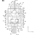
- FIG. FIG. 3 is a plan view seen from the Z1 direction of FIG. 2
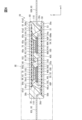
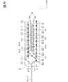
- 4 is a cross-sectional view taken along line IV-IV of FIG. 3
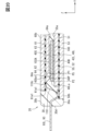
- FIG. 4 is a cross-sectional view taken along line V-V of FIG. 3
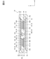
- FIG. 4 is a cross-sectional view taken along line VI-VI of FIG. 3
- FIG. 4 is a cross-sectional view taken along line VII-VII of FIG. 3
- FIG. FIG. 3 is a plan view showing a state in which a semiconductor element is mounted on a substrate
- FIG. 4 is a plan view showing a circuit pattern of a substrate on the drain electrode side;
- FIG. 4 is a plan view showing a circuit pattern of a substrate on the source electrode side;
- 7 is an enlarged view of region XI in FIG. 6.
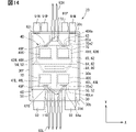
- FIG. It is sectional drawing which shows a modification. It is sectional drawing which shows a modification. It is a top view which shows a modification. It is a top view which shows a modification. It is a sectional view showing an example of a semiconductor device concerning a 2nd embodiment. It is sectional drawing which shows a manufacturing method. It is a sectional view showing another example of a semiconductor device. It is a figure which shows the effect of inductance reduction. It is a figure which shows a modification.
- FIG. 22 is a plan view of FIG. 21 viewed from the Z2 direction; 23 is a cross-sectional view taken along line XXIII-XXIII of FIG. 22; FIG. 23 is a cross-sectional view taken along line XXIV-XXIV of FIG. 22; FIG.
- the semiconductor device of this embodiment is applied, for example, to a power conversion device for a moving body that uses a rotating electrical machine as a drive source.
- Mobile objects include, for example, electric vehicles such as electric vehicles (EV), hybrid vehicles (HV), and plug-in hybrid vehicles (PHV), flying vehicles such as drones, ships, construction machinery, and agricultural machinery.
- EV electric vehicles
- HV hybrid vehicles
- PSV plug-in hybrid vehicles
- flying vehicles such as drones, ships, construction machinery, and agricultural machinery.
- a vehicle drive system 1 includes a DC power supply 2 , a motor generator 3 , and a power conversion device 4 .
- the DC power supply 2 is a DC voltage source composed of a rechargeable secondary battery. Secondary batteries are, for example, lithium ion batteries and nickel metal hydride batteries.
- the motor generator 3 is a three-phase alternating-current rotating electric machine. The motor generator 3 functions as a vehicle drive source, that is, as an electric motor. The motor generator 3 functions as a generator during regeneration.
- the power converter 4 performs power conversion between the DC power supply 2 and the motor generator 3 .
- the power conversion device 4 includes a power conversion circuit.
- the power conversion device 4 of this embodiment includes a smoothing capacitor 5 and an inverter 6 that is a power conversion circuit.
- the smoothing capacitor 5 mainly smoothes the DC voltage supplied from the DC power supply 2 .
- the smoothing capacitor 5 is connected to a P line 7 that is a power supply line on the high potential side and an N line 8 that is a power supply line on the low potential side.
- the P line 7 is connected to the positive pole of the DC power supply 2 and the N line 8 is connected to the negative pole of the DC power supply 2 .
- the positive terminal of smoothing capacitor 5 is connected to P line 7 between DC power supply 2 and inverter 6 .
- the negative electrode of smoothing capacitor 5 is connected to N line 8 between DC power supply 2 and inverter 6 .
- a smoothing capacitor 5 is connected in parallel with the DC power supply 2 .
- the P line 7 and N line 8 are sometimes referred to as power supply lines 7,8.
- the inverter 6 is a DC-AC conversion circuit. Inverter 6 converts the DC voltage into a three-phase AC voltage and outputs it to motor generator 3 according to switching control by a control circuit (not shown). Thereby, the motor generator 3 is driven to generate a predetermined torque. During regenerative braking of the vehicle, inverter 6 converts the three-phase AC voltage generated by motor generator 3 in response to the torque from the wheels into DC voltage according to switching control by the control circuit, and outputs the DC voltage to P line 7 . Thus, inverter 6 performs bidirectional power conversion between DC power supply 2 and motor generator 3 .
- the inverter 6 is configured with upper and lower arm circuits 9 for three phases.
- the upper and lower arm circuits 9 are sometimes called legs.
- the upper and lower arm circuits 9 each have an upper arm 9H and a lower arm 9L.
- the upper arm 9H and the lower arm 9L are connected in series between the P line 7 and the N line 8 with the upper arm 9H on the P line 7 side.
- a connection point between the upper arm 9 ⁇ /b>H and the lower arm 9 ⁇ /b>L is connected to a corresponding phase winding 3 a in the motor generator 3 via an output line 10 .
- Inverter 6 has six arms. Each arm is configured with a switching element. At least part of each of P line 7, N line 8 and output line 10 is formed of a conductive member such as a bus bar.
- an n-channel MOSFET 11 is used as a switching element that configures each arm.
- the number of switching elements forming each arm is not particularly limited. One or more may be used.
- MOSFET is an abbreviation for Metal Oxide Semiconductor Field Effect Transistor.
- each arm has two MOSFETs 11 in this embodiment.
- Two MOSFETs 11 forming one arm are connected in parallel.
- the drains of two MOSFETs 11 connected in parallel are connected to the P line 7 in the upper arm 9H.
- the sources of two MOSFETs 11 connected in parallel are connected to the N line 8 in the lower arm 9L.
- the sources of the two MOSFETs 11 connected in parallel on the upper arm 9H and the drains of the two MOSFETs 11 connected in parallel on the lower arm 9L are connected to each other.
- the two MOSFETs 11 connected in parallel are turned on and off at the same timing by a common gate driving signal (driving voltage).
- a freewheeling diode 12 is connected in antiparallel to each of the MOSFETs 11 .
- the diode 12 may be a parasitic diode (body diode) of the MOSFET 11 or may be provided separately from the parasitic diode.
- the anode of diode 12 is connected to the source of corresponding MOSFET 11, and the cathode is connected to the drain.
- the upper and lower arm circuits 9 for one phase are provided by one semiconductor device 20 . Details of the semiconductor device 20 will be described later.
- the power conversion device 4 may further include a converter as a power conversion circuit.
- a converter is a DC-DC conversion circuit that converts a DC voltage into DC voltages of different values.
- the converter is provided between the DC power supply 2 and the smoothing capacitor 5 .
- the converter includes, for example, a reactor and the upper and lower arm circuits 9 described above. According to this configuration, it is possible to step up and down.
- the power conversion device 4 may include a filter capacitor that removes power noise from the DC power supply 2 .
- a filter capacitor is provided between the DC power supply 2 and the converter.
- the power conversion device 4 may include a driving circuit for switching elements that constitute the inverter 6 and the like.
- the drive circuit supplies a drive voltage to the gate of the MOSFET 11 of the corresponding arm based on the drive command from the control circuit.
- the drive circuit drives the corresponding MOSFET 11 by applying a drive voltage, that is, turns it on and off.
- a driving circuit is sometimes referred to as a driver.
- the power conversion device 4 may include a control circuit for switching elements.
- the control circuit generates a drive command for operating the MOSFET 11 and outputs it to the drive circuit.
- the control circuit generates a drive command based on, for example, a torque request input from a host ECU (not shown) and signals detected by various sensors.
- ECU is an abbreviation for Electronic Control Unit.
- Various sensors include, for example, current sensors, rotation angle sensors, and voltage sensors.
- the current sensor detects a phase current flowing through each phase winding 3a.
- the rotation angle sensor detects the rotation angle of the rotor of motor generator 3 .
- a voltage sensor detects the voltage across the smoothing capacitor 5 .
- the control circuit comprises, for example, a processor and memory.
- the control circuit outputs, for example, a PWM signal as the drive command.
- PWM is an abbreviation for Pulse Width Modulation.
- FIG. 2 is a perspective view of the semiconductor device 20.
- FIG. FIG. 3 is a plan view of FIG. 2 viewed from the Z1 direction.
- FIG. 3 is a transparent view showing the internal structure. A portion covered with the sealing body 30 is indicated by a dashed line.
- 4 is a cross-sectional view taken along line IV-IV of FIG. 3.
- FIG. 5 is a cross-sectional view taken along line VV in FIG. 3.
- FIG. 6 is a cross-sectional view taken along line VI-VI of FIG. 3.
- FIG. 7 is a cross-sectional view taken along line VII-VII of FIG. 3.
- FIG. 8 is a plan view showing a state in which the semiconductor element 40 is mounted on the substrate 50.
- FIG. 8 is a diagram excluding the sealing body 30 and the substrate 60 from FIG. 9 is a plan view showing the circuit pattern of the surface metal body 52 on the substrate 50.
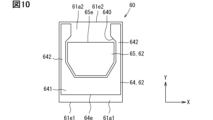
- FIG. FIG. 10 is a plan view showing the circuit pattern of the surface metal body 62 on the substrate 60.
- the plate thickness direction of the semiconductor element 40 is defined as the Z direction.
- the direction in which the plurality of semiconductor elements 40 arranged side by side is perpendicular to the Z direction is defined as the X direction.
- the direction in which the plurality of semiconductor elements 40 connected in parallel are arranged is the X direction.
- a direction perpendicular to both the Z direction and the X direction is defined as the Y direction.
- a planar shape is defined as a planar shape viewed from the Z direction, in other words, a planar shape along the XY plane defined by the X and Y directions.
- a planar view from the Z direction may be simply referred to as a planar view.
- the semiconductor device 20 constitutes one of the upper and lower arm circuits 9 described above, that is, the upper and lower arm circuits 9 for one phase.
- the semiconductor device 20 includes a sealing body 30 , a semiconductor element 40 , substrates 50 and 60 , conductive spacers 70 , arm connecting portions 80 and external connection terminals 90 .
- the semiconductor device 20 is sometimes called a semiconductor module, power card, or the like.
- the encapsulant 30 encloses part of other elements that constitute the semiconductor device 20 .
- the rest of the other elements are exposed outside the encapsulant 30 .
- Sealing body 30 is made of resin, for example.
- An example of the resin is an epoxy resin.
- the sealing body 30 is made of resin and is molded by, for example, a transfer molding method. Such a sealing body 30 is sometimes referred to as a sealing resin body, mold resin, resin molded body, or the like.
- Sealing body 30 may be formed using gel, for example. The gel is filled (arranged) in opposing regions of the pair of substrates 50 and 60, for example.
- the sealing body 30 has a substantially rectangular planar shape.
- the sealing body 30 has one surface 30a and a back surface 30b opposite to the one surface 30a in the Z direction as surfaces forming an outline.
- One surface 30a and back surface 30b are, for example, flat surfaces. It also has side surfaces 30c, 30d, 30e, and 30f that connect the one surface 30a and the back surface 30b.
- the side surface 30c is a surface from which the power supply terminal 91 and the signal terminal 93H of the external connection terminals 90 protrude.
- the side surface 30d is a surface opposite to the side surface 30c in the Y direction.
- the side surface 30d is a surface from which the output terminal 92 and the signal terminal 93L protrude.
- the side surfaces 30e and 30f are surfaces from which the external connection terminals 90 do not protrude.
- the side surface 30e is a surface opposite to the side surface 30f in the X direction.
- the semiconductor element 40 is formed by forming a switching element on a semiconductor substrate made of silicon (Si), a wide bandgap semiconductor having a wider bandgap than silicon, or the like.
- Wide bandgap semiconductors include, for example, silicon carbide (SiC), gallium nitride (GaN), gallium oxide (Ga2O3), and diamond.
- the semiconductor element 40 may be called a power element, a semiconductor chip, or the like.
- the semiconductor element 40 of this embodiment is formed by forming the n-channel MOSFET 11 on a semiconductor substrate made of SiC.
- the MOSFET 11 has a vertical structure so that the main current flows in the plate thickness direction of the semiconductor element 40 (semiconductor substrate), that is, in the Z direction.
- the semiconductor element 40 has main electrodes of switching elements on both sides in the Z direction, which is the thickness direction of the semiconductor element 40 .
- a main electrode it has a drain electrode 40D on one surface and a source electrode 40S on the back surface opposite to the one surface in the Z direction. A main current flows between the drain electrode 40D and the source electrode 40S.
- Diode 12 When the diode 12 is a parasitic diode, the source electrode 40S doubles as the anode electrode, and the drain electrode 40D doubles as the cathode electrode. Diode 12 may be configured on a separate chip from MOSFET 11 .
- the drain electrode 40D is the main electrode on the high potential side, and the source electrode 40S is the main electrode on the low potential side.
- the semiconductor element 40 has a substantially rectangular planar shape, for example, a square shape. As shown in FIGS. 3 and 8, the semiconductor element 40 has pads 40P, which are electrodes for signals, on its back surface. The pad 40P is formed at a position different from the source electrode 40S on the back surface. Pad 40P includes at least a gate pad. The semiconductor element 40 of this embodiment has four pads 40P. Pad 40P includes gate pad GP, Kelvin source pad KSP, anode pad AP, and cathode pad KP as shown in FIG.
- the gate pad GP is a pad 40P for applying a drive voltage to the gate electrode of the MOSFET 11. That is, the gate pad GP is a gate electrode pad 40P that controls the main current flowing between the drain electrode 40D and the source electrode 40S, which are the main electrodes.
- the Kelvin source pad KSP is a pad 40P for detecting the source potential of the MOSFET 11, that is, the potential of the source electrode 40S.
- the anode pad AP is a pad 40P for detecting the anode potential of a temperature sensitive diode (not shown) included in the semiconductor element 40 .
- the cathode pad KP is a pad 40P for detecting the cathode potential of the temperature sensitive diode.
- the gate pad GP, anode pad AP, and cathode pad KP are electrically separated from the source electrode 40S.
- Kelvin source pad KSP is electrically connected to source electrode 40S.
- the gate pad GP, the Kelvin source pad KSP, the anode pad AP, and the cathode pad KP are arranged in this order in the X direction.
- the source electrode 40S and pad 40P are exposed from a protective film (not shown) formed on the back surface of the semiconductor substrate.
- the drain electrode 40D is formed over substantially the entire surface.
- the source electrode 40S is formed on a portion of the back surface of the semiconductor element 40. As shown in FIG. In plan view, the drain electrode 40D has a larger area than the source electrode 40S.
- the drain electrode 40D corresponds to the first main electrode, and the source electrode 40S corresponds to the second main electrode.
- the semiconductor device 20 includes a plurality of semiconductor elements 40 configured as described above.
- the plurality of semiconductor elements 40 includes a semiconductor element 40H forming the upper arm 9H and a semiconductor element 40L forming the lower arm 9L.
- the semiconductor element 40H is sometimes called an upper arm element, and the semiconductor element 40L is sometimes called a lower arm element.
- the semiconductor element 40 of this embodiment includes two semiconductor elements 40H and two semiconductor elements 40L.
- the semiconductor element 40H includes a semiconductor element 41H as a first element and a semiconductor element 42H as a second element.
- the two semiconductor elements 40H (41H, 42H) are arranged in the X direction.
- Two semiconductor elements 40H arranged side by side in the X direction have a common structure.
- Two semiconductor elements 40H having a common structure are arranged side by side in the X direction in the same direction.
- the two semiconductor elements 40H are connected in parallel with each other.
- the semiconductor element 40L includes a semiconductor element 41L as a first element and a semiconductor element 42L as a second element.
- the two semiconductor elements 40L (41L, 42L) are arranged in the X direction.
- the two semiconductor elements 40L arranged side by side in the X direction have a common structure.
- the two semiconductor elements 40L having a common structure are arranged side by side in the X direction in the same direction.
- the two semiconductor elements 40L are connected in parallel with each other.
- all semiconductor elements 40 have a common structure.
- the arrangement of the semiconductor elements 41H and 42H and the arrangement of the semiconductor elements 41L and 42L have two-fold symmetry around the axis along the Z direction.
- the semiconductor element 40H and the semiconductor element 40L are arranged in the Y direction.
- the semiconductor device 20 has two rows of semiconductor elements 40H and 40L along the Y direction.
- Each semiconductor element 40 is arranged at substantially the same position in the Z direction.
- a drain electrode 40 ⁇ /b>D of each semiconductor element 40 faces the substrate 50 .
- a source electrode 40 ⁇ /b>S of each semiconductor element 40 faces the substrate 60 .
- the substrates 50 and 60 are arranged so as to sandwich the plurality of semiconductor elements 40 in the Z direction.
- the substrates 50 and 60 are arranged so that at least parts of them face each other in the Z direction.
- the substrates 50, 60 include all of the plurality of semiconductor elements 40 (40H, 40L) in plan view.
- the substrate 50 is arranged on the drain electrode 40D side with respect to the semiconductor element 40 .
- the substrate 60 is arranged on the source electrode 40S side with respect to the semiconductor element 40 .
- the substrate 50 is electrically connected to the drain electrode 40D and provides a wiring function, as will be described later.
- substrate 60 is electrically connected to source electrode 40S and provides a wiring function. Therefore, the substrates 50 and 60 are sometimes referred to as wiring members, wiring substrates, and the like.
- Substrate 50 is sometimes referred to as the drain substrate and substrate 60 is sometimes referred to as the source substrate.
- the substrates 50 and 60 provide a heat dissipation function for dissipating heat generated by the semiconductor element 40 . For this reason, the substrates 50 and 60 are sometimes called heat dissipation members.
- the substrate 50 corresponds to a first wiring member.
- the substrate 60 is a second wiring member electrically connected to the second main electrode.
- the substrate 50 has a facing surface 50a facing the semiconductor element 40 and a back surface 50b opposite to the facing surface 50a.
- the substrate 50 includes an insulating base material 51 , a front metal body 52 and a back metal body 53 .
- the substrate 60 has a facing surface 60a facing the semiconductor element 40 and a back surface 60b opposite to the facing surface 60a.
- the substrate 60 includes an insulating base material 61 , a front metal body 62 and a back metal body 63 .
- the surface metal bodies 52 and 62 and the back metal bodies 53 and 63 may be simply referred to as metal bodies 52, 53, 62 and 63 below.
- the substrate 50 is a substrate in which an insulating base material 51 and metal bodies 52 and 53 are laminated.
- the substrate 60 is a substrate in which an insulating base material 61 and metal bodies 62 and 63 are laminated.
- the insulating base material 51 electrically separates the front metal body 52 and the back metal body 53 .
- the insulating base material 61 electrically isolates the front metal body 62 and the back metal body 63 .
- the insulating base materials 51 and 61 are sometimes called insulating layers.
- the insulating base materials 51 and 61 are made of resin or inorganic ceramic.
- As the resin for example, an epoxy resin, a polyimide resin, or the like can be used.
- As the ceramic for example, Al2O3 (alumina), Si3N4 (silicon nitride), or the like can be used.
- the substrates 50 and 60 are sometimes called metal-resin substrates.
- the substrates 50, 60 are sometimes referred to as metal-ceramic substrates.
- an inorganic filler may be included in the resin in order to improve heat dissipation, insulation, and the like.
- the coefficient of linear expansion may be adjusted by adding a filler.
- fillers include Al2O3, SiO2 (silicon dioxide), AlN (aluminum nitride), and BN (boron nitride).
- the insulating base materials 51 and 61 may contain only one type of filler, or may contain a plurality of types.
- the thickness of each of the insulating bases 51 and 61 is preferably about 50 ⁇ m to 300 ⁇ m. In the case of ceramics, the thickness of the insulating bases 51 and 61 is preferably about 200 ⁇ m to 500 ⁇ m.
- the front surfaces of the insulating bases 51 and 61 are inner surfaces, that is, surfaces on the semiconductor element 40 side, and the back surfaces opposite to the front surfaces in the Z direction are outer surfaces.
- the insulating base materials 51 and 61 may have a common (same) material configuration, or may have different material configurations.
- resin-based insulating base materials 51 and 61 are employed, and the material configuration is common.
- the linear expansion coefficients of the insulating base materials 51 and 61 are adjusted to substantially the same value as that of the sealing body 30 by adding a filler to the resin.
- the linear expansion coefficients of the insulating bases 51 and 61 and the sealing body 30 are close to those of the metal (Cu) forming the metal bodies 52 , 53 , 62 and 63 .
- the metal bodies 52, 53, 62, 63 are provided as metal plates or metal foils, for example.
- the metal bodies 52, 53, 62, and 63 are made of a metal such as Cu or Al that has good electrical and thermal conductivity.
- the thickness of each of the metal bodies 52, 53, 62, 63 is, for example, approximately 0.1 mm to 3 mm.
- the surface metal body 52 is arranged on the surface of the insulating base material 51 in the Z direction.
- the back metal body 53 is arranged on the back surface of the insulating base material 51 .
- the surface metal body 62 is arranged on the surface of the insulating base material 61 in the Z direction.
- the back metal body 63 is arranged on the back surface of the insulating base material 61 .
- the thickness relationship between the surface metal bodies 52, 62 and the back metal bodies 53, 63 is not particularly limited.
- the thickness of the surface metal body 52 may be greater than that of the back metal body 53 or may be substantially equal to that of the back metal body 53 .
- the thickness of the surface metal body 52 may be thinner than that of the back metal body 53 .
- the thickness of the surface metal body 62 may be greater than that of the back metal body 63 or may be substantially equal to that of the back metal body 63 .
- the thickness of the surface metal body 62 may be thinner than that of the back surface metal body 63 .
- the relationship between the thicknesses of the surface metal bodies 52 and 62 is not particularly limited, and the relationship between the thicknesses of the backside metal bodies 53 and 63 is also not particularly limited.
- the surface metal bodies 52, 62 are patterned.
- the surface metallurgy 52, 62 provides wiring or circuitry. Therefore, the surface metal bodies 52 and 62 are sometimes referred to as circuit patterns, wiring layers, circuit conductors, and the like.
- the surface metal bodies 52 and 62 may have a plating film of Ni or Au on the metal surface.
- the pattern of the surface metal bodies 52, 62 is sometimes referred to as a circuit pattern.
- the surface of the surface metal body 52 and the non-arranged area of the surface metal body 52 on the surface of the insulating base material 51 form the facing surface 50a of the substrate 50 .
- the surface of the surface metal body 62 and the non-arrangement area of the surface metal body 62 on the surface of the insulating base material 61 form the facing surface 60 a of the substrate 60 .
- surface metal bodies 52 and 62 patterned into a predetermined shape by press working, etching, or the like are prepared and adhered to a laminate having a two-layer structure of insulating base materials 51 and 61 and back metal bodies 53 and 63 to form a substrate. 50, 60 may be formed.
- the surface metal bodies 52 and 62 may be patterned by cutting or etching after forming a three-layer laminate of the surface metal bodies 52 and 62, the insulating substrates 51 and 61, and the back metal bodies 53 and 63.
- the surface metal body 52 has a P wiring 54 and a relay wiring 55, as shown in FIGS.
- the P wiring 54 and the relay wiring 55 are electrically separated by a predetermined interval (gap). This gap is filled with a sealing body 30 .
- the P wiring 54 has a facing surface 54a
- the relay wiring 55 has a facing surface 55a.
- the P wiring 54 is connected to a P terminal 91P and a drain electrode 40D of the semiconductor element 40H, which will be described later.
- the P wiring 54 electrically connects the P terminal 91P and the drain electrode 40D of the semiconductor element 40H.
- the P wiring 54 electrically connects the drain electrode 40D of the semiconductor element 41H and the drain electrode 40D of the semiconductor element 42H.
- the relay wiring 55 is connected to the drain electrode 40D of the semiconductor element 40L, the arm connecting portion 80, and the output terminal 92.
- the relay wiring 55 electrically connects the arm connecting portion 80 and the drain electrode 40D of the semiconductor element 40L.
- the relay wiring 55 electrically connects the output terminal 92 with the source electrode 40S of the semiconductor element 40H and the drain electrode 40D of the semiconductor element 40L.
- the relay wiring 55 electrically connects the drain electrode 40D of the semiconductor element 41L and the drain electrode 40D of the semiconductor element 42L.
- the P wiring 54 and the relay wiring 55 are arranged side by side in the Y direction. In the Y direction, the P wiring 54 is arranged on the power supply terminal 91 side, and the relay wiring 55 is arranged on the output terminal 92 side. The P wiring 54 is arranged on the side surface 30c side of the sealing body 30, and the relay wiring 55 is arranged on the side surface 30d side.
- the P wiring 54 has a cutout 540 .
- the notch 540 is open on one of four sides of a substantially rectangular plane having the X direction as the longitudinal direction.
- the notch 540 is provided substantially in the center in the X direction on the side facing the side surface 30c.
- the P wiring 54 has a base portion 541 and a pair of extension portions 542 .
- a base 541 and a pair of extensions 542 define a notch 540 .
- the P-wiring 54 has a substantially U-shaped (concave-shaped) plane shape.
- the base portion 541 is a portion closer to the relay wiring 55 than the notch 540 and the extended portion 542 in the Y direction, and has a substantially rectangular planar shape.
- the base 541 overlaps the semiconductor element 40H in plan view. That is, the two semiconductor elements 40H (41H, 42H) are arranged on the base portion 541. As shown in FIG. A drain electrode 40D of each semiconductor element 40H is connected to the base portion 541 .
- the two extended portions 542 extend from the base portion 541 in the same direction, specifically the Y direction, toward the side surface 30c of the sealing body 30 .
- One of the extended portions 542 is continuous with one end of the base portion 541 in the X direction, and the other is continuous with the other end of the base portion 541 .
- Both ends of the U-shape of the P wiring 54, that is, the ends of the two extended portions 542 on the side opposite to the base portion 541 are substantially at the same position in the Y direction.
- a pair of extending portions 542 sandwich the notch 540 in the X direction.
- the base portion 541 is longer than the depth of the notch 540 and the extending portion 542 .
- the relay wiring 55 also has a notch 550.
- the notch 550 is open on one of the four sides of the substantially rectangular plane.
- the notch 550 is provided substantially in the center in the X direction on the side facing the side surface 30d. That is, the surface metal body 52 has a notch 540 at one end in the Y direction and a notch 550 at the other end.
- the relay wiring 55 has a base portion 551 and a pair of extension portions 552 .
- a base 551 and a pair of extensions 552 define a notch 550 .
- the relay wiring 55 has a substantially U-shaped (concave-shaped) plane shape.
- the base portion 551 is a portion closer to the P wiring 54 than the notch 550 and the extended portion 552 in the Y direction, and has a substantially rectangular planar shape.
- the base 551 overlaps the semiconductor element 40L in plan view. That is, the two semiconductor elements 40L (41L, 42L) are arranged on the base portion 551. As shown in FIG.
- a drain electrode 40 ⁇ /b>D of each semiconductor element 40 ⁇ /b>L is connected to the base 551 .
- the two extending portions 552 extend from the base portion 551 in the same direction, specifically the Y direction, toward the side surface 30 d of the sealing body 30 .
- One of the extended portions 552 continues near one end of the base portion 551 in the X direction, and the other extends near the other end of the base portion 551 .
- Both ends of the U-shape of the relay wiring 55 that is, the ends of the two extended portions 552 on the side opposite to the base portion 551 are substantially at the same position in the Y direction.
- the pair of extensions 552 sandwich the notch 550 in the X direction.
- the base portion 551 is longer than the depth of the notch 550 and the extending portion 552 .
- the surface metal body 62 has an N wiring 64 and a relay wiring 65, as shown in FIGS.
- the N wiring 64 and the relay wiring 65 are electrically separated by a predetermined interval (gap). This gap is filled with a sealing body 30 .
- the N wiring 64 has a facing surface 64a
- the relay wiring 65 has a facing surface 65a.
- the N wiring 64 is connected to an N terminal 91N and a source electrode 40S of the semiconductor element 40L, which will be described later.
- the N wiring 64 electrically connects the N terminal 91N and the source electrode 40S of the semiconductor element 40L.
- the N wiring 64 electrically connects the source electrode 40S of the semiconductor element 41L and the source electrode 40S of the semiconductor element 42L.
- the N wiring 64 is sometimes called a negative wiring, a low potential power supply wiring, or the like.
- the relay wiring 65 is connected to the source electrode 40S and the arm connecting portion 80 of the semiconductor element 40H.
- the relay wiring 65 electrically connects the source electrode 40S of the semiconductor element 40H and the arm connection portion 80 .
- the relay wiring 65 electrically connects the source electrode 40S of the semiconductor element 41H and the source electrode 40S of the semiconductor element 42H.
- the N wiring 64 also has a notch 640.
- the notch 640 is open on one of the four sides of the substantially rectangular plane.
- the notch 640 is provided substantially in the center in the X direction on the side facing the side surface 30c.
- the N wiring 64 has a base portion 641 and a pair of extension portions 642 .
- a base 641 and a pair of extensions 642 define a notch 640 .
- the N-wiring 64 has a substantially U-shaped (concave-shaped) plane shape.
- the base portion 641 is a portion closer to the side surface 30d than the notch 640 and the extension portion 642 in the Y direction.
- the base portion 641 has a substantially rectangular planar shape whose longitudinal direction is the X direction.
- the base 641 is arranged side by side with the relay wiring 65 in the Y direction.
- the base 641 overlaps the relay wiring 55 in plan view.
- the source electrode 40S of each semiconductor element 40L is connected to the base 641. As shown in FIG.
- the two extending portions 642 extend from the base portion 641 in the same direction, specifically the Y direction, toward the side surface 30c of the sealing body 30 .
- One of the extension portions 642 is connected to the vicinity of one end of the base portion 641 in the X direction, and the other is connected to the vicinity of the other end of the base portion 641 .
- Both ends of the U-shape of the N wiring 64, that is, the ends of the two extended portions 642 on the side opposite to the base portion 641 are substantially at the same position in the Y direction.
- the pair of extensions 642 form both ends of the surface metal body 62 in the X direction.
- the pair of extensions 642 are arranged near the edge of the substrate 60 .
- a part of each of the pair of extended portions 642 overlaps the P wiring 54 in plan view.
- the extension portion 642 is longer than the base portion 641 in the Y direction.
- the relay wiring 65 is arranged side by side with the N wiring 64, specifically the base 641, in the Y direction. In the Y direction, the relay wiring 65 is arranged at a position close to the side surface 30c of the sealing body 30, and the base portion 641 is arranged at a position close to the side surface 30d.
- the relay wiring 65 is arranged between the pair of extension portions 642 in the X direction.
- the relay wiring 65 is sandwiched between a pair of extension portions 642 .
- the relay wiring 65 is arranged inside the notch 640 .
- the relay wiring 65 is arranged with a predetermined interval (gap) from the N wiring 64 .
- a part of the relay wiring 65 overlaps the P wiring 54 and another part of the relay wiring 65 overlaps the relay wiring 55 in plan view.
- a source electrode 40S of each semiconductor element 40H is connected to a relay wiring 65 .
- the details of the arrangement of the surface metal bodies 62 (the N wirings 64 and the relay wirings 65) will be described later.
- the back metal bodies 53 and 63 are electrically separated from the circuit including the semiconductor element 40 and the front metal bodies 52 and 62 by the insulating substrates 51 and 61 .
- the back metal bodies 53 and 63 are sometimes referred to as metal base substrates. Heat generated by the semiconductor element 40 is transmitted to the back metal bodies 53 and 63 via the front metal bodies 52 and 62 and the insulating base materials 51 and 61 .
- the back metal bodies 53, 63 provide a heat dissipation function.
- the back metal bodies 53 and 63 of this embodiment have a substantially rectangular planar shape.
- the back metal bodies 53 and 63 are so-called solid conductors that are arranged on almost the entire back surface of the insulating substrates 51 and 61 .
- the back metal bodies 53 and 63 may be patterned so as to match the front metal bodies 52 and 62 in plan view.
- the back metal bodies 53 and 63 of the present embodiment are arranged over substantially the entire back surface of the corresponding insulating bases 51 and 61 . At least one of the back metal bodies 53 and 63 may be exposed from the sealing body 30 in order to further enhance the heat dissipation effect.
- the back metal body 53 is exposed from the one surface 30a of the sealing body 30, and the back metal body 63 is exposed from the back surface 30b.
- the exposed surface of the back metal body 53 is substantially flush with the one surface 30a.
- the exposed surface of the back metal body 63 is substantially flush with the back surface 30b.
- Backside metal bodies 53 and 63 form backside surfaces 50b and 60b of substrates 50 and 60, respectively.
- the conductive spacer 70 provides a spacer function to secure a predetermined distance between the semiconductor element 40 and the substrate 60.
- the conductive spacers 70 ensure wire height for electrically connecting the corresponding signal terminals 93 to the pads 40P of the semiconductor element 40 .
- the conductive spacer 70 is located in the middle of the electrical and thermal conduction path between the source electrode 40S of the semiconductor element 40 and the substrate 60, and provides wiring and heat dissipation functions.
- the conductive spacer 70 contains a metal material such as Cu that has good electrical and thermal conductivity.
- the conductive spacer 70 may have a plated film on its surface.
- the conductive spacer 70 is sometimes called a terminal, a terminal block, a metal block body, or the like.
- the semiconductor device 20 includes the same number of conductive spacers 70 as the semiconductor elements 40 . Specifically, four conductive spacers 70 are provided. Conductive spacers 70 are individually connected to semiconductor elements 40 .
- the conductive spacer 70 is a columnar body having a size substantially the same as or slightly smaller than that of the source electrode 40S in plan view.
- the arm connecting portion 80 electrically connects the relay wirings 55 and 65 . That is, the arm connecting portion 80 electrically connects the upper arm 9H and the lower arm 9L.
- the arm connecting portion 80 is provided between the semiconductor element 40H and the semiconductor element 40L in the Y direction.
- the arm connecting portion 80 is provided in an overlapping region between the relay wiring 55 and the relay wiring 65 in plan view.
- the arm connecting portion 80 of the present embodiment includes a joint portion 81 and a bonding material 103 which will be described later.
- the joint portion 81 is a metal columnar body provided separately from the surface metal bodies 52 and 62 . Such a joint portion 81 is sometimes called a joint terminal.
- a bonding material 103 is interposed between one end of the joint portion 81 and the relay wiring 55 , and a bonding material 103 is interposed between the other end and the relay wiring 65 .
- the joint portion 81 may be integrally connected to at least one of the surface metal bodies 52 and 62.
- the joint portion 81 may be provided integrally with the surface metal bodies 52 and 62 as part of the substrates 50 and 60 .
- joint portion 81 is a convex portion of surface metal body 62 (relay wiring 65).
- the arm connecting portion 80 may be configured without the joint portion 81 .
- the arm connecting portion 80 may be configured to include only the bonding material 103 .
- the external connection terminal 90 is a terminal for electrically connecting the semiconductor device 20 to an external device.
- the external connection terminal 90 is formed using a metal material with good conductivity such as copper.
- the external connection terminal 90 is, for example, a plate material.
- the external connection terminals 90 are sometimes called leads.
- the external connection terminal 90 includes a power terminal 91 , an output terminal 92 and a signal terminal 93 .
- the power terminal 91 has a P terminal 91P and an N terminal 91N.
- P-terminal 91P, N-terminal 91N, and output terminal 92 are main terminals electrically connected to the main electrodes of semiconductor element 40 .
- the signal terminals 93 include a signal terminal 93H on the upper arm 9H side and a signal terminal 93L on the lower arm 9L side.
- the power terminal 91 is an external connection terminal 90 electrically connected to the power lines 7 and 8 described above.
- P terminal 91P is electrically connected to the positive terminal of smoothing capacitor 5 .
- the P terminal 91P is sometimes called a positive electrode terminal, a high potential power supply terminal, or the like.
- the P terminal 91P is connected to the P wiring 54 of the surface metal body 52 . In other words, the P terminal 91P is connected to the drain electrode 40D of the semiconductor element 40H forming the upper arm 9H.
- the P terminal 91P is connected near one end of the P wiring 54 in the Y direction.
- the P terminal 91P extends in the Y direction from a connection portion (joint portion) with the P wiring 54, and protrudes outside the sealing body 30 from near the center in the Z direction on the side surface 30c.
- the semiconductor device 20 of this embodiment has two P terminals 91P. As shown in FIG. 8, one of the P terminals 91P is connected to one of the pair of extensions 542, and the other is connected to the other one of the pair of extensions 542. As shown in FIG.
- the P terminal 91P is arranged at a position close to the notch 540 in each of the extended portions 542, that is, inward, so as to be adjacent to the N terminal 91N in plan view.
- the two P terminals 91P are arranged side by side in the X direction.
- the two P terminals 91P are arranged at substantially the same position in the Z direction.
- the N terminal 91N is electrically connected to the negative terminal of the smoothing capacitor 5 .
- the N terminal 91N is sometimes called a negative electrode terminal, a low potential power supply terminal, or the like.
- the N terminal 91N is connected to the N wiring 64 of the surface metal body 62 . In other words, the N terminal 91N is connected to the source electrode 40S of the semiconductor element 40L forming the lower arm 9L.
- the N terminal 91N is connected near one end of the N wiring 64 in the Y direction.
- the N terminal 91N extends in the Y direction from the junction with the N wiring 64, and protrudes outside the sealing body 30 from near the center in the Z direction on the side surface 30c.
- the semiconductor device 20 has two N terminals 91N.
- One of the N terminals 91N is connected to one of the pair of extension portions 642, and the other is connected to the other one of the pair of extension portions 642.
- the two N terminals 91N are arranged side by side in the X direction.
- the two N terminals 91N are arranged at substantially the same position in the Z direction.
- the two N terminals 91N are arranged outside the two P terminals 91P in the X direction.
- one of the N terminals 91N is arranged near one of the P terminals 91P, and the other one of the N terminals 91N is arranged near the other one of the P terminals 91P.
- the N terminal 91N and the P terminal 91P which are adjacent in the X direction, face each other at a portion including a portion protruding from the sealing body 30 at their sides.
- the output terminal 92 is electrically connected to the corresponding phase winding 3 a (stator coil) of the motor generator 3 .
- the output terminal 92 is sometimes called an O terminal, an AC terminal, or the like.
- the output terminal 92 is connected to the relay wiring 55 of the surface metal body 52 on the substrate 50 . That is, the output terminal 92 is connected to the connection point between the upper arm 9H and the lower arm 9L.
- the output terminal 92 is connected near one end of the relay wiring 55 in the Y direction.
- the output terminal 92 extends in the Y direction from the junction with the relay wiring 55 and protrudes outside the sealing body 30 from near the center in the Z direction on the side surface 30d.
- the semiconductor device 20 has two output terminals 92 .
- One of the output terminals 92 is connected to one of the pair of extensions 552 and the other is connected to the other one of the pair of extensions 552 .
- the two output terminals 92 are arranged side by side in the X direction.
- the two output terminals 92 are arranged at substantially the same position in the Z direction.
- the signal terminal 93 is electrically connected to a circuit board (not shown) including a drive circuit.
- the signal terminal 93H is electrically connected to the pad 40P of the semiconductor element 40H through the bonding wire 110.
- the number of signal terminals 93H is not particularly limited.
- the signal terminal 93H includes at least a terminal for applying a driving voltage to the gate electrode of the semiconductor element 40H.
- the semiconductor device 20 of this embodiment has two signal terminals 93H.
- the signal terminal 93H is arranged at a position overlapping the notch 540 of the P wiring 54 in plan view. In the signal terminal 93 ⁇ /b>H, the joint with the bonding wire 110 faces the insulating base material 51 instead of the surface metal body 52 .
- the two signal terminals 93H are arranged side by side in the X direction.
- the signal terminal 93H extends in the Y direction from the joint with the bonding wire 110, and protrudes outside the sealing body 30 from near the center in the Z direction on the side surface 30c. At least part of the projecting portion of the signal terminal 93 ⁇ /b>H extends in the same direction as the power terminal 91 .
- the signal terminal 93H is arranged between the two P terminals 91P in the X direction. That is, the external connection terminals 90 protruding from the side surface 30c are arranged in the order of the N terminal 91N, the P terminal 91P, the two signal terminals 93H, the P terminal 91P, and the N terminal 91N in the X direction.
- the signal terminal 93H includes a gate terminal 93G and a Kelvin source terminal 93KS.
- the two signal terminals 93H are arranged in the order of the gate terminal 93G and the Kelvin source terminal 93KS in the direction from the semiconductor element 42H to the semiconductor element 41H.
- the gate terminal 93G is connected via a bonding wire 110 to the gate pad GP of each semiconductor element 40H.
- Kelvin source terminal 93KS is connected via bonding wire 110 to Kelvin source pad KSP of each semiconductor element 40H.
- the signal terminal 93L is electrically connected to the pad 40P of the semiconductor element 40L via the bonding wire 110.
- the signal terminal 93L includes at least a terminal for applying a drive voltage to the gate electrode of the semiconductor element 40L.
- the semiconductor device 20 of this embodiment has four signal terminals 93L.
- the signal terminal 93L is arranged at a position overlapping the notch 550 of the relay wiring 55 in plan view.
- the joint with the bonding wire 110 faces the insulating base material 51 instead of the surface metal body 52 .
- the four signal terminals 93L are arranged side by side in the X direction.
- the signal terminal 93L extends in the Y direction from the joint with the bonding wire 110, and protrudes outside the sealing body 30 from near the center in the Z direction on the side surface 30d. At least part of the projecting portion of the signal terminal 93L extends in the same direction as the output terminal 92 .
- the signal terminal 93L is arranged between the two output terminals 92 in the X direction. That is, the external connection terminals 90 projecting from the side surface 30d are arranged in the order of the output terminal 92, the four signal terminals 93L, and the output terminal 92 in the X direction.
- the four signal terminals 93L are arranged in the space between the output terminals 92. As shown in FIG.
- the signal terminal 93L includes a gate terminal 93G, a Kelvin source terminal 93KS, an anode terminal 93A and a cathode terminal 93K.
- the four signal terminals 93L are arranged in the order of gate terminal 93G, Kelvin source terminal 93KS, anode terminal 93A, and cathode terminal 93K in the direction from semiconductor element 42L to semiconductor element 41L.
- the arrangement of the four signal terminals 93L corresponds to the arrangement of the pads 40P of the semiconductor element 41L.
- the gate terminal 93G is connected via a bonding wire 110 to the gate pad GP of each semiconductor element 40L.
- the Kelvin source terminal 93KS is connected via a bonding wire 110 to the Kelvin source pad KSP of each semiconductor element 40L.
- the anode terminal 93A is connected via a bonding wire 110 to an anode pad AP of the semiconductor element 41L.
- the cathode terminal 93K is connected via a bonding wire 110 to the cathode pad KP of the semiconductor element 41L.
- the semiconductor device 20 has two signal terminals 93H and four signal terminals 93L as the signal terminals 93.
- the signal terminal 93H is arranged so as to sandwich the semiconductor element 40 with the signal terminal 93L in the Y direction.
- the two signal terminals 93H are arranged side by side in the X direction together with the four power supply terminals 91 (91P, 91N).
- the four signal terminals 93L are arranged along with the two output terminals 92 in the X direction.
- Two signal terminals 93H and four signal terminals 93L are provided in order to suppress an increase in size in the X direction.
- the number of external connection terminals 90 is six on each of the side surfaces 30c and 30d.
- the Kelvin source terminal 93KS which is the signal terminal 93H, is connected to the anode pad AP of each semiconductor element 40H via the bonding wire 110 in order to suppress the potential floating state of the temperature sensitive diode. It is Alternatively, Kelvin source terminal 93KS may be connected to cathode pad KP of each semiconductor element 40H. Similarly, the Kelvin source terminal 93KS, which is the signal terminal 93L, is connected via a bonding wire 110 to the anode pad AP of the semiconductor element 42L. Alternatively, Kelvin source terminal 93KS may be connected to cathode pad KP of semiconductor element 42L.
- the drain electrode 40D of the semiconductor element 40 is bonded to the surface metal body 52 via the bonding material 100.
- a source electrode 40 ⁇ /b>S of the semiconductor element 40 is bonded to the conductive spacer 70 via a bonding material 101 .
- the conductive spacer 70 is bonded to the surface metal body 62 via the bonding material 102 .
- the joint portion 81 is joined to the surface metal bodies 52 and 62 via the joining material 103 .
- the P terminal 91 P, the N terminal 91 N, and the output terminal 92 that are the main terminals are joined to the surface metal bodies 52 and 62 via the joining material 104 .
- the bonding materials 100 to 104 are conductive bonding materials.
- solder can be used as the bonding materials 100-104.
- An example of solder is multicomponent lead-free solder containing Cu, Ni, etc., in addition to Sn.
- a sintered bonding material such as sintered silver may be used instead of solder.
- the P terminal 91P, the N terminal 91N, and the output terminal 92 may be directly joined to the corresponding surface metal bodies 52 and 62 without the joining material 104 interposed.
- P terminal 91P, N terminal 91N, and output terminal 92 may be directly joined to surface metal bodies 52 and 62 by, for example, ultrasonic welding, friction stir welding, laser welding, or the like. If joint portion 81 is provided separately from substrates 50 and 60 , joint portion 81 may be directly bonded to surface metal bodies 52 and 62 .
- the plurality of semiconductor elements 40 forming the upper and lower arm circuits 9 for one phase are sealed with the sealing body 30 .
- the sealing body 30 integrally seals the plurality of semiconductor elements 40 , a portion of the substrate 50 , a portion of the substrate 60 , a plurality of conductive spacers 70 , arm connection portions 80 , and portions of the external connection terminals 90 . It is blocked (covered).
- the sealing body 30 seals the insulating substrates 51 , 61 and the surface metal bodies 52 , 62 in the substrates 50 , 60 .
- the semiconductor element 40 is arranged between the substrates 50 and 60 in the Z direction.
- the semiconductor element 40 is sandwiched between the substrates 50 and 60 arranged opposite to each other. Thereby, the heat of the semiconductor element 40 can be dissipated to both sides in the Z direction.
- the semiconductor device 20 has a double-sided heat dissipation structure.
- the back surface 50 b of the substrate 50 is substantially flush with the one surface 30 a of the sealing body 30 .
- the back surface 60 b of the substrate 60 is substantially flush with the back surface 30 b of the sealing body 30 . Since the back surfaces 50b and 60b are exposed surfaces, heat dissipation can be enhanced.
- Two semiconductor elements 40H (41H, 42H) arranged side by side in the X direction are connected in parallel with each other by surface metal bodies 52, 62, conductive spacers 70, and bonding materials 100-102.
- Two semiconductor elements 40L (41L, 42L) arranged side by side in the X direction are connected in parallel with each other by surface metal bodies 52, 62, conductive spacers 70, and bonding materials 100-102.
- FIG. 11 is an enlarged view of area XI in FIG.
- the surface metal body 62 of this embodiment is patterned so as to form a predetermined positional relationship with some of the other elements that constitute the semiconductor device 20 .
- the N wiring 64 will be described first. As shown in FIGS. 3, 6, and 11, semiconductor element 40L and signal terminal 93L electrically connected via bonding wire 110 are arranged in the Y direction. In the Y direction, the end 64e of the N wiring 64 is positioned between the end 70e1 of the conductive spacer 70 to which the N wiring 64 is joined and the end 40Le of the semiconductor element 40L. Each of the ends 40Le, 64e, and 70e1 described above is the end on the signal terminal 93L side in the Y direction. In the configuration including the conductive spacer 70 , the bonding target of the N wiring 64 is the conductive spacer 70 that is bonded via the bonding material 102 . A junction object is sometimes referred to as a connection object.
- the end 64e of the N wiring 64 is positioned between the end 70e1 of the conductive spacer 70 connected to the semiconductor element 41L and the end 40Le of the semiconductor element 41L. Similarly, the end 64e of the N wiring 64 is located between the end 70e1 of the conductive spacer 70 connected to the semiconductor element 42L and the end 40Le of the semiconductor element 42L.
- the end portion 64e of the N wiring 64 may be positioned closer to the end portion 70e1 of the conductive spacer 70 than the end portion 61e1 of the insulating base material 61 in the Y direction, or may substantially coincide with the position of the end portion 61e1.
- the end portion 61e1 is the end portion on the signal terminal 93L side in the Y direction.
- the edge 64e in this embodiment is closer to the edge 70e1 than to the edge 61e1. That is, the N wiring 64 is notched.
- the insulating base material 61 has an exposed portion 61a1 exposed from the surface metal body 62. As shown in FIGS.
- a vertex portion 110t of the bonding wire 110 connected to the signal terminal 93L faces the exposed portion 61a1 in the Z direction.
- the vertex portion 110t is closer to the insulating base material 61 than the facing surface 64a of the N wiring 64 in the Z direction.
- the vertex 110t is positioned between the ends 40Le and 61e1 in the Y direction.
- the position of the end 64e of the N wiring 64 in the Y direction is indicated by P1
- the position of the end 40Le of the semiconductor element 40L is indicated by P2
- the position of the end 70e1 of the conductive spacer 70 is indicated by P3.
- the position P1 of the end 64e is between the position P2 of the end 40Le and the position P3 of the end 70e1.
- the relay wiring 65 also has the same configuration as the N wiring 64. As shown in FIGS. 3 and 6, the semiconductor element 40H and the signal terminals 93H electrically connected via the bonding wires 110 are arranged in the Y direction. In the Y direction, the end portion 65e of the relay wiring 65 is positioned between the end portion 70e2 of the conductive spacer 70 to which the relay wiring 65 is joined and the end portion 40He of the semiconductor element 40H. Each of the ends 40He, 65e, and 70e2 described above is the end on the signal terminal 93H side in the Y direction. In the configuration including the conductive spacer 70 , the bonding target of the relay wiring 65 is the conductive spacer 70 that is bonded via the bonding material 102 .
- the end 65e of the relay wiring 65 is located between the end 70e2 of the conductive spacer 70 connected to the semiconductor element 41H and the end 40He of the semiconductor element 41H. Similarly, the end portion 65e of the relay wiring 65 is located between the end portion 70e2 of the conductive spacer 70 connected to the semiconductor element 42H and the end portion 40He of the semiconductor element 42H.
- the end portion 65e of the relay wiring 65 may be positioned closer to the end portion 70e2 of the conductive spacer 70 than the end portion 61e2 of the insulating base material 61 in the Y direction, or may substantially coincide with the position of the end portion 61e2.
- the end portion 61e2 is the end portion on the signal terminal 93H side in the Y direction.
- the edge 65e in this embodiment is closer to the edge 70e2 than to the edge 61e2. That is, the relay wiring 65 is notched.
- the insulating base material 61 has an exposed portion 61 a 2 exposed from the surface metal body 62 .
- a vertex portion 110t of the bonding wire 110 connected to the signal terminal 93H faces the exposed portion 61a2 in the Z direction.
- the vertex portion 110t is closer to the insulating base material 61 than the facing surface 65a of the relay wiring 65 in the Z direction.
- the vertex 110t is positioned between the ends 40He and 61e2 in the Y direction.
- the substrate 60 is used as a second wiring member electrically connected to the source electrode 40S, which is the second main electrode.
- the end portion 64e of the N wiring 64 is positioned between the end portion 70e1 of the conductive spacer 70 to which the N wiring 64 is to be joined and the end portion 40Le of the semiconductor element 40L. positioned.
- An end portion 65e of the relay wiring 65 is located between an end portion 70e2 of the conductive spacer 70 to which the relay wiring 65 is joined and an end portion 40He of the semiconductor element 40H.
- the ends 64e and 65e of the surface metal body 62 are located inside the corresponding ends 40Le and 40He of the semiconductor element 40. As shown in FIG. As a result, contact between the surface metal body 62 and the bonding wire 110 can be avoided, and the facing surfaces of the surface metal body 62 of the substrate 60 and the surface metal body 52 of the substrate 50 can be brought close to each other. For example, as shown in FIG. 11, the facing surface 55a of the relay wiring 55 and the facing surface 64a of the N wiring 64 can be brought close to each other. That is, the distance D1 between the opposing surfaces, which is the distance between the opposing surfaces 55a and 64a in the Z direction, can be shortened.
- the dashed arrows shown in FIG. 11 indicate the current flow.
- the opposing surfaces 55a and 64a are brought closer to each other, so that the effect of canceling the magnetic flux by the currents flowing in opposite directions can be enhanced, thereby reducing the inductance.
- thermal resistance can be reduced.
- the facing surface 54a of the P wiring 54 and the facing surface 64a of the N wiring 64 can be brought closer.
- the facing surface 54a of the P wiring 54 and the facing surface 65a of the relay wiring 65 can be brought close to each other.
- the facing surface 55a of the relay wiring 55 and the facing surface 65a of the relay wiring 65 can be brought close to each other. Therefore, inductance can be reduced. Also, thermal resistance can be reduced.
- Heat is ideally spread at an angle of 45 degrees due to the presence of a heat transfer member.
- the ends 64e and 65e of the surface metal body 62 are located outside the ends 70e1 and 70e2 of the conductive spacer 70 to which the surface metal body 62 is joined.
- the heat of the semiconductor element 40 can be diffused to the outside of the conductive spacer 70 (to be joined) in plan view. That is, in this embodiment, the heat of the semiconductor element 40 diffuses in an ideal or near-ideal state, as indicated by the dashed-dotted arrows in FIG. Therefore, thermal resistance can be reduced.
- the arrangement of the surface metal bodies 62 described above is adopted in the configuration including the conductive spacers 70 .
- the opposing surfaces of the surface metal bodies 52 and 62 can be brought closer to each other, that is, the thickness T1 of the conductive spacer 70 can be reduced. Since the conductive spacers 70 are thin, thermal resistance can be reduced.
- the vertex portion 110t of the bonding wire 110 connected to the signal terminal 93L faces the exposed portion 61a1 of the insulating base material 61 in the Z direction.
- a vertex portion 110t of the bonding wire 110 connected to the signal terminal 93H faces the exposed portion 61a2 of the insulating base material 61 in the Z direction.
- the insulating base material 61 (and the back metal body 63) is arranged outside the ends 64e and 65e of the front metal body 62. As shown in FIG. As a result, when the heat is transferred from the surface metal body 62 to the insulating base material 61 and the back surface metal body 63, the heat is also diffused to the outside of the surface metal body 62 in plan view. Therefore, thermal resistance can be further reduced.
- the end portion 64e of the N wiring 64 which is the surface metal body 62, is located between the end portion 40Pe of the pad 40P of the semiconductor element 40L on the side of the source electrode 40S and the end portion 40Le of the semiconductor element 40L.
- the position of the end portion 40Pe is indicated as P4.
- the position P1 of the end 64e is between the position P2 of the end 40Le and the position P4 of the end 40Pe. This makes it easier for heat to diffuse outward from the conductive spacer 70 (to be bonded) in plan view, thereby further reducing thermal resistance.
- the end portion 65e of the relay wiring 65 may be located between the end portion of the pad 40P of the semiconductor element 40H on the side of the source electrode 40S and the end portion 40He of the semiconductor element 40H.
- the semiconductor device 20 includes the conductive spacers 70
- the conductive spacer 70 is not interposed between the semiconductor element 40 and the surface metal body 62 and the surface metal body 62 is bonded to the source electrode 40S via a bonding material may be employed.
- the metal body to be bonded to the surface metal body 62 is the source electrode 40S.
- the front metal body 62 may be configured to be thicker than the back metal body 63 .
- FIG. 13 corresponds to FIG.
- the thicker the surface metal body 62 the shorter the distance D2 between the facing surfaces can be. This enhances the effect of canceling the magnetic flux, and can further reduce the inductance.
- the surface metal body 62 is made thicker, it is easier to obtain a configuration in which the conductive spacer 70 is eliminated as shown in FIG. In FIG. 13, the surface metal body 62 is bonded to the source electrode 40S via the bonding material 102A.
- the front metal body 62 may be thicker than the back metal body 63 .
- the end 64e of the N wiring 64 is positioned between the end 40Se1 of the source electrode 40S to be joined and the end 40Le of the semiconductor element 40L.
- the end portion 40Se1 is the end portion on the signal terminal 93L side in the Y direction.
- the position of the end portion 40Se1 is indicated as P5.
- the position P1 of the end portion 64e is between the position P2 of the end portion 40Le and the position P5 of the end portion 40Se1.
- the end portion 65e of the relay wiring 65 is positioned between the end portion 40Se2 (see FIG. 3) of the source electrode 40S to be joined and the end portion 40He of the semiconductor element 40H.
- the ends 64e and 65e of the surface metal body 62 are not limited to the above examples.
- cutouts 620 and 621 may be provided in the surface metal body 62, and at least a part of the sides defining the cutouts 620 and 621 may be the ends 64e and 65e described above.
- the bases of the notches 620 and 621 are the ends 64e and 65e.
- the notch 620 is locally provided at the end of the N wiring 64 on the signal terminal 93L side so as to avoid contact with the bonding wire 110 connected to the signal terminal 93L.
- the notch 621 is locally provided at the end of the relay wiring 65 on the signal terminal 93H side so as to avoid contact with the bonding wire 110 connected to the signal terminal 93H.
- the surface metal body 62 may be locally notched. According to this, the heat resistance can be reduced as compared with a shape in which the ends are uniformly notched.
- the pad 40P may be provided near one of the four corners of the semiconductor element 40 having a substantially rectangular planar shape.
- the semiconductor element 42L is arranged by rotating 90 degrees with respect to the arrangement of the semiconductor element 41L.
- the semiconductor element 42H is arranged to be rotated by 90 degrees with respect to the arrangement of the semiconductor element 41H.
- Each of the source electrode 40S and the conductive spacer 70 has a shape in which one of the four corners of the planar substantially rectangular shape is notched so as to avoid the pad 40P.
- notches 622 and 623 are provided in the surface metal body 62 in the arrangement of the pads 40P described above, and at least part of the side portions defining the notches 622 and 623 are the ends 64e and 65e described above.
- the notch 622 is formed at the end of the N wiring 64 on the signal terminal 93L side so that the end 64e satisfies the above-described positional relationship while avoiding contact between the N wiring 64 and the bonding wire 110 connected to the signal terminal 93L.
- the notch 623 is formed at the end of the relay wiring 65 on the signal terminal 93H side so that the end 65e satisfies the positional relationship described above while avoiding contact between the relay wiring 65 and the bonding wire 110 connected to the signal terminal 93H. is provided locally at By forming the surface metal body 62 into a locally notched shape in this way, it is possible to reduce the thermal resistance while reducing the inductance even when the pads 40P are unevenly arranged.
- This embodiment is a modification based on the preceding embodiment, and the description of the preceding embodiment can be used.
- the bonding wire 110 was provided so as not to contact the insulating base material 61 .
- the bonding wire 110 may be provided in contact with the insulating base material 61 .
- FIG. 16 is a cross-sectional view showing an example of the semiconductor device 20 according to this embodiment.
- FIG. 16 corresponds to FIG.
- bonding wire 110 is in contact with insulating base material 61 .
- the bonding wire 110 has a contact portion 110 c that is the portion that contacts the insulating base material 61 .
- the bonding wire 110 is pressed against the insulating base material 61 and deformed. Due to this deformation, the contact portion 110c extends substantially parallel to the surface of the insulating base material 61, for example.
- a bonding wire 110 connected to the signal terminal 93L is in contact with the exposed portion 61a1 of the insulating base material 61 .
- the bonding wire 110 connected to the signal terminal 93H is in contact with the exposed portion 61a2 of the insulating base material 61.
- FIG. 16 corresponds to FIG.
- bonding wire 110 is in contact with insulating base material 61 .
- the bonding wire 110 has a contact portion 110
- the semiconductor device 20 does not include the conductive spacer 70 .
- the surface metal body 62 of the substrate 60 is bonded to the source electrode 40S to be bonded via the bonding material 102A.
- the N wiring 64 is joined to the source electrode 40S of the semiconductor element 40L.
- the relay wiring 65 is joined to the source electrode 40S of the semiconductor element 40H.
- the end portion 64e of the N wiring 64 is positioned between the end portion 40Se1 of the source electrode 40S and the end portion 40Le of the semiconductor element 40L to be joined.
- the end portion 65e of the relay wiring 65 is located between the end portion 40Se2 of the source electrode 40S and the end portion 40He of the semiconductor element 40H to be joined.
- FIG. 17A and 17B are cross-sectional views showing an example of a method of manufacturing the semiconductor device 20 shown in FIG.
- FIG. 17 corresponds to FIG. 17 shows a step of electrically connecting the semiconductor element 40 and the substrate 60.
- FIG. 17 shows a step of electrically connecting the semiconductor element 40 and the substrate 60.
- each element constituting the semiconductor device 20 is prepared.
- the substrate 60 is prepared on which the surface metal body 62 is patterned so that the ends 64e and 65e satisfy the positional relationship described above.
- the first connection step is performed.
- the semiconductor element 40 is arranged on the surface metal body 52 of the substrate 50 so that the drain electrode 40 ⁇ /b>D faces the surface metal body 52 of the substrate 50 .
- the drain electrode 40D and the surface metal body 52 are electrically connected.
- the drain electrode 40 ⁇ /b>D and the surface metal body 52 are joined with the joining material 100 .
- the joint portion 81 and the surface metal body 52 are joined with the joining material 103 .
- the bonding material 104 bonds the P terminal 91 ⁇ /b>P and the output terminal 92 to the surface metal body 52 .
- a wire bonding process is performed.
- the pad 40P of the semiconductor element 40 and the signal terminal 93 are connected via the bonding wire 110.
- the bonding wires 110 are used to connect the signal terminals 93L and the corresponding pads 40P of the semiconductor element 40L. Via bonding wires 110, signal terminals 93H and corresponding pads 40P of semiconductor element 40H are connected.
- the second connection process is performed.
- the source electrode 40S of the semiconductor element 40 and the substrate 60 which is the second wiring member, are electrically connected.
- the source electrode 40S and the surface metal body 62 are joined via the joining material 102A.
- the substrates 50 and 60 to which the semiconductor element 40 is connected are relatively displaced in a direction in which the facing surfaces of the surface metal bodies 52 and 62 approach each other.
- the exposed portions 61 a 1 and 61 a 2 of the insulating base material 61 exposed from the surface metal body 62 come into contact with the top portions 110 t of the bonding wires 110 .
- the exposed portion 61a1 of the insulating base material 61 contacts the bonding wire 110 connected to the signal terminal 93L.
- the exposed portion 61a2 of the insulating base material 61 contacts the bonding wire 110 connected to the signal terminal 93H.
- the opposing surfaces of the surface metal bodies 52 and 62 for example, the opposing surfaces 55a and 64a shown in FIG.
- the bonding wires 110 are pushed and deformed by the insulating base material 61 (substrate 60), and the height of the bonding wires 110 becomes lower than that during wire bonding.
- the source electrode 40S and the surface metal body 62 are joined.
- the joint portion 81 and the surface metal body 62 are joined via the joining material 103 .
- the N terminal 91N and the surface metal body 62 are joined via the joining material 104 .
- the molding process of the sealing body 30 is performed.
- the sealing body 30 is molded by the transfer molding method described above.
- cutting is performed, for example.
- the sealing body 30 is cut together with part of the backside metal bodies 53 and 63 of the substrates 50 and 60 .
- the back surfaces 50 b and 60 b are exposed from the sealing body 30 .
- the back surface 50b is substantially flush with one surface 30a of the sealing body 30, and the back surface 60b is substantially flush with the back surface 30b.
- the sealing body 30 may be molded in a state in which the back surfaces 50b and 60b are pressed against the wall surface of the cavity of the molding die so as to be in close contact with each other. In this case, the rear surfaces 50b and 60b are exposed from the sealing body 30 when the sealing body 30 is molded. This eliminates the need for cutting after molding.
- the semiconductor device 20 described above can be obtained.
- the insulating base material 61 of the substrate 60 is pressed against the bonding wire 110 to bond the source electrode 40S and the surface metal body 62 together.
- the bonding wires 110 are pressed and deformed by the insulating base material 61 (substrate 60), and the height of the bonding wires 110 becomes lower than that during wire bonding.
- the bonding wires 110 are held between the signal terminals 93, the pads 40P, and the insulating base material 61, it is possible to suppress the occurrence of wire sweep during molding of the sealing body 30.
- Fig. 18 shows the results of the electromagnetic field simulation.
- the vertical axis indicates inductance in arbitrary units (a.u.).
- RE1 and RE2 show the results of a reference example
- PE1 and PE2 show the results of a configuration example (this example) equivalent to this embodiment.
- the reference example includes conductive spacers.
- the insulating base materials 51 and 61 are made of nitride ceramics.
- the insulating base materials 51 and 61 are made of resin.
- the semiconductor device 20 may have a slight gap with a distance D2 of 0.1 mm or less between the bonding wire 110 and the exposed portions 61a1 and 61a2 of the insulating base material 61. . Since the distance D1 between opposing surfaces is determined in the second connecting step, the same effect as the configuration shown in FIG. 16 can be obtained.
- the manufacturing method described above may be applied to a configuration including the conductive spacer 70 . That is, in the configuration including the conductive spacers 70, the bonding wires 110 may be in contact with the exposed portions 61a1 and 61a2 of the insulating base material 61, or may have a slight gap of 0.1 mm or less. The thickness of the conductive spacer 70 can be reduced.
- the present invention is not limited to this.
- the position P1 of the end 64e of the N wiring 64 may be inside the position P5 of the end 40Se1 of the source electrode 40S to be joined.
- the end portion 40Se1 is positioned between the end portions 40Le and 64e in the Y direction.
- the insulating base material 61 of the substrate 50 is used as the bonding wire. Hold 110.
- the distance D1 between the facing surfaces can be shortened, so that the inductance and thermal resistance can be effectively reduced even if the ends 64e and 65e of the surface metal body 62 do not have the above-described positional relationship. can be done.
- the semiconductor device 20 has two semiconductor elements 40H and 40L each, the semiconductor elements 40H and 40L are arranged in the X direction, and the semiconductor elements 40H and 40L are arranged in the Y direction.
- the P terminal 91P, the N terminal 91N, and the signal terminal 93H protrude from one side surface of the sealing body 30, and the output terminal 92 and the signal terminal 93L protrude from the opposite side surface.
- the number and arrangement of the semiconductor elements 40 and the arrangement of the external connection terminals 90 are not limited to the above examples.
- one semiconductor element 40 may constitute each arm.
- the signal terminals 93H and 93L may be arranged side by side.
- FIG. 21 to 24 show the semiconductor device 20 of this embodiment.
- FIG. 21 is a perspective view of the semiconductor device 20.
- FIG. FIG. 22 is a plan view of FIG. 21 viewed from the Z2 direction.
- FIG. 22 is a transparent view showing the internal structure.
- 23 is a cross-sectional view taken along line XXIII-XXIII of FIG. 22.
- FIG. 24 is a cross-sectional view taken along line XXIV-XXIV of FIG. 22.
- the semiconductor device 20 of this embodiment configures one of the upper and lower arm circuits 9, that is, the upper and lower arm circuits 9 for one phase, as in the previous embodiment.
- the semiconductor device 20 has elements similar to those of the configuration described in the previous embodiment (see FIGS. 2 to 11).
- the semiconductor device 20 includes a sealing body 30 , a semiconductor element 40 , substrates 50 and 60 , conductive spacers 70 , arm connecting portions 80 and external connection terminals 90 . In the following, mainly the parts that differ from the configuration described in the preceding embodiment will be described.
- the encapsulant 30 encapsulates part of other elements that constitute the semiconductor device 20, as in the preceding embodiment.
- the sealing body 30 has a substantially rectangular planar shape.
- the sealing body 30 has one surface 30a and a back surface 30b in the Z direction.
- the side surface connecting the one surface 30a and the back surface 30b includes two side surfaces 30g and 30h from which the external connection terminals 90 protrude.
- the side surface 30h is a surface opposite to the side surface 30g in the Y direction.
- the semiconductor element 40 includes one semiconductor element 40H forming the upper arm 9H and one semiconductor element 40L forming the lower arm 9L.
- the semiconductor device 20 has two semiconductor elements 40 .
- the configurations of the semiconductor elements 40H and 40L are common to each other. As shown in FIG. 22, the semiconductor elements 40H and 40L are arranged in the X direction. Each semiconductor element 40 is arranged at substantially the same position in the Z direction.
- a drain electrode 40 ⁇ /b>D of each semiconductor element 40 faces the substrate 50 .
- a source electrode 40 ⁇ /b>S of each semiconductor element 40 faces the substrate 60 .
- the substrates 50 and 60 are arranged so as to sandwich the plurality of semiconductor elements 40 in the Z direction.
- the substrates 50 and 60 are arranged so that at least parts of them face each other in the Z direction.
- the substrates 50, 60 include all of the plurality of semiconductor elements 40 (40H, 40L) in plan view.
- the substrate 50 includes an insulating base material 51, a front metal body 52, and a back metal body 53, as in the previous embodiment.
- the substrate 60 includes an insulating base material 61 , a front metal body 62 and a back metal body 63 .
- the surface metal body 52 has a P wiring 54 and a relay wiring 55 .
- the P wiring 54 and the relay wiring 55 are electrically separated by a predetermined interval (gap).
- the P wiring 54 is connected to the P terminal 91P and the drain electrode 40D of the semiconductor element 40H.
- the P wiring 54 electrically connects the P terminal 91P and the drain electrode 40D of the semiconductor element 40H.
- the P wiring 54 has a substantially rectangular planar shape with the Y direction as the longitudinal direction.
- the relay wiring 55 is connected to the drain electrode 40 ⁇ /b>D of the semiconductor element 40 ⁇ /b>L, the arm connecting portion 80 and the output terminal 92 .
- the relay wiring 55 has a substantially rectangular planar shape.
- the P wiring 54 and the relay wiring 55 are arranged side by side in the X direction.
- the semiconductor element 40 ⁇ /b>L is mounted biased toward one end side of the relay wiring 55 in the X direction, specifically, the side farther from the P wiring 54 .
- the joint portion 81 constituting the arm connection portion 80 is mounted biased toward the other end side of the relay wiring 55 in the X direction, specifically, the side closer to the P wiring 54 .
- the P terminal 91P is connected to the vicinity of one end of the P wiring 54 in the Y direction.
- the output terminal 92 is connected near one end of the relay wiring 55 in the Y direction.
- P terminal 91P and output terminal 92 are arranged on the same side of semiconductor element 40 in the Y direction.
- the surface metal body 62 has an N wiring 64 and a relay wiring 65 .
- the N wiring 64 and the relay wiring 65 are electrically separated by a predetermined interval (gap).
- the N wiring 64 is connected to the N terminal 91N and the source electrode 40S of the semiconductor element 40L.
- the relay wiring 65 is connected to the source electrode 40S and the arm connecting portion 80 of the semiconductor element 40H.
- the N wiring 64 has a base portion 643 and an extension portion 644 .
- the N wiring 64 has a substantially L-shaped plane.
- the base 643 has a substantially rectangular shape in plan view.
- the base 643 includes a part of the semiconductor element 40L in plan view.
- the base 643 includes the source electrode 40S of the semiconductor element 40L.
- the extended portion 644 is connected to one side of a base portion 643 having a substantially rectangular planar shape. The extended portion 644 extends from the side of the base portion 643 facing the relay wiring 65 toward the base portion 653 in the X direction.
- the end portion 64e which is the side on the signal terminal 93L side, is located between the end portion 40Le of the semiconductor element 40L and the end portion 70e of the conductive spacer 70 to be joined in the Y direction. ing.
- the relay wiring 65 has a base portion 653 and an extension portion 654 .
- the relay wiring 65 has a substantially L-shaped plane.
- the base portion 653 has a substantially rectangular planar shape.
- the base 653 includes a part of the semiconductor element 40H in plan view.
- the base 653 includes the source electrode 40S of the semiconductor element 40L.
- the extension part 654 continues to one side of the base part 653 which has a substantially rectangular planar shape.
- the extended portion 654 extends from the side of the base portion 653 facing the N wiring 64 toward the base portion 643 in the X direction. At least a portion of the extended portion 654 overlaps the relay wiring 55 in plan view.
- the end 65e which is the side on the signal terminal 93H side, is located between the end 40He of the semiconductor element 40H and the end 70e of the conductive spacer 70 to be joined in the Y direction.
- the N wiring 64 and the relay wiring 65 are arranged side by side in the X direction.
- the bases 643 and 653 are arranged in the X direction.
- a source electrode 40S of the semiconductor element 40L is electrically connected to the base portion 643 .
- a source electrode 40S of the semiconductor element 40H is electrically connected to the base portion 653 .
- the extensions 644 and 654 are arranged in the Y direction.
- the N terminal 91N is connected to the extended portion 644 .
- the joint portion 81 is connected to the extension portion 654 .
- the conductive spacer 70 is interposed between the source electrode 40S of the semiconductor element 40 and the substrate 60.
- the conductive spacers 70 are individually connected to the source electrodes 40S of the semiconductor elements 40 .
- the arm connecting portion 80 electrically connects the relay wirings 55 and 65 .
- the arm connecting portion 80 is provided between the semiconductor element 40H and the semiconductor element 40L in the X direction.
- the arm connecting portion 80 is provided in an overlapping region between the relay wiring 55 and the relay wiring 65 (extended portion 654) in plan view.
- the arm connecting portion 80 of this embodiment includes a joint portion 81 and a bonding material 103 as in the preceding embodiment.
- the joint portion 81 is a metal columnar body. In the Z direction, a bonding material 103 is interposed between one end of the joint portion 81 and the relay wiring 55 , and a bonding material 103 is interposed between the other end and the relay wiring 65 .
- the joint portion 81 may be integrally connected to at least one of the surface metal bodies 52 and 62 .
- the arm connecting portion 80 may be configured without the joint portion 81 .
- the external connection terminal 90 includes a power terminal 91 , an output terminal 92 and a signal terminal 93 .
- the power terminal 91 has a P terminal 91P and an N terminal 91N.
- the P terminal 91P, the N terminal 91N, and the output terminal 92 may be referred to as main terminals 91P, 91N, and 92, respectively.
- the signal terminals 93 include a signal terminal 93H on the upper arm 9H side and a signal terminal 93L on the lower arm 9L side.
- the P terminal 91P is connected near one end of the P wiring 54 in the Y direction.
- the P terminal 91P extends outward in the Y direction from the connection with the P wiring 54 .
- a portion of the P terminal 91P is covered with the sealing body 30, and the remaining part protrudes from the sealing body 30. As shown in FIG.
- the P terminal 91P protrudes outside the sealing body 30 from the vicinity of the center in the Z direction on the side surface 30g.
- the N terminal 91N is connected near one end of the N wiring 64 in the Y direction.
- the N terminal 91N extends outward in the Y direction from the connection with the N wiring 64 .
- a portion of the N terminal 91N is covered with the sealing body 30, and the remaining part protrudes from the sealing body 30. As shown in FIG.
- the N terminal 91N protrudes outside the sealing body 30 from the vicinity of the center in the Z direction on the side surface 30g.
- the output terminal 92 is connected near one end of the relay wiring 55 in the Y direction.
- the output terminal 92 extends outward in the Y direction from the connection with the relay wiring 55 .
- a portion of the output terminal 92 is covered with the encapsulant 30 and the remaining portion protrudes from the encapsulant 30 .
- the output terminal 92 protrudes outside the sealing body 30 from near the center in the Z direction on the side surface 30g.
- the three main terminals 91P, 91N, 92 are arranged side by side in the X direction.
- the main terminals 91P, 91N, and 92 are arranged in the order of the P terminal 91P, the N terminal 91N, and the output terminal 92 in the X direction.
- P-terminal 91P and N-terminal 91N which are power supply terminals 91, face each other at a portion including a portion protruding from sealing body 30 at their side surfaces.
- the signal terminal 93 is electrically connected to the corresponding pad 40P of the semiconductor element 40 via the bonding wire 110 .
- the signal terminal 93H is connected via a bonding wire 110 to a pad 40P of the semiconductor element 40H.
- the signal terminal 93L is connected via a bonding wire 110 to a pad 40P of the semiconductor element 40L.
- the signal terminal 93 extends outward in the Y direction and protrudes outside the sealing body 30 from the vicinity of the center in the Z direction on the side surface 30h.
- the signal terminal 93 extends on the side opposite to the main terminals 91P, 91N, 92 in the Y direction.
- a semiconductor element 40 is arranged between the main terminals 91P, 91N, 92 and the signal terminal 93 in the Y direction.
- the semiconductor device 20 has two guide frames 94 .
- One of the guide frames 94 is connected to the P terminal 91P.
- Another one of the guide frames 94 is connected to the output terminal 92 .
- These guide frames 94 are parts that connect the outer peripheral frame holding the signal terminals 93 and the main terminals 91P and 92 before removing the unnecessary parts of the lead frame.
- a portion of the guide frame 94 connected to the P terminal 91P is connected to the P wiring 54 .
- a portion of the guide frame 94 connected to the output terminal 92 is connected to the relay wiring 55 .
- the guide frame 94 can have a connection structure (joint structure) similar to that of the main terminals 91P, 91N, and 92.
- the plurality of semiconductor elements 40 forming the upper and lower arm circuits 9 for one phase are sealed with the sealing body 30 .
- the sealing body 30 integrally seals the plurality of semiconductor elements 40 , a portion of the substrate 50 , a portion of the substrate 60 , a plurality of conductive spacers 70 , arm connection portions 80 , and portions of the external connection terminals 90 . is stopping.
- the sealing body 30 seals the insulating substrates 51 , 61 and the surface metal bodies 52 , 62 in the substrates 50 , 60 .
- the semiconductor element 40 is arranged between the substrates 50 and 60 in the Z direction.
- the semiconductor element 40 is sandwiched between the substrates 50 and 60 arranged opposite to each other. Thereby, the heat of the semiconductor element 40 can be dissipated to both sides in the Z direction.
- the semiconductor device 20 has a double-sided heat dissipation structure.
- the back surface 50 b of the substrate 50 is substantially flush with the one surface 30 a of the sealing body 30 .
- the back surface 60 b of the substrate 60 is substantially flush with the back surface 30 b of the sealing body 30 . Since the back surfaces 50b and 60b are exposed surfaces, heat dissipation can be enhanced.
- notches 620 and 621 may be provided in the surface metal body 62 as shown in FIG.
- the pad 40P may be biased to one of the corners of the rectangle, and the surface metal body 62 may be provided with cutouts 622 and 623.
- the bonding wires 110 may be brought into contact with the exposed portions 61a1 and 61a2 of the surface metal body 62.
- FIG. A configuration in which the conductive spacer 70 is eliminated may be employed.
- spatially relative terms “inside”, “outside”, “behind”, “below”, “low”, “above”, “high”, etc. refer to an element or feature as illustrated. It is used here to facilitate the description describing its relationship to other elements or features. Spatially-relative terms can be intended to encompass different orientations of the device in use or operation in addition to the orientation depicted in the drawings. For example, when the device in the figures is turned over, elements described as “below” or “beneath” other elements or features are oriented “above” the other elements or features. Thus, the term “bottom” can encompass both an orientation of up and down. The device may be oriented in other directions (rotated 90 degrees or other orientations) and the spatially relative descriptors used herein interpreted accordingly. .
- the vehicle drive system 1 is not limited to the configuration described above.
- the example provided with one motor generator 3 was shown, it is not limited to this.
- a plurality of motor generators may be provided.
- the power conversion device 4 includes the inverter 6 as a power conversion circuit is shown, the present invention is not limited to this.
- the configuration may include a plurality of inverters. At least one inverter and a converter may be provided. Only a converter may be provided.
- IGBT Insulated Gate Bipolar Transistor
- the substrate 50 is shown as a wiring member connected to the drain electrode 40D, it is not limited to this.
- a metal plate (lead frame) may be employed instead of the substrate 50.
- FIG. In the case of metal plates, a first metal plate to which the drain electrode 40D of the semiconductor element 40H is connected and a second metal plate to which the drain electrode 40D of the semiconductor element 40L is connected are arranged on the drain electrode 40D side.
- one semiconductor device 20 constitutes one phase of the upper and lower arm circuits 9 (two arms) has been shown, but the present invention is not limited to this.
- one semiconductor device 20 can be applied to a semiconductor device forming one arm.
- the number of arms configured by one semiconductor device 20 is not particularly limited.
Landscapes
- Inverter Devices (AREA)
- Structures Or Materials For Encapsulating Or Coating Semiconductor Devices Or Solid State Devices (AREA)
- Wire Bonding (AREA)
- Engineering & Computer Science (AREA)
- Manufacturing & Machinery (AREA)
- Cooling Or The Like Of Semiconductors Or Solid State Devices (AREA)
Priority Applications (4)
| Application Number | Priority Date | Filing Date | Title |
|---|---|---|---|
| JP2023549428A JP7563621B2 (ja) | 2021-09-21 | 2022-08-25 | 半導体装置およびその製造方法 |
| CN202280062218.2A CN117941059A (zh) | 2021-09-21 | 2022-08-25 | 半导体装置及其制造方法 |
| US18/597,486 US20240258264A1 (en) | 2021-09-21 | 2024-03-06 | Semiconductor device and method for manufacturing the same |
| JP2024159670A JP7816447B2 (ja) | 2021-09-21 | 2024-09-16 | 半導体装置 |
Applications Claiming Priority (2)
| Application Number | Priority Date | Filing Date | Title |
|---|---|---|---|
| JP2021-153458 | 2021-09-21 | ||
| JP2021153458 | 2021-09-21 |
Related Child Applications (1)
| Application Number | Title | Priority Date | Filing Date |
|---|---|---|---|
| US18/597,486 Continuation US20240258264A1 (en) | 2021-09-21 | 2024-03-06 | Semiconductor device and method for manufacturing the same |
Publications (1)
| Publication Number | Publication Date |
|---|---|
| WO2023047881A1 true WO2023047881A1 (ja) | 2023-03-30 |
Family
ID=85720542
Family Applications (1)
| Application Number | Title | Priority Date | Filing Date |
|---|---|---|---|
| PCT/JP2022/032094 Ceased WO2023047881A1 (ja) | 2021-09-21 | 2022-08-25 | 半導体装置およびその製造方法 |
Country Status (4)
| Country | Link |
|---|---|
| US (1) | US20240258264A1 (https=) |
| JP (2) | JP7563621B2 (https=) |
| CN (1) | CN117941059A (https=) |
| WO (1) | WO2023047881A1 (https=) |
Cited By (2)
| Publication number | Priority date | Publication date | Assignee | Title |
|---|---|---|---|---|
| WO2024224995A1 (ja) * | 2023-04-25 | 2024-10-31 | ローム株式会社 | 半導体装置および半導体装置の製造方法 |
| WO2026018614A1 (ja) * | 2024-07-16 | 2026-01-22 | Astemo株式会社 | パワー半導体装置 |
Citations (4)
| Publication number | Priority date | Publication date | Assignee | Title |
|---|---|---|---|---|
| JP2013021254A (ja) * | 2011-07-14 | 2013-01-31 | Mitsubishi Electric Corp | 半導体装置および半導体装置の製造方法 |
| JP2013034029A (ja) * | 2008-04-09 | 2013-02-14 | Fuji Electric Co Ltd | 半導体装置 |
| JP2013143439A (ja) * | 2012-01-10 | 2013-07-22 | Hitachi Automotive Systems Ltd | パワー半導体モジュール、パワーモジュールおよびパワーモジュールの製造方法 |
| WO2017119226A1 (ja) * | 2016-01-05 | 2017-07-13 | 日立オートモティブシステムズ株式会社 | パワー半導体装置 |
Family Cites Families (5)
| Publication number | Priority date | Publication date | Assignee | Title |
|---|---|---|---|---|
| JP5661052B2 (ja) | 2012-01-18 | 2015-01-28 | 三菱電機株式会社 | パワー半導体モジュールおよびその製造方法 |
| JP5879238B2 (ja) | 2012-09-26 | 2016-03-08 | 日立オートモティブシステムズ株式会社 | パワー半導体モジュール |
| JP6252293B2 (ja) | 2014-03-26 | 2017-12-27 | 株式会社デンソー | 半導体装置 |
| JP7006015B2 (ja) | 2017-08-23 | 2022-01-24 | 株式会社デンソー | 半導体モジュールの製造方法 |
| JP7035868B2 (ja) | 2018-07-13 | 2022-03-15 | 株式会社デンソー | 半導体装置 |
-
2022
- 2022-08-25 JP JP2023549428A patent/JP7563621B2/ja active Active
- 2022-08-25 WO PCT/JP2022/032094 patent/WO2023047881A1/ja not_active Ceased
- 2022-08-25 CN CN202280062218.2A patent/CN117941059A/zh active Pending
-
2024
- 2024-03-06 US US18/597,486 patent/US20240258264A1/en active Pending
- 2024-09-16 JP JP2024159670A patent/JP7816447B2/ja active Active
Patent Citations (4)
| Publication number | Priority date | Publication date | Assignee | Title |
|---|---|---|---|---|
| JP2013034029A (ja) * | 2008-04-09 | 2013-02-14 | Fuji Electric Co Ltd | 半導体装置 |
| JP2013021254A (ja) * | 2011-07-14 | 2013-01-31 | Mitsubishi Electric Corp | 半導体装置および半導体装置の製造方法 |
| JP2013143439A (ja) * | 2012-01-10 | 2013-07-22 | Hitachi Automotive Systems Ltd | パワー半導体モジュール、パワーモジュールおよびパワーモジュールの製造方法 |
| WO2017119226A1 (ja) * | 2016-01-05 | 2017-07-13 | 日立オートモティブシステムズ株式会社 | パワー半導体装置 |
Cited By (2)
| Publication number | Priority date | Publication date | Assignee | Title |
|---|---|---|---|---|
| WO2024224995A1 (ja) * | 2023-04-25 | 2024-10-31 | ローム株式会社 | 半導体装置および半導体装置の製造方法 |
| WO2026018614A1 (ja) * | 2024-07-16 | 2026-01-22 | Astemo株式会社 | パワー半導体装置 |
Also Published As
| Publication number | Publication date |
|---|---|
| CN117941059A (zh) | 2024-04-26 |
| JP2024175039A (ja) | 2024-12-17 |
| JP7563621B2 (ja) | 2024-10-08 |
| US20240258264A1 (en) | 2024-08-01 |
| JPWO2023047881A1 (https=) | 2023-03-30 |
| JP7816447B2 (ja) | 2026-02-18 |
Similar Documents
| Publication | Publication Date | Title |
|---|---|---|
| JP7816447B2 (ja) | 半導体装置 | |
| US20240079383A1 (en) | Semiconductor device | |
| US20240421132A1 (en) | Semiconductor device | |
| WO2020184052A1 (ja) | 半導体モジュール | |
| WO2022024567A1 (ja) | 半導体装置 | |
| WO2025142810A1 (ja) | 半導体装置 | |
| US11996344B2 (en) | Semiconductor device | |
| JP2022152703A (ja) | 半導体装置 | |
| WO2022049997A1 (ja) | 素子パッケージおよび半導体装置 | |
| JP7363682B2 (ja) | 半導体装置 | |
| JP2023013642A (ja) | 半導体装置 | |
| JP2022156034A (ja) | 半導体装置 | |
| JP2026002560A (ja) | 半導体モジュールおよび電力変換装置 | |
| WO2024062845A1 (ja) | 半導体装置 | |
| JP2025145247A (ja) | 半導体装置 | |
| WO2025197363A1 (ja) | 半導体装置およびその製造方法 | |
| WO2026018651A1 (ja) | 半導体装置 | |
| JP2025171942A (ja) | 半導体装置 | |
| JP2024000845A (ja) | 半導体装置 | |
| WO2025234243A1 (ja) | 半導体装置 | |
| WO2025142811A1 (ja) | 半導体装置 | |
| JP2023078915A (ja) | 半導体装置およびその製造方法 | |
| JP2025185600A (ja) | 半導体装置 | |
| JP2025001124A (ja) | 半導体装置、および、半導体装置の製造方法 | |
| JP2024168815A (ja) | 半導体装置 |
Legal Events
| Date | Code | Title | Description |
|---|---|---|---|
| 121 | Ep: the epo has been informed by wipo that ep was designated in this application |
Ref document number: 22872637 Country of ref document: EP Kind code of ref document: A1 |
|
| WWE | Wipo information: entry into national phase |
Ref document number: 2023549428 Country of ref document: JP |
|
| WWE | Wipo information: entry into national phase |
Ref document number: 202280062218.2 Country of ref document: CN |
|
| NENP | Non-entry into the national phase |
Ref country code: DE |
|
| 122 | Ep: pct application non-entry in european phase |
Ref document number: 22872637 Country of ref document: EP Kind code of ref document: A1 |