WO2023032721A1 - 基板保持装置、及び導電膜付き基板の製造方法 - Google Patents
基板保持装置、及び導電膜付き基板の製造方法 Download PDFInfo
- Publication number
- WO2023032721A1 WO2023032721A1 PCT/JP2022/031468 JP2022031468W WO2023032721A1 WO 2023032721 A1 WO2023032721 A1 WO 2023032721A1 JP 2022031468 W JP2022031468 W JP 2022031468W WO 2023032721 A1 WO2023032721 A1 WO 2023032721A1
- Authority
- WO
- WIPO (PCT)
- Prior art keywords
- substrate
- contact
- outer edge
- holding device
- mask member
- Prior art date
- Legal status (The legal status is an assumption and is not a legal conclusion. Google has not performed a legal analysis and makes no representation as to the accuracy of the status listed.)
- Ceased
Links
Images







Classifications
-
- C—CHEMISTRY; METALLURGY
- C23—COATING METALLIC MATERIAL; COATING MATERIAL WITH METALLIC MATERIAL; CHEMICAL SURFACE TREATMENT; DIFFUSION TREATMENT OF METALLIC MATERIAL; COATING BY VACUUM EVAPORATION, BY SPUTTERING, BY ION IMPLANTATION OR BY CHEMICAL VAPOUR DEPOSITION, IN GENERAL; INHIBITING CORROSION OF METALLIC MATERIAL OR INCRUSTATION IN GENERAL
- C23C—COATING METALLIC MATERIAL; COATING MATERIAL WITH METALLIC MATERIAL; SURFACE TREATMENT OF METALLIC MATERIAL BY DIFFUSION INTO THE SURFACE, BY CHEMICAL CONVERSION OR SUBSTITUTION; COATING BY VACUUM EVAPORATION, BY SPUTTERING, BY ION IMPLANTATION OR BY CHEMICAL VAPOUR DEPOSITION, IN GENERAL
- C23C14/00—Coating by vacuum evaporation, by sputtering or by ion implantation of the coating forming material
- C23C14/22—Coating by vacuum evaporation, by sputtering or by ion implantation of the coating forming material characterised by the process of coating
- C23C14/50—Substrate holders
-
- H—ELECTRICITY
- H10—SEMICONDUCTOR DEVICES; ELECTRIC SOLID-STATE DEVICES NOT OTHERWISE PROVIDED FOR
- H10P—GENERIC PROCESSES OR APPARATUS FOR THE MANUFACTURE OR TREATMENT OF DEVICES COVERED BY CLASS H10
- H10P72/00—Handling or holding of wafers, substrates or devices during manufacture or treatment thereof
- H10P72/70—Handling or holding of wafers, substrates or devices during manufacture or treatment thereof for supporting or gripping
Definitions
- the present invention relates to a substrate holding device for holding a substrate when forming a film on the surface of the substrate, and a method for manufacturing a substrate with a conductive film using the substrate holding device.
- the substrate is held when forming a thin film on the main surface of the substrate using the ion beam sputtering method and the magnetron sputtering method.
- Means for holding the substrate include mechanical means, one example of which is the apparatus described in US Pat.
- the apparatus disclosed in Patent Document 1 includes a substrate table on which a substrate is placed, an edge support means for supporting an edge surface perpendicular to the main surface of the substrate on the substrate table, and a substrate biasing device for biasing the substrate toward the substrate table. a means; The edge support means abuts at least one pair of opposing edge surfaces on the substrate. According to this configuration, the substrate can be held while suppressing movement of the substrate in the substrate surface direction during the film formation process.
- the device described in Patent Document 1 includes a top plate.
- the upper plate functions as a mask member having an opening window that is smaller than the substrate in plan view, and sputtering film formation is performed on the surface of the substrate exposed from the opening window.
- the top plate is movable between a raised position and a lowered position in a direction perpendicular to the substrate surface. When the top plate moves toward the lowered position, the end surface support means follows and moves to a position where it abuts on the end surface of the substrate. When the top plate reaches the lowered position, a gap is provided between the top plate and the main surface of the substrate.
- the mechanical substrate holding device As for the mechanical substrate holding device, it has a simpler structure than conventional devices including the device described in Patent Document 1, and positions the substrate so that the film formation region in the main surface of the substrate is correctly exposed. What is possible is sought after.
- a gap is usually provided between the substrate after positioning and the mask member arranged above the substrate. This spacing should be kept constant as it may affect the deposition.
- the upper plate which is a mask member, is not fixed to the substrate in the direction perpendicular to the substrate surface, so there is a possibility that the above-mentioned distance will fluctuate. In particular, when the thickness of each substrate varies, the amount of variation is directly added to the amount of variation in the distance between the mask member and the substrate.
- the present invention has been made in view of the above-mentioned problems, the substrate is positioned so that the film formation region in the main surface of the substrate is correctly exposed, and the distance between the substrate and the mask member (specifically, the main surface of the substrate and the mask member) is reduced. It is an object of the present invention to provide a substrate holding device capable of maintaining a constant distance between the substrates. Another object of the present invention is to provide a method for manufacturing a substrate with a conductive film, which uses the above substrate holding device to form a conductive film on the main surface of the substrate.
- the present inventors found that the desired effects can be obtained by using the substrate holding device and the method for manufacturing a substrate with a conductive film of the present invention, and have completed the present invention.
- a substrate holding device for positioning and holding a substrate on which a thin film is formed on one main surface which has an opening defining a film formation region in the main surface and is open in a first direction.
- a mask member arranged at a position where the portion faces the main surface; an urging device that urges the substrate toward the mask member along the first direction; a contact member, the contact member having an inclined surface inclined toward the inside of the mask member in a second direction intersecting the first direction as the contact member approaches the mask member in the first direction; an extending surface positioned closer to the mask member than the inclined surface at and extending along the first direction; an abutment surface that makes contact with the substrate, and guides the outer edge of the substrate toward the abutment surface along the inclined surface by bringing the substrate urged by the urging device and the mask member closer to each other in the first direction. and positioning the substrate by bringing the contact surface into contact with the outer edge of the substrate.
- the contact member is composed of a plurality of contact members fixed to a surface of the mask member facing the substrate, and the plurality of contact members each have an inclined surface, an extending surface and a contact surface. and contacting the outer edge of the substrate.
- the contact member has a bent shape when viewed from the first direction, and the inner wall surface of the contact member is divided into two regions that intersect each other at the bent point, each of the two regions being an inclined surface, A recess formed toward the outside of the contact member is provided at a portion of the contact member where the two regions intersect, and the extending surface of each of the two regions is a recess.
- the recess is formed by curving the inner wall surface of the contact member toward the outside of the contact member, and when the substrate is held by the substrate holding device, the corner portion of the outer edge of the substrate enters the recess.
- the shape of the substrate when viewed from the first direction is a polygon
- at least one of the plurality of contact members is positioned at the central portion of the side forming the outer edge of the substrate.
- the outer edge portion of the substrate has an outer edge surface that is continuous with the main surface that is a flat surface and is inclined with respect to the main surface, and the contact surface is a surface that is inclined along the outer edge surface.
- each of the plurality of corners of the outer edge of the substrate is biased.
- the substrate holding device according to any one of [1] to [7], wherein the device is in contact with another main surface located opposite to the main surface on which the thin film is formed and urges the substrate toward the mask member.
- Each of the urging devices has a main body contacting the other main surface at its tip, and an elastic body applying an elastic force to the main body to press the tip of the main body against the other main surface.
- a method for manufacturing a conductive film-attached substrate in which a conductive film is formed on one main surface of the substrate comprising positioning the substrate using the substrate holding device according to any one of [1] to [11], After positioning the substrate, the conductive film is formed on one main surface by a dry film forming method.
- the substrate urged by the biaser and the mask member are brought close to each other in the first direction, and after guiding the outer edge of the substrate toward the contact surface of the contact member along the inclined surface of the contact member, A method for manufacturing a substrate with a conductive film, wherein the contact surface is brought into contact with the outer edge of the substrate.
- a substrate holding device capable of positioning the substrate so that the film formation region in the main surface of the substrate is correctly exposed and maintaining a constant distance between the substrate and the mask member. Further, by forming the conductive film on the main surface of the substrate while holding the substrate in an appropriate position using the substrate holding apparatus of the present invention, the substrate with the conductive film can be properly manufactured.
- FIG. 1 is a perspective view of a substrate holding device according to a first embodiment of the invention.
- FIG. 2 is a cross-sectional view showing the equipment configuration of the substrate holding device according to the first embodiment of the present invention.
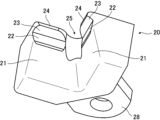
- FIG. 3 is a perspective view of the contact member according to the first embodiment of the present invention, and is a view of the contact member as seen from below.
- FIG. 4 is a plan view of the contact member according to the first embodiment of the invention.
- FIG. 5 is a side view of the contact member according to the first embodiment of the invention.
- FIG. 6 is a bottom view of the contact member according to the first embodiment of the invention.
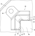
- FIG. 7 is a diagram showing the arrangement position of the contact member with respect to the mask member.
- FIG. 8 is an enlarged view of the periphery of the contact member in FIG. 7.
- FIG. FIG. 9 is a partial cross-sectional view showing the configuration of the urging device according to the first embodiment of the invention.
- 10A and 10B are diagrams showing a procedure for positioning the substrate by the contact member according to the first embodiment of the present invention (No. 1).
- FIG. 11 is a diagram showing the procedure for positioning the substrate by the contact member according to the first embodiment of the present invention (No. 2).
- 12A and 12B are diagrams showing the procedure for positioning the substrate by the contact member according to the first embodiment of the present invention (No. 3).
- FIG. 13 is a diagram showing the procedure for positioning the substrate by the contact member according to the first embodiment of the present invention (No. 4).
- FIG. 14 is a diagram showing the arrangement position of the contact member with respect to the mask member in the second embodiment of the present invention.
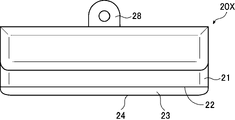
- FIG. 15 is a bottom view of the contact member according to the second embodiment of the invention.
- FIG. 16 is a bottom view of the contact member according to the third embodiment of the invention.
- a substrate holding device is a substrate holding device that positions and holds a substrate on which a thin film is formed on one main surface, and has an opening that defines a film forming region in the main surface.
- a mask member arranged at a position where the opening faces the main surface in a first direction; an urging device that urges the substrate toward the mask member along the first direction; a contact member integrated with the mask member and in contact with the outer edge of the substrate, the contact member moving in a second direction intersecting the first direction as it approaches the mask member in the first direction; an inclined surface inclined toward the inner side of the mask member in the direction; an extension surface located closer to the mask member than the inclined surface in the first direction and extending along the first direction; a contact surface located closer to the mask member than the extending surface in the first direction and in contact with the outer edge of the substrate in the first direction, wherein the substrate is biased by the biaser.
- the contact surface is moved to the outer edge portion of the substrate.
- the substrate is positioned by bringing it into contact with the substrate.
- the Z direction corresponds to the first direction of this embodiment and coincides with the thickness direction of the mask member 10 described later.
- the X and Y directions correspond to the second direction of this embodiment, are directions that cross (perpendicular to) the Z direction, and are horizontal directions when the Z direction is the vertical direction.
- "when viewed in plan view” means when viewed from the Z direction.
- the substrate B is a glass plate having a polygonal, more specifically rectangular, shape when viewed from above, and has main surfaces at both ends in the thickness direction of the substrate B.
- a thin film (conductive film) is formed on one main surface of the substrate B.
- film formation surface Sa the main surface on which the thin film is formed
- back surface Sb the other main surface located opposite to film formation surface Sa
- the film formation surface Sa is a flat surface, and the film formation surface Sa side of the outer edge of the substrate B is chamfered. That is, the outer edge portion of the substrate B has an outer edge surface Sc that is continuous with the film formation surface Sa and that is inclined with respect to the film formation surface Sa.
- the outer edge portion of the substrate B means the side end surface (peripheral surface) of the substrate B and its peripheral portion. Further, the four corners of the outer edge of the substrate B may each have a square shape or a rounded R shape.
- a basic configuration of a substrate holding device (hereinafter referred to as substrate holding device 1) according to the first embodiment will be described with reference to FIGS.
- the substrate holding apparatus 1 is used to manufacture a substrate with a conductive film, positions a substrate B in each of the XYZ directions during film formation, and holds the substrate B in the positioned state during film formation.
- the substrate holding device 1 has one mask member 10, a plurality of contact members 20, a plurality of biasers 30, and a base unit 40, as shown in FIG.
- the mask member 10, the contact member 20, the biaser 30, and the base unit 40 are arranged side by side in this order in the Z direction.
- the substrate holding device 1 holds the substrate B by sandwiching the substrate B between the mask member 10 and the biaser 30 in the Z direction. A substrate B is sandwiched between the mask member 10 and the biaser 30 in the Z direction.
- the substrate holding device 1 also includes a posture changing mechanism (not shown) that changes the posture of the substrate holding device 1 holding the substrate B.
- a posture changing mechanism (not shown) that changes the posture of the substrate holding device 1 holding the substrate B.
- the attitude change mechanism By the operation of the attitude change mechanism, the direction in which the above-described members constituting the substrate holding device 1 are arranged, that is, the Z direction is switched between the vertical direction and the cross direction.
- the intersecting direction is a direction intersecting with the vertical direction, such as a horizontal direction or a direction inclined with respect to both the vertical direction and the horizontal direction.
- the mask member 10 is made of a metal disk and has a square opening 12 in the central portion.
- the opening 12 is a through hole that defines a film formation region in the film formation surface Sa.
- the mask member 10 is arranged at a position where the opening 12 faces the film formation surface Sa in the Z direction. Also, the size of the opening 12 is slightly smaller than the size of the substrate B when viewed from above.
- a plurality of contact members 20 constitute the contact members of this embodiment.
- the number of contact members 20 is the same as the corners of the outer edge of the substrate B, that is, four contact members 20 .
- each of the plurality of contact members 20 contacts the outer edge of the substrate B.
- the plurality of contact members 20 are integrated with the mask member 10, and more specifically, are fixed to the surface of the mask member 10 facing the substrate B (hereinafter referred to as the bottom surface). The structure of the contact member 20 will be described later in detail.
- the plurality of urging devices 30 respectively urge the substrate B in the Z direction, and more specifically, urge the substrate B toward the mask member 10 while being in contact with the rear surface Sb of the substrate B.
- the same number of biasers 30 as the corners of the outer edge of the substrate B that is, four biasers 30 are provided.
- Each urging device 30 is arranged at a position that overlaps the edge portion of the opening 12 in the mask member 10 with the periphery of the corner in the Z direction. The configuration of the biaser 30 will be described later in detail.
- the base unit 40 forms the bottom of the substrate holding device 1 and supports a fixing base 42 for fixing the proximal end of the urging device 30 , a housing 44 located closer to the mask member 10 than the fixing base 42 , and the mask member 10 . It has a support arm 46 and a movable table 48 to which the base end of the support arm 46 is fixed. An elevator 50 is provided between the fixed table 42 and the movable table 48 in the Z direction.
- the elevator 50 is driven by an air cylinder (not shown) to move up and down, and as the elevator 50 moves up and down, the movable table 48 moves relative to the fixed table 42 in the Z direction. Along with this, the support arm 46 and the mask member 10 supported by the support arm 46 move in the same direction as the movable table 48 . As a result, the mask member 10 and the plurality of contact members 20 move relative to the substrate B placed on the tip of the biaser 30, and more specifically, move closer to or away from the substrate B. or
- the position, posture, etc. of the contact member 20 described below are those in a state where the contact member 20 is fixed to the mask member 10, unless otherwise specified. Further, hereinafter, for convenience of explanation, the side where the mask member 10 is positioned when viewed from the contact member 20 is called “upper side”, and the opposite side is called “lower side”.
- the contact member 20 is a block-shaped resin molding molded into the shape shown in FIGS.
- the contact member 20 can be made of various materials, but from the standpoint of moldability, the materials that make up the contact member 20 are, for example, polyetheretherketone (PEEK), polyimide, and polybenzimidazole (PBI).
- a resin material such as a resin, a fluororesin, a fluororubber, or an elastomer material may be used.
- PEEK polyetheretherketone
- polyimide polyimide
- fluororubber are more preferable
- polyetheretherketone (PEEK) is particularly preferable.
- elastomer materials include ester-based, amide-based, and olefin-based materials.
- the contact member 20 has an L-shaped bent shape when viewed from above.
- the contact member 20 has an inner wall surface and an outer wall surface, and contacts the substrate B at the inner wall surface.
- the inner wall surface of the contact member 20 is divided into two regions that intersect each other at the bend. The two regions are surfaces substantially orthogonal to each other, one region extending along the X direction and the other region extending along the Y direction.
- Each region has an inclined surface 21, an extending surface 22, an abutment surface 23 and a top surface 24 from the lower side of the contact member 20, as shown in FIGS.
- the inclined surface 21 is a surface that is inclined toward the inside of the mask member 10 in the X or Y direction, which is a direction intersecting the Z direction, as it approaches the mask member 10 in the Z direction (that is, as it goes upward).
- the inside of the mask member 10 is the side facing the center of the opening 12 .
- the inclination angle of the inclined surface 21 with respect to the Z direction is preferably 0° or more and 30° or less in order to position the substrate B by the procedure described later, and is preferably 10° or more and 20° or less. It is more preferable to have Here, it is preferably 0° or more, more preferably 10° or more, and preferably 30° or less, more preferably 20° or less.
- the extending surface 22 is a surface that is continuous with the inclined surface 21 above the inclined surface 21 in the Z direction (that is, on the mask member 10 side) and extends along the Z direction.
- the length of the extension surface 22 in the Z direction is not particularly limited, it is preferably set to a suitable length for positioning the substrate B based on the thickness of the substrate B. Specifically, when the thickness of the substrate B is T (MM), the length of the extension surface 22 in the Z direction is preferably 0.2T or more, more preferably 0.5T or more. .
- the contact surface 23 is continuous with the extension surface 22 above the extension surface 22 (that is, on the mask member 10 side) in the Z direction, and the outer edge of the substrate B in the Z direction when positioning the substrate B, more specifically, the outer edge. This is the surface that abuts on the surface Sc.
- the contact surface 23 is inclined toward the inside of the mask member 10 in the X or Y direction as it approaches the mask member 10 in the Z direction. be. That is, the inclination angle of the contact surface 23 with respect to the Z direction is substantially the same as the inclination angle of the outer edge surface Sc with respect to the thickness direction of the substrate B (that is, the Z direction).
- substantially the same does not mean that the values are exactly the same, but means that design errors are allowed. Specifically, it means that the difference between the inclination angle of the contact surface 23 and the inclination angle of the outer edge surface Sc is within ⁇ 10%.
- the top surface 24 forms the upper end of the inner wall surface of the contact member 20, is continuous with the contact surface 23 above the contact surface 23 (on the mask member 10 side) in the Z direction, and extends along the Z direction. It is the exposed side.
- a recess 25 is provided in the bent portion of the contact member 20, that is, in the portion where two regions intersect on the inner wall surface.
- the recessed portion 25 is formed toward the outside of the contact member 20 (the side away from the opening 12) in the X and Y directions, and the inner wall surface of the contact member 20 curves toward the outside of the contact member 20. It is formed by
- the concave portion 25 is formed in a substantially semicircular shape in plan view, and its curvature is smaller than the curvature of the corner of the substrate B when it is rounded. Since the concave portion 25 is provided in the bent portion of the contact member 20, it is possible to prevent foreign substances such as dirt and dust from accumulating in the bent portion.
- extension surfaces 22 of the two areas on the inner wall surface of the contact member 20 are arranged with the recess 25 interposed therebetween.
- contact surfaces 23 of the two regions are aligned with the recess 25 interposed therebetween, and the top surfaces 24 of the two regions are aligned with the recess 25 interposed therebetween.
- a tongue-shaped portion 28 protrudes outward from the outer wall surface of the contact member 20 .
- a hole is formed in the tongue-like portion 28 and is positioned with respect to the mask member 10 by bolting or the like and fixed to the bottom surface of the mask member 10 .
- the fixed position of the contact member 20 is not particularly limited, and may be any fixed position as long as the contact member 20 can be fixed so that the contact member 20 is preferably in contact with the substrate B.
- the contact members 20 are fixed along the edges of the openings 12 in the mask member 10. Specifically, as shown in FIG. A contact member 20 is fixed along the wall surface. As a result, when the substrate B is positioned, the plurality of (specifically, four) contact members 20 fixed to the mask member 10 are brought into contact with the corners of the outer edge of the substrate B. Become.
- the contact surface 23 and the top surface 24 are located inside the edge of the opening 12 (indicated by broken lines in FIG. 8). It is in.
- the dimension of the edge of the opening 12 is smaller than the dimension of the outer edge of the substrate B, and the extension surface 22 is located outside the outer edge of the substrate B when the substrate B is positioned with respect to the mask member 10 .
- the urging device 30 is composed of a main body portion 31 extending in the Z direction and a spring body 32 attached to the main body portion 31. It is in contact with the rear surface Sb, and the spring body 32 applies an elastic force to the main body 31 to press the front end of the main body 31 against the rear surface Sb.
- the main body portion 31 is configured by inserting a core rod portion 33 standing vertically from a fixed base 42 of the base unit 40 into a cylindrical portion 34 .
- the cylindrical portion 34 is supported by the core rod portion 33 so as to be movable in the Z direction with respect to the core rod portion 33 .
- the tip of the tubular portion 34 that is, the end on the side of the mask member 10, is closed to form a closed end.
- the spring body 32 is an elastic body, more specifically a coil spring, for example, and is accommodated in the cylindrical portion 34 and arranged between the core rod portion 33 and the cylindrical portion 34 . That is, in the first embodiment, the spring body 32 is provided individually for each urging device 30 , in other words, it is provided for each urging device 30 .
- the spring body 32 is preferably set to have a spring force suitable for stably holding the substrate B while being urged by the urging device 30. It is preferable to adjust the spring constant and the pressing amount so that the force corresponds to about 5 times or more and 10 times or less of .
- each urging device 30 one end of the spring body 32 is fixed to the inner wall surface of the tubular portion 34 and the other end of the spring body 32 is fixed to the core rod portion 33 . Accordingly, when the cylindrical portion 34 moves in the Z direction with respect to the core rod portion 33, the spring body 32 expands and contracts accordingly. Then, when the cylindrical portion 34 moves toward the fixing table 42 side (lower side) in the Z direction, the spring body 32 contracts to generate an elastic force, which acts on the cylindrical portion 34 . At this time, if the substrate B is placed on the projection 35, the apex of the projection 35 receives the elastic force of the spring body 32 and is pressed against the rear surface Sb of the substrate B. As shown in FIG.
- each of the plurality (specifically, four) biasers 30 is arranged at the same position as the corner portion of the opening 12 of the mask member 10 in the XY directions. More specifically, each biaser 30 is arranged to overlap at least a portion of the inner wall surface of the contact member 20 in the Z direction. As a result, each urging device 30 is in contact with the back surface Sb of the substrate B at each of the corners of the outer edge of the substrate B and urges the substrate B toward the mask member 10 .
- the substrate B comes into point contact with the protrusion 35 provided at the tip of the biaser 30 at the peripheral position of the corner, and is biased toward the mask member 10 by the biaser 30 .
- the board B can be held in a well-balanced manner by suppressing rattling of the board.
- the contact between the urging device 30 and the substrate B is point contact, the contact area with the substrate B can be made as small as possible. If the urging device 30 is in surface contact with the rear surface Sb of the substrate B, the substrate B may rattle if the contact surface of the urging device 30 is inclined with respect to the rear surface Sb. Since it is a point contact, the occurrence of such backlash can be suppressed.
- the body portion 31 and the spring body 32 that constitute the urging device 30 are arranged at a position farther from the film formation surface Sa than the rear surface Sb of the substrate B in the Z direction.
- the Z direction is set to the vertical direction, and the substrate B is gripped by a robot arm (not shown).
- the robot arm conveys the gripped substrate B to a position above the plurality of biasers 30 and places the four corner portions of the substrate B on the tips of the plurality of biasers 30 .
- the mask member 10 is at the farthest position (hereinafter referred to as the upper position) from the fixed table 42 in the Z direction due to the operation of the elevator 50 .
- the elevator 50 descends and the movable table 48 moves downward. Accordingly, the mask member 10 descends, and as a result, the substrate B urged by the plurality of urging devices 30 and the mask member 10 come closer to each other in the Z direction.
- each of the plurality of contact members 20 fixed to the bottom surface of the mask member 10 soon comes to be adjacent to the outer edge of the substrate B, as shown in FIG.
- the outer edge surface Sc of the substrate B will be the inclined surface 21 of the contact member 20 as shown in FIG. abut.
- the inclined surface 21 of one of the two contact members 20 (hereinafter referred to as a pair of contact members 20) positioned on the diagonal line of the opening 12 corresponds to the outer edge surface Sc of the substrate B. abuts.
- the inner wall surface of the contact member 20 that contacts the outer edge of the substrate B has two inclined surfaces 21 intersecting each other, but one inclined surface 21 may contact the outer edge surface Sc. Alternatively, both inclined surfaces 21 may abut against the outer edge surface Sc.
- the outer edge surface Sc in contact with the inclined surface 21 slides on the inclined surface 21 as shown in FIG. Thereby, the outer edge of the substrate B is guided upward (that is, toward the contact surface 23 ) along the inclined surface 21 . At this time, if the portion of the outer edge of the substrate B that is in contact with the inclined surface 21 is displaced outward from the normal position, that portion will be pushed by the inclined surface 21 in the X or Y direction to form the mask member. Move towards the inside of 10.
- the extending surface 22 of the contact member 20 whose inclined surface 21 contacts the outer edge surface Sc of the substrate B contacts the side end surface of the substrate B.
- the extended surface 22 of the other contact member 20 may or may not come into contact with the side end surface of the substrate B. As shown in FIG.
- the extension surface 22 in contact with the side end surface of the substrate B descends along the side end surface. move almost vertically to the As the mask member 10 is further lowered, the outer edge of the substrate B contacts the contact surface 23 of the contact member 20 in the Z direction as shown in FIG.
- the inner wall surface of the contact member 20 has two contact surfaces 23 that intersect with each other via the recess 25, but one of the contact surfaces 23 may contact the outer edge surface Sc, or , both of the contact surfaces 23 may contact the outer edge surface Sc.
- the substrate B is positioned in the XY directions. That is, in the first embodiment, the substrate B is urged toward the mask member 10 by the urging device 30, and the urged substrate B and the mask member 10 are brought closer to each other in the Z direction.
- the outer edge of the substrate B comes into contact with the inclined surface 21 of the contact member 20 , the outer edge of the substrate B is guided along the inclined surface 21 toward the contact surface 23 of the contact member 20 .
- the substrate B is displaced from the normal arrangement position in the XY directions, the substrate B is pushed inwardly of the mask member 10 by the inclined surface 21 and the position of the substrate B is corrected.
- the substrate B is positioned such that the film formation region in the film formation surface Sa is correctly exposed through the opening 12 .
- contact members 20 are provided in the first embodiment, at least two contact members 20 are preferably in contact with the outer edge of the substrate B from the viewpoint of holding the substrate B stably. Preferably, three or more contact members 20 are in contact, and most preferably all four contact members 20 are in contact.
- the substrate B is sandwiched between the contact member 20 and the urging device 30 in the Z direction, and pressed against the mask member 10 by the urging force (elastic force) of the urging device 30 .
- the distance between the mask member 10 and the substrate B in the Z direction is the distance corresponding to the length from the contact surface 23 to the mask member 10, that is, is an interval of constant size. Therefore, even if there is a variation in the thickness of the substrate B, the above spacing is not affected.
- the substrate B can be positioned so that the distance between the substrate B and the mask member 10 is a predetermined value in the Z direction. More specifically, since the contact member 20 and the mask member 10 are integrated, the outer edge portion of the substrate B is brought into contact with the contact surface 23 biased toward the mask member 10 by the biaser 30, thereby facilitating the Z direction. , the position of the substrate B with respect to the mask member 10 is determined. Thereby, after that, the distance between the film formation surface Sa of the substrate B and the mask member 10 is kept constant. Note that the distance between the substrate B and the mask member 10 can be adjusted by interposing a shim spacer (not shown) between the mask member 10 and the contact member 20 .
- the substrate B sandwiched between the contact member 20 and the urging device 30 is stably held at the position after positioning by the urging force of the urging device 30 . Further, even when the posture of the substrate holding device 1 is changed for film formation and the substrate B stands up from the horizontal posture, the holding state of the substrate B is favorably maintained by the urging force of the urging device 30 .
- the corner portion of the outer edge of the substrate B enters the concave portion 25 of the contact member 20 and is separated from the inner wall surface of the contact member 20 (Fig. 8). According to such a configuration, it is possible to prevent the corner portion of the outer edge of the substrate B from contacting and rubbing against the contact member 20 .
- the substrate B is positioned and held in each of the XYZ directions using the substrate holding device 1 of the present embodiment. Specifically, the Z direction is set to the vertical direction, and the substrate B is picked up by a robot arm (not shown) when the mask member 10 is in the upper position. After that, the substrate B is inserted into the space between the mask member 10 and the plurality of biasers 30 from the side of the substrate holding device 1 and placed on the tip of each biaser 30 . As a result, the substrate B is biased toward the mask member 10 by the plurality of biasers 30 in the Z direction.
- the mask member 10 is lowered by the elevator 50, and the substrate B and the mask member 10 urged by the urging device 30 are brought close to each other in the Z direction.
- the outer edge of the substrate B is brought into contact with the inclined surface 21 of the contact member 20 and guided along the inclined surface 21 toward the contact surface 23 of the contact member 20 .
- the contact surface 23 is brought into contact with the outer edge portion of the substrate B, more specifically, the outer edge surface Sc.
- the substrate B is positioned in the XY directions so that the film formation region in the film formation surface Sa of the substrate B is correctly exposed through the openings 12 of the mask member 10 .
- the spring bodies 32 of each urging device 30 contract to generate elastic force. Due to the elastic force, the substrate B is sandwiched between the contact member 20 and the urging device 30 and pressed against the mask member 10 side. Through the steps described above, the substrate B is positioned in the XYZ directions, and after that, the substrate B is held at the positioned position.
- the posture of the substrate holding device 1 is changed by the posture changing mechanism so that the Z direction is tilted with respect to the vertical direction.
- the film formation area exposed through the opening 12 on the film formation surface Sa of the substrate B faces a target (not shown).
- a conductive film is formed in the film formation region by a dry film formation method.
- a dry film-forming method known film-forming methods such as sputtering methods such as magnetron sputtering method and ion beam sputtering method, CVD (Chemical Vapor Deposition) method, and vacuum deposition method can be used.
- the contact member 20 When using the film forming method described above, it is preferable to use a material that does not release gas components under the vacuum atmosphere in the film forming container as the material that constitutes the contact member 20 of the substrate holding device 1 . Further, since the substrate B may be hot in the film forming apparatus, it is preferable that the contact member 20 have chemical and physical heat resistance up to at least about 150.degree.
- the substrate holding device 1 may be rotated during film formation.
- the extended surface 22 of the contact member 20 can cope with the centrifugal force generated by the rotation of the substrate holding device 1 .
- the method for manufacturing a substrate with a conductive film described above is used for manufacturing reflective mask blanks (hereinafter referred to as EUV mask blanks) for EUV (EXTREME ULTRAVIOLET) lithography used in semiconductor manufacturing, etc., or functions for EUV mask blanks. It is effective for manufacturing a substrate with a film.
- each of the plurality of contact members 20 has an L-shaped bent shape in plan view, and is fixed near the corner of the edge of the opening 12 in the mask member 10 . Further, in the first embodiment, when the substrate holding device 1 holds the substrate B, each contact member 20 contacts the corner portion of the outer edge of the substrate B. As shown in FIG. However, a second embodiment different from this configuration is conceivable. In the following, differences of the second embodiment from the first embodiment will be mainly described with reference to FIGS. 14 and 15. FIG.
- FIG. 14 and 15 are explanatory diagrams of the second embodiment, wherein FIG. 14 is a diagram corresponding to FIG. 7 and FIG. 15 is a diagram corresponding to FIG. 14 and 15 that are common to the first embodiment are given the same reference numerals as in the first embodiment.
- each of the four contact members 20X has a shape extending linearly in plan view, and is fixed to the central portion of each side forming the edge of the opening 12. ing.
- the inner wall surface of each contact member 20X has an inclined surface 21, an extending surface 22, an abutting surface 23 and a top surface 24, as shown in FIG.
- the shape of each surface is the same shape as in the first embodiment.
- the substrate holding device 1 holds the substrate B
- at least one of the four contact members 20X contacts the outer edge of the substrate B at the central portion of the side forming the outer edge of the substrate B.
- the same effects as in the first embodiment can be obtained. That is, even when the contact member 20X according to the second embodiment is used, the substrate B is positioned so that the film formation region in the film formation surface Sa is correctly exposed, and the distance between the substrate B and the mask member 10 is can be kept constant.
- two or more contact members 20X among the four contact members 20X are in contact with the substrate B, and in particular, it is preferable to contact the central portions of the opposite sides of the outer edge of the substrate B. Moreover, from the viewpoint of holding the substrate B more stably, it is more preferable that three or more contact members 20X contact the substrate B, and it is particularly preferable that all four contact members 20X contact the substrate B.
- the concave portion 25 is provided at the bent portion of the inner wall surface of each contact member 20 , and the concave portion 25 is formed by curving the inner wall surface toward the outside of the contact member 20 .
- a third embodiment is conceivable in which the shape of the recess is different from the shape described above. In the following, with reference to FIG. 16, the points of the third embodiment that are different from the first embodiment will be mainly described.
- FIG. 16 is an explanatory diagram of the third embodiment and corresponds to FIG. 6. Of the parts of the contact member shown in FIG. The same reference numerals as in the first embodiment are attached.
- a contact member 20Y according to the third embodiment has an L shape when viewed from above as shown in FIG. Further, the contact member 20Y is formed with a slit-shaped concave portion 26 formed in a bent portion. That is, the contact member 20Y is divided into two pieces (hereinafter referred to as contact member pieces 27) by the recess 26, which is a slit. In addition, in the example shown in FIG. 16, the two contact member pieces 27 are separated from each other, but a part of them may be connected.
- the two contact member pieces 27 are arranged at positions intersecting (more specifically, perpendicular to each other) via the recess 26, and the inner wall surface of each contact member piece 27 is composed of an inclined surface 21, an extending surface 22, an abutting surface 23, and a contact surface 23. It has a top surface 24 .
- the shape of each surface is the same shape as in the first embodiment.
- the concave portion 26 is provided, dirt and foreign matter such as dust can be discharged from the concave portion 26 at the corner portion of the contact member 20Y. Further, when the substrate B is held by the substrate holding device 1 , the corner portion of the outer edge of the substrate B enters the concave portion 26 . Since the concave portion 26 is a slit as described above, it is possible to prevent the corner portion of the outer edge portion of the substrate B from contacting and rubbing against the contact member 20Y.
- the contact surface 23 provided on the inner wall surface of each of the contact members 20, 20X, and 20Y is a surface perpendicular to the extension surface 22, that is, a horizontal surface, from the viewpoint of good contact with the outer edge surface Sc of the substrate B. Good to have.
- the urging device 30 may be composed of, for example, a leaf spring or the like, and may come into surface contact with the rear surface Sb of the substrate B. However, as described above, from the viewpoint of urging in a well-balanced manner, it is more preferable for the urging device 30 to make point contact with the rear surface Sb.
- the contact members 20, 20X, and 20Y may be configured by the same member as the mask member 10 instead of being a member separate from the mask member 10. That is, the contact members 20, 20X, 20Y and the mask member 10 may be integrally molded as one piece.
- the present invention can also be applied to a configuration in which the mask member 10 is fixed and the substrate B is movable, that is, a configuration in which the substrate B is moved with respect to the mask member 10.
- Reference Signs List 1 substrate holding device 10 mask member 12 openings 20, 20X, 20Y contact member 21 inclined surface 22 extension surface 23 contact surface 24 top surface 25, 26 recess 27 contact member piece 28 tongue-shaped portion 30 biaser 31 body portion 32 Spring body (elastic body) 33 Core rod portion 34 Cylindrical portion 35 Projection 40 Base unit 42 Fixed base 44 Housing 46 Support arm 48 Movable base 50 Elevator B Substrate Sa Film formation surface (one main surface) Sb back surface (other main surface) Sc Outer surface
Landscapes
- Chemical & Material Sciences (AREA)
- Chemical Kinetics & Catalysis (AREA)
- Engineering & Computer Science (AREA)
- Materials Engineering (AREA)
- Mechanical Engineering (AREA)
- Metallurgy (AREA)
- Organic Chemistry (AREA)
- Physical Vapour Deposition (AREA)
- Container, Conveyance, Adherence, Positioning, Of Wafer (AREA)
Priority Applications (1)
| Application Number | Priority Date | Filing Date | Title |
|---|---|---|---|
| JP2023545456A JP7513215B2 (ja) | 2021-08-30 | 2022-08-19 | 基板保持装置、及び導電膜付き基板の製造方法 |
Applications Claiming Priority (2)
| Application Number | Priority Date | Filing Date | Title |
|---|---|---|---|
| JP2021-139521 | 2021-08-30 | ||
| JP2021139521 | 2021-08-30 |
Publications (1)
| Publication Number | Publication Date |
|---|---|
| WO2023032721A1 true WO2023032721A1 (ja) | 2023-03-09 |
Family
ID=85412512
Family Applications (1)
| Application Number | Title | Priority Date | Filing Date |
|---|---|---|---|
| PCT/JP2022/031468 Ceased WO2023032721A1 (ja) | 2021-08-30 | 2022-08-19 | 基板保持装置、及び導電膜付き基板の製造方法 |
Country Status (2)
| Country | Link |
|---|---|
| JP (1) | JP7513215B2 (https=) |
| WO (1) | WO2023032721A1 (https=) |
Citations (8)
| Publication number | Priority date | Publication date | Assignee | Title |
|---|---|---|---|---|
| JPH08313856A (ja) * | 1995-05-18 | 1996-11-29 | Dainippon Screen Mfg Co Ltd | 基板搬送装置 |
| JP2005088921A (ja) * | 2003-09-16 | 2005-04-07 | Dainippon Printing Co Ltd | 基板収納ケース |
| JP2006328518A (ja) * | 2005-05-30 | 2006-12-07 | Optrex Corp | スパッタ成膜装置 |
| JP2008235294A (ja) * | 2007-03-16 | 2008-10-02 | Shinon Denki Sangyo Kk | 半導体集積回路用トレー |
| JP2011214034A (ja) * | 2010-03-31 | 2011-10-27 | Seiko Epson Corp | スパッタ装置 |
| JP2015175865A (ja) * | 2014-03-13 | 2015-10-05 | セイコーエプソン株式会社 | 光学部品、光学部品の製造方法、電子機器、および移動体 |
| JP2016092025A (ja) * | 2014-10-29 | 2016-05-23 | 東レエンジニアリング株式会社 | 基板保持装置および方法ならびに基板検査装置 |
| JP2016519778A (ja) * | 2013-03-12 | 2016-07-07 | アプライド マテリアルズ インコーポレイテッドApplied Materials,Incorporated | 極端紫外線リソグラフィマスクブランク製造システムとそのための操作方法 |
-
2022
- 2022-08-19 JP JP2023545456A patent/JP7513215B2/ja active Active
- 2022-08-19 WO PCT/JP2022/031468 patent/WO2023032721A1/ja not_active Ceased
Patent Citations (8)
| Publication number | Priority date | Publication date | Assignee | Title |
|---|---|---|---|---|
| JPH08313856A (ja) * | 1995-05-18 | 1996-11-29 | Dainippon Screen Mfg Co Ltd | 基板搬送装置 |
| JP2005088921A (ja) * | 2003-09-16 | 2005-04-07 | Dainippon Printing Co Ltd | 基板収納ケース |
| JP2006328518A (ja) * | 2005-05-30 | 2006-12-07 | Optrex Corp | スパッタ成膜装置 |
| JP2008235294A (ja) * | 2007-03-16 | 2008-10-02 | Shinon Denki Sangyo Kk | 半導体集積回路用トレー |
| JP2011214034A (ja) * | 2010-03-31 | 2011-10-27 | Seiko Epson Corp | スパッタ装置 |
| JP2016519778A (ja) * | 2013-03-12 | 2016-07-07 | アプライド マテリアルズ インコーポレイテッドApplied Materials,Incorporated | 極端紫外線リソグラフィマスクブランク製造システムとそのための操作方法 |
| JP2015175865A (ja) * | 2014-03-13 | 2015-10-05 | セイコーエプソン株式会社 | 光学部品、光学部品の製造方法、電子機器、および移動体 |
| JP2016092025A (ja) * | 2014-10-29 | 2016-05-23 | 東レエンジニアリング株式会社 | 基板保持装置および方法ならびに基板検査装置 |
Also Published As
| Publication number | Publication date |
|---|---|
| JPWO2023032721A1 (https=) | 2023-03-09 |
| JP7513215B2 (ja) | 2024-07-09 |
Similar Documents
| Publication | Publication Date | Title |
|---|---|---|
| TW490733B (en) | Substrate holding apparatus and exposure apparatus including substrate-holding apparatus | |
| JP6224437B2 (ja) | 基板搬送装置 | |
| US20160243707A1 (en) | Conveying hand and lithography apparatus | |
| US10571807B2 (en) | Method and apparatus for aligning substrates on a substrate support unit | |
| WO2013186929A1 (ja) | マスク保護装置、露光装置、及びデバイス製造方法 | |
| JP6671993B2 (ja) | 基板受け渡し位置の教示方法及び基板処理システム | |
| JPWO2011074474A1 (ja) | 基板支持部材、基板搬送装置、基板搬送方法、露光装置及びデバイス製造方法 | |
| CN102782798A (zh) | 具有透镜旋转的光刻系统 | |
| CN107587104A (zh) | 真空成膜装置 | |
| JP2012255958A (ja) | マスク保護装置、露光装置、及びデバイス製造方法 | |
| JP6723332B2 (ja) | 6自由度インプリントヘッドモジュールを有するナノインプリントリソグラフィ | |
| TWI242634B (en) | Substrate holder, substrate processing apparatus, substrate inspection device and method of using the same | |
| JP6981513B2 (ja) | マスク保持装置、露光装置、マスク保持方法、及び露光方法 | |
| CN114999987A (zh) | 卡盘、基板保持装置、基板处理装置及物品的制造方法 | |
| JP4620365B2 (ja) | 支持ステージに対して基板を位置決めするアライメント装置および基板較正システム | |
| WO2023032721A1 (ja) | 基板保持装置、及び導電膜付き基板の製造方法 | |
| JP2009537966A (ja) | レチクル及び他の平面体用のチャック | |
| JP5140010B2 (ja) | 基板ホルダー | |
| JP6275632B2 (ja) | 常温接合装置及び常温接合方法 | |
| JP5354419B2 (ja) | 部品の同時整列装置 | |
| JP4248341B2 (ja) | 被照射物保持機構 | |
| JP7329996B2 (ja) | 基板保持装置 | |
| JP2016129165A (ja) | 荷電粒子ビーム描画装置 | |
| JP7221238B2 (ja) | 基板支持構造体と、これを含む真空蒸着装置及び蒸着方法 | |
| CN108893709B (zh) | 用于直写式真空蒸发系统的掩模-基片间距控制系统 |
Legal Events
| Date | Code | Title | Description |
|---|---|---|---|
| 121 | Ep: the epo has been informed by wipo that ep was designated in this application |
Ref document number: 22864305 Country of ref document: EP Kind code of ref document: A1 |
|
| WWE | Wipo information: entry into national phase |
Ref document number: 2023545456 Country of ref document: JP |
|
| WWE | Wipo information: entry into national phase |
Ref document number: 11202401057S Country of ref document: SG |
|
| NENP | Non-entry into the national phase |
Ref country code: DE |
|
| 122 | Ep: pct application non-entry in european phase |
Ref document number: 22864305 Country of ref document: EP Kind code of ref document: A1 |