WO2023027149A1 - Matériau de fil supraconducteur et bobine supraconductrice - Google Patents
Matériau de fil supraconducteur et bobine supraconductrice Download PDFInfo
- Publication number
- WO2023027149A1 WO2023027149A1 PCT/JP2022/032059 JP2022032059W WO2023027149A1 WO 2023027149 A1 WO2023027149 A1 WO 2023027149A1 JP 2022032059 W JP2022032059 W JP 2022032059W WO 2023027149 A1 WO2023027149 A1 WO 2023027149A1
- Authority
- WO
- WIPO (PCT)
- Prior art keywords
- layer
- superconducting
- stabilizing
- oxide superconducting
- thickness
- Prior art date
Links
- 239000000463 material Substances 0.000 title abstract description 19
- 230000000087 stabilizing effect Effects 0.000 claims abstract description 93
- 229910052751 metal Inorganic materials 0.000 claims abstract description 60
- 239000002184 metal Substances 0.000 claims abstract description 60
- 239000000758 substrate Substances 0.000 claims abstract description 47
- 239000010410 layer Substances 0.000 description 161
- 239000011241 protective layer Substances 0.000 description 16
- 239000010949 copper Substances 0.000 description 15
- 230000006866 deterioration Effects 0.000 description 14
- 229910052802 copper Inorganic materials 0.000 description 13
- RYGMFSIKBFXOCR-UHFFFAOYSA-N Copper Chemical compound [Cu] RYGMFSIKBFXOCR-UHFFFAOYSA-N 0.000 description 11
- -1 Zr 2 O 3 Chemical class 0.000 description 9
- 238000004804 winding Methods 0.000 description 9
- 238000009792 diffusion process Methods 0.000 description 7
- BQCADISMDOOEFD-UHFFFAOYSA-N Silver Chemical compound [Ag] BQCADISMDOOEFD-UHFFFAOYSA-N 0.000 description 6
- 230000008878 coupling Effects 0.000 description 6
- 238000010168 coupling process Methods 0.000 description 6
- 238000005859 coupling reaction Methods 0.000 description 6
- 150000002739 metals Chemical class 0.000 description 6
- 239000004332 silver Substances 0.000 description 6
- 229910000990 Ni alloy Inorganic materials 0.000 description 5
- 230000008859 change Effects 0.000 description 5
- 239000000470 constituent Substances 0.000 description 5
- 230000008602 contraction Effects 0.000 description 5
- 229910000856 hastalloy Inorganic materials 0.000 description 5
- 229910052709 silver Inorganic materials 0.000 description 5
- 230000006641 stabilisation Effects 0.000 description 5
- 238000011105 stabilization Methods 0.000 description 5
- 229910000838 Al alloy Inorganic materials 0.000 description 4
- IJGRMHOSHXDMSA-UHFFFAOYSA-N Atomic nitrogen Chemical compound N#N IJGRMHOSHXDMSA-UHFFFAOYSA-N 0.000 description 4
- 229910000881 Cu alloy Inorganic materials 0.000 description 4
- 229910052782 aluminium Inorganic materials 0.000 description 4
- XAGFODPZIPBFFR-UHFFFAOYSA-N aluminium Chemical compound [Al] XAGFODPZIPBFFR-UHFFFAOYSA-N 0.000 description 4
- 230000000052 comparative effect Effects 0.000 description 4
- 238000009713 electroplating Methods 0.000 description 4
- 230000004048 modification Effects 0.000 description 4
- 238000012986 modification Methods 0.000 description 4
- 239000002887 superconductor Substances 0.000 description 4
- 229910001297 Zn alloy Inorganic materials 0.000 description 3
- 229910045601 alloy Inorganic materials 0.000 description 3
- 239000000956 alloy Substances 0.000 description 3
- 229910000679 solder Inorganic materials 0.000 description 3
- 229910001316 Ag alloy Inorganic materials 0.000 description 2
- 229910018072 Al 2 O 3 Inorganic materials 0.000 description 2
- 229910001020 Au alloy Inorganic materials 0.000 description 2
- 229910052693 Europium Inorganic materials 0.000 description 2
- 229910052688 Gadolinium Inorganic materials 0.000 description 2
- 229910002609 Gd2Zr2O7 Inorganic materials 0.000 description 2
- 229910017493 Nd 2 O 3 Inorganic materials 0.000 description 2
- 229910052772 Samarium Inorganic materials 0.000 description 2
- 238000006243 chemical reaction Methods 0.000 description 2
- 238000001816 cooling Methods 0.000 description 2
- 238000010586 diagram Methods 0.000 description 2
- 230000000694 effects Effects 0.000 description 2
- 239000010931 gold Substances 0.000 description 2
- 238000007735 ion beam assisted deposition Methods 0.000 description 2
- 239000007788 liquid Substances 0.000 description 2
- 230000005415 magnetization Effects 0.000 description 2
- 229910052757 nitrogen Inorganic materials 0.000 description 2
- 238000007747 plating Methods 0.000 description 2
- 230000002265 prevention Effects 0.000 description 2
- 229910052718 tin Inorganic materials 0.000 description 2
- 229910052727 yttrium Inorganic materials 0.000 description 2
- 241000954177 Bangana ariza Species 0.000 description 1
- 229910052684 Cerium Inorganic materials 0.000 description 1
- 229910017518 Cu Zn Inorganic materials 0.000 description 1
- 229910002480 Cu-O Inorganic materials 0.000 description 1
- 229910017752 Cu-Zn Inorganic materials 0.000 description 1
- 229910002482 Cu–Ni Inorganic materials 0.000 description 1
- 229910017943 Cu—Zn Inorganic materials 0.000 description 1
- 229910052692 Dysprosium Inorganic materials 0.000 description 1
- 229910052691 Erbium Inorganic materials 0.000 description 1
- 229910052689 Holmium Inorganic materials 0.000 description 1
- 206010021143 Hypoxia Diseases 0.000 description 1
- 229910000846 In alloy Inorganic materials 0.000 description 1
- 229910052765 Lutetium Inorganic materials 0.000 description 1
- 229910052779 Neodymium Inorganic materials 0.000 description 1
- 229910052777 Praseodymium Inorganic materials 0.000 description 1
- 229910052581 Si3N4 Inorganic materials 0.000 description 1
- 229910001128 Sn alloy Inorganic materials 0.000 description 1
- 229910002367 SrTiO Inorganic materials 0.000 description 1
- 229910052771 Terbium Inorganic materials 0.000 description 1
- 229910052775 Thulium Inorganic materials 0.000 description 1
- 229910001080 W alloy Inorganic materials 0.000 description 1
- 229910052769 Ytterbium Inorganic materials 0.000 description 1
- PNEYBMLMFCGWSK-UHFFFAOYSA-N aluminium oxide Inorganic materials [O-2].[O-2].[O-2].[Al+3].[Al+3] PNEYBMLMFCGWSK-UHFFFAOYSA-N 0.000 description 1
- 230000004888 barrier function Effects 0.000 description 1
- 229910052797 bismuth Inorganic materials 0.000 description 1
- CETPSERCERDGAM-UHFFFAOYSA-N ceric oxide Chemical compound O=[Ce]=O CETPSERCERDGAM-UHFFFAOYSA-N 0.000 description 1
- 229910000422 cerium(IV) oxide Inorganic materials 0.000 description 1
- TVZPLCNGKSPOJA-UHFFFAOYSA-N copper zinc Chemical compound [Cu].[Zn] TVZPLCNGKSPOJA-UHFFFAOYSA-N 0.000 description 1
- 229910052593 corundum Inorganic materials 0.000 description 1
- 239000013078 crystal Substances 0.000 description 1
- NLQFUUYNQFMIJW-UHFFFAOYSA-N dysprosium(III) oxide Inorganic materials O=[Dy]O[Dy]=O NLQFUUYNQFMIJW-UHFFFAOYSA-N 0.000 description 1
- 239000003822 epoxy resin Substances 0.000 description 1
- VQCBHWLJZDBHOS-UHFFFAOYSA-N erbium(III) oxide Inorganic materials O=[Er]O[Er]=O VQCBHWLJZDBHOS-UHFFFAOYSA-N 0.000 description 1
- RSEIMSPAXMNYFJ-UHFFFAOYSA-N europium(III) oxide Inorganic materials O=[Eu]O[Eu]=O RSEIMSPAXMNYFJ-UHFFFAOYSA-N 0.000 description 1
- PCHJSUWPFVWCPO-UHFFFAOYSA-N gold Chemical compound [Au] PCHJSUWPFVWCPO-UHFFFAOYSA-N 0.000 description 1
- 229910052737 gold Inorganic materials 0.000 description 1
- 239000003353 gold alloy Substances 0.000 description 1
- JYTUFVYWTIKZGR-UHFFFAOYSA-N holmium oxide Inorganic materials [O][Ho]O[Ho][O] JYTUFVYWTIKZGR-UHFFFAOYSA-N 0.000 description 1
- 239000012535 impurity Substances 0.000 description 1
- 229910052738 indium Inorganic materials 0.000 description 1
- APFVFJFRJDLVQX-UHFFFAOYSA-N indium atom Chemical compound [In] APFVFJFRJDLVQX-UHFFFAOYSA-N 0.000 description 1
- 229910052746 lanthanum Inorganic materials 0.000 description 1
- MRELNEQAGSRDBK-UHFFFAOYSA-N lanthanum oxide Inorganic materials [O-2].[O-2].[O-2].[La+3].[La+3] MRELNEQAGSRDBK-UHFFFAOYSA-N 0.000 description 1
- 229910052745 lead Inorganic materials 0.000 description 1
- 229910044991 metal oxide Inorganic materials 0.000 description 1
- 150000004706 metal oxides Chemical class 0.000 description 1
- 238000000034 method Methods 0.000 description 1
- 230000003647 oxidation Effects 0.000 description 1
- 238000007254 oxidation reaction Methods 0.000 description 1
- KTUFCUMIWABKDW-UHFFFAOYSA-N oxo(oxolanthaniooxy)lanthanum Chemical compound O=[La]O[La]=O KTUFCUMIWABKDW-UHFFFAOYSA-N 0.000 description 1
- 235000012771 pancakes Nutrition 0.000 description 1
- 229920000647 polyepoxide Polymers 0.000 description 1
- 229910052761 rare earth metal Inorganic materials 0.000 description 1
- 229920005989 resin Polymers 0.000 description 1
- 239000011347 resin Substances 0.000 description 1
- 239000010935 stainless steel Substances 0.000 description 1
- 229910001220 stainless steel Inorganic materials 0.000 description 1
- 230000007704 transition Effects 0.000 description 1
- 229910001845 yogo sapphire Inorganic materials 0.000 description 1
- RUDFQVOCFDJEEF-UHFFFAOYSA-N yttrium(III) oxide Inorganic materials [O-2].[O-2].[O-2].[Y+3].[Y+3] RUDFQVOCFDJEEF-UHFFFAOYSA-N 0.000 description 1
Images


Classifications
-
- H—ELECTRICITY
- H01—ELECTRIC ELEMENTS
- H01B—CABLES; CONDUCTORS; INSULATORS; SELECTION OF MATERIALS FOR THEIR CONDUCTIVE, INSULATING OR DIELECTRIC PROPERTIES
- H01B12/00—Superconductive or hyperconductive conductors, cables, or transmission lines
- H01B12/02—Superconductive or hyperconductive conductors, cables, or transmission lines characterised by their form
- H01B12/06—Films or wires on bases or cores
-
- H—ELECTRICITY
- H01—ELECTRIC ELEMENTS
- H01F—MAGNETS; INDUCTANCES; TRANSFORMERS; SELECTION OF MATERIALS FOR THEIR MAGNETIC PROPERTIES
- H01F6/00—Superconducting magnets; Superconducting coils
- H01F6/06—Coils, e.g. winding, insulating, terminating or casing arrangements therefor
-
- Y—GENERAL TAGGING OF NEW TECHNOLOGICAL DEVELOPMENTS; GENERAL TAGGING OF CROSS-SECTIONAL TECHNOLOGIES SPANNING OVER SEVERAL SECTIONS OF THE IPC; TECHNICAL SUBJECTS COVERED BY FORMER USPC CROSS-REFERENCE ART COLLECTIONS [XRACs] AND DIGESTS
- Y02—TECHNOLOGIES OR APPLICATIONS FOR MITIGATION OR ADAPTATION AGAINST CLIMATE CHANGE
- Y02E—REDUCTION OF GREENHOUSE GAS [GHG] EMISSIONS, RELATED TO ENERGY GENERATION, TRANSMISSION OR DISTRIBUTION
- Y02E40/00—Technologies for an efficient electrical power generation, transmission or distribution
- Y02E40/60—Superconducting electric elements or equipment; Power systems integrating superconducting elements or equipment
Definitions
- the present invention relates to a superconducting wire and a superconducting coil.
- the superconducting wire described in Patent Document 1 includes a laminate in which a substrate, an intermediate layer, an oxide superconducting layer, and a protective layer are laminated, a stabilizing layer covering the laminate, and a metal formed on one surface of the stabilizing layer a tape;
- the metal tape is formed on the side of the laminate on which the oxide superconducting layer is formed, of the two sides of the stabilization layer.
- the substrate is made of Hastelloy (registered trademark), for example.
- the stabilization layer and metal tape are made of copper, for example.
- the shrinkage of the superconducting wire due to temperature changes may damage the oxide superconducting layer and reduce the superconducting properties.
- the superconducting wire when the superconducting wire is cooled to a temperature below the critical temperature (approximately 90 K or below in the case of a Y-based superconducting wire), the superconducting wire shrinks and deforms, and the substrate (Hastelloy (registered trademark)), the stabilizing layer and the metal Shear stress is applied to the oxide superconducting layer due to the difference in thermal expansion coefficient from the tape (both copper). This may damage the oxide superconducting layer and degrade the properties of the superconducting wire.
- the critical temperature approximately 90 K or below in the case of a Y-based superconducting wire
- the stabilizing layer and the metal Shear stress is applied to the oxide superconducting layer due to the difference in thermal expansion coefficient from the tape (both copper). This may damage the oxide superconducting layer and degrade the properties of the superconduct
- An object of one aspect of the present invention is to provide a superconducting wire and a superconducting coil whose superconducting properties are less likely to deteriorate due to temperature changes.
- a superconducting wire includes a superconducting laminate having a metal substrate and an oxide superconducting layer, a stabilizing portion formed to cover the superconducting laminate and having a thermal expansion coefficient larger than that of the metal substrate,
- the superconducting laminate has a first main surface on which the oxide superconducting layer is provided and a second main surface on which the metal substrate is provided, and
- the stabilizing portion has a first portion facing the first main surface and a second portion facing the second main surface, and the thickness of the second portion is equal to the thickness of the second main surface. Greater than the thickness of one part.
- the second portion of the stabilizing portion is thicker than the first portion, shear stress is less likely to act on the oxide superconducting layer even if the stabilizing portion shrinks due to temperature changes. Therefore, damage to the oxide superconducting layer can be suppressed. Therefore, deterioration of the superconducting properties of the superconducting wire can be suppressed.
- the difference between the thickness of the first portion and the thickness of the second portion may be greater than the thickness of the metal substrate.
- the stabilizing portion includes a first stabilizing layer surrounding the superconducting laminate and a second stabilizing layer formed of a metal tape and joined to a portion of the first stabilizing layer facing the second main surface. and a stabilization layer.
- a non-oriented region extending in the longitudinal direction of the oxide superconducting layer may be formed in the oxide superconducting layer.
- a superconducting coil according to another aspect of the present invention includes the superconducting wire, and the superconducting wire is wound so that the first portion is located radially inside the second portion.
- FIG. 1 is a cross-sectional view of an oxide superconducting wire according to a first embodiment
- FIG. 1 is a schematic diagram of a superconducting coil of a first embodiment
- FIG. 4 is a cross-sectional view of an oxide superconducting wire according to a second embodiment
- FIG. 4 is a cross-sectional view of an oxide superconducting wire according to a modification of the first embodiment
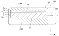
- FIG. 1 is a cross-sectional view of an oxide superconducting wire 10 of the first embodiment.
- FIG. 1 is a cross-sectional view orthogonal to the longitudinal direction of oxide superconducting wire 10 .
- the oxide superconducting wire 10 includes a superconducting laminate 5 and a stabilizing portion 6 .
- the oxide superconducting wire 10 is a specific example of "superconducting wire”.
- the superconducting laminate 5 includes a metal substrate 1 , an intermediate layer 2 , an oxide superconducting layer 3 and a protective layer 4 .
- a superconducting laminate 5 has a structure in which an oxide superconducting layer 3 and a protective layer 4 are formed on a metal substrate 1 with an intermediate layer 2 interposed therebetween. That is, superconducting laminate 5 has a configuration in which intermediate layer 2 , oxide superconducting layer 3 , and protective layer 4 are laminated in this order on one surface of tape-shaped metal substrate 1 .
- the oxide superconducting wire 10 is formed in a tape shape.
- the thickness direction of oxide superconducting wire 10 is referred to as thickness direction Y.
- the thickness direction Y is the direction in which the metal substrate 1, the intermediate layer 2, the oxide superconducting layer 3, and the protective layer 4 are laminated.
- the width direction of oxide superconducting wire 10 is referred to as width direction X.
- a width direction X is a direction orthogonal to the longitudinal direction and the thickness direction of oxide superconducting wire 10 .
- the metal substrate 1 is made of metal.
- the metal forming the metal substrate 1 include a nickel alloy such as Hastelloy (registered trademark); stainless steel; and an oriented Ni—W alloy in which a texture is introduced into a nickel alloy.
- the thickness of the metal substrate 1 may be appropriately adjusted depending on the purpose, and is in the range of 10 to 500 ⁇ m, for example.
- One surface of the metal substrate 1 (the surface on which the intermediate layer 2 is formed) is called a first surface 1a, and the surface opposite to the first surface 1a is called a second surface 1b.
- the intermediate layer 2 is provided between the metal substrate 1 and the oxide superconducting layer 3 .
- the intermediate layer 2 is formed on the first surface 1 a of the metal substrate 1 .
- the intermediate layer 2 may have a multi-layer structure, and may have, for example, a diffusion prevention layer, a bed layer, an orientation layer, a cap layer, etc. in order from the metal substrate 1 side to the oxide superconducting layer 3 side. These layers are not necessarily provided one by one, and some layers may be omitted, or two or more layers of the same kind may be repeatedly laminated. Note that intermediate layer 2 is not an essential component in oxide superconducting wire 10, and intermediate layer 2 may not be formed when metal substrate 1 itself has orientation.
- the anti-diffusion layer has a function of preventing some of the components of the metal substrate 1 from diffusing and entering the oxide superconducting layer 3 as impurities.
- the diffusion prevention layer is composed of, for example, Si3N4 , Al2O3 , GZO ( Gd2Zr2O7 ), or the like .
- the thickness of the anti-diffusion layer is, for example, 10-400 nm.
- a bed layer may be formed on the diffusion barrier layer.
- the bed layer is provided to reduce the reaction at the interface between metal substrate 1 and oxide superconducting layer 3 and to improve the orientation of layers formed on the bed layer.
- Examples of the bed layer material include Y2O3 , Er2O3 , CeO2 , Dy2O3 , Eu2O3 , Ho2O3 , La2O3 , and the like.
- the thickness of the bed layer is, for example, 10-100 nm.
- the alignment layer is formed of a material that is biaxially oriented to control the crystallographic orientation of the cap layer formed over the alignment layer.
- Materials for the alignment layer include, for example, Gd 2 Zr 2 O 7 , MgO, ZrO 2 —Y 2 O 3 (YSZ), SrTiO 3 , CeO 2 , Y 2 O 3 , Al 2 O 3 , Gd 2 O 3 , Metal oxides such as Zr 2 O 3 , Ho 2 O 3 and Nd 2 O 3 can be exemplified.
- the orientation layer is preferably formed by an IBAD (Ion-Beam-Assisted Deposition) method.
- the cap layer is formed on the surface of the orientation layer and is made of a material that allows crystal grains to self-orient in the in-plane direction.
- Materials for the cap layer include, for example, CeO 2 , Y 2 O 3 , Al 2 O 3 , Gd 2 O 3 , ZrO 2 , YSZ, Ho 2 O 3 , Nd 2 O 3 and LaMnO 3 .
- the thickness of the cap layer may range from 50 to 5000 nm.
- the oxide superconducting layer 3 is composed of an oxide superconductor.
- the oxide superconductor is not particularly limited, but for example, an RE-Ba-Cu-O-based oxide superconductor (REBCO-based oxide superconductor) represented by the general formula REBa 2 Cu 3 O X (RE123) can be mentioned. be done.
- the rare earth element RE includes one or more of Y, La, Ce, Pr, Nd, Sm, Eu, Gd, Tb, Dy, Ho, Er, Tm, Yb, and Lu. Among them, one of Y, Gd, Eu and Sm or a combination of two or more of these elements is preferable.
- X is 7-x (oxygen deficiency x: approximately 0 to 1).
- the thickness of the oxide superconducting layer 3 is, for example, within the range of 0.5-5 ⁇ m.
- the thickness of oxide superconducting layer 3 is preferably uniform in the longitudinal direction.
- Oxide superconducting layer 3 is formed on main surface 2a of intermediate layer 2 (the surface opposite to metal substrate 1).
- the protective layer 4 has functions such as bypassing an overcurrent that occurs at the time of an accident and suppressing chemical reactions that occur between the oxide superconducting layer 3 and a layer provided on the protective layer 4 .
- Examples of materials for the protective layer 4 include silver (Ag), copper (Cu), gold (Au), alloys of gold and silver, other silver alloys, copper alloys, and gold alloys.
- Protective layer 4 covers at least main surface 3a of oxide superconducting layer 3 (the surface opposite to intermediate layer 2 side). Although the thickness of the protective layer 4 is not particularly limited, it is in the range of 1 to 30 ⁇ m, for example.
- the superconducting laminate 5 has a first main surface 5a, side surfaces 5b and 5b, and a second main surface 5c.
- the first major surface 5 a is the major surface 4 a of the protective layer 4 .
- the first main surface 5a is the surface of the superconducting laminate 5 on which the oxide superconducting layer 3 is provided.
- Sides 5 b are the side of metal substrate 1 , the side of intermediate layer 2 , the side of oxide superconducting layer 3 , and the side of protective layer 4 .
- the second principal surface 5c is a surface opposite to the first principal surface 5a.
- the second main surface 5 c is the second surface 1 b of the metal substrate 1 .
- the second main surface 5c is the surface of the superconducting laminate 5 on which the metal substrate 1 is provided.
- the stabilizing portion 6 includes a first stabilizing layer 7 and a second stabilizing layer 8 .
- the stabilizing portion 6 functions as a bypass portion for commutating overcurrent generated when the oxide superconducting layer 3 transitions to the normal conducting state.
- the coefficient of thermal expansion of stabilizing portion 6 is greater than that of metal substrate 1 .
- the thermal expansion coefficient of Hastelloy (registered trademark) as the constituent material of the metal substrate 1 is 10.9 ⁇ 10 ⁇ 6 /° C.
- the thermal expansion coefficient of copper as the constituent material of the stabilizing portion 6 is 16.7. ⁇ 10 -6 /°C.
- the first stabilizing layer 7 covers the first main surface 5a, the side surfaces 5b, 5b and the second main surface 5c of the superconducting laminate 5. As shown in FIG. The first stabilizing layer 7 is integrally formed surrounding the superconducting laminate 5 . The first stabilizing layer 7 is formed from the first major surface 5a to the second major surface 5c. Examples of the constituent material of the first stabilizing layer 7 include metals such as copper, copper alloys (eg, Cu--Zn alloys, Cu--Ni alloys, etc.), aluminum, aluminum alloys, and silver. The thickness of the first stabilizing layer 7 is, for example, within the range of 10-500 ⁇ m. The first stabilizing layer 7 can be formed, for example, by plating (eg, electrolytic plating).
- the first stabilizing layer 7 has an upper portion 7A and a lower portion 7B.
- the upper portion 7A is the portion of the first stabilizing layer 7 facing the first major surface 5a.
- the upper portion 7A is the first portion 6A of the stabilizing portion 6 (the portion of the stabilizing portion 6 facing the first main surface 5a).
- the thickness of the upper portion 7A (first portion 6A) is referred to as T1.
- the lower portion 7B is the portion of the first stabilizing layer 7 facing the second main surface 5c.
- Superconducting laminate 5 and first stabilizing layer 7 constitute superconducting wire main body 11 .
- the second stabilizing layer 8 is composed of a metal tape.
- Metals constituting the metal tape include metals such as copper, copper alloys (eg, Cu--Zn alloys, Cu--Ni alloys, etc.), aluminum, aluminum alloys, and silver.
- the second stabilizing layer 8 is preferably a copper tape.
- thermal expansion coefficients of the metals used as constituent materials of the first stabilizing layer 7 and the second stabilizing layer 8 are shown below.
- the thermal expansion coefficient of Cu—Zn alloy is 19.1 ⁇ 10 ⁇ 6 /° C.
- the thermal expansion coefficient of Cu—Ni alloy is 13.8 ⁇ 10 ⁇ 6 /° C.
- the thermal expansion coefficient of aluminum is 23.8 ⁇ 10 ⁇ 6 /° C.
- the thermal expansion coefficient of Al- 6061 which is an example of an aluminum alloy, is 22.5 ⁇ 10 ⁇ 6 /° C.
- the thermal expansion coefficient of silver is 18.5 ⁇ 10 ⁇ 6 /° C. °C.
- the second stabilizing layer 8 is bonded to the lower surface of the first stabilizing layer 7 (outer surface of the lower portion 7B) with a bonding material 9 .
- materials forming the bonding material 9 include metals such as solder, Sn, Sn alloys, In (indium), and In alloys.
- solder include alloys such as Sn--Pb, Pb--Sn--Sb, Sn--Pb--Bi, Bi--Sn, Sn--Cu, Sn--Pb--Cu and Sn--Ag. .
- a portion of the stabilizing portion 6 facing the second main surface 5c is called a second portion 6B.
- the second portion 6B comprises a lower portion 7B of the first stabilizing layer 7, a bonding material 9 and a second stabilizing layer 8.
- the thickness of the second portion 6B is called T2.
- the thickness T2 is the sum of the thickness of the lower portion 7B, the thickness of the bonding material 9, and the thickness of the second stabilizing layer 8.
- the thickness T2 of the second portion 6B is greater than the thickness T1 of the first portion 6A (upper portion 7A). Since the thickness T2 is larger than the thickness T1, the shear stress caused by shrinkage of the stabilizing portion 6 due to temperature change is less likely to act on the oxide superconducting layer 3 . For example, the stabilizing portion 6 shrinks and deforms during cooling, but since the first portion 6A is thinner than the second portion 6B, shear stress is less likely to act on the oxide superconducting layer 3 .
- the difference (T2-T1) between the thickness T2 of the second portion 6B and the thickness T1 of the upper portion 7A (first portion 6A) is preferably larger than the thickness T3 of the metal substrate 1. Since this difference (T2 ⁇ T1) is larger than the thickness T3, the shear stress caused by shrinkage of the stabilizing portion 6 due to temperature change is less likely to act on the oxide superconducting layer 3 .
- FIG. 2 is a schematic diagram of the superconducting coil 20.
- superconducting coil 20 is formed of oxide superconducting wire 10 .
- Superconducting coil 20 is a multi-layer wound coil in which oxide superconducting wire 10 is laminated in the thickness direction and wound multiple times.
- the oxide superconducting wire 10 is wound around a winding axis C.
- the superconducting coil 20 is formed in an annular shape and is also called a pancake coil.
- a direction around the winding axis C as viewed from the winding axis C is called a circumferential direction of the superconducting coil 20 .
- a direction orthogonal to the winding axis C is called a radial direction of the superconducting coil 20 .
- the direction toward the winding axis C is called the radial inner side
- the direction away from the winding axis C is called the radial outer side.
- the oxide superconducting wire 10 is preferably wound around the winding axis C so that the metal substrate 1 faces radially outward and the oxide superconducting layer 3 faces radially inward. That is, oxide superconducting wire 10 is preferably wound around winding axis C such that oxide superconducting layer 3 is located radially inward of metal substrate 1 .
- the oxide superconducting layer 3 is pulled from the metal substrate by the Lorentz force acting in the radial direction of the superconducting coil 20 . pressed to 1. Therefore, it is possible to suppress the deterioration of the superconducting properties due to the oxide superconducting layer 3 being peeled off from the metal substrate 1 .
- the superconducting coil 20 may have a structure in which an insulating tape is wound around the oxide superconducting wire 10 .
- Superconducting coil 20 may be impregnated with resin such as epoxy resin.
- thickness T2 of second portion 6B of stabilizing portion 6 is greater than thickness T1 of first portion 6A (upper portion 7A).
- stabilizing portion 6 contracts. Since the thickness T2 is larger than the thickness T1, that is, the thickness T1 is smaller than the thickness T2, the shear force caused by the contraction of the first portion 6A is smaller than the shear force caused by the contraction of the second portion 6B. Since oxide superconducting layer 3 is formed closer to first portion 6A than second portion 6B, shear stress caused by shrinkage of stabilizing portion 6 is less likely to act on oxide superconducting layer 3 . Therefore, damage to oxide superconducting layer 3 can be suppressed. Therefore, deterioration of superconducting properties of oxide superconducting wire 10 can be suppressed.
- the second stabilizing layer 8 is formed on the outer surface of the upper portion 7A (first stabilizing layer 7 Assume an oxide superconducting wire bonded to the top surface of the In this oxide superconducting wire, the first portion of the stabilizing portion is thicker than the second portion. In this oxide superconducting wire, shear stress is likely to act on oxide superconducting layer 3 due to contraction of second stabilizing layer 8 due to temperature change. The shear stress tends to increase as the thickness of the second stabilizing layer 8 increases.
- FIG. 3 is a cross-sectional view of an oxide superconducting wire 110 of the second embodiment.
- the same reference numerals are attached to the common configuration with the first embodiment, and the description thereof is omitted.
- the oxide superconducting wire 110 includes a superconducting laminate 5 and a stabilizing portion 106 .
- Oxide superconducting wire 110 is a specific example of a “superconducting wire”.
- Stabilizing portion 106 is a layer integrally formed to cover superconducting laminate 5 .
- Stabilizing portion 106 covers first main surface 5 a , side surfaces 5 b and 5 b and second main surface 5 c of superconducting laminate 5 .
- Stabilizing portion 106 is formed to surround superconducting laminate 5 .
- Stabilizing portion 106 is formed from first main surface 5a to second main surface 5c.
- the coefficient of thermal expansion of stabilizing portion 106 is greater than that of metal substrate 1 .
- the constituent material of the stabilizing portion 106 include metals such as copper, copper alloys (eg, Cu--Zn alloys, Cu--Ni alloys, etc.), aluminum, aluminum alloys, and silver.
- the stabilizing portion 106 can be formed, for example, by plating (for example, electrolytic plating).
- a portion of the stabilizing portion 106 facing the first main surface 5a is called a first portion 106A.
- the thickness of the first portion 106A is called T11.
- a portion of the stabilizing portion 106 facing the second main surface 5c is referred to as a second portion 106B.
- the thickness of the second portion 106B is called T12.
- the thickness T12 of the second portion 106B is greater than the thickness T11 of the first portion 106A.
- Thickness T ⁇ b>12 is greater than thickness T ⁇ b>11 , so that shear stress caused by shrinkage of stabilizing portion 106 due to temperature change is less likely to act on oxide superconducting layer 3 .
- stabilizing portion 106 shrinks and deforms during cooling, but since first portion 106A is thinner than second portion 106B, shear stress is less likely to act on oxide superconducting layer 3 .
- the difference (T12-T11) between the thickness T12 of the second portion 106B and the thickness T11 of the first portion 106A is preferably larger than the thickness T3 of the metal substrate 1. Since this difference (T12 ⁇ T11) is larger than the thickness T3, the shear stress caused by shrinkage of the stabilizing portion 106 due to temperature change is less likely to act on the oxide superconducting layer 3 .
- thickness T12 of second portion 106B of stabilizing portion 106 is greater than thickness T11 of first portion 106A.
- Stabilizing portion 106 shrinks when oxide superconducting wire 110 is exposed to temperature changes. Since the thickness T12 is greater than the thickness T11, that is, the thickness T11 is less than the thickness T12, the shear force caused by the contraction of the first portion 106A is smaller than the shear force caused by the contraction of the second portion 106B. Since oxide superconducting layer 3 is formed closer to first portion 106A than second portion 106B, shear stress caused by shrinkage of stabilizing portion 106 is less likely to act on oxide superconducting layer 3 . Therefore, damage to oxide superconducting layer 3 can be suppressed. Therefore, deterioration of superconducting properties of oxide superconducting wire 110 can be suppressed.
- the present invention has been described above based on the preferred embodiments, the present invention is not limited to the above-described embodiments, and various modifications are possible without departing from the gist of the present invention.
- the oxide superconducting wire 10 shown in FIG. It may be joined directly to the first stabilizing layer 7 without any bonding.
- the second stabilizing layer 8 is bonded to the first stabilizing layer 7 by, for example, ultrasonic bonding, diffusion bonding, or the like.
- the structure of the superconducting laminate is not limited to the structure shown in FIG.
- the superconducting laminate may not have a protective layer.
- the superconducting laminate may contain layers other than the metal substrate, the intermediate layer, the oxide superconducting layer, and the protective layer.
- FIG. 4 is a cross-sectional view of an oxide superconducting wire 10 of a modification of the first embodiment.
- a non-oriented region (non-superconducting region) 32 is formed in the oxide superconducting layer 3 . That is, the oxide superconducting layer 3 has an oriented region (superconducting region) 31 and a non-oriented region 32 .
- the non-oriented region 32 may be formed by forming a groove in the metal substrate 1 or the intermediate layer 2 and providing the oxide superconducting layer 3 on the groove.
- Non-oriented regions 32 extend in the longitudinal direction of oxide superconducting layer 3 .
- a plurality of non-orientation regions 32 are arranged side by side in the width direction X.
- the non-oriented regions 32 do not have superconducting properties due to the disturbed orientation. Therefore, during use, it is difficult for current to flow through the non-oriented regions 32, and the oxide superconducting layer 3 is substantially divided in the width direction.
- the oxide superconducting layer 3 is thinned (multifilamentized). Therefore, the shielding current and magnetization loss of oxide superconducting wire 10 can be reduced, and deterioration of the properties of superconducting coil 20 can be suppressed.
- the stabilizing portion 6 (first portion 6A) is interposed, Coupling current may flow.
- the coupling current may degrade the properties of superconducting coil 20 .
- the first portion 6A of the stabilization portion 6 is thinner than the second portion 6B, the coupling current between the alignment regions 31 is reduced compared to when the first portion 6A is thicker than the second portion 6B. It becomes difficult to flow. Therefore, deterioration of the characteristics of the superconducting coil 20 due to the coupling current can be suppressed.
- the non-oriented regions 32 may be formed in the oxide superconducting layer 3 in the same manner as described above. That is, in oxide superconducting wire 110 , oxide superconducting layer 3 may have oriented regions 31 and non-oriented regions 32 . In this case also, the oxide superconducting layer 3 is thinned (multifilamentized) by the non-oriented regions 32, so that the shielding current and magnetization loss of the oxide superconducting wire 10 can be reduced, and the characteristics of the superconducting coil 20 can be improved. Decrease can be suppressed.
- the coupling current between the alignment regions 31 is reduced compared to the case where the first portion 106A is thicker than the second portion 106B. It becomes difficult to flow. Therefore, deterioration of the characteristics of the superconducting coil 20 due to the coupling current can be suppressed.
- Examples 1-3 A sample of the oxide superconducting wire 10 shown in FIG. 1 was produced as follows. An intermediate layer 2 was formed on one surface of a tape-shaped metal substrate 1 made of Hastelloy (registered trademark). The intermediate layer 2 has a structure in which an anti-diffusion layer, a bed layer, an orientation layer and a cap layer are laminated in this order. An oxide superconducting layer 3 made of GdBCO was formed on the intermediate layer 2 . A protective layer 4 made of Ag was formed on the oxide superconducting layer 3 . Thus, a superconducting laminate 5 was obtained.
- a first stabilizing layer 7 made of copper was formed on the outer surface of the superconducting laminate 5 by electroplating to obtain a superconducting wire main body 11 having a width of 4 mm.
- the second stabilizing layer 8, which is a copper tape, was joined to the lower surface of the first stabilizing layer 7 (the outer surface of the lower portion 7B) using solder as the joining material 9. As shown in FIG. Thus, a stabilizing portion 6 was formed.
- a sample of oxide superconducting wire 10 was placed in liquid nitrogen, and the critical current (Ic) was measured.
- a sample of the superconducting wire (that is, the superconducting laminate 5) before forming the stabilizing portion 6 was prepared, and the sample was placed in liquid nitrogen to measure the critical current (Ic0).
- the ratio (Ic/Ic0) of the critical current (Ic) of the oxide superconducting wire 10 and the critical current (Ic0) of the superconducting laminate 5 was 0.95 or more, it was determined that the superconducting properties did not deteriorate. .
- Ic/Ic0 was less than 0.95, it was determined that the superconducting properties were degraded.
- a case where the superconducting properties are not degraded is judged as "Pass”.
- a case where the superconducting property is degraded is defined as "failed”. Table 1 shows the results.
- Example 4 A sample of the oxide superconducting wire 110 shown in FIG. 3 was produced as follows. Stabilizing portion 106 made of copper was formed by electroplating on the outer surface of superconducting laminate 5 produced in the same manner as in Examples 1 to 3, and oxide superconducting wire 110 was obtained.
- Example 2 A sample of the oxide superconducting wire was produced according to Example 1, except that the second stabilizing layer 8 was bonded to the outer surface of the upper portion 7A of the first stabilizing layer 7 (upper surface of the first stabilizing layer 7). .
- the presence or absence of deterioration in superconducting properties was determined in the same manner as in Examples 1-3. Table 1 shows the results.
- Example 3 A sample of the oxide superconducting wire was produced according to Example 4, except that the first portion of the stabilizing portion was thicker than the second portion. For this sample, the presence or absence of deterioration in superconducting properties was determined in the same manner as in Examples 1-3. Table 1 shows the results.
Landscapes
- Engineering & Computer Science (AREA)
- Power Engineering (AREA)
- Superconductors And Manufacturing Methods Therefor (AREA)
Abstract
L'invention concerne un matériau de fil supraconducteur comprenant : un corps stratifié supraconducteur qui a un substrat métallique et une couche supraconductrice à oxyde ; et une partie de stabilisation qui est formée de manière à recouvrir le corps stratifié supraconducteur et qui a un coefficient de dilatation thermique plus grand que le substrat métallique. Le corps stratifié supraconducteur comprend : une première surface primaire qui est une surface sur le côté sur lequel la couche supraconductrice à oxyde est disposée ; et une seconde surface principale qui est une surface sur le côté sur lequel est disposé le substrat métallique. La partie de stabilisation comprend : une première section qui fait face à la première surface primaire ; et une seconde section qui fait face à la seconde surface primaire. L'épaisseur de la seconde section est superieure à l'épaisseur de la première section.
Priority Applications (3)
| Application Number | Priority Date | Filing Date | Title |
|---|---|---|---|
| GBGB2402841.7A GB202402841D0 (en) | 2021-08-26 | 2022-08-25 | Superconducting wire material and superconducting coil |
| JP2023543981A JPWO2023027149A1 (fr) | 2021-08-26 | 2022-08-25 | |
| CN202280051789.6A CN117693796A (zh) | 2021-08-26 | 2022-08-25 | 超导线材及超导线圈 |
Applications Claiming Priority (2)
| Application Number | Priority Date | Filing Date | Title |
|---|---|---|---|
| JP2021137967 | 2021-08-26 | ||
| JP2021-137967 | 2021-08-26 |
Publications (1)
| Publication Number | Publication Date |
|---|---|
| WO2023027149A1 true WO2023027149A1 (fr) | 2023-03-02 |
Family
ID=85322921
Family Applications (1)
| Application Number | Title | Priority Date | Filing Date |
|---|---|---|---|
| PCT/JP2022/032059 WO2023027149A1 (fr) | 2021-08-26 | 2022-08-25 | Matériau de fil supraconducteur et bobine supraconductrice |
Country Status (4)
| Country | Link |
|---|---|
| JP (1) | JPWO2023027149A1 (fr) |
| CN (1) | CN117693796A (fr) |
| GB (1) | GB202402841D0 (fr) |
| WO (1) | WO2023027149A1 (fr) |
Citations (7)
| Publication number | Priority date | Publication date | Assignee | Title |
|---|---|---|---|---|
| JPH03222212A (ja) * | 1990-01-29 | 1991-10-01 | Central Res Inst Of Electric Power Ind | 高温超電導線材の製造方法 |
| JPH0513216A (ja) * | 1991-07-03 | 1993-01-22 | Hitachi Cable Ltd | 酸化物超電導コイル・マグネツト |
| JPH06231940A (ja) * | 1993-02-04 | 1994-08-19 | Fujikura Ltd | ABaCuO系超電導コイルおよびその製造方法 |
| JP2000251547A (ja) * | 1999-02-26 | 2000-09-14 | Toshiba Corp | 酸化物超電導線材及び超電導装置 |
| JP2006196720A (ja) * | 2005-01-14 | 2006-07-27 | Masataka Iwakuma | 超電導導体及びそれを用いた超電導コイル |
| JP2012216504A (ja) * | 2011-03-31 | 2012-11-08 | Fujikura Ltd | 高温超電導線材および高温超電導コイル |
| JP2016157686A (ja) * | 2015-02-23 | 2016-09-01 | 古河電気工業株式会社 | 超電導線材、超電導コイル及び超電導線材の製造方法 |
-
2022
- 2022-08-25 CN CN202280051789.6A patent/CN117693796A/zh active Pending
- 2022-08-25 JP JP2023543981A patent/JPWO2023027149A1/ja active Pending
- 2022-08-25 WO PCT/JP2022/032059 patent/WO2023027149A1/fr active Application Filing
- 2022-08-25 GB GBGB2402841.7A patent/GB202402841D0/en active Pending
Patent Citations (7)
| Publication number | Priority date | Publication date | Assignee | Title |
|---|---|---|---|---|
| JPH03222212A (ja) * | 1990-01-29 | 1991-10-01 | Central Res Inst Of Electric Power Ind | 高温超電導線材の製造方法 |
| JPH0513216A (ja) * | 1991-07-03 | 1993-01-22 | Hitachi Cable Ltd | 酸化物超電導コイル・マグネツト |
| JPH06231940A (ja) * | 1993-02-04 | 1994-08-19 | Fujikura Ltd | ABaCuO系超電導コイルおよびその製造方法 |
| JP2000251547A (ja) * | 1999-02-26 | 2000-09-14 | Toshiba Corp | 酸化物超電導線材及び超電導装置 |
| JP2006196720A (ja) * | 2005-01-14 | 2006-07-27 | Masataka Iwakuma | 超電導導体及びそれを用いた超電導コイル |
| JP2012216504A (ja) * | 2011-03-31 | 2012-11-08 | Fujikura Ltd | 高温超電導線材および高温超電導コイル |
| JP2016157686A (ja) * | 2015-02-23 | 2016-09-01 | 古河電気工業株式会社 | 超電導線材、超電導コイル及び超電導線材の製造方法 |
Also Published As
| Publication number | Publication date |
|---|---|
| CN117693796A (zh) | 2024-03-12 |
| GB202402841D0 (en) | 2024-04-10 |
| JPWO2023027149A1 (fr) | 2023-03-02 |
Similar Documents
| Publication | Publication Date | Title |
|---|---|---|
| JP5693784B2 (ja) | 超電導線材および超電導コイル | |
| JP5847009B2 (ja) | 酸化物超電導線材 | |
| WO2011129252A1 (fr) | Structure d'assemblage d'unités d'électrode pour matériau de fil supraconducteur, matériau de fil supraconducteur et bobine supraconductrice | |
| EP3499519A1 (fr) | Fil supraconducteur d'oxyde | |
| WO2016021343A1 (fr) | Câble à base d'oxyde supraconducteur, dispositif supraconducteur et procédé de fabrication de câble à base d'oxyde supraconducteur | |
| JP6329736B2 (ja) | 積層パンケーキ型超電導コイル及びそれを備えた超電導機器 | |
| JP6688914B1 (ja) | 酸化物超電導線材及び超電導コイル | |
| WO2023027149A1 (fr) | Matériau de fil supraconducteur et bobine supraconductrice | |
| JP2013247281A (ja) | 酸化物超電導コイル | |
| JP5405069B2 (ja) | テープ状酸化物超電導体及びそれに用いる基板 | |
| JP2015228357A (ja) | 酸化物超電導線材、超電導機器及び酸化物超電導線材の製造方法 | |
| WO2018207727A1 (fr) | Fil supraconducteur et bobine supraconductrice | |
| JP6349439B1 (ja) | 超電導コイル | |
| US11710583B2 (en) | Oxide superconducting wire and superconducting coil | |
| JP6078522B2 (ja) | 超電導線材及びこれを使用した超電導コイル | |
| JP6484658B2 (ja) | 酸化物超電導線材及び超電導コイル | |
| JP2013186966A (ja) | 酸化物超電導線材およびその製造方法 | |
| WO2021112181A1 (fr) | Structure de connexion de fil supraconducteur d'oxyde, bobine supraconductrice, et procédé de connexion de fil supraconducteur d'oxyde | |
| JP6031494B2 (ja) | 超電導線材及びこれを使用した超電導コイル | |
| JP2023032076A (ja) | 超電導コイル | |
| JP2023032075A (ja) | 超電導コイル | |
| JP6724125B2 (ja) | 酸化物超電導線材及びその製造方法 | |
| JP6318284B1 (ja) | 超電導線材 | |
| JP2024020665A (ja) | 超電導コイル | |
| RU2575664C1 (ru) | Сверхпроводящий провод и сверхпроводящая катушка |
Legal Events
| Date | Code | Title | Description |
|---|---|---|---|
| 121 | Ep: the epo has been informed by wipo that ep was designated in this application |
Ref document number: 22861437 Country of ref document: EP Kind code of ref document: A1 |
|
| WWE | Wipo information: entry into national phase |
Ref document number: 2023543981 Country of ref document: JP |
|
| NENP | Non-entry into the national phase |
Ref country code: DE |