WO2023021908A1 - 基板モジュール、駆動モジュール及び電子機器 - Google Patents
基板モジュール、駆動モジュール及び電子機器 Download PDFInfo
- Publication number
- WO2023021908A1 WO2023021908A1 PCT/JP2022/028170 JP2022028170W WO2023021908A1 WO 2023021908 A1 WO2023021908 A1 WO 2023021908A1 JP 2022028170 W JP2022028170 W JP 2022028170W WO 2023021908 A1 WO2023021908 A1 WO 2023021908A1
- Authority
- WO
- WIPO (PCT)
- Prior art keywords
- coil
- laminate
- vertical direction
- main surface
- viewed
- Prior art date
- Legal status (The legal status is an assumption and is not a legal conclusion. Google has not performed a legal analysis and makes no representation as to the accuracy of the status listed.)
- Ceased
Links
Images




Classifications
-
- H—ELECTRICITY
- H01—ELECTRIC ELEMENTS
- H01F—MAGNETS; INDUCTANCES; TRANSFORMERS; SELECTION OF MATERIALS FOR THEIR MAGNETIC PROPERTIES
- H01F17/00—Fixed inductances of the signal type
-
- H—ELECTRICITY
- H01—ELECTRIC ELEMENTS
- H01F—MAGNETS; INDUCTANCES; TRANSFORMERS; SELECTION OF MATERIALS FOR THEIR MAGNETIC PROPERTIES
- H01F17/00—Fixed inductances of the signal type
- H01F17/04—Fixed inductances of the signal type with magnetic core
-
- H—ELECTRICITY
- H01—ELECTRIC ELEMENTS
- H01F—MAGNETS; INDUCTANCES; TRANSFORMERS; SELECTION OF MATERIALS FOR THEIR MAGNETIC PROPERTIES
- H01F27/00—Details of transformers or inductances, in general
- H01F27/28—Coils; Windings; Conductive connections
-
- H—ELECTRICITY
- H05—ELECTRIC TECHNIQUES NOT OTHERWISE PROVIDED FOR
- H05K—PRINTED CIRCUITS; CASINGS OR CONSTRUCTIONAL DETAILS OF ELECTRIC APPARATUS; MANUFACTURE OF ASSEMBLAGES OF ELECTRICAL COMPONENTS
- H05K1/00—Printed circuits
- H05K1/16—Printed circuits incorporating printed electric components, e.g. printed resistors, capacitors or inductors
Definitions
- the present invention relates to a board module with coils.
- Patent Document 1 discloses a laminated coil component.
- This laminated coil component includes a first laminated substrate, a second laminated substrate, and a coil.
- the first laminated substrate is mounted on the second laminated substrate.
- the coil includes a first coil element and a second coil element.
- the first coil element is provided on the first laminated substrate.
- the second coil element is provided on the second laminated substrate.
- the first coil element is electrically connected to the second coil element via a conductive bonding material.
- an object of the present invention is to provide a substrate module, a drive module, and an electronic device that can reduce the DC resistance value of the coil and improve the inductance value of the coil.
- a substrate module includes: One of the vertical directions is the first direction, the other of the vertical directions is the second direction,
- the board module a first laminate having a first main surface of the first laminate and a second main surface of the first laminate arranged vertically; It has a second laminated body first main surface and a second laminated body second main surface arranged in the vertical direction, is located in the second direction from the first laminated body, and is viewed in the vertical direction a second laminate overlapping the first laminate; a first coil provided in the first laminate, the first coil having a helical shape winding around a first coil axis extending in the vertical direction; A second coil provided in the second laminate, the second coil having a helical shape winding around a second coil axis extending in the vertical direction, when viewed in the vertical direction, a second coil overlapping the first coil; and
- the first laminate is fixed with respect to the second laminate, The area of the second laminate seen in the vertical direction is larger than the area of the first laminate seen in the vertical direction,
- the drive module of the present invention it is possible to reduce the DC resistance value of the coil and improve the inductance value of the coil.
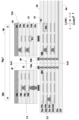
- FIG. 1 is a cross-sectional view of drive module 10 .
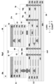
- FIG. 2 is an exploded perspective view of the first laminate 13.
- FIG. 3 is an exploded perspective view of the second laminate 14.
- FIG. 4 is a cross-sectional view of the drive module 10a.
- FIG. 5 is a cross-sectional view of drive module 10b.
- FIG. 6 is a cross-sectional view of drive module 10c.
- FIG. 7 is a cross-sectional view of drive module 10d.
- FIG. 8 is a cross-sectional view of the drive module 10e.
- FIG. 9 is a cross-sectional view of the drive module 10f.
- FIG. 10 is a cross-sectional view of the electronic device 1.
- FIG. 10 is a cross-sectional view of the electronic device 1.
- FIG. 1 is a cross-sectional view of drive module 10 .
- FIG. 2 is an exploded perspective view of the first laminate 13.
- FIG. 3 is an exploded perspective view of the second laminate 14.
- FIG. 1 is a cross-sectional view of drive module 10 .
- FIG. 2 is an exploded perspective view of the first laminate 13.
- FIG. 3 is an exploded perspective view of the second laminate 14.
- the direction in which the first laminated body first main surface S1 and the first laminated body second main surface S2 of the first laminated body 13 are arranged is defined as the vertical direction.
- One of the vertical directions is the first direction DIR1.
- the other vertical direction is the second direction DIR2.
- the first direction DIR1 is upward.
- the second direction DIR2 is downward.
- the left-right direction and the front-rear direction are orthogonal to the up-down direction.
- the left-right direction is perpendicular to the front-rear direction. Note that the vertical direction, the front-rear direction, and the left-right direction in the present embodiment do not have to match the vertical direction, the front-rear direction, and the left-right direction when the drive module 10 is in use.
- X is a part or member of the drive module 10.
- each part of X is defined as follows.
- front of X is meant the front half of X.
- Back of X means the back half of X.
- the left part of X means the left half of X.
- the right part of X means the right half of X.
- Top of X means the top half of X.
- the lower part of X means the lower half of X.
- the leading edge of X means the leading edge of X.
- the trailing end of X means the trailing end of X.
- the left end of X means the end of X in the left direction.
- the right end of X means the end of X in the right direction.
- the upper end of X means the end of X in the upward direction.
- the lower end of X means the lower end of X.
- the front end of X means the front end of X and its vicinity.
- the rear end of X means the rear end of X and its vicinity.
- the left end of X means the left end of X and its vicinity.
- the right end of X means the right end of X and its vicinity.
- the upper end of X means the upper end of X and its vicinity.
- the lower end of X means the lower end of X and its vicinity.
- the drive module 10 is used in wireless communication terminals such as smartphones.
- the drive module 10 comprises a substrate module 11 and magnets 50 .
- the board module 11 includes a first laminate 13, a second laminate 14, a first coil L1, a second coil L2, mounting electrodes 20a to 20f, 26a to 26f, 60a, 60b. , signal conductors 28, 29, 62a, 62b and interlayer connection conductors v6, v15, v31, v32.
- the first laminate 13 has a plate shape. More specifically, as shown in FIG. 1, the first stacked body 13 has a first stacked body first main surface S1 and a first stacked body second main surface S2 arranged vertically. The first laminated body first main surface S1 is located above the first laminated body second main surface S2 (in the first direction DIR1). The first laminated body first main surface S1 and the first laminated body second main surface S2 have a rectangular shape when viewed in the vertical direction.
- the first laminate 13 has a structure in which resin layers 15a to 15e (a plurality of first resin layers) and a protective layer 16 are laminated vertically.
- the protective layer 16 and the resin layers 15a to 15e are arranged in this order from top to bottom.
- the resin layers 15a to 15e have a rectangular shape when viewed in the vertical direction. However, a through hole h is provided in the center of each of the resin layers 15a to 15e so as to penetrate vertically. The through hole h has a rectangular shape when viewed in the vertical direction. A plurality of through holes h form a through hole H by connecting to one. In this manner, as shown in FIG. 1, the first laminate 13 is provided with a through hole H penetrating through the first laminate 13 in the vertical direction.
- the material of the resin layers 15a to 15e is thermoplastic resin.
- Thermoplastic resins are, for example, thermoplastic resins such as liquid crystal polymer and PTFE (polytetrafluoroethylene).
- the material of the resin layers 15a-15e may be polyimide. Therefore, the material of the first laminate 13 is a non-magnetic material.
- the protective layer 16 is a resist layer.
- the protective layer 16 is located on the upper main surface of the resin layer 15a.
- a through hole h is provided in the center of the protective layer 16 so as to penetrate vertically.
- the protective layer 16 protects the first coil conductor 18a located on the upper main surface of the resin layer 15a.
- the protective layer 16 may be formed by attaching an insulating sheet to the upper main surface of the resin layer 15a, or by printing an insulating resin paste on the upper main surface of the resin layer 15a. may be
- the first coil L1 is provided on the first laminate 13, as shown in FIG.
- the first coil L1 has a spiral shape winding around a first coil axis Ax1 extending in the vertical direction.
- the first coil axis Ax1 is positioned in the through hole H when viewed in the vertical direction. Therefore, the first coil L1 winds around the through hole H when viewed in the vertical direction.
- the first coil L1 includes first coil conductors 18a to 18d and interlayer connection conductors v1 to v5, as shown in FIG.
- the first coil conductors 18a-18d are located on the upper main surfaces of the resin layers 15a-15d, respectively. As shown in FIG. 1, each of the first coil conductors 18a to 18d winds around the first coil axis Ax1 when viewed in the vertical direction. As shown in FIG. 2, the first coil conductors 18a and 18c have a spiral shape approaching the center while rotating counterclockwise when viewed downward. When viewed downward, the first coil conductors 18b and 18d have a spiral shape that rotates clockwise and approaches the center.
- the ends of the first coil conductors 18a to 18d on the outer peripheral side are referred to as outer peripheral ends.
- the inner peripheral side end portions of the first coil conductors 18a to 18d are referred to as inner peripheral end portions.
- the mounting electrodes 20a to 20f are located on the lower main surface of the resin layer 15e, as shown in FIG.
- the mounting electrode 20a is positioned near the front left corner of the lower main surface of the resin layer 15e when viewed in the vertical direction.
- the mounting electrode 20b is positioned near the center of the left side of the lower main surface of the resin layer 15e when viewed in the vertical direction.
- the mounting electrode 20c is positioned near the left rear corner of the lower main surface of the resin layer 15e when viewed in the vertical direction.
- the mounting electrode 20d is positioned near the front right corner of the lower main surface of the resin layer 15e when viewed in the vertical direction.
- the mounting electrode 20e is positioned near the center of the right side of the lower main surface of the resin layer 15e when viewed in the vertical direction.
- the mounting electrode 20f is positioned near the right rear corner of the lower main surface of the resin layer 15e when viewed in the vertical direction.
- the mounting electrodes 20a to 20f have a rectangular shape when
- Each of the interlayer connection conductors v1 to v5 vertically penetrates the resin layers 15a to 15e, as shown in FIG.
- the interlayer connection conductor v1 electrically connects the inner peripheral end of the first coil conductor 18a and the inner peripheral end of the first coil conductor 18b.
- the interlayer connection conductor v2 electrically connects the outer peripheral edge of the first coil conductor 18b and the outer peripheral edge of the first coil conductor 18c.
- the interlayer connection conductor v3 electrically connects the inner peripheral end of the first coil conductor 18c and the inner peripheral end of the first coil conductor 18d.
- the interlayer connection conductor v4 and the interlayer connection conductor v5 are connected in series in the vertical direction.
- the interlayer connection conductors v4 and v5 electrically connect the outer peripheral end of the first coil conductor 18d and the mounting electrode 20b.
- the interlayer connection conductor v6 vertically penetrates the resin layers 15a to 15e, as shown in FIG.
- the interlayer connection conductor v6 electrically connects the outer peripheral end of the first coil conductor 18a and the mounting electrode 20a.
- the first coil conductors 18a to 18d and the mounting electrodes 20a to 20f are conductor layers formed by etching metal foils attached to the upper or lower main surfaces of the resin layers 15a to 15e.
- the metal foil is, for example, copper foil.
- the interlayer connection conductors v1 to v6 are via-hole conductors formed by filling conductive paste in through-holes penetrating vertically through the resin layers 15a to 15e and solidifying the conductive paste by heating.
- the interlayer connection conductors v1 to v6 may be through-hole conductors formed by plating the inner peripheral surfaces of through holes penetrating vertically through the resin layers 15a to 15e.
- the second laminated body 14 has a second laminated body first main surface S3 and a second laminated body second main surface S4 arranged vertically.
- the second laminated body first main surface S3 is located above the second laminated body second main surface S4 (in the first direction DIR1).
- the first main surface S3 of the second laminate and the second main surface S4 of the second laminate have a rectangular shape when viewed in the vertical direction.
- the second laminate 14 has a structure in which resin layers 22a to 22f (a plurality of second resin layers) are laminated vertically.
- the resin layers 22a to 22f are arranged in this order from top to bottom.
- the resin layers 22a to 22f have a rectangular shape when viewed in the vertical direction.
- the material of the resin layers 22a-22f is a thermoplastic resin.
- Thermoplastic resins are, for example, thermoplastic resins such as liquid crystal polymer and PTFE (polytetrafluoroethylene).
- the material of the resin layers 22a-22f may be polyimide. Therefore, the material of the second laminate 14 is a non-magnetic material.
- the material of the resin layers 22a-22f (second resin layer) is the same as the material of the resin layers 15a-15e (first resin layer).
- the second coil L2 is provided on the second laminate 14, as shown in FIG.
- the second coil L2 has a helical shape winding around a vertically extending second coil axis Ax2.
- the second coil axis Ax2 is positioned in the through hole H when viewed in the vertical direction.
- the second coil axis Ax2 overlaps the first coil axis Ax1 when viewed in the vertical direction.
- the second coil L2 overlaps the first coil L1 when viewed in the vertical direction.
- the second coil L2 includes second coil conductors 24a to 24d and interlayer connection conductors v11 to v14, as shown in FIG.
- the second coil conductors 24a-24d are located on the upper main surfaces of the resin layers 22b-22e, respectively.
- Each of the second coil conductors 24a to 24d winds around the second coil axis Ax2 when viewed in the vertical direction.
- the second coil conductors 24a and 24c have a spiral shape approaching the center while rotating counterclockwise when viewed downward. When viewed downward, the second coil conductors 24b and 24d have a spiral shape that rotates clockwise and approaches the center.
- the ends of the second coil conductors 24a to 24d on the outer peripheral side are referred to as outer peripheral ends.
- the ends on the inner peripheral side of the second coil conductors 24a to 24d are called inner peripheral ends.
- the mounting electrodes 26a to 26f are located on the upper main surface of the resin layer 22a.
- the mounting electrode 26a is positioned near the front left corner of the upper main surface of the resin layer 22a when viewed in the vertical direction.
- the mounting electrode 26b is positioned near the center of the left side of the upper main surface of the resin layer 22a when viewed in the vertical direction.
- the mounting electrode 26c is positioned near the left rear corner of the upper main surface of the resin layer 22a when viewed in the vertical direction.
- Each of the mounting electrodes 26d to 26f is positioned to the right of the mounting electrodes 26a to 26c when viewed in the vertical direction.
- the mounting electrodes 26a to 26f have a rectangular shape when viewed in the vertical direction.
- Each of the interlayer connection conductors v11 to v14 vertically penetrates the resin layers 22a to 22d.
- the interlayer connection conductor v11 electrically connects the mounting electrode 26b and the outer peripheral end of the second coil conductor 24a.
- the interlayer connection conductor v12 electrically connects the inner peripheral end of the second coil conductor 24a and the inner peripheral end of the second coil conductor 24b.
- the interlayer connection conductor v13 electrically connects the outer peripheral end of the second coil conductor 24b and the outer peripheral end of the second coil conductor 24c.
- the interlayer connection conductor v14 electrically connects the inner peripheral end of the second coil conductor 24c and the inner peripheral end of the second coil conductor 24d.
- the signal conductor 28 is located on the upper main surface of the resin layer 22d.
- the signal conductor 28 has a linear shape extending in the left-right direction.
- the left end of the signal conductor 28 overlaps the mounting electrode 26a when viewed in the vertical direction.
- the signal conductor 29 is located on the upper main surface of the resin layer 22e.
- the signal conductor 29 has a linear shape extending in the left-right direction.
- the left end of the signal conductor 29 is connected to the outer peripheral end of the second coil conductor 24d.
- the interlayer connection conductor v15 vertically penetrates the resin layers 22a to 22c.
- the interlayer connection conductor v15 electrically connects the left end of the signal conductor 28 and the mounting electrode 26a.
- the mounting electrodes 60a and 60b are located on the first main surface S3 of the second laminate, as shown in FIG. Accordingly, the mounting electrodes 60a and 60b are located on the upper main surface of the resin layer 22a. As shown in FIG. 1, the mounting electrodes 60a and 60b overlap the through holes H when viewed in the vertical direction. The mounting electrodes 60a and 60b are arranged in this order from left to right. The mounting electrodes 60a and 60b have a rectangular shape when viewed in the vertical direction.
- the signal conductor 62a is located on the upper main surface of the resin layer 22f, as shown in FIG.
- the signal conductor 62a has a linear shape extending in the left-right direction.
- the left end of the signal conductor 62a overlaps the mounting electrode 60a when viewed in the vertical direction.
- the signal conductor 62b is located on the upper main surface of the resin layer 22f.
- the signal conductor 62b has a linear shape extending in the left-right direction.
- the left end of the signal conductor 62b overlaps the mounting electrode 60b when viewed in the vertical direction.
- the interlayer connection conductor v31 vertically penetrates the resin layers 22a to 22e.
- the interlayer connection conductor v31 electrically connects the mounting electrode 60a and the left end of the signal conductor 62a.
- the interlayer connection conductor v32 vertically penetrates the resin layers 22a to 22e.
- the interlayer connection conductor v32 electrically connects the mounting electrode 60b and the left end of the signal conductor 62b.
- the second coil conductors 24a-24d, the signal conductors 28, 29, 62a, 62b and the mounting electrodes 60a, 60b are formed by etching a metal foil attached to the upper main surface of the resin layers 22a-22e. It is a conductive layer.
- the metal foil is, for example, copper foil.
- the interlayer connection conductors v11 to v15, v31, and v32 are via-hole conductors formed by filling conductive paste in through-holes vertically penetrating the resin layers 22a to 22e and solidifying the conductive paste by heating.
- the interlayer connection conductors v11 to v15, v31, and v32 may be through-hole conductors formed by plating the inner peripheral surfaces of through holes penetrating the resin layers 22a to 22e in the vertical direction. .
- the first laminate 13 is mounted on the second laminate first main surface S3 of the second laminate 14 .
- the second stacked body 14 is located below the first stacked body 13 (in the second direction DIR2).
- the second laminate 14 overlaps the first laminate 13 when viewed in the vertical direction.
- the first stacked body 13 is positioned within a region surrounded by the outer edges of the second stacked body 14 when viewed in the vertical direction. That is, the area of the second stacked body 14 seen in the vertical direction is larger than the area of the first stacked body 13 seen in the vertical direction.
- the first laminate 13 does not protrude from the outer edge of the second laminate 14 .
- Each of the mounting electrodes 20a to 20f is fixed to the mounting electrodes 26a to 26f with a conductive bonding material.
- the first coil L1 is electrically connected to the second coil L2 by mounting the first laminate 13 on the second laminate 14 with the conductive bonding material. More precisely, the first coil L1 is connected in series with the second coil L2.
- the conductive bonding material is, for example, solder.
- the magnet 50 is located above the first coil L1 (in the first direction DIR1), as shown in FIG.
- the magnet 50 overlaps the first coil L1 when viewed in the vertical direction.
- Magnet 50 extends in the left-right direction.
- the left side of magnet 50 is the north pole.
- the right portion of magnet 50 is the south pole.
- Magnet 50 is a permanent magnet.
- the magnet 50 may be an electromagnet.
- the magnetic sensor 30 detects the magnetic force of the magnet 50.
- the magnetic sensor 30 is a mounted component mounted on the first main surface S3 of the second laminate.
- the magnetic sensor 30 includes a magnetic sensor body 32 and magnetic sensor mounting electrodes 34a and 34b.
- the magnetic sensor main body 32 incorporates a magnetic sensor.
- the magnetic sensor main body 32 has a rectangular parallelepiped shape.
- the magnetic sensor mounting electrodes 34 a and 34 b are located on the lower surface of the magnetic sensor main body 32 .
- Each of the magnetic sensor mounting electrodes 34a, 34b is fixed to the mounting electrodes 60a, 60b with a conductive bonding material such as solder.
- the magnetic sensor 30 is surrounded by the first coil L1 and the second coil L2 when viewed in the vertical direction. Accordingly, at least a portion of the magnetic sensor 30 is positioned within the through hole H. As shown in FIG.
- the upper end of the magnetic sensor 30 (the end in the first direction DIR1) is positioned below the first main surface S1 of the first laminate (second direction DIR2). That is, the upper surface of the magnetic sensor main body 32 of the magnetic sensor 30 is positioned below the first main surface S1 of the first laminate. Therefore, the magnetic sensor 30 does not protrude upward from the first main surface of the first laminate.
- the average number of turns of the first coil conductors 18a to 18d is defined as the number of turns N1 of the first coil conductors 18a to 18d.
- the average number of turns of the second coil conductors 24a-24d is defined as the number of turns N2 of the second coil conductors 24a-24d.
- Each of the number of turns of the first coil conductors 18a-18d is approximately 1.5 turns. Therefore, the number of turns N1 of the first coil conductors 18a to 18d is approximately 1.5 turns.
- Each of the number of turns of the second coil conductors 24a-24d is approximately 1.5 turns. Therefore, the number of turns N2 of the second coil conductors 24a to 24d is approximately 1.5 turns. Therefore, the number of turns N1 of the first coil conductors 18a-18d is substantially equal to the number of turns N2 of the second coil conductors 24a-24d.
- the direction orthogonal to the direction in which the first coil conductors 18a to 18d and the second coil conductors 24a to 24d extend when viewed in the vertical direction is the line width direction.
- the average width of the first coil conductors 18a to 18d in the line width direction is defined as the width W1 of the first coil conductors 18a to 18d in the line width direction.
- the average width of the second coil conductors 24a to 24d in the line width direction is defined as the width W2 of the second coil conductors 24a to 24d in the line width direction.
- the width W1 is smaller than the width W2.
- the product X1 of the number of turns N1 of the first coil conductors 18a to 18d and the width W1 in the line width direction of the first coil conductors 18a to 18d is the number of turns N2 of the second coil conductors 24a to 24d and the number of turns N2 of the second coil conductors 24a to 24d. It is smaller than the product X2 with the width W2 of 24d in the line width direction.
- the drive module 10 as described above includes a control circuit (not shown).
- the magnetic sensor 30, the first coil L1 and the second coil L2 are electrically connected to a control circuit.
- the magnetic sensor 30 generates an output signal according to the magnitude of the magnetic force of the magnet 50 detected by the magnetic sensor 30 .
- the control circuit controls the magnitude of the current that flows through the first coil L1 and the second coil L2. For example, when viewed downward, when a clockwise current flows through the first coil L1 and the second coil L2, a forward current flows through the conductors positioned to the left of the first coil L1 and the second coil L2. A current flows in the rearward direction through the conductors located on the right side of the first coil L1 and the second coil L2.
- the lines of magnetic force are emitted from the N pole and the lines of magnetic force are applied to the S pole. Therefore, when a current flows forward in the conductors located on the left side of the first coil L1 and the second coil L2, the conductors located on the left side of the first coil L1 and the second coil L2 are subjected to the Lorentz force in the left direction. receive. When a current flows backward through the conductors located on the right side of the first coil L1 and the second coil L2, the conductors located on the right side of the first coil L1 and the second coil L2 receive Lorentz force in the left direction. . That is, the first coil L1 and the second coil L2 receive force from the magnet 50 in the left direction.
- the magnet 50 receives force rightward from the first coil L1 and the second coil L2. As a result, the magnet 50 is displaced to the right with respect to the first coil L1 and the second coil L2. However, the first coil L1 and the second coil L2 may be displaced leftward with respect to the magnet 50 .
- the conductors positioned on the right side of the first coil L1 and the second coil L2 receive Lorentz force in the right direction.
- the first coil L1 and the second coil L2 receive force from the magnet 50 in the right direction.
- the magnet 50 receives force in the left direction from the first coil L1 and the second coil L2.
- the magnet 50 is displaced leftward with respect to the first coil L1 and the second coil L2.
- the first coil L ⁇ b>1 and the second coil L ⁇ b>2 may be displaced to the right with respect to the magnet 50 .
- the magnetic force generated by the first coil L1 and the second coil L2 changes the position of the magnet 50 with respect to the first coil L1 and the second coil L2.
- the board module 11 it is possible to reduce the DC resistance value of the second coil L2 and improve the inductance value of the second coil L2. More specifically, the area of the second stacked body 14 seen in the vertical direction is larger than the area of the first stacked body 13 seen in the vertical direction. Therefore, it is easy to make the size of the second coil conductors 24a to 24d larger than the size of the first coil conductors 18a to 18d. Therefore, the product X1 of the number of turns N1 of the first coil conductors 18a to 18d and the width W1 in the line width direction of the first coil conductors 18a to 18d is the number of turns N2 of the second coil conductors 24a to 24d and the second coil conductors.
- the magnetic force generated by the first coil L1 and the second coil L2 changes the position of the magnet 50 with respect to the first coil L1 and the second coil L2.
- a large current flows through the first coil L1 and the second coil L2. Therefore, in the drive module 10, it is desired to reduce the DC resistance value of the second coil L2. Therefore, the product X1 of the number of turns N1 of the first coil conductors 18a to 18d and the width W1 in the line width direction of the first coil conductors 18a to 18d is the number of turns N2 of the second coil conductors 24a to 24d and the second coil conductors. It is smaller than the product X2 with the width W2 of 24a to 24d in the line width direction. Thereby, the DC resistance value of the second coil L2 is reduced.
- the substrate module 11 has a structure suitable for the drive module 10. As shown in FIG.
- the upper end of the magnetic sensor 30 (the end in the first direction DIR1) is located below the first main surface S1 of the first laminate (second direction DIR2). That is, the upper surface of the magnetic sensor main body 32 of the magnetic sensor 30 is positioned below the first main surface S1 of the first laminate. Therefore, the magnetic sensor 30 does not protrude upward from the first main surface S1 of the first laminate. As a result, the size of the substrate module 11 can be reduced in the vertical direction.
- FIG. 4 is a cross-sectional view of the drive module 10a.
- the drive module 10a differs from the drive module 10 in the number of turns N2 of the second coil conductors 24a to 24d. More specifically, the number of turns N1 of the first coil conductors 18a-18d is less than the number of turns N2 of the second coil conductors 24a-24d. In other words, the number of turns N2 of the second coil conductors 24a-24d is greater than the number of turns N1 of the first coil conductors 18a-18d.
- the width W1 of the first coil conductors 18a to 18d in the line width direction is smaller than the width W2 of the second coil conductors 24a to 24d in the line width direction.
- the product X1 of the number of turns N1 of the first coil conductors 18a to 18d and the width W1 in the line width direction of the first coil conductors 18a to 18d is the number of turns N2 of the second coil conductors 24a to 24d and the second coil It is smaller than the product X2 with the width W2 of the conductors 24a to 24d in the line width direction.
- the rest of the structure of the drive module 10a is the same as that of the drive module 10, so the explanation is omitted.
- the driving module 10 a can have the same effects as the driving module 10 .
- the number of turns N1 of the first coil conductors 18a-18d is less than the number of turns N2 of the second coil conductors 24a-24d. In other words, the number of turns N2 of the second coil conductors 24a-24d is greater than the number of turns N1 of the first coil conductors 18a-18d. Thereby, the inductance value of the second coil L2 can be further improved.
- FIG. 5 is a cross-sectional view of drive module 10b.
- the drive module 10b differs from the drive module 10a in the width W2 in the line width direction of the second coil conductors 24a to 24d. More specifically, the width W1 of the first coil conductors 18a to 18d in the line width direction is equal to the width W2 of the second coil conductors 24a to 24d in the line width direction. However, in the drive module 10b, similarly to the drive module 10a, the number of turns N1 of the first coil conductors 18a-18d is smaller than the number of turns N2 of the second coil conductors 24a-24d.
- the product X1 of the number of turns N1 of the first coil conductors 18a to 18d and the width W1 in the line width direction of the first coil conductors 18a to 18d is the number of turns N2 of the second coil conductors 24a to 24d and the second coil It is smaller than the product X2 with the width W2 of the conductors 24a to 24d in the line width direction.
- the rest of the structure of the drive module 10b is the same as that of the drive module 10a, so the description is omitted.
- the drive module 10b can have the same effects as the drive module 10a.
- FIG. 6 is a cross-sectional view of drive module 10c.
- the drive module 10c differs from the drive module 10 in that the first laminate 13 and the second laminate 14 are integrated by thermocompression bonding. More specifically, the resin layer 15e of the first laminate 13 and the resin layer 22a of the second laminate 14 are integrated by thermocompression bonding. Other structures of the drive module 10c are the same as those of the drive module 10, so description thereof is omitted. The drive module 10c can have the same effects as the drive module 10. FIG.
- FIG. 7 is a cross-sectional view of drive module 10d.
- the drive module 10d differs from the drive module 10b in the shape of the first coil L1. More specifically, the first coil L1 overlaps the innermost portion and the second innermost portion of the second coil L2 when viewed in the vertical direction. Therefore, the outermost portion of the second coil L2 does not overlap the first coil L1 when viewed in the vertical direction.
- Other structures of the drive module 10d are the same as those of the drive module 10, so description thereof is omitted.
- the drive module 10 d can have the same effects as the drive module 10 .
- FIG. 8 is a cross-sectional view of the drive module 10e.
- the drive module 10e differs from the drive module 10 in that it further includes a mounting component 70, mounting electrodes 80a and 80b, and interlayer connection conductors v41 and v42.
- the mounting electrodes 80a and 80b are located on the first main surface S3 of the second laminate.
- the interlayer connection conductor v41 vertically penetrates the resin layers 22a to 22d.
- the interlayer connection conductor v41 electrically connects the mounting electrode 80a and the right end of the signal conductor .
- the interlayer connection conductor v42 vertically penetrates the resin layers 22a to 22e.
- the interlayer connection conductor v42 electrically connects the mounting electrode 80b and the right end of the signal conductor 62b.
- the mounted component 70 is an electronic component mounted on the second laminate 14 .
- the mounting component 70 is, for example, a control circuit that controls the magnitude of the current that flows through the first coil L1 and the second coil L2 based on the output signal generated by the magnetic sensor 30 .
- the mounted component 70 is, for example, an IC (Integrated Circuit).
- the mounting component 70 includes a mounting component body 72 and mounting component electrodes 74a and 74b.
- the mounting component main body 72 has a rectangular parallelepiped shape. Mounted component electrodes 74 a and 74 b are provided on the lower surface of mounted component body 72 .
- the mounting component electrodes 74a and 74b are fixed to the mounting electrodes 80a and 80b with a conductive bonding material, respectively. In this way, by mounting the mounted component 70 on the second laminate 14 with the conductive bonding material, the mounted component 70 and the second coil L2 are electrically connected to each other, and the mounted component 70 and the magnetic coupling are electrically connected to each other.
- the sensor 30 is electrically connected to each other.
- the conductive bonding material is, for example, solder.
- Other structures of the drive module 10e are the same as those of the drive module 10, so description thereof is omitted.
- the driving module 10 e can have the same effects as the driving module 10 .
- interlayer connection conductor v31 and the signal conductor 62a may be electrically connected to the mounting component 70 via an interlayer connection conductor (not shown).
- signal conductor 29 may be electrically connected to the mounting component 70 via an interlayer connection conductor (not shown).
- FIG. 9 is a cross-sectional view of the drive module 10f.
- the drive module 10f includes two sets of drive modules 10g and 10h.
- Drive modules 10 g and 10 h have the same structure as drive module 10 .
- the structure of the drive module 10h is symmetrical with the structure of the drive module 10g.
- the second laminate 14 of the drive module 10g and the second laminate 14 of the drive module 10h are connected to form one laminate.
- the drive modules 10g and 10h are integrated. Therefore, when the drive module 10f is attached to the electronic device, the drive module 10g and the drive module 10h are positioned more accurately than when the two drive modules are separately attached to the electronic device. Become.
- FIG. 10 is a cross-sectional view of the electronic device 1.
- the electronic device 1 is a wireless communication terminal such as a smartphone.
- the electronic device 1 includes a drive module 10 , a battery 100 , a circuit board 110 and a housing 120 .
- the drive module 10 is electrically connected to the circuit board 110 via a connector.
- the substrate module 11 of the drive module 10 is flexible and therefore bent.
- the deformation of the board module 11 may be plastic deformation, elastic deformation, or both plastic deformation and elastic deformation.
- the battery 100 is located on the upper main surface of the circuit board 110 .
- the battery 100 is electrically connected to the circuit board 110 by wiring (not shown).
- Battery 100 supplies power to drive module 10 through circuit board 110 .
- the housing 120 houses the drive module 10 , the battery 100 and the circuit board 110 .
- the drive modules according to the present invention are not limited to the drive modules 10, 10a to 10f, and can be modified within the scope of the subject matter.
- the configuration of the drive modules 10, 10a to 10f may be combined arbitrarily.
- the board modules according to the present invention are not limited to the board modules 11, 11a to 11f, and can be modified within the scope of the gist thereof.
- the configurations of the board modules 11, 11a to 11f may be combined arbitrarily.
- the material of the resin layers 15a to 15e and 22a to 22f may be a material other than thermoplastic resin.
- the magnetic sensor 30 does not have to be surrounded by the first coil L1 and the second coil L2 when viewed in the vertical direction.
- the magnetic sensor 30 does not have to be positioned within the through hole H.
- the magnetic sensor 30 may be positioned to the right of the first stack 13, for example.
- the upper surface of the magnetic sensor 30 may be positioned above the first main surface S1 of the first laminate.
- the material of the resin layers 22a-22f may be different from the material of the resin layers 15a-15e (first resin layer).
- the substrate module 11 may be used in devices other than the drive modules 10, 10a to 10f.
- the first coil L1 and the second coil L2 of the board module 11 may function as antennas, for example.
- the first coil L1 and the second coil L2 may transmit and receive electric power, or transmit and receive high-frequency signals.
- the signal conductors 62a and 62b may be positioned on the lower main surface of the resin layer 22f.
- a protective layer is provided under the resin layer 22f to protect the signal conductors 62a and 62b.
- the width of the signal conductors 28 and 29 in the line width direction may be larger than the width W1 of the first coil conductors 18a to 18d in the line width direction. That is, the width of the signal conductors 28 and 29 in the line width direction may be equal to the width W2 of the second coil conductors 24a to 24d in the line width direction. Thereby, the resistance of the signal conductors 28 and 29 is reduced.
- the downward direction may be the first direction DIR1 and the upward direction may be the second direction DIR2.
- first coil L1 may include one or more first coil conductors.
- the second coil L2 may include one or more second coil conductors.
- the electronic device 1 may include any one of the drive modules 10a to 10f instead of the drive module 10.
Landscapes
- Engineering & Computer Science (AREA)
- Power Engineering (AREA)
- Microelectronics & Electronic Packaging (AREA)
- Coils Or Transformers For Communication (AREA)
- Parts Printed On Printed Circuit Boards (AREA)
- Coils Of Transformers For General Uses (AREA)
Priority Applications (2)
| Application Number | Priority Date | Filing Date | Title |
|---|---|---|---|
| CN202290000246.7U CN220357894U (zh) | 2021-08-19 | 2022-07-20 | 基板模块、驱动模块及电子设备 |
| JP2023540833A JP7351440B2 (ja) | 2021-08-19 | 2022-07-20 | 基板モジュール、駆動モジュール及び電子機器 |
Applications Claiming Priority (2)
| Application Number | Priority Date | Filing Date | Title |
|---|---|---|---|
| JP2021-133733 | 2021-08-19 | ||
| JP2021133733 | 2021-08-19 |
Publications (1)
| Publication Number | Publication Date |
|---|---|
| WO2023021908A1 true WO2023021908A1 (ja) | 2023-02-23 |
Family
ID=85240484
Family Applications (1)
| Application Number | Title | Priority Date | Filing Date |
|---|---|---|---|
| PCT/JP2022/028170 Ceased WO2023021908A1 (ja) | 2021-08-19 | 2022-07-20 | 基板モジュール、駆動モジュール及び電子機器 |
Country Status (3)
| Country | Link |
|---|---|
| JP (1) | JP7351440B2 (https=) |
| CN (1) | CN220357894U (https=) |
| WO (1) | WO2023021908A1 (https=) |
Citations (4)
| Publication number | Priority date | Publication date | Assignee | Title |
|---|---|---|---|---|
| JPH07272935A (ja) * | 1995-03-20 | 1995-10-20 | Taiyo Yuden Co Ltd | 積層チップインダクタおよびその製造方法 |
| JP2002208515A (ja) * | 2001-01-09 | 2002-07-26 | Murata Mfg Co Ltd | 積層型インダクタ |
| JP2014170869A (ja) * | 2013-03-05 | 2014-09-18 | Omron Automotive Electronics Co Ltd | 磁気デバイス |
| WO2019021764A1 (ja) * | 2017-07-24 | 2019-01-31 | 株式会社村田製作所 | アクチュエータ、およびアクチュエータの製造方法 |
-
2022
- 2022-07-20 CN CN202290000246.7U patent/CN220357894U/zh active Active
- 2022-07-20 JP JP2023540833A patent/JP7351440B2/ja active Active
- 2022-07-20 WO PCT/JP2022/028170 patent/WO2023021908A1/ja not_active Ceased
Patent Citations (4)
| Publication number | Priority date | Publication date | Assignee | Title |
|---|---|---|---|---|
| JPH07272935A (ja) * | 1995-03-20 | 1995-10-20 | Taiyo Yuden Co Ltd | 積層チップインダクタおよびその製造方法 |
| JP2002208515A (ja) * | 2001-01-09 | 2002-07-26 | Murata Mfg Co Ltd | 積層型インダクタ |
| JP2014170869A (ja) * | 2013-03-05 | 2014-09-18 | Omron Automotive Electronics Co Ltd | 磁気デバイス |
| WO2019021764A1 (ja) * | 2017-07-24 | 2019-01-31 | 株式会社村田製作所 | アクチュエータ、およびアクチュエータの製造方法 |
Also Published As
| Publication number | Publication date |
|---|---|
| CN220357894U (zh) | 2024-01-16 |
| JPWO2023021908A1 (https=) | 2023-02-23 |
| JP7351440B2 (ja) | 2023-09-27 |
Similar Documents
| Publication | Publication Date | Title |
|---|---|---|
| JP5970719B2 (ja) | 回路基板 | |
| JP6156610B2 (ja) | 電子機器、およびアンテナ素子 | |
| CN208016128U (zh) | 多层基板及电子设备 | |
| JP6256820B2 (ja) | フレキシブルプリント配線板及び該フレキシブルプリント配線板の製造方法 | |
| US11424062B2 (en) | Flexible inductor | |
| US9401533B2 (en) | Flat cable | |
| US10225928B2 (en) | Flexible board and electronic device | |
| KR20160013015A (ko) | 센서 기판 | |
| WO2014115433A1 (ja) | コイル部品および電子機器 | |
| WO2014199886A1 (ja) | 通信装置および電子機器 | |
| WO2023021908A1 (ja) | 基板モジュール、駆動モジュール及び電子機器 | |
| JP6460290B2 (ja) | Dc/dcコンバータモジュール | |
| JPWO2018173666A1 (ja) | 多層基板 | |
| US12464653B2 (en) | Circuit board and electronic-component-equipped circuit board | |
| CN220252959U (zh) | 线圈部件 | |
| CN218241537U (zh) | 线圈部件以及驱动模块 | |
| JP7306604B2 (ja) | 駆動モジュール及び電子機器 | |
| US20150116060A1 (en) | High-frequency signal transmission line and electronic device | |
| JP5569011B2 (ja) | アンテナ部品 | |
| JP2022162293A (ja) | 回路基板及び電子機器 | |
| US20250142739A1 (en) | Electronic Control Unit Capable of Suppressing an Increase in Size of a Board | |
| JP2023156834A (ja) | 多層基板及び電子機器 | |
| CN105704910B (zh) | 软硬结合板及终端 | |
| JP2008227425A (ja) | 電気回路基板 |
Legal Events
| Date | Code | Title | Description |
|---|---|---|---|
| 121 | Ep: the epo has been informed by wipo that ep was designated in this application |
Ref document number: 22858230 Country of ref document: EP Kind code of ref document: A1 |
|
| WWE | Wipo information: entry into national phase |
Ref document number: 2023540833 Country of ref document: JP |
|
| WWE | Wipo information: entry into national phase |
Ref document number: 202290000246.7 Country of ref document: CN |
|
| NENP | Non-entry into the national phase |
Ref country code: DE |
|
| 122 | Ep: pct application non-entry in european phase |
Ref document number: 22858230 Country of ref document: EP Kind code of ref document: A1 |