WO2023021643A1 - 応力緩和構造 - Google Patents
応力緩和構造 Download PDFInfo
- Publication number
- WO2023021643A1 WO2023021643A1 PCT/JP2021/030314 JP2021030314W WO2023021643A1 WO 2023021643 A1 WO2023021643 A1 WO 2023021643A1 JP 2021030314 W JP2021030314 W JP 2021030314W WO 2023021643 A1 WO2023021643 A1 WO 2023021643A1
- Authority
- WO
- WIPO (PCT)
- Prior art keywords
- electronic substrate
- porous layer
- metal pattern
- electronic
- stress relaxation
- Prior art date
- Legal status (The legal status is an assumption and is not a legal conclusion. Google has not performed a legal analysis and makes no representation as to the accuracy of the status listed.)
- Ceased
Links
Images




Classifications
-
- H—ELECTRICITY
- H10—SEMICONDUCTOR DEVICES; ELECTRIC SOLID-STATE DEVICES NOT OTHERWISE PROVIDED FOR
- H10W—GENERIC PACKAGES, INTERCONNECTIONS, CONNECTORS OR OTHER CONSTRUCTIONAL DETAILS OF DEVICES COVERED BY CLASS H10
- H10W70/00—Package substrates; Interposers; Redistribution layers [RDL]
- H10W70/60—Insulating or insulated package substrates; Interposers; Redistribution layers
-
- H—ELECTRICITY
- H10—SEMICONDUCTOR DEVICES; ELECTRIC SOLID-STATE DEVICES NOT OTHERWISE PROVIDED FOR
- H10W—GENERIC PACKAGES, INTERCONNECTIONS, CONNECTORS OR OTHER CONSTRUCTIONAL DETAILS OF DEVICES COVERED BY CLASS H10
- H10W74/00—Encapsulations, e.g. protective coatings
- H10W74/40—Encapsulations, e.g. protective coatings characterised by their materials
- H10W74/47—Encapsulations, e.g. protective coatings characterised by their materials comprising organic materials, e.g. plastics or resins
-
- H—ELECTRICITY
- H05—ELECTRIC TECHNIQUES NOT OTHERWISE PROVIDED FOR
- H05K—PRINTED CIRCUITS; CASINGS OR CONSTRUCTIONAL DETAILS OF ELECTRIC APPARATUS; MANUFACTURE OF ASSEMBLAGES OF ELECTRICAL COMPONENTS
- H05K3/00—Apparatus or processes for manufacturing printed circuits
- H05K3/22—Secondary treatment of printed circuits
- H05K3/28—Applying non-metallic protective coatings
-
- H—ELECTRICITY
- H10—SEMICONDUCTOR DEVICES; ELECTRIC SOLID-STATE DEVICES NOT OTHERWISE PROVIDED FOR
- H10W—GENERIC PACKAGES, INTERCONNECTIONS, CONNECTORS OR OTHER CONSTRUCTIONAL DETAILS OF DEVICES COVERED BY CLASS H10
- H10W42/00—Arrangements for protection of devices
- H10W42/121—Arrangements for protection of devices protecting against mechanical damage
-
- H—ELECTRICITY
- H10—SEMICONDUCTOR DEVICES; ELECTRIC SOLID-STATE DEVICES NOT OTHERWISE PROVIDED FOR
- H10W—GENERIC PACKAGES, INTERCONNECTIONS, CONNECTORS OR OTHER CONSTRUCTIONAL DETAILS OF DEVICES COVERED BY CLASS H10
- H10W74/00—Encapsulations, e.g. protective coatings
- H10W74/10—Encapsulations, e.g. protective coatings characterised by their shape or disposition
-
- H—ELECTRICITY
- H10—SEMICONDUCTOR DEVICES; ELECTRIC SOLID-STATE DEVICES NOT OTHERWISE PROVIDED FOR
- H10W—GENERIC PACKAGES, INTERCONNECTIONS, CONNECTORS OR OTHER CONSTRUCTIONAL DETAILS OF DEVICES COVERED BY CLASS H10
- H10W74/00—Encapsulations, e.g. protective coatings
- H10W74/40—Encapsulations, e.g. protective coatings characterised by their materials
-
- H—ELECTRICITY
- H10—SEMICONDUCTOR DEVICES; ELECTRIC SOLID-STATE DEVICES NOT OTHERWISE PROVIDED FOR
- H10W—GENERIC PACKAGES, INTERCONNECTIONS, CONNECTORS OR OTHER CONSTRUCTIONAL DETAILS OF DEVICES COVERED BY CLASS H10
- H10W76/00—Containers; Fillings or auxiliary members therefor; Seals
- H10W76/10—Containers or parts thereof
-
- H—ELECTRICITY
- H10—SEMICONDUCTOR DEVICES; ELECTRIC SOLID-STATE DEVICES NOT OTHERWISE PROVIDED FOR
- H10W—GENERIC PACKAGES, INTERCONNECTIONS, CONNECTORS OR OTHER CONSTRUCTIONAL DETAILS OF DEVICES COVERED BY CLASS H10
- H10W76/00—Containers; Fillings or auxiliary members therefor; Seals
- H10W76/60—Seals
Definitions
- the present disclosure relates to technology for increasing the thermal stress resistance of electronic boards on which electronic components are mounted.
- the stress is concentrated at the edges or corners of the structure.
- the adhesives or resins may be removed from the ends of the structure due to differences in thermal expansion coefficients due to temperature cycles or volumetric changes due to moisture absorption and desorption.
- problems such as peeling of the adhesive or cracks in the adhesive or resin.
- a box-shaped member may be used as a cap and fixed by adhesion. Even in this case, there is a problem that the cap may be peeled off due to thermal stress, or the cap may be removed due to the expansion of the internal moisture due to the hollow structure and the formation of water vapor when heated.
- Patent Document 1 describes that the corners of the coating material are rounded in order to improve the adhesion of the sealing resin to the coating material on the substrate. This suppresses peeling of the sealing resin due to temperature cycles or thermal stress that occurs during customer mounting.
- Patent Document 1 is expected to improve adhesion when there is a sealing resin by devising the shape of the coating material, but it cannot be applied when there is no sealing resin. Moreover, there is a problem that the effect is small when a high thermal stress is applied.
- the present disclosure has been made to solve the above problems, and aims to increase the thermal stress resistance of electronic boards on which electronic components are mounted.
- One stress relaxation structure of the present disclosure includes an electronic substrate, a metal pattern formed on the top surface of the electronic substrate, an electronic component formed on the top surface of the metal pattern, corners of the metal pattern, and corners of the metal pattern.
- a porous layer provided on at least one of the corners of the resist when covered with the resist, the surface layer of the outer periphery of the electronic substrate, and the upper surface of the outer periphery of the electronic substrate, the upper surface of the electronic substrate, the metal pattern, and the electronic component. and a sealing resin for sealing.
- the porous layer increases the adhesion between the sealing resin and the electronic substrate or the like, so that the thermal stress resistance of the electronic substrate on which the electronic component is mounted can be increased.
- FIG. 2 is a cross-sectional view showing the stress relaxation structure of Embodiment 1;
- FIG. FIG. 8 is a cross-sectional view showing a stress relaxation structure according to a second embodiment;
- FIG. 11 is a cross-sectional view showing a stress relaxation structure according to a third embodiment;
- FIG. 11 is a cross-sectional view showing a stress relaxation structure according to a third embodiment;
- FIG. 11 is a cross-sectional view showing a stress relaxation structure according to a fourth embodiment;
- FIG. 11 is a cross-sectional view showing a stress relaxation structure according to a fourth embodiment;
- FIG. 11 is a cross-sectional view showing a stress relaxation structure according to a fifth embodiment;
- FIG. 11 is a cross-sectional view showing a stress relaxation structure according to a fifth embodiment
- FIG. 12 is a cross-sectional view showing a stress relaxation structure according to a sixth embodiment
- FIG. 21 is a cross-sectional view showing a stress relaxation structure according to Embodiment 7
- FIG. 21 is a cross-sectional view showing a stress relaxation structure according to an eighth embodiment
- FIG. 1 is a cross-sectional view showing a stress relaxation structure 1001 of Embodiment 1.
- FIG. Stress relaxation structure 1001 includes electronic substrate 101 , metal pattern 102 , resist 103 , porous layer 104 , electronic component 105 and sealing resin 106 .
- a circuit is constructed by drawing a pattern with metal on the electronic substrate 101 . Also, metal pads for mounting electronic components 105 are provided on the electronic substrate 101 . These patterns and metal pads are collectively referred to herein as metal pattern 102 .
- Resist 103 is for protecting metal pattern 102 from solder or other foreign matter during the process of mounting electronic component 105 .
- Electronic components 105 are, for example, semiconductor elements, resistors or capacitors.
- the corners of the resist 103 where stress concentrates are covered with the porous layer 104, thereby relieving the stress and enhancing the adhesion of the sealing resin 106.
- the porous layer 104 is made of organic resin having a porous structure.
- the porous structure of the porous layer 104 is a monolithic structure, a mesoporous structure, a honeycomb structure, or a layered structure.
- the porous structure provides a stress relieving effect.
- the sealing resin 106 since the sealing resin 106 enters the pores of the porous layer 104, the adhesion area of the sealing resin 106 increases, and the sealing resin 106 comes into contact with the porous layer 104 three-dimensionally. The effect is obtained, and the adhesion between the porous layer 104 and the sealing resin 106 is enhanced.
- the adhesion between the porous layer 104 and the sealing resin 106 is enhanced.
- the organic resin material used for the porous layer 104 has a Young's modulus lower than that of the sealing resin 106, so that a greater stress relaxation effect can be obtained.
- epoxy compound epoxy resin
- acrylic compound acrylic resin
- Epoxy resins used for the porous layer 104 include bisphenol A-type epoxy resins, bisphenol F-type epoxy resins, cresol novolac-type epoxy resins, diphenylmethane-type epoxy resins, and epoxy resins containing a plurality of aromatic rings.
- One of the epoxy resins listed here may be used alone, or two or more thereof may be used in combination.
- the curing agent used for the porous layer 104 includes aromatic amines, aromatic acid anhydrides, aliphatic amines, or modified products thereof.
- One of the curing agents listed here may be used alone, or two or more thereof may be used in combination.
- the method for forming the porous layer 104 is as follows. First, a mixture containing an organic resin material, a curing agent, and a pore-forming material is formed on an arbitrary location on the electronic substrate 101 using a coating method such as a printing method or a dipping method. The mixture is then heat cured to form a porous layer with a plurality of pores. The pore-forming material is then removed by washing with water or an organic solvent. Thus, the porous layer 104 is formed.
- thermal curing is mentioned above, other known curing methods may be used, such as UV curing.
- the process of forming the porous layer 104 described above can be handled by general electronic substrate manufacturing equipment, so it has the advantage of being able to be realized without making any major changes to the existing production line.
- an acrylic resin is used for the porous layer 104
- one or more kinds of PMMA represented by polymethyl methacrylate, polybutyl methacrylate, or polymethacrylate are added to a mixed solvent of water and organic solvent.
- the melted material is applied onto the electronic substrate 101 .
- the coating method the printing method or dipping method described above may be used, or the spray method, bar coating method, or the like may be used.
- epoxy resin it is possible to obtain a monolithic structure by drying and washing after application.
- the pore size of the acrylic resin can be controlled by changing the molecular weight.
- the porous layer 104 can be formed with a general electronic substrate manufacturing apparatus, as in the case of epoxy resin.
- the electronic substrate 101 may be subjected to physical treatments such as air and argon plasma treatment, deep ultraviolet light treatment, and corona discharge treatment.
- a similar effect can be obtained by applying a silane coupling agent to the electronic substrate 101 as a chemical treatment.
- a silane coupling agent for example, 2-(3,4-epoxycyclohexyl)ethyltrimethoxysilane, 3-glycidoxypropylmethyldimethoxysilane, 3-glycidoxypropyltrimethoxysilane, 3-glycidoxypropylmethyl for epoxy resins.
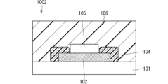
- FIG. 2 is a cross-sectional view showing stress relaxation structure 1002 according to the second embodiment.
- the stress relaxation structure 1002 includes an electronic substrate 101, a metal pattern 102, a porous layer 104, an electronic component 105, and a sealing resin 106.
- the stress relaxation structure 1002 assumes that the resist 103 covering the corners of the metal pattern 102 does not exist. In this case, when the electronic component 105 is sealed with the sealing resin 106 , stress concentrates on the corners of the metal pattern 102 . Therefore, in the stress relaxation structure 1002 , the porous layer 104 covers the corners of the metal pattern 102 .
- the stress relaxation structure 1002 since the porous layer 104 is provided so as to cover the corners of the metal pattern 102, the adhesion between the sealing resin 106 and the metal pattern 102 is enhanced, and the sealing resin from the metal pattern 102 is released. Peeling of 106 is suppressed.
- the stress relaxation structure 1002 is particularly effective when the metal pattern 102 is plated with gold or the like, which has poor adhesion to the sealing resin 106 .
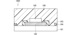
- FIG. 3 is a cross-sectional view showing stress relaxation structure 1003 according to the third embodiment.
- the stress relaxation structure 1003 differs from the stress relaxation structure 1001 of the first embodiment only in the position where the porous layer 104 is formed.
- the porous layer 104 is provided on the upper surface of the outer peripheral portion of the electronic substrate 101 .
- the peripheral portion of the electronic substrate 101 is the portion between the edge of the electronic substrate 101 and the metal pattern 102 .
- the thermal stress increases from the center to the edge, so the amount of deformation of the electronic substrate 101 due to thermal stress is the largest at the edge. Therefore, as shown in FIG. 3, by providing the porous layer 104 on the upper surface of the outer peripheral portion of the electronic substrate 101, the adhesion between the electronic substrate 101 and the sealing resin 106 is improved, and the stress relaxation structure 1003 is formed. The reliability of the electrical equipment provided with is improved.
- the porous layer 104 is provided inside the end portion of the outer peripheral portion of the electronic substrate 101 .
- the porous layer 104 may be provided on the upper surface of the edge of the electronic substrate 101 with the same effect.
- FIG. 5 is a cross-sectional view showing stress relaxation structure 1004 according to the fourth embodiment.
- the stress relaxation structure 1004 differs from the stress relaxation structure 1003 of the third embodiment only in the position where the porous layer 104 is formed.
- the porous layer 104 is provided on the upper surface of the outer peripheral portion of the electronic substrate 101 in the stress relaxing structure 1003 , but is provided on the surface layer of the outer peripheral portion of the electronic substrate 101 in the stress relaxing structure 1004 .
- the electronic component 105 In order to mount the electronic component 105 on the metal pattern 102 of the large electronic board 101, the electronic component 105 is physically fixed to the electronic board 101 by screwing or lining, flow and reflow soldering or operator soldering. It may be fixed to the electronic board 101 by soldering using a hand. In the former case, the electronic component 105 is fixed to the edge of the electronic substrate 101 , and stress associated with mechanical deformation is generated in the electronic substrate 101 . In the latter case, deformation due to the difference in thermal stress within electronic component 105 may cause cracks at the edges of electronic substrate 101 or separation of sealing resin 106 from electronic substrate 101 .
- the porous layer 104 is arranged on the surface layer of the outer peripheral portion of the electronic substrate 101 where the amount of deformation is large. It is possible to change the bending state with Therefore, even if a crack or peeling of the sealing resin 106 occurs in the outer peripheral portion of the electronic substrate 101, the effect on the mounting portion of the electronic component 105 or the metal pattern 102 can be reduced.
- the bending stress of the electronic substrate 101 is relieved by providing the porous layer 104 on at least one portion of the surface layer of the outer peripheral portion of the electronic substrate 101 . As a result, the problem of cracks in the electronic substrate 101 or peeling of the sealing resin 106 is resolved.
- the formation of the porous layer 104 itself is as described in Embodiment 1, but before that, holes for forming the porous layer 104 are formed in the surface layer of the electronic substrate 101 .
- the holes are formed by drilling or laser cutting, or chemical treatments such as etching.
- the depth of the hole is variable according to the thickness of the electronic substrate 101 and may penetrate through the electronic substrate 101 .
- the porous layer 104 is provided on the outer surface of the electronic substrate 101 inside the end portion.
- the porous layer 104 may be provided on the surface layer of the end portion of the electronic substrate 101 to achieve the same effect.
- the porous layer 104 may be provided in at least one of the locations described above. That is, the porous layer 104 includes the corners of the metal pattern 102, the corners of the resist 103 when the corners of the metal pattern 102 are covered with the resist 103, the surface layer of the outer peripheral portion of the electronic substrate 101, and the upper surface of the outer peripheral portion of the electronic substrate 101. is provided in at least one of In addition to this, the stress relaxation structures 1001 to 1004 of Embodiments 1 to 4 include the electronic substrate 101, the metal pattern 102 formed on the upper surface of the electronic substrate 101, and the metal pattern 102 formed on the upper surface of the metal pattern 102.
- An electronic component 105 and a sealing resin 106 for sealing the upper surface of the electronic substrate 101 , the metal pattern 102 , and the electronic component 105 are provided. Therefore, according to the stress relaxation structures 101-104 of Embodiments 1-4, the adhesion between the sealing resin 106 and the electronic substrate 101, the metal pattern 102, or the resist 103 can be enhanced.
- FIG. 7 is a cross-sectional view showing stress relaxation structure 1005 according to the fifth embodiment.
- Stress relief structure 1005 comprises electronic substrate 101 , metal pattern 102 , resist 103 , porous layer 104 , electronic component 105 and cap 107 .
- the porous layer 104 is provided on at least part of the surface layer of the outer periphery of the electronic substrate 101 .
- the stress relaxation structure 1005 differs from the stress relaxation structure 1004 of Embodiment 4 in that the electronic component 105 is sealed in a hollow state by the cap 107 instead of the sealing resin 106 .
- Cap 107 is made of metal, ceramic, or plastic depending on the application of electronic component 105 .
- the cap 107 has an adhesive surface that is adhered to the top surface of the outer peripheral portion of the electronic substrate 101 with an adhesive, and an internal space that accommodates the metal pattern 102 , the resist 103 , and the electronic component 105 while being adhered to the electronic substrate 101 . Prepare.
- the porous layer 104 is provided on the outer peripheral surface layer of the electronic substrate 101 . Therefore, the stress of the electronic substrate 101 is relaxed.
- the structure and material of the porous layer 104 are as described in the first embodiment. If the organic resin material used for the porous layer 104 has a Young's modulus lower than that of the adhesive that bonds the cap 107 and the electronic substrate 101, a greater stress relaxation effect can be obtained.
- the porous layer 104 is provided at a position overlapping the bonding surface of the cap 107 to the electronic substrate 101 while the cap 107 is bonded to the electronic substrate 101 . That is, the cap 107 contacts the porous layer 104 while being adhered to the electronic substrate 101 . This improves the bonding strength between the cap 107 and the electronic substrate 101 .
- the porous layer 104 secures an air passage.
- the electronic substrate material used for the electronic component 105 absorbs moisture by absorbing moisture in the air in a normal storage environment. In a device with a hollow structure, if the moisture-absorbed electronic component 105 is soldered as it is, the moisture from the electronic component 105 evaporates into the cap 107 due to the heat during soldering, and the pressure inside the cap 107 increases, causing the cap 107 to come off. can happen. However, since the porous layer 104 secures an air passage, the above troubles are suppressed.
- the porous layer 104 is provided on the outer surface of the electronic substrate 101 inside the end portion.
- the porous layer 104 may be provided on the surface layer of the end portion of the electronic substrate 101 to achieve the same effect.
- FIG. 9 is a cross-sectional view showing a stress relaxation structure 1006 according to the sixth embodiment.
- the stress relaxation structure 1006 differs from the stress relaxation structure 1005 of the fifth embodiment only in the position where the porous layer 104 is formed.
- the porous layer 104 is formed on the surface layer of the outer peripheral portion of the electronic substrate 101 in the stress relaxation structure 1005 , but is provided on the bonding surface of the cap 107 to the electronic substrate 101 in the stress relaxation structure 1006 . That is, a concave portion is provided in the bonding surface of the cap 107 to the electronic substrate 101, and the porous layer 104 is formed in this concave portion. With the cap 107 adhered to the electronic substrate 101 , the porous layer 104 is in contact with the upper surface of the peripheral portion of the electronic substrate 101 .
- porous layer 104 itself is as described in Embodiment 1, but before that, a concave portion is formed on the bonding surface of the cap 107 by die cutting.
- the porous layer 104 provided on the cap 107 does not contribute to stress relaxation, but it is possible to discharge water vapor. Therefore, it is possible to prevent the cap 107 from coming off due to increased pressure in the cap 107 . Also, depending on the material of the cap 107 , the compatibility with the adhesive may be poor and the cap 107 may easily peel off from the electronic substrate 101 . Even in such a case, the adhesiveness between the cap 107 and the electronic substrate 101 can be enhanced by selecting a material having good adhesiveness for the porous layer 104 .
- FIG. 10 is a cross-sectional view showing a stress relaxation structure 1007 according to the tenth embodiment.
- a stress relaxation structure 1007 is a structure obtained by combining the stress relaxation structure 1005 of the fifth embodiment and the stress relaxation structure 1006 of the sixth embodiment. That is, the stress relief structure 1007 comprises the porous layer 104 on both the electronic substrate 101 and the cap 107 in the contact area between the electronic substrate 101 and the cap 107 .
- the configuration of the stress relaxation structure 1007 other than the porous layer 104 is the same as the stress relaxation structures 1005 and 1006 of the fifth and sixth embodiments.
- the material and structure of the porous layer 104 provided on the electronic substrate 101 and the porous layer 104 provided on the cap 107 may be the same or different.
- the electronic component 105 can be placed in an environment close to the open air.
- Appropriate product design can be achieved by selecting the stress relaxation structures 1005 to 1007 of Embodiments 5 to 7 according to the level of airtightness required for the electronic component 105 or the degree of pressure increase in the cap 107 due to water vapor. It is possible.
- the stress relaxation structure consists of the electronic substrate 101, the metal pattern 102 formed on the upper surface of the electronic substrate 101, and the metal pattern 102 on the upper surface of the metal pattern 102.
- a cap 107 having an adhesive surface to be adhered to the upper surface of the electronic substrate 101 with an adhesive and having an internal space for accommodating the metal pattern 102 and the electronic component 105; the electronic substrate 101 and the cap and a porous layer 104 provided on at least one of the surface layer of the electronic substrate 101 and the surface layer of the cap 107 in the region where the cap 107 is bonded.
- the porous layer 104 is provided on the outer peripheral surface layer of the electronic substrate 101, the stress of the electronic substrate 101 is relieved. Moreover, since the cap 107 contacts the porous layer 104 while being adhered to the electronic substrate 101, the bonding strength between the cap 107 and the electronic substrate 101 is improved. In addition, since the porous layer 104 secures an air passage, the pressure inside the cap 107 is increased and the cap 107 is prevented from coming off.
- FIG. 11 is a cross-sectional view showing a stress relieving structure 1008 according to the eighth embodiment.
- Stress relief structure 1008 comprises electronic substrate 101 , metal pattern 102 , resist 103 and porous layer 104 .
- the stress relaxation structure 1008 does not have the electronic component 105 and the sealing resin 106 .
- porous layer 104 is formed on the surface layer of the outer peripheral portion of the electronic substrate 101 in FIG.
- the stress relaxation structure 1008 of the eighth embodiment includes the electronic substrate 101, the metal pattern 102 formed on the upper surface of the electronic substrate 101, the surface layer of the outer peripheral portion of the electronic substrate 101, and the upper surface of the outer peripheral portion of the electronic substrate 101. and a porous layer 104 provided on at least one of the above.
- the provision of the porous layer 104 on the outer peripheral portion of the electronic substrate 101 reduces the thermal stress when mounting the electronic component on the metal pattern 102.
- the warpage of the electronic substrate 101 due to is alleviated.
- the outer peripheral portion of the electronic board 101 is physically fixed by screwing or caulking, the stress of the electronic board 101 is relieved.
- the porous layer 104 is arranged on the surface layer of the outer peripheral portion of the electronic substrate 101 where the amount of deformation is large. It is possible to change the bending state with Therefore, even if a crack occurs in the outer peripheral portion of the electronic substrate 101, it is possible to reduce the influence on the mounting portion of the electronic component or the metal pattern 102.
- FIG. The bending stress of the electronic substrate 101 is relieved by providing the porous layer 104 on at least one portion of the surface layer of the outer peripheral portion of the electronic substrate 101 . As a result, cracks in the electronic substrate 101 are suppressed.
- the method for forming the porous layer 104 on the outer peripheral surface layer of the electronic substrate 101 is as described in the first and fourth embodiments.
Landscapes
- Engineering & Computer Science (AREA)
- Manufacturing & Machinery (AREA)
- Microelectronics & Electronic Packaging (AREA)
- Non-Metallic Protective Coatings For Printed Circuits (AREA)
- Structures Or Materials For Encapsulating Or Coating Semiconductor Devices Or Solid State Devices (AREA)
Priority Applications (5)
| Application Number | Priority Date | Filing Date | Title |
|---|---|---|---|
| JP2021576940A JP7118298B1 (ja) | 2021-08-19 | 2021-08-19 | 応力緩和構造および応力緩和構造の製造方法 |
| PCT/JP2021/030314 WO2023021643A1 (ja) | 2021-08-19 | 2021-08-19 | 応力緩和構造 |
| DE112021008123.3T DE112021008123T5 (de) | 2021-08-19 | 2021-08-19 | Spannungsentlastungsstruktur |
| US18/576,116 US20240243023A1 (en) | 2021-08-19 | 2021-08-19 | Stress relief structure, electronic component and method of manufacturing stress relief structure |
| CN202180101444.2A CN117813682A (zh) | 2021-08-19 | 2021-08-19 | 应力缓和结构 |
Applications Claiming Priority (1)
| Application Number | Priority Date | Filing Date | Title |
|---|---|---|---|
| PCT/JP2021/030314 WO2023021643A1 (ja) | 2021-08-19 | 2021-08-19 | 応力緩和構造 |
Publications (1)
| Publication Number | Publication Date |
|---|---|
| WO2023021643A1 true WO2023021643A1 (ja) | 2023-02-23 |
Family
ID=82847600
Family Applications (1)
| Application Number | Title | Priority Date | Filing Date |
|---|---|---|---|
| PCT/JP2021/030314 Ceased WO2023021643A1 (ja) | 2021-08-19 | 2021-08-19 | 応力緩和構造 |
Country Status (5)
| Country | Link |
|---|---|
| US (1) | US20240243023A1 (https=) |
| JP (1) | JP7118298B1 (https=) |
| CN (1) | CN117813682A (https=) |
| DE (1) | DE112021008123T5 (https=) |
| WO (1) | WO2023021643A1 (https=) |
Citations (4)
| Publication number | Priority date | Publication date | Assignee | Title |
|---|---|---|---|---|
| JP2008277954A (ja) * | 2007-04-26 | 2008-11-13 | Fujitsu Media Device Kk | パッケージデバイス |
| JP2016152386A (ja) * | 2015-02-19 | 2016-08-22 | 三菱マテリアル株式会社 | パワーモジュール用基板及びパワーモジュール |
| WO2018159696A1 (ja) * | 2017-03-03 | 2018-09-07 | 浩明 中弥 | 光熱変換基板を備えた熱電変換モジュール |
| JP2021077781A (ja) * | 2019-11-11 | 2021-05-20 | 株式会社ディスコ | チャックテーブルおよびチャックテーブルの製造方法 |
Family Cites Families (4)
| Publication number | Priority date | Publication date | Assignee | Title |
|---|---|---|---|---|
| JP2001085802A (ja) * | 1999-09-16 | 2001-03-30 | Hitachi Cable Ltd | 配線基板及びそれを用いた電子装置及びその製造方法 |
| JP2006277954A (ja) * | 2005-03-28 | 2006-10-12 | Jfe Steel Kk | 断路端子台 |
| JP2008241641A (ja) | 2007-03-29 | 2008-10-09 | Sumitomo Electric Ind Ltd | インターポーザおよびその製造方法 |
| JP6205914B2 (ja) | 2013-07-08 | 2017-10-04 | 三菱電機株式会社 | モジュール構造 |
-
2021
- 2021-08-19 US US18/576,116 patent/US20240243023A1/en active Pending
- 2021-08-19 WO PCT/JP2021/030314 patent/WO2023021643A1/ja not_active Ceased
- 2021-08-19 JP JP2021576940A patent/JP7118298B1/ja active Active
- 2021-08-19 DE DE112021008123.3T patent/DE112021008123T5/de active Pending
- 2021-08-19 CN CN202180101444.2A patent/CN117813682A/zh active Pending
Patent Citations (4)
| Publication number | Priority date | Publication date | Assignee | Title |
|---|---|---|---|---|
| JP2008277954A (ja) * | 2007-04-26 | 2008-11-13 | Fujitsu Media Device Kk | パッケージデバイス |
| JP2016152386A (ja) * | 2015-02-19 | 2016-08-22 | 三菱マテリアル株式会社 | パワーモジュール用基板及びパワーモジュール |
| WO2018159696A1 (ja) * | 2017-03-03 | 2018-09-07 | 浩明 中弥 | 光熱変換基板を備えた熱電変換モジュール |
| JP2021077781A (ja) * | 2019-11-11 | 2021-05-20 | 株式会社ディスコ | チャックテーブルおよびチャックテーブルの製造方法 |
Also Published As
| Publication number | Publication date |
|---|---|
| JP7118298B1 (ja) | 2022-08-15 |
| US20240243023A1 (en) | 2024-07-18 |
| JPWO2023021643A1 (https=) | 2023-02-23 |
| CN117813682A (zh) | 2024-04-02 |
| DE112021008123T5 (de) | 2024-05-29 |
Similar Documents
| Publication | Publication Date | Title |
|---|---|---|
| US8212353B1 (en) | Structure and assembly procedure for low stress thin die flip chip packages designed for low-K Si and thin core substrate | |
| US6949404B1 (en) | Flip chip package with warpage control | |
| JP2008172172A (ja) | 電子制御装置及びその製造方法 | |
| KR20050118694A (ko) | 얇은 언더필 및 두꺼운 솔더 마스크를 가지는 플립-칩어셈블리 | |
| WO2008057896A2 (en) | Multi-component electronic package with planarized embedded-components substrate | |
| US20120119358A1 (en) | Semicondiuctor package substrate and method for manufacturing the same | |
| CN107039357A (zh) | 芯片保护封壳和方法 | |
| US7998797B2 (en) | Semiconductor device | |
| JP7118298B1 (ja) | 応力緩和構造および応力緩和構造の製造方法 | |
| KR100608610B1 (ko) | 인쇄회로기판과, 그의 제조 방법 및 그를 이용한 반도체패키지 | |
| JP6467775B2 (ja) | 部品内蔵基板の製造方法 | |
| US7365434B2 (en) | Semiconductor device and manufacturing method for the same | |
| CN102655715B (zh) | 柔性印刷电路板及其制造方法 | |
| US6677185B2 (en) | Method of affixing a heat sink to a substrate and package thereof | |
| US6707163B2 (en) | Method of eliminating uncontrolled voids in sheet adhesive layer | |
| JP4830861B2 (ja) | 接合構造体の製造方法 | |
| JP5556007B2 (ja) | 電子装置 | |
| JP5146358B2 (ja) | 電子装置 | |
| KR20140083512A (ko) | 패키지 기판 및 그 제조방법 | |
| CN111508903A (zh) | 电子装置的封装基板结构及其制造方法 | |
| KR20030085449A (ko) | 개량된 플립 칩 패키지 | |
| KR100720918B1 (ko) | 이형복합 피씨비 제조방법과 그 피씨비 기판 | |
| TWI864971B (zh) | 電子組件及其製造方法 | |
| JP7797381B2 (ja) | リッドレスbgaパッケージにおける複数列の表面実装コンポーネントのコンフォーマルコーティングプロセス及びそれによって製造された製品 | |
| US11270894B2 (en) | Manufacturing method for semiconductor package with cantilever pads |
Legal Events
| Date | Code | Title | Description |
|---|---|---|---|
| ENP | Entry into the national phase |
Ref document number: 2021576940 Country of ref document: JP Kind code of ref document: A |
|
| 121 | Ep: the epo has been informed by wipo that ep was designated in this application |
Ref document number: 21954216 Country of ref document: EP Kind code of ref document: A1 |
|
| WWE | Wipo information: entry into national phase |
Ref document number: 18576116 Country of ref document: US |
|
| WWE | Wipo information: entry into national phase |
Ref document number: 202180101444.2 Country of ref document: CN |
|
| 122 | Ep: pct application non-entry in european phase |
Ref document number: 21954216 Country of ref document: EP Kind code of ref document: A1 |