WO2023013506A1 - 処理方法及びプラズマ処理装置 - Google Patents
処理方法及びプラズマ処理装置 Download PDFInfo
- Publication number
- WO2023013506A1 WO2023013506A1 PCT/JP2022/029016 JP2022029016W WO2023013506A1 WO 2023013506 A1 WO2023013506 A1 WO 2023013506A1 JP 2022029016 W JP2022029016 W JP 2022029016W WO 2023013506 A1 WO2023013506 A1 WO 2023013506A1
- Authority
- WO
- WIPO (PCT)
- Prior art keywords
- heat transfer
- wafer
- transfer layer
- mounting surface
- plasma processing
- Prior art date
- Legal status (The legal status is an assumption and is not a legal conclusion. Google has not performed a legal analysis and makes no representation as to the accuracy of the status listed.)
- Ceased
Links
Images





Classifications
-
- H—ELECTRICITY
- H10—SEMICONDUCTOR DEVICES; ELECTRIC SOLID-STATE DEVICES NOT OTHERWISE PROVIDED FOR
- H10P—GENERIC PROCESSES OR APPARATUS FOR THE MANUFACTURE OR TREATMENT OF DEVICES COVERED BY CLASS H10
- H10P72/00—Handling or holding of wafers, substrates or devices during manufacture or treatment thereof
- H10P72/04—Apparatus for manufacture or treatment
- H10P72/0431—Apparatus for thermal treatment
- H10P72/0432—Apparatus for thermal treatment mainly by conduction
-
- H—ELECTRICITY
- H01—ELECTRIC ELEMENTS
- H01J—ELECTRIC DISCHARGE TUBES OR DISCHARGE LAMPS
- H01J37/00—Discharge tubes with provision for introducing objects or material to be exposed to the discharge, e.g. for the purpose of examination or processing thereof
- H01J37/32—Gas-filled discharge tubes
- H01J37/32431—Constructional details of the reactor
- H01J37/32715—Workpiece holder
- H01J37/32724—Temperature
-
- C—CHEMISTRY; METALLURGY
- C23—COATING METALLIC MATERIAL; COATING MATERIAL WITH METALLIC MATERIAL; CHEMICAL SURFACE TREATMENT; DIFFUSION TREATMENT OF METALLIC MATERIAL; COATING BY VACUUM EVAPORATION, BY SPUTTERING, BY ION IMPLANTATION OR BY CHEMICAL VAPOUR DEPOSITION, IN GENERAL; INHIBITING CORROSION OF METALLIC MATERIAL OR INCRUSTATION IN GENERAL
- C23C—COATING METALLIC MATERIAL; COATING MATERIAL WITH METALLIC MATERIAL; SURFACE TREATMENT OF METALLIC MATERIAL BY DIFFUSION INTO THE SURFACE, BY CHEMICAL CONVERSION OR SUBSTITUTION; COATING BY VACUUM EVAPORATION, BY SPUTTERING, BY ION IMPLANTATION OR BY CHEMICAL VAPOUR DEPOSITION, IN GENERAL
- C23C16/00—Chemical coating by decomposition of gaseous compounds, without leaving reaction products of surface material in the coating, i.e. chemical vapour deposition [CVD] processes
- C23C16/44—Chemical coating by decomposition of gaseous compounds, without leaving reaction products of surface material in the coating, i.e. chemical vapour deposition [CVD] processes characterised by the method of coating
- C23C16/50—Chemical coating by decomposition of gaseous compounds, without leaving reaction products of surface material in the coating, i.e. chemical vapour deposition [CVD] processes characterised by the method of coating using electric discharges
-
- H—ELECTRICITY
- H01—ELECTRIC ELEMENTS
- H01J—ELECTRIC DISCHARGE TUBES OR DISCHARGE LAMPS
- H01J37/00—Discharge tubes with provision for introducing objects or material to be exposed to the discharge, e.g. for the purpose of examination or processing thereof
- H01J37/32—Gas-filled discharge tubes
- H01J37/32431—Constructional details of the reactor
- H01J37/3244—Gas supply means
-
- H—ELECTRICITY
- H01—ELECTRIC ELEMENTS
- H01J—ELECTRIC DISCHARGE TUBES OR DISCHARGE LAMPS
- H01J37/00—Discharge tubes with provision for introducing objects or material to be exposed to the discharge, e.g. for the purpose of examination or processing thereof
- H01J37/32—Gas-filled discharge tubes
- H01J37/32431—Constructional details of the reactor
- H01J37/32623—Mechanical discharge control means
- H01J37/32642—Focus rings
-
- H—ELECTRICITY
- H10—SEMICONDUCTOR DEVICES; ELECTRIC SOLID-STATE DEVICES NOT OTHERWISE PROVIDED FOR
- H10P—GENERIC PROCESSES OR APPARATUS FOR THE MANUFACTURE OR TREATMENT OF DEVICES COVERED BY CLASS H10
- H10P14/00—Formation of materials, e.g. in the shape of layers or pillars
- H10P14/20—Formation of materials, e.g. in the shape of layers or pillars of semiconductor materials
- H10P14/29—Formation of materials, e.g. in the shape of layers or pillars of semiconductor materials characterised by the substrates
-
- H—ELECTRICITY
- H10—SEMICONDUCTOR DEVICES; ELECTRIC SOLID-STATE DEVICES NOT OTHERWISE PROVIDED FOR
- H10P—GENERIC PROCESSES OR APPARATUS FOR THE MANUFACTURE OR TREATMENT OF DEVICES COVERED BY CLASS H10
- H10P14/00—Formation of materials, e.g. in the shape of layers or pillars
- H10P14/60—Formation of materials, e.g. in the shape of layers or pillars of insulating materials
-
- H—ELECTRICITY
- H10—SEMICONDUCTOR DEVICES; ELECTRIC SOLID-STATE DEVICES NOT OTHERWISE PROVIDED FOR
- H10P—GENERIC PROCESSES OR APPARATUS FOR THE MANUFACTURE OR TREATMENT OF DEVICES COVERED BY CLASS H10
- H10P50/00—Etching of wafers, substrates or parts of devices
- H10P50/20—Dry etching; Plasma etching; Reactive-ion etching
- H10P50/24—Dry etching; Plasma etching; Reactive-ion etching of semiconductor materials
- H10P50/242—Dry etching; Plasma etching; Reactive-ion etching of semiconductor materials of Group IV materials
-
- H—ELECTRICITY
- H10—SEMICONDUCTOR DEVICES; ELECTRIC SOLID-STATE DEVICES NOT OTHERWISE PROVIDED FOR
- H10P—GENERIC PROCESSES OR APPARATUS FOR THE MANUFACTURE OR TREATMENT OF DEVICES COVERED BY CLASS H10
- H10P72/00—Handling or holding of wafers, substrates or devices during manufacture or treatment thereof
- H10P72/70—Handling or holding of wafers, substrates or devices during manufacture or treatment thereof for supporting or gripping
-
- H—ELECTRICITY
- H10—SEMICONDUCTOR DEVICES; ELECTRIC SOLID-STATE DEVICES NOT OTHERWISE PROVIDED FOR
- H10P—GENERIC PROCESSES OR APPARATUS FOR THE MANUFACTURE OR TREATMENT OF DEVICES COVERED BY CLASS H10
- H10P72/00—Handling or holding of wafers, substrates or devices during manufacture or treatment thereof
- H10P72/70—Handling or holding of wafers, substrates or devices during manufacture or treatment thereof for supporting or gripping
- H10P72/72—Handling or holding of wafers, substrates or devices during manufacture or treatment thereof for supporting or gripping using electrostatic chucks
-
- H—ELECTRICITY
- H10—SEMICONDUCTOR DEVICES; ELECTRIC SOLID-STATE DEVICES NOT OTHERWISE PROVIDED FOR
- H10P—GENERIC PROCESSES OR APPARATUS FOR THE MANUFACTURE OR TREATMENT OF DEVICES COVERED BY CLASS H10
- H10P72/00—Handling or holding of wafers, substrates or devices during manufacture or treatment thereof
- H10P72/70—Handling or holding of wafers, substrates or devices during manufacture or treatment thereof for supporting or gripping
- H10P72/76—Handling or holding of wafers, substrates or devices during manufacture or treatment thereof for supporting or gripping using mechanical means, e.g. clamps or pinches
- H10P72/7604—Handling or holding of wafers, substrates or devices during manufacture or treatment thereof for supporting or gripping using mechanical means, e.g. clamps or pinches the wafers being placed on a susceptor, stage or support
- H10P72/7611—Handling or holding of wafers, substrates or devices during manufacture or treatment thereof for supporting or gripping using mechanical means, e.g. clamps or pinches the wafers being placed on a susceptor, stage or support characterised by edge profile or support profile
-
- H—ELECTRICITY
- H10—SEMICONDUCTOR DEVICES; ELECTRIC SOLID-STATE DEVICES NOT OTHERWISE PROVIDED FOR
- H10P—GENERIC PROCESSES OR APPARATUS FOR THE MANUFACTURE OR TREATMENT OF DEVICES COVERED BY CLASS H10
- H10P72/00—Handling or holding of wafers, substrates or devices during manufacture or treatment thereof
- H10P72/70—Handling or holding of wafers, substrates or devices during manufacture or treatment thereof for supporting or gripping
- H10P72/76—Handling or holding of wafers, substrates or devices during manufacture or treatment thereof for supporting or gripping using mechanical means, e.g. clamps or pinches
- H10P72/7604—Handling or holding of wafers, substrates or devices during manufacture or treatment thereof for supporting or gripping using mechanical means, e.g. clamps or pinches the wafers being placed on a susceptor, stage or support
- H10P72/7612—Handling or holding of wafers, substrates or devices during manufacture or treatment thereof for supporting or gripping using mechanical means, e.g. clamps or pinches the wafers being placed on a susceptor, stage or support characterised by lifting arrangements, e.g. lift pins
-
- H—ELECTRICITY
- H10—SEMICONDUCTOR DEVICES; ELECTRIC SOLID-STATE DEVICES NOT OTHERWISE PROVIDED FOR
- H10P—GENERIC PROCESSES OR APPARATUS FOR THE MANUFACTURE OR TREATMENT OF DEVICES COVERED BY CLASS H10
- H10P72/00—Handling or holding of wafers, substrates or devices during manufacture or treatment thereof
- H10P72/70—Handling or holding of wafers, substrates or devices during manufacture or treatment thereof for supporting or gripping
- H10P72/76—Handling or holding of wafers, substrates or devices during manufacture or treatment thereof for supporting or gripping using mechanical means, e.g. clamps or pinches
- H10P72/7604—Handling or holding of wafers, substrates or devices during manufacture or treatment thereof for supporting or gripping using mechanical means, e.g. clamps or pinches the wafers being placed on a susceptor, stage or support
- H10P72/7624—Handling or holding of wafers, substrates or devices during manufacture or treatment thereof for supporting or gripping using mechanical means, e.g. clamps or pinches the wafers being placed on a susceptor, stage or support characterised by the mechanical construction of the susceptor, stage or support
Definitions
- the present disclosure relates to a processing method and a plasma processing apparatus.
- Patent Document 1 discloses a substrate provided with a mounting table having a mounting surface on which a substrate is mounted and provided with a gas supply pipe for supplying a heat transfer gas to a gap between the substrate and the mounting surface.
- a processing device is disclosed.
- the technology according to the present disclosure efficiently adjusts the temperature of an object to be temperature-controlled during plasma processing.
- One aspect of the present disclosure is a processing method for performing plasma processing on a substrate, which includes the steps of placing a temperature adjustment target on a placement surface of a substrate support part in a processing container configured to be depressurized; forming on the mounting surface of the substrate support portion a deformable heat transfer layer for the object to be temperature-controlled, which is composed of at least one of a liquid layer and a deformable solid layer; and performing plasma processing on the substrate on the mounting surface on which the heat transfer layer is formed.
- FIG. 1 is a plan view showing an outline of a configuration of a plasma processing system including processing modules as a plasma processing apparatus according to a first embodiment
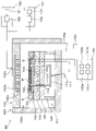
- FIG. 1 is a vertical cross-sectional view showing an outline of a configuration of a processing module as a plasma processing apparatus according to a first embodiment
- FIG. 3 is a flowchart for explaining an example of wafer processing performed using the processing module of FIG. 2; 3 illustrates the state of the processing module of FIG. 2 during wafer processing; FIG. 3 illustrates the state of the processing module of FIG. 2 during wafer processing; FIG. 3 illustrates the state of the processing module of FIG. 2 during wafer processing; FIG. 3 illustrates the state of the processing module of FIG. 2 during wafer processing; FIG. 3 illustrates the state of the processing module of FIG. 2 during wafer processing; FIG. 3 illustrates the state of the processing module of FIG. 3 illustrates the state of the processing module of FIG.
- FIG. 4 is a diagram for explaining another example of the supply form of the raw material gas;
- FIG. 4 is a diagram for explaining another example of the supply form of the raw material gas;
- FIG. 4 is a diagram for explaining another example of the supply form of the raw material gas;
- FIG. 4 is a diagram for explaining another example of the supply form of the raw material gas;
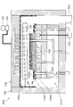
- FIG. 10 is a diagram for explaining another example of the state inside the processing container when forming the heat transfer layer;
- It is a longitudinal cross-sectional view showing an outline of a configuration of a processing module as a plasma processing apparatus according to a second embodiment.
- 15 is a flowchart for explaining an example of wafer processing performed using the processing module of FIG. 14; 15 illustrates the state of the processing module of FIG.
- FIG. 15 illustrates the state of the processing module of FIG. 14 during wafer processing;
- FIG. 15 illustrates the state of the processing module of FIG. 14 during wafer processing;
- FIG. 15 illustrates the state of the processing module of FIG. 14 during wafer processing;
- FIG. It is a figure which shows the example of a groove
- FIG. 11 is a vertical cross-sectional view showing the outline of the configuration of a processing module as a plasma processing apparatus according to a third embodiment;
- FIG. 11 is a vertical cross-sectional view showing the outline of the configuration of a processing module as a plasma processing apparatus according to a fourth embodiment;
- FIG. 11 is a plan view showing the outline of the configuration of a plasma processing system including processing modules as a plasma processing apparatus according to a fifth embodiment;
- FIG. 11 is a vertical cross-sectional view showing the outline of the configuration of a processing module as a plasma processing apparatus according to a fifth embodiment;
- 26 is a flowchart for explaining an example of wafer processing performed using the processing module of FIG. 25;
- 26 illustrates the state of the processing module of FIG. 25 during wafer processing;
- FIG. 26 illustrates the state of the processing module of FIG. 25 during wafer processing;
- FIG. 26 illustrates the state of the processing module of FIG. 25 during wafer processing;
- FIG. 26 illustrates the state of the processing module of FIG. 25 during wafer processing;
- FIG. 12 is a vertical cross-sectional view showing the outline of the configuration of a processing module as a plasma processing apparatus according to a sixth embodiment
- FIG. 12 is a vertical cross-sectional view showing the outline of the configuration of a processing module as a plasma processing apparatus according to a sixth embodiment
- 33 is a flowchart for explaining an example of wafer processing performed using the processing modules of FIGS. 31 and 32
- FIG. 33 illustrates the processing module of FIGS. 31 and 32 during wafer processing
- FIG. 33 illustrates the processing module of FIGS. 31 and 32 during wafer processing
- FIG. 33 illustrates the processing module of FIGS. 31 and 32 during wafer processing
- FIG. 33 illustrates the processing module of FIGS. 31 and 32 during wafer processing
- plasma processing such as etching and film formation is performed using plasma on substrates such as semiconductor wafers (hereinafter referred to as "wafers").
- substrates such as semiconductor wafers (hereinafter referred to as "wafers").
- Plasma processing is performed with a substrate placed on a substrate support table in a depressurized processing container.
- annular member in plan view that is, an edge ring is provided on the substrate support so as to surround the periphery of the substrate on the substrate support. may be placed on
- the temperature of the substrate support is adjusted during the plasma processing, and the temperature of the substrate is adjusted via this substrate support.
- temperature control of the edge ring is also important because the temperature of the edge ring affects the plasma processing result of the substrate periphery.
- the temperature of the edge ring is also adjusted via the substrate support.
- a heat transfer gas such as He gas is supplied between the substrate support and the substrate and the edge ring so that the temperatures of the substrate and the edge ring are efficiently adjusted through the substrate support.
- the temperature of at least one of the substrate and the edge ring may not be sufficiently adjusted even if the heat transfer gas is used as described above.
- the technology according to the present disclosure efficiently adjusts the temperature of the object to be temperature-adjusted, which is at least one of the substrate and the edge ring, during plasma processing.
- FIG. 1 is a plan view showing the schematic configuration of a plasma processing system including processing modules as a plasma processing apparatus according to the first embodiment.
- the atmospheric part 10 includes an atmospheric module that performs desired processing on a wafer W as a substrate under atmospheric pressure.
- the decompression unit 11 includes a processing module 60 that performs desired processing on the wafer W under a decompressed atmosphere (vacuum atmosphere).
- the load lock modules 20 and 21 are provided to connect the loader module 30 included in the atmosphere section 10 and the transfer module 50 included in the decompression section 11 via gate valves (not shown).
- the load lock modules 20, 21 are configured to hold the wafer W temporarily. Further, the load lock modules 20 and 21 are configured so that the inside can be switched between an atmospheric pressure atmosphere and a reduced pressure atmosphere.
- the atmospheric part 10 has a loader module 30 having a transport mechanism 40, which will be described later, and a load port 32 on which a FOUP (FOUP: Front Opening Unified Pod) 31 is placed.
- the FOUP 31 is capable of storing a plurality of wafers W.
- FIG. An orienter module (not shown) for adjusting the horizontal direction of the wafer W, a buffer module (not shown) for temporarily storing a plurality of wafers W, and the like are connected to the loader module 30. good.
- the loader module 30 has a rectangular housing, and the inside of the housing is maintained at atmospheric pressure.
- a plurality of, for example, five load ports 32 are arranged side by side on one side surface that constitutes the long side of the housing of the loader module 30 .
- Load-lock modules 20 and 21 are arranged side by side on the other side surface constituting the long side of the housing of the loader module 30 .
- a transport mechanism 40 capable of transporting the wafer W is provided inside the housing of the loader module 30 .
- the transfer mechanism 40 has a transfer arm 41 that supports the wafer W during transfer, a turntable 42 that rotatably supports the transfer arm 41, and a base 43 on which the turntable 42 is mounted.
- a guide rail 44 extending in the longitudinal direction of the loader module 30 is provided inside the loader module 30 .
- the base 43 is provided on guide rails 44 , and the transport mechanism 40 is configured to be movable along the guide rails 44 .
- the decompression unit 11 has a transfer module 50 that transfers the wafer W, and a processing module 60 as a plasma processing apparatus that performs plasma processing on the wafer W transferred from the transfer module 50 .
- the interiors of the transfer module 50 and the processing module 60 (specifically, the interiors of the depressurized transfer chamber 51 and the plasma processing chamber 100 to be described later) are maintained in a depressurized atmosphere.
- a plurality of, for example eight, processing modules 60 are provided for one transfer module 50 .
- the transfer module 50 includes a reduced pressure transfer chamber 51 having a polygonal (pentagonal in the illustrated example) housing, and the reduced pressure transfer chamber 51 is connected to the load lock modules 20 and 21 .
- the transfer module 50 transfers the wafer W loaded into the load lock module 20 to one processing module 60, and transfers the wafer W subjected to the desired plasma processing in the processing module 60 through the load lock module 21. It is carried out to the atmospheric part 10 .
- the processing module 60 performs plasma processing such as etching and film formation on the wafer W, for example. Also, the processing module 60 is connected to the transfer module 50 via a gate valve 61 . The configuration of this processing module 60 will be described later.
- a transfer mechanism 70 configured to transfer the wafer W is provided inside the depressurized transfer chamber 51 of the transfer module 50 .
- the transport mechanism 70 includes a transport arm 71 that supports the wafer W during transport, a turntable 72 that rotatably supports the transport arm 71, and a base 73 on which the turntable 72 is mounted. have.
- a guide rail 74 extending in the longitudinal direction of the transfer module 50 is provided inside the reduced-pressure transfer chamber 51 of the transfer module 50 .
- the base 73 is provided on guide rails 74 , and the transport mechanism 70 is configured to be movable along the guide rails 74 .
- the transfer arm 71 receives the wafer W held in the load lock module 20 and carries it into the processing module 60 . Also, the transfer arm 71 receives the wafer held in the processing module 60 and unloads it to the load lock module 21 .
- controller 80 processes computer-executable instructions that cause plasma processing system 1 to perform various operations described in this disclosure. Controller 80 may be configured to control each of the other elements of plasma processing system 1 to perform the various processes described herein. In one embodiment, some or all of controller 80 may be included in other elements of plasma processing system 1 . In one embodiment, controller 80 also processes computer-executable instructions that cause processing module 60 to perform various steps described in this disclosure. Controller 80 may be configured to control each of the other elements of processing module 60 to perform the various steps described herein. In one embodiment, some or all of controller 80 may be included in other elements of processing module 60 . The controller 80 may include a computer 90, for example.
- the computer 90 may include a processing unit (CPU: Central Processing Unit) 91, a storage unit 92, and a communication interface 93, for example.
- the processing unit 91 can be configured to perform various control operations based on programs stored in the storage unit 92 .
- the storage unit 92 may include RAM (Random Access Memory), ROM (Read Only Memory), HDD (Hard Disk Drive), SSD (Solid State Drive), or a combination thereof.
- the communication interface 93 may communicate with other elements of the plasma processing system 1 via a communication line such as a LAN (Local Area Network).
- the wafer W is taken out from the desired FOUP 31 and loaded into the load lock module 20 by the transport mechanism 40 . After that, the inside of the load lock module 20 is sealed and the pressure is reduced. After that, the inside of the load lock module 20 and the inside of the transfer module 50 are communicated.
- the wafer W is held by the transport mechanism 70 and transported from the load lock module 20 to the transfer module 50 .
- the gate valve 61 is opened, and the wafer W is carried into the desired processing module 60 by the transfer mechanism 70 . After that, the gate valve 61 is closed, and the wafer W is subjected to desired processing in the processing module 60 .
- the processing performed on the wafer W in this processing module 60 will be described later.
- the gate valve 61 is opened, and the wafer W is unloaded from the processing module 60 by the transport mechanism 70 . After that, the gate valve 61 is closed.
- the wafer W is loaded into the load lock module 21 by the transport mechanism 70 .
- the inside of the load lock module 21 is sealed and opened to the atmosphere. After that, the inside of the load lock module 21 and the inside of the loader module 30 are communicated with each other.
- the wafer W is held by the transfer mechanism 40 and returned from the load lock module 21 via the loader module 30 to the desired FOUP 31 to be accommodated.
- a series of wafer processing in the plasma processing system 1 is now completed.
- FIG. 2 is a vertical cross-sectional view showing an outline of the configuration of the processing module 60. As shown in FIG.
- the processing module 60 includes a plasma processing chamber 100 as a processing container, gas supply units 120 and 130, an RF (Radio Frequency) power supply unit 140, and an exhaust system 150. Further, the processing module 60 includes a wafer support 101 and an upper electrode 102 as substrate supports.
- the wafer support table 101 is arranged in the lower region of the plasma processing space 100s in the plasma processing chamber 100 configured to be depressurized.
- Upper electrode 102 is arranged above wafer support 101 . Also, the upper electrode 102 may function as part of a wall that defines the plasma processing space 100 s , more specifically, as part of the ceiling of the plasma processing chamber 100 .
- the wafer support 101 is configured to support the wafer W in the plasma processing space 100s.
- the wafer support 101 includes a lower electrode 103, an electrostatic chuck 104, an insulator 105, legs 106, and a lifter 107 is provided.
- the wafer support table 101 also includes a temperature adjustment unit configured to adjust the temperature of the electrostatic chuck 104 (for example, the temperature of the central upper surface 1041 ).
- the temperature adjuster includes, for example, heaters, channels, or a combination thereof.
- a temperature control fluid such as a refrigerant or a heat transfer gas flows through the flow path.
- the lower electrode 103 is made of a conductive material such as aluminum, and fixed to the insulator 105 .
- a flow path 108 for the temperature control fluid is formed, which constitutes a part of the temperature control section.
- a temperature control fluid is supplied to the flow path 108 from, for example, a chiller unit (not shown) provided outside the plasma processing chamber 100 .
- the temperature-controlled fluid supplied to the flow path 108 is returned to the chiller unit.
- the electrostatic chuck 104, the wafer W placed on the electrostatic chuck 104, and the edge ring E are cooled to a predetermined temperature by circulating low-temperature brine as a temperature control fluid in the flow path 108. can be done.
- the electrostatic chuck 104, the wafer W placed on the electrostatic chuck 104, and the edge ring E are heated to a predetermined temperature. can do.
- the electrostatic chuck 104 is a member configured to attract and hold the wafer W by electrostatic force, and is provided on the lower electrode 103 .
- the electrostatic chuck 104 is formed such that the upper surface of the central portion is higher than the upper surface of the peripheral portion.
- the upper surface 104 1 of the central portion of the electrostatic chuck 104 serves as a wafer mounting surface on which the wafer W is mounted, and the upper surface 104 2 of the peripheral portion of the electrostatic chuck 104 serves as a ring mounting surface on which the edge ring E is mounted. face.
- the edge ring E is an annular member arranged adjacent to the wafer W so as to surround the wafer W placed on the upper surface 1041 of the central portion of the electrostatic chuck 104 .
- the electrostatic chuck 104 is an example of a fixing portion that fixes the wafer W to the upper surface 104 1 at the center of the electrostatic chuck 104 , that is, the wafer mounting surface.
- An electrode 109 is provided in the center of the electrostatic chuck 104 .
- a DC voltage is applied to the electrode 109 from a DC power supply (not shown).
- the wafer W is attracted and held on the upper surface 1041 at the center of the electrostatic chuck 104 by the electrostatic force generated thereby.
- the electrostatic chuck 104 is configured to be able to attract and hold the edge ring E by electrostatic force, and is provided with an electrode (not shown) for holding the edge ring E on the wafer support 101 by electrostatic attraction.
- a heat transfer gas such as He gas is supplied to the upper surface 1042 of the peripheral portion of the electrostatic chuck 104 to the rear surface of the edge ring E placed on the upper surface 1042 .
- a feed hole (not shown) is formed.
- a heat transfer gas is supplied from a gas supply section (not shown) through the gas supply holes.
- a gas supply may include one or more gas sources and one or more pressure controllers.
- the gas supply is configured to supply heat transfer gas, for example from a gas source, to the gas supply holes via a pressure controller.
- the central portion of the electrostatic chuck 104 is formed, for example, to have a smaller diameter than the diameter of the wafer W, and the wafer W is placed on the upper surface (hereinafter referred to as wafer mounting surface) 104 1 of the central portion of the electrostatic chuck 104 .
- wafer mounting surface 104 1 of the central portion of the electrostatic chuck 104 .
- the peripheral edge of the wafer W protrudes from the central portion of the electrostatic chuck 104 .
- the edge ring E has, for example, a step formed in its upper portion, and the upper surface of the outer peripheral portion is formed higher than the upper surface of the inner peripheral portion.
- the inner peripheral portion of the edge ring E is formed so as to go under the peripheral portion of the wafer W projecting from the central portion of the electrostatic chuck 104 .
- a heater (specifically, a resistance heating element) forming part of the temperature control mechanism may be provided inside the electrostatic chuck 104.
- the electrostatic chuck 104 has, for example, a configuration in which a wafer attracting electrode 109 and an edge ring attracting electrode are sandwiched between insulating materials made of an insulating material, and a heater is embedded.
- the central portion of the electrostatic chuck 104 provided with the electrode 109 for attracting the wafer and the peripheral portion of the electrostatic chuck 104 provided with the electrode for attracting the edge ring may be integrally formed. , may be separate.
- the insulator 105 is a disk-shaped member made of ceramic or the like, to which the lower electrode 103 is fixed.
- the insulator 105 is formed to have the same diameter as the lower electrode 103, for example.
- the leg 106 is a cylindrical member made of ceramic or the like, and supports the electrostatic chuck 104 via the lower electrode 103 and insulator 105 .
- the legs 106 are formed, for example, to have an outer diameter equal to that of the insulator 105 and support the periphery of the insulator 105 .
- the lifter 107 is a lifting member that moves up and down with respect to the wafer mounting surface 1041 of the electrostatic chuck 104, and is formed in a columnar shape, for example.
- the lifter 107 can support the wafer W with its upper end protruding from the wafer mounting surface 1041 when lifted.
- the lifter 107 can transfer the wafer W between the electrostatic chuck 104 and the transfer arm 71 of the transfer mechanism 70 .
- Three or more lifters 107 are provided at intervals, and are provided so as to extend in the vertical direction.
- Each lifter 107 is connected to a support member 110 that supports the lifter 107 . Further, the support member 110 is connected to a drive unit 111 that generates driving force for raising and lowering the support member 110 and raises and lowers the plurality of lifters 107 .
- the drive unit 111 has, for example, a motor (not shown) as a drive source that generates the drive force.
- the lifter 107 is inserted through an insertion hole 112 whose upper end is open to the wafer mounting surface 1041 of the electrostatic chuck 104 .
- the insertion hole 112 is formed, for example, so as to penetrate the central portion of the electrostatic chuck 104 , the lower electrode 103 and the insulator 105 .
- the lifter 107 , the support member 110 and the drive unit 111 constitute an elevating mechanism for elevating the wafer W with respect to the wafer mounting surface 1041 .
- the upper electrode 102 described above also functions as a shower head that supplies various gases from the gas supply units 120 and 130 to the plasma processing space 100s.
- the top electrode 102 has a gas inlet 102a, a gas diffusion chamber 102b, and a plurality of gas inlets 102c.
- Gas inlet 102a is in fluid communication with, for example, gas supplies 120, 130 and gas diffusion chamber 102b.
- a plurality of gas inlets 102c are in fluid communication with the gas diffusion chamber 102b and the plasma processing space 100s.
- the upper electrode 102 is configured to supply various gases from the gas inlet 102a to the plasma processing space 100s through the gas diffusion chamber 102b and the plurality of gas inlets 102c.
- the gas supply 120 may include one or more gas sources 121 and one or more flow controllers 122 .
- the gas supply unit 120 supplies, for example, one or more process gases (including gases for removing the heat transfer layer D described below) from respective gas sources 121 to respective It is configured to feed gas inlet 102a through flow controller 122 .
- Each flow controller 122 may include, for example, a mass flow controller or a pressure-controlled flow controller.
- gas supply 120 may include one or more flow modulation devices that modulate or pulse the flow of one or more process gases.
- Gas supply 130 may include one or more gas sources 131 and one or more flow controllers 132 .
- the gas supply unit 130 supplies, for example, one or more gases containing raw material gases to be raw materials for the heat transfer layer D, which will be described later, from the corresponding gas sources 131 through corresponding flow rate control. It is configured to feed gas inlet 102a through vessel 132.
- Each flow controller 132 may include, for example, a mass flow controller or a pressure-controlled flow controller.
- the gas supply 130 may include one or more flow modulating devices for modulating or pulsing the flow of one or more heat transfer layer forming gases.
- a liquid heat transfer layer D is formed, for example, on the wafer mounting surface 104 1 of the wafer support table 101 from the gas containing the raw material gas supplied from the gas supply unit 130 . Therefore, the gas supply section 130 can function as at least part of a heat transfer layer forming section configured to form the heat transfer layer D on the wafer mounting surface 1041 .
- RF power supply 140 provides RF power, eg, one or more RF signals, to one or more electrodes, such as bottom electrode 103, top electrode 102, or both bottom electrode 103 and top electrode 102. configured to Thereby, plasma is generated from one or more processing gases supplied to the plasma processing space 100s. Accordingly, RF power supply 140 may function as at least part of a plasma generator configured to generate plasma from one or more process gases in plasma processing chamber 100 .
- plasma may be generated from one or more heat transfer layer forming gases supplied to the plasma processing space 100s by the RF power supply unit 140 supplying RF power as described above.
- RF power supply 140 may function as at least part of another plasma generator configured to generate plasma from gases including one or more source gases in plasma processing chamber 100 .
- the RF power supply unit 140 includes, for example, two RF generators 141a, 141b and two matching circuits 142a, 142b.
- RF power supply 140 is configured to supply a first RF signal from first RF generator 141a to bottom electrode 103 through first matching circuit 142a.
- the first RF signal may have a frequency within the range of 27MHz-100MHz.
- the RF power supply 140 is configured to supply a second RF signal from the second RF generator 141b to the lower electrode 103 via the second matching circuit 142b.
- the second RF signal may have a frequency within the range of 400 kHz to 13.56 MHz.
- a voltage pulse other than RF may be supplied instead of the second RF signal.
- the voltage pulse may be a negative DC voltage.
- the voltage pulse may be a triangular wave, an impulse.
- RF power supply 140 provides a first RF signal from an RF generator to bottom electrode 103, a second RF signal from another RF generator to bottom electrode 103, and A third RF signal may be configured to be supplied to the lower electrode 103 from yet another RF generator.
- a DC voltage may be applied to the top electrode 102 .
- the amplitude of one or more RF signals may be pulsed or modulated.
- Amplitude modulation may involve pulsing the RF signal amplitude between an on state and an off state, or between two or more different on states.
- the exhaust system 150 may be connected to an exhaust port 100e provided at the bottom of the plasma processing chamber 100, for example.
- Exhaust system 150 may include a pressure valve and a vacuum pump.
- Vacuum pumps may include turbomolecular pumps, roughing pumps, or combinations thereof.
- FIG. 3 is a flow chart for explaining an example of the above wafer processing.
- 4 to 8 are diagrams showing the state of the processing module 60 during the above wafer processing. Note that the following processing is performed under the control of the control unit 80.
- FIG. 3 is a flow chart for explaining an example of the above wafer processing.
- 4 to 8 are diagrams showing the state of the processing module 60 during the above wafer processing. Note that the following processing is performed under the control of the control unit 80.
- a heat transfer layer D is formed on the wafer mounting surface 1041 of the wafer support table 101 (step S1).
- a liquid is introduced from the gas supply unit 130 through the upper electrode 102 into the inside of the plasma processing chamber 100, which is depressurized to a predetermined degree of vacuum by the exhaust system 150.
- a gas containing a raw material gas for the thermal layer D is supplied.
- the liquid forming the heat transfer layer D has a low vapor pressure and a low melting point because it maintains a liquid state even at low pressure and low temperature.
- the wafer W is mounted on the wafer mounting surface 1041 via the heat transfer layer D, so that the liquid forming the heat transfer layer D is The liquid forming the heat transfer layer D has a high surface tension so that the liquid does not flow onto the surface of the wafer W, ie, the upper surface.
- the liquid forming the heat transfer layer D may be an ionic liquid.
- the term “liquid” also includes sol and gel using a liquid as a dispersion medium.
- the raw material gas for the heat transfer layer D includes, for example, at least one of B (boron) and C (carbon), which are constituent atoms of the heat transfer layer D, and H (hydrogen) and N (nitrogen), which are gas components. or at least one of O (oxygen). Moreover, it is preferable that the raw material gas of the heat transfer layer D is composed of a component that does not interfere with the plasma processing.
- the gas containing the raw material gas is supplied, and the RF power supply unit 140 supplies the high frequency power HF for plasma generation to the lower electrode 103 .
- This excites the raw material gas to generate plasma P1.
- a liquid heat transfer layer D is formed on the wafer mounting surface 1041 and the like by the action of the generated plasma P1. After the heat transfer layer D is formed, the supply of the high-frequency power HF from the RF power supply unit 140 and the supply of the gas containing the raw material gas from the gas supply unit 130 are stopped.
- the wafer W is mounted on the wafer mounting surface 1041 of the wafer support table 101 (step S2). Specifically, the wafer W is carried into the plasma processing chamber 100 by the transfer mechanism 70, and the liquid heat transfer layer D is formed on the wafer mounting surface 1041 of the electrostatic chuck 104 by moving the lifter 107 up and down. It is placed through After that, the exhaust system 150 evacuates the inside of the plasma processing chamber 100 to a predetermined degree of vacuum.
- step S3 the heat transfer layer D formed inside the plasma processing chamber 100 other than the wafer mounting surface 1041 is removed.
- a removal gas for removing the heat transfer layer D is supplied from the gas supply unit 120 to the plasma processing space 100s through the upper electrode 102, and RF power is supplied.
- High-frequency power HF for plasma generation is supplied from the unit 140 to the lower electrode 103 .
- This excites the removal gas to generate plasma P2.
- plasma is formed on portions other than the wafer mounting surface 1041 (for example, the upper and outer peripheral surfaces of the edge ring E and the inner wall surface of the plasma processing chamber 100 such as the lower surface of the upper electrode 102).
- the heat transfer layer D is removed.
- the heat transfer layer D formed on the wafer mounting surface 1041 is not removed because it is covered with the wafer W and is not exposed to the plasma P2.
- Plasma processing such as etching and film formation is then performed on the wafer W on the wafer mounting surface 1041 on which the heat transfer layer D is formed (step S4).
- the processing gas is supplied from the gas supply unit 120 to the plasma processing space 100s through the upper electrode 102, and the high frequency power HF for plasma generation is supplied from the RF power supply unit 140. It is supplied to the lower electrode 103 . This excites the processing gas to generate plasma P3. At this time, high-frequency power LF for attracting ions may be supplied from the RF power supply unit 140 . Then, the plasma processing is applied to the wafer W by the action of the generated plasma P3.
- the temperature of the wafer mounting surface 1041 is adjusted to a predetermined temperature by the temperature control fluid flowing through the flow path 108 in order to control the temperature of the wafer W.
- the bottom surface of W, ie, the back surface, is in close contact with the heat transfer layer D. Since the heat transfer layer D is liquid, it has a higher thermal conductivity than a heat transfer gas such as He.
- the temperature of the wafer W can be efficiently adjusted. Specifically, even if a large amount of heat is input from the plasma P3 to the wafer W during plasma processing, the temperature of the wafer W can be kept constant through the temperature control of the wafer mounting surface 1041 . Further, when the set temperature of the wafer W is changed during the plasma processing, the temperature of the wafer W can be immediately adjusted to the changed set temperature through the temperature control of the wafer mounting surface 1041 .
- the wafer W may be held or fixed on the wafer support table 101 (specifically, the wafer mounting surface 104 1 ) in order to bring the heat transfer layer D and the lower surface of the wafer W into closer contact with each other.
- the wafer W may be adsorbed and held on the wafer mounting surface 104 1 by the electrostatic force of the electrostatic chuck 104 .
- a DC voltage may be applied to the electrode 109 of the electrostatic chuck 104, and the wafer W may be electrostatically attracted to the electrostatic chuck 104 by electrostatic force.
- the wafer W may be held by the wafer support table 101 by electrostatic force or the like even during the step of removing the heat transfer layer D in step S3.
- the wafer W is held on the wafer support table 101 by electrostatic force, the degree of adhesion of the wafer W to the wafer support table 101 is controlled by the electrostatic force, and heat removal from the wafer W by the wafer support table 101 is controlled. good too.
- edge ring E may be held or secured to wafer support 101 during plasma processing.
- a DC voltage may be applied to an electrode (not shown) for attracting an edge ring provided on the electrostatic chuck 104, and the edge ring E may be electrostatically attracted to the electrostatic chuck 104 by an electrostatic force. good.
- a heat transfer gas may be supplied toward the back surface of the edge ring E from gas supply holes (not shown) formed in the upper surface 1042 of the peripheral portion of the electrostatic chuck 104 .
- the removal of the heat transfer layer D in step S3 and the plasma treatment in step S4 may be performed at the same time. Even when the plasma processing is film formation, if the gas species to be introduced into the plasma processing space 100s is appropriately selected, the removal of the heat transfer layer D in step S3 and the plasma processing in step S4 can be performed simultaneously. can be done.
- the supply of high-frequency power HF from the RF power supply unit 140 and the supply of processing gas from the gas supply unit 130 are stopped. If the high-frequency power LF is being supplied during the plasma processing, the supply of the high-frequency power LF is also stopped. In addition, if the electrostatic chuck 104 is sucking and holding the wafer W during the plasma processing, the chucking and holding is also stopped. If the electrostatic chuck 104 is sucking and holding the edge ring E and supplying the heat transfer gas to the back surface of the edge ring E during plasma processing, at least one of these is stopped. You may do so.
- the wafer W is separated from the wafer mounting surface 1041 and unloaded (step S5). Specifically, the wafer W is lifted by the lifter 107 and separated from the heat transfer layer D on the wafer mounting surface 1041 . After that, the wafer W is transferred from the lifter 107 to the transport mechanism 70 and unloaded from the plasma processing chamber 100 by the transport mechanism 70 .
- the heat transfer layer D is removed from the wafer mounting surface 1041 (step S6).
- a removal gas for removing the heat transfer layer D is supplied from the gas supply unit 120 to the plasma processing space 100s through the upper electrode 102, and RF power is supplied.
- High-frequency power HF for plasma generation is supplied from the unit 140 to the lower electrode 103 . This excites the removal gas to generate plasma P2.
- the heat transfer layer D is removed from the wafer mounting surface 1041 by the action of the generated plasma P2.
- the supply of the high frequency power HF from the RF power supply unit 140 and the supply of the removal gas from the gas supply unit 120 are stopped. This completes a series of wafer processing.
- the removal of the heat transfer layer D from the wafer mounting surface 1041 in step S6 need not be performed for each wafer W. That is, a plurality of wafers W may share the heat transfer layer D on the wafer mounting surface 1041 .
- the edge ring E may be held or fixed on the wafer support table 101 .
- a DC voltage may be applied to an electrode (not shown) for attracting an edge ring provided on the electrostatic chuck 104, and the edge ring E may be electrostatically attracted to the electrostatic chuck 104 by an electrostatic force. good.
- gas supply holes (not shown) formed in the upper surface 104 2 of the peripheral portion of the electrostatic chuck 104 toward the back surface of the edge ring E are provided. ) may be supplied with heat transfer gas.
- the heat transfer layer D is a liquid layer, but the heat transfer layer D may be a solid layer as long as it is deformable.
- deformable means that the wafer W can be deformed by its own weight, for example.
- deformable may mean that the wafer W is deformable when an electrostatic attraction force acts on the wafer W.
- the heat transfer layer D may be a combination of a liquid layer and a solid layer as long as it is deformable.
- the heat transfer layer D is a deformable layer that is composed of at least one of a liquid layer and a solid layer.
- the uppermost layer in contact with the back surface of the wafer W is formed of a liquid layer, a solid layer, or a combination thereof, and is deformable, and the other portions are non-deformable solid layers. good too.
- the solid constituting the heat transfer layer D has, for example, a modulus of elasticity that allows it to be deformed by the weight of the wafer W itself, and a modulus of elasticity that allows it to be deformed when an electrostatic adsorption force acts on the wafer W.
- the solid that constitutes the heat transfer layer D is, for example, an elastic polymeric substance, that is, an elastomer.
- the deformable heat transfer layer D composed of at least one of a liquid layer and a solid layer is formed on the wafer mounting surface 1041 of the wafer support table 101, Plasma processing is performed on the wafer W on the wafer mounting surface 1041 on which the heat transfer layer D is formed. Since the heat transfer layer D is composed of at least one of a liquid layer and a solid layer, it has a higher thermal conductivity than a heat transfer layer made of heat transfer gas. Further, since the heat transfer layer D is deformable, it can be brought into close contact with the lower surface of the wafer W. As shown in FIG.
- heat can be efficiently exchanged between the wafer W and the wafer mounting surface 1041 via the heat transfer layer D. Therefore, the temperature of the wafer W can be efficiently adjusted via the wafer mounting surface 1041 during plasma processing. Specifically, during plasma processing, the wafer mounting surface 104-1 can efficiently absorb heat from the wafer W through the heat transfer layer D, and the wafer mounting surface 104-1 can absorb heat through the heat transfer layer D. can heat the wafer W efficiently.
- the wafer W can be placed on the wafer mounting surface. Even if there is a temperature difference between them immediately after they are placed on the surface 1041 , the temperature difference can be eliminated at high speed.
- the wafer W may be attracted and held on the wafer mounting surface 104 1 by the electrostatic force of the electrostatic chuck 104 during plasma processing or the like, as described above.
- the heat transfer layer D and the lower surface of the wafer W can be brought into closer contact with each other, so that the heat removal efficiency from the wafer W via the wafer mounting surface 1041 and the heat transfer layer D or the heating efficiency of the wafer W can be further improved. can be improved.
- the heat transfer layer D and the lower surface of the wafer W can be brought into close contact with each other by attraction and holding by the electrostatic chuck 104 as described above. Therefore, even if the wafer W is warped, the heat can be removed from the wafer W or the wafer W can be heated efficiently.
- heat transfer layer D is formed from raw material gas using plasma, but the form of forming the heat transfer layer D from the source gas is not limited to this.
- the heat transfer layer D may be formed by cooling the portion to be formed of the heat transfer layer D and performing at least one of liquefaction or solidification (that is, condensation or sublimation) of the source gas by the cooled portion. good.
- a source gas that liquefies or solidifies in a vacuum at a temperature below a predetermined temperature is used to cool the wafer mounting surface 104-1 to a temperature below a predetermined temperature, thereby forming a heat transfer layer D on the wafer mounting surface 104-1 . may be formed.
- a source gas that is at least either liquefied or solidified at a temperature lower than the set temperature of the plasma processing chamber 100 is used, and the temperature of the wafer mounting surface 1041 is set to at least either liquefy or solidify. It may be cooled below the temperature at which one is performed.
- the heat transfer layer D can be selectively formed only on the wafer mounting surface 1041 without forming it on the edge ring E or the like.
- the step of removing the heat transfer layer D formed on the surface other than the wafer mounting surface 1041 in step S3 can be omitted, and the throughput can be improved.
- the pressure in the plasma processing space 100s is increased to liquefy or solidify the source gas. may be formed.
- the heat transfer layer D may be formed by irradiating the raw material gas in the plasma processing space 100s with light to liquefy or solidify the raw material gas.
- the light source is arranged outside the plasma processing chamber 100, for example, and irradiates the source gas in the plasma processing space 100s with light through an optical window (not shown) provided in the plasma processing chamber 100. do.
- the heat transfer layer D is formed by plasma or light from the raw material gas in the plasma processing space 100s, and the wafer mounting surface 1041 and the edge ring E or the inner wall surface of the plasma processing chamber 100 are made of different materials.
- the wafer W mounted on the wafer mounting surface 104-1 is electrostatically moved by the electrostatic chuck 104.
- the solid layer may be liquefied by pressurizing the solid layer with the wafer W by being adsorbed to form the heat transfer layer D of the liquid.
- the heat transfer layer D is formed on the entire wafer mounting surface 104-1 including, for example, the central region and the peripheral region of the wafer mounting surface 104-1 , but only on a part of the wafer mounting surface 104-1.
- a heat transfer layer D may be formed.
- the heat transfer layer D may be formed only in the central region of the wafer mounting surface 1041 facing the central portion of the wafer W.
- the heat transfer layer D is formed only in the peripheral area of the wafer mounting surface 1041 facing the peripheral edge of the wafer W. good too.
- a method of forming the heat transfer layer D only partially on the wafer mounting surface 1041 is as follows, for example. That is, by using a raw material gas that liquefies or solidifies in a vacuum at a temperature below a predetermined temperature, only the target portion of the wafer mounting surface 1041 is cooled to a temperature below the predetermined temperature . Only the heat transfer layer D can be formed.
- the heat transfer layer D has a uniform thickness over the entire wafer mounting surface 104-1 including, for example, the central region and the peripheral region of the wafer mounting surface 104-1 .
- the thickness may differ within one plane. For example, when the central portion of the wafer W needs to be more heat-absorbed or heated, the heat transfer layer D is formed more in the central region of the wafer mounting surface 1041 facing the central portion of the wafer W than in the peripheral region. You can make it thinner. Further, for example, when the peripheral edge of the wafer W needs to be more heat-absorbed or heated, the peripheral edge region of the wafer mounting surface 1041 facing the peripheral edge of the wafer W has a higher heat transfer layer thickness than the central region. D may be thinned.
- the heat exchange efficiency between the wafer mounting surface 104-1 and the wafer W can be reduced.
- the heat exchange efficiency can be increased only in a partial area such as the central area of the wafer mounting surface 1041 .
- a method of varying the thickness of the heat transfer layer D within the wafer mounting surface 1041 is as follows, for example. That is, when the heat transfer layer D is formed, the temperature of a part of the wafer mounting surface 104-1 is different from the temperature of the other regions, so that heat is transferred within the wafer mounting surface 104-1.
- the thickness of layer D can vary.
- FIG. 10 shows a cross section of a portion of the wafer support table that is different from FIG. 4 and the like.
- the source gas is supplied to the plasma processing space 100s through the upper electrode 102, which is also used to supply the processing gas. It may be performed through a wall constituting the processing space 100s.
- a gas introduction port 200 fluidly connected to the plasma processing space 100s and the gas supply unit 130A is provided in the side wall of the plasma processing chamber 100A, and the side wall (specifically, the gas introduction port) is provided.
- the raw material gas from the gas supply unit 130A may be supplied to the plasma processing space 100s.
- the upper electrode 102 is provided with a gas outlet other than the gas introduction port 102c used for supplying the processing gas, and the source gas is supplied from the gas supply unit to the plasma processing space 100s through the separate gas outlet. may be performed.
- the raw material gas may be supplied to the plasma processing space 100s via a wafer support.
- the wafer support 101B is provided with a channel 210 whose one end is open to the wafer mounting surface 104B1 and whose other end is fluidly connected to the gas supply unit 130B.
- the source gas may be supplied from the gas supply unit 130B to the plasma processing space 100s.
- the channel 210 is formed, for example, across the electrostatic chuck 104B, the lower electrode 103B, and the insulator 105B.
- the lifter 107C is provided with a gas outlet 220 fluidly connected to a gas supply unit (not shown) in fluid communication with the plasma processing space 100s.
- a raw material gas may be supplied to the plasma processing space 100s from a supply unit (not shown).
- the source gas may be supplied to the plasma processing space 100 s via a transport mechanism that transports the wafer W to the processing module 60 .
- a transport mechanism that transports the wafer W to the processing module 60 .
- a transfer arm 71D of a transfer mechanism 70D is provided with a nozzle 75 fluidly connected to a gas supply unit (not shown), and with the transfer arm 71D inserted into the plasma processing chamber 100, A source gas may be supplied to the plasma processing space 100 s from a gas supply unit (not shown) via the nozzle 75 .
- each raw material gas is supplied to the plasma processing space 100s from different portions, and the heat transfer layer D is formed by reacting a plurality of types of reaction gases with each other. good too.
- one source gas is supplied through the gas introduction port 102c and the other source gas is supplied through the gas introduction port 200 (see FIG. 9).
- the heat transfer layer D may be formed by a reaction between the one raw material gas and the other raw material gas.
- a portion other than the wafer mounting surface on which the heat transfer layer D is formed (for example, the inner wall surface of the plasma processing chamber 100) is heated to evaporate and selectively remove the heat transfer layer D formed on the portion. good too. Further, by irradiating the heat transfer layer D formed on the portion other than the wafer mounting surface with light, the heat transfer layer D may be vaporized and selectively removed.
- the light source is arranged outside the plasma processing chamber 100 and is formed in a portion other than the wafer mounting surface inside the plasma processing chamber 100 via an optical window provided in the plasma processing chamber 100. Then, the heat transfer layer D is irradiated with light.
- the inside of the plasma processing chamber 100 may be evacuated while the wafer W is mounted on the wafer mounting surface to evaporate and remove the heat transfer layer D formed on the portion other than the wafer mounting surface.
- the plasma processing chamber 100 is evacuated to a low pressure (e.g., vapor pressure or less) while the wafer W is mounted on the wafer mounting surface, thereby forming the grooves on the portions other than the wafer mounting surface.
- the heat transfer layer D may be exposed to a reduced pressure atmosphere to be vaporized and removed.
- the wafer W may be fixed to the wafer mounting surface in order to suppress vaporization of the heat transfer layer D formed on the wafer mounting surface.
- a DC voltage may be applied to the electrode 109 of the electrostatic chuck 104, and the wafer W may be electrostatically attracted to the electrostatic chuck 104 by electrostatic force.
- the wafer W does not need to be placed on the wafer mounting surface. In this case, the wafer mounting surface may be cooled. Thereby, vaporization of the heat transfer layer D formed on the wafer mounting surface can be suppressed.
- the heat transfer layer D formed on the wafer mounting surface may be vaporized and removed.
- the heat transfer layer D formed on the wafer mounting surface may be removed by irradiating the heat transfer layer D with light.
- the light source is arranged outside the plasma processing chamber 100, for example, and irradiates the heat transfer layer D formed on the wafer mounting surface with light through an optical window provided in the plasma processing chamber 100.
- the inside of the plasma processing chamber 100 may be evacuated to evaporate and remove the heat transfer layer D formed on the wafer mounting surface.
- the inside of the plasma processing chamber 100 is evacuated to a low pressure (e.g., vapor pressure or less), thereby exposing the heat transfer layer D formed on the wafer mounting surface to a reduced pressure atmosphere, thereby vaporizing the heat transfer layer D. may be removed.
- a low pressure e.g., vapor pressure or less
- the heat transfer layer D is not separated from the wafer W because the heat transfer layer D is composed only of a solid
- the following may be done. That is, the heat transfer layer D is fixed to the lower surface of the wafer W by the adhesive force of the heat transfer layer D or the like, and after the plasma processing, the wafer W to which the heat transfer layer D is fixed is lifted and separated from the wafer mounting surface, and plasma is generated.
- the processing chamber 100 may be unloaded.
- the heat transfer layer D formed on the wafer mounting surface can be removed.
- the heat transfer layer D on the lower surface of the wafer W may be removed inside the transfer module 50 , the load lock modules 20 and 21 , and the loader module 30 . Heat or light, for example, is used for the removal.
- the wafer W having the heat transfer layer D fixed to the lower surface thereof may be housed in the FOUP 31 as it is.
- FIG. 13 is a diagram for explaining another example of the state inside the plasma processing chamber 100 when the heat transfer layer D is formed.
- the wafer W was not positioned inside the plasma processing chamber 100 when the heat transfer layer D was formed, but it may be positioned inside the plasma processing chamber 100 .
- the wafer W may be positioned inside the plasma processing chamber 100 and separated from the wafer mounting surface 104 1 .
- the source gas is supplied into the plasma processing chamber 100, and at least one of the source gas is liquefied or solidified. Either one may be performed to form the heat transfer layer D.
- the heat transfer layer D may be formed on the back surface of the wafer W, ie, the bottom surface, the front surface, ie, the top surface of the wafer W, and the side end surfaces of the wafer W.
- the heat transfer layer D formed on the lower surface of the wafer W does not pose a problem, but the heat transfer layer D formed on the other surfaces, particularly the heat transfer layer D formed on the upper surface of the wafer W, may cause plasma It interferes with processing.
- the heat transfer layer D formed on the upper surface of the wafer W can be selectively removed before plasma processing without removing the heat transfer layer D formed on the wafer mounting surface, for example, as follows. can be done. That is, the heat transfer layer D formed on the upper surface of the wafer W is removed by reducing the pressure inside the plasma processing chamber 100 while the wafer W is mounted on the wafer mounting surface on which the heat transfer layer D is formed. It can be selectively removed prior to plasma treatment. In addition, while the wafer W is mounted on the wafer mounting surface on which the heat transfer layer D is formed, the heat transfer layer D formed on the upper surface of the wafer W is selectively removed by using plasma, heat or light. can be removed.
- the heat transfer layer D formed on the upper surface of the wafer W is selectively removed by depressurizing the inside of the plasma processing chamber 100 while the wafer W is mounted on the wafer mounting surface on which the heat transfer layer D is formed.
- the wafer W may be fixed to the wafer mounting surface in order to suppress vaporization of the heat transfer layer D formed on the wafer mounting surface.
- a DC voltage may be applied to the electrode 109 of the electrostatic chuck 104, and the wafer W may be electrostatically attracted to the electrostatic chuck 104 by electrostatic force.
- the formation of the heat transfer layer D on the lifter 107 is suppressed.
- a heater such as a resistance heating element is provided in the lifter 107 as the suppression unit, and the lifter 107 is heated to a high temperature.
- the heat transfer layer D is formed from the raw material gas.
- at least one of liquefaction and solidification of the raw material gas is performed to form the heat transfer layer D directly on the wafer mounting surface.
- the heat transfer layer D may be formed on the wafer mounting surface as follows.
- the wafer W is supplied into the plasma processing chamber 100 so that the heat transfer layer D is formed on at least the lower surface of the wafer W positioned in the plasma processing chamber 100 without forming the heat transfer layer D on the wafer mounting surface.
- At least one of liquefaction and solidification of the raw material gas may be performed.
- the heat transfer layer D is not formed on the wafer mounting surface, but the heat is transferred to at least the lower surface of the wafer W which is supported by the lifter 107 and separated from the wafer mounting surface 104 1 .
- At least one of liquefaction and solidification of the raw material gas supplied from the gas supply unit 130 into the plasma processing chamber 100 may be performed so that the thermal layer D is selectively formed.
- the heat transfer layer D may be formed on the wafer mounting surface by mounting the wafer W having the heat transfer layer D formed on the lower surface thereof on the wafer mounting surface. Specifically, under the control of the control unit 80, the lifter 107 is lowered and the wafer W having the heat transfer layer formed on the lower surface thereof is placed on the wafer placement surface, whereby heat is transferred to the wafer placement surface. Layer D may be formed.
- the selective formation of the heat transfer layer D on the wafer W as described above can be performed, for example, by pre-cooling the wafer W before it is carried into the plasma processing chamber 100 (specifically, before it is supported by the lifter 107). This can be achieved by keeping When the wafer W is pre-cooled in this manner, the top end of the lifter 107 may be made of a heat insulating material. As a result, cooling of the lifter 107 due to heat transfer from the wafer W can be suppressed, and formation of the heat transfer layer D on the lifter 107 can be suppressed.
- the pre-cooling of the wafer W is performed, for example, inside the transfer module 50, inside the load lock modules 20 and 21, and inside the loader module 30.
- control unit 80, the lifting mechanism for the wafer W including the lifter 107, and the gas supply unit 130 are at least part of the heat transfer layer forming unit configured to form the heat transfer layer D on the wafer mounting surface. can function as part of
- FIG. 14 is a vertical cross-sectional view showing an outline of the configuration of a processing module as a plasma processing apparatus according to the second embodiment. Note that FIG. 14 shows a cross-section of a portion of the wafer support table that is different from FIG. 14 has the lifter 107, the support member 110, and the drive part 111 like the processing module 60 of FIG.
- the heat transfer layer D is formed from the raw material gas supplied to the plasma processing space 100s.
- a heat transfer medium composed of at least one of a liquid medium and a fluid solid medium is supplied to the wafer mounting surface 104E1 via the wafer support table 101E. , forming a heat transfer layer D from the heat transfer medium.
- a heat transfer medium supply port 300 is formed in the wafer mounting surface 104E1 of the electrostatic chuck 104E of the wafer support table 101E.
- a plurality of supply ports 300 are provided on the wafer mounting surface 104E1 .
- a groove 320 may be provided on the wafer mounting surface 104E1 . The groove 320 is formed so that the heat transfer medium spreads along the wafer mounting surface 104E1 through the groove 320 concerned.
- a channel 310 having one end in fluid communication with each supply port 300 is provided inside the wafer support table 101E.
- the other end of the channel 310 is fluidly connected, for example, to the gas supply section 130E.
- the channel 310 is formed with a thin end portion (specifically, for example, a portion located inside the electrostatic chuck 104E) on the wafer mounting surface 104E1 side, for example, so that the heat transfer in the channel 310 is reduced.
- the medium is supplied to the wafer mounting surface 104E1 through the supply port 300 by capillary action.
- the channel 310 is formed, for example, across the electrostatic chuck 104E, the lower electrode 103E, and the insulator 105E.
- the gas supply 130E may include one or more gas sources 131E and one or more flow controllers 132E.
- the gas supply unit 130E supplies, for example, one or more gases for generating the above-described heat transfer medium (hereinafter referred to as heat transfer medium generation gas) from the corresponding gas sources 131E. They are configured to be supplied to the wafer support table 101E via the corresponding flow controllers 132E.
- Each flow controller 132E may include, for example, a mass flow controller or a pressure-controlled flow controller.
- the gas supply 130E may include one or more flow modulating devices for modulating or pulsing the flow of one or more heat transfer medium generating gases.
- the heat transfer medium generating gas supplied from the gas supply unit 130E is cooled, for example, by the lower electrode 103E cooled by the temperature control fluid in the flow path 310, liquefied or solidified, and becomes a liquid medium or fluidity.
- a heat transfer medium composed of at least one solid medium having As described above, this heat transfer medium is supplied to the wafer mounting surface 104E1 through the supply port 300 by, for example, capillary action to form the heat transfer layer D.
- the gas supply part 130E can function as at least part of a heat transfer layer forming part configured to form the heat transfer layer D on the wafer mounting surface 104E1 .
- FIG. 15 is a flow chart for explaining an example of the above wafer processing.
- 16 to 19 are diagrams showing the state of the processing module 60E during the wafer processing. Note that the following processing is performed under the control of the control unit 80.
- FIG. 15 is a flow chart for explaining an example of the above wafer processing.
- 16 to 19 are diagrams showing the state of the processing module 60E during the wafer processing. Note that the following processing is performed under the control of the control unit 80.
- the wafer W is mounted on the wafer mounting surface 104E1 of the wafer support table 101E (step S11). Specifically, the wafer W is carried into the plasma processing chamber 100 by the transfer mechanism 70, and placed on the wafer placement surface 104E1 of the electrostatic chuck 104E by the lifter 107 being raised and lowered. After that, the inside of the plasma processing chamber 100 is depressurized to a predetermined degree of vacuum (pressure p1) by the exhaust system 150 .
- pressure p1 a predetermined degree of vacuum
- a deformable heat transfer layer D composed of at least one of a liquid layer and a solid layer is formed on the wafer mounting surface 104E1 (step S12). Specifically, at least one of a liquid medium and a fluid solid medium is provided between the wafer mounting surface 104E1 and the back surface of the wafer W via the wafer mounting surface 104E1 . A heat transfer medium is supplied and a heat transfer layer D is formed.
- the wafer W is held by the wafer support table 101E.
- a DC voltage is applied to the electrode 109 of the electrostatic chuck 104E, and the wafer W is electrostatically attracted to the electrostatic chuck 104E by electrostatic force.
- the temperature of the wafer mounting surface 104E1 is adjusted to the temperature T1, and therefore the inside of the flow path 310 is also adjusted to the temperature T1.
- the temperature T1 is set to a temperature at which the process can be effectively performed, for example, equal to the temperature of the wafer mounting surface 104E1 during the process.
- the heat transfer medium generating gas is supplied from the gas supply unit 130E to the flow path 310 of the wafer support table 101E at a temperature T2 (>T1) and a pressure p2 (>p1). be.
- the heat transfer medium generating gas supplied to the flow path 310 is cooled to a temperature T1 in the flow path 310, and formed into a heat transfer medium composed of at least one of a liquid medium and a fluid solid medium. Become. Then, this heat transfer medium is supplied to the wafer mounting surface 104E1 through the supply port 300 by capillary action, for example.
- the heat transfer medium supplied to the wafer-mounting surface 104E- 1 spreads along the wafer-mounting surface 104E- 1 due to the capillary phenomenon caused by the gap between the wafer-mounting surface 104E- 1 and the back surface of the wafer W, thereby conducting heat transfer.
- Layer D is formed. Since the heat transfer layer D is formed of a heat transfer medium composed of at least one of a liquid medium and a solid medium having fluidity, it is a liquid medium or a fluid medium as in the first embodiment. and is deformable.
- the gap between the wafer mounting surface 104E1 and the back surface of the wafer W is too narrow, the heat transfer medium will be moved along the wafer mounting surface 104E1 by capillary action due to the influence of the viscosity of the heat transfer medium. may not be able to spread out. Therefore, as described above, by providing the groove 320 in the wafer mounting surface 104E1, the gap between the wafer mounting surface 104E1 and the back surface of the wafer W can be widened. can be appropriately spread along the wafer mounting surface 104E1 . Further, a heat transfer medium having a low viscosity may be used so that the transfer of the heat transfer medium by capillarity is facilitated.
- the supply of the heat transfer medium to the wafer mounting surface 104E1 (specifically, the supply of the heat transfer medium generating gas from the gas supply unit 130E) is, for example, when the supply amount reaches a predetermined amount (specifically, is stopped when the supply time of the heat transfer medium generating gas from the gas supply unit 130E exceeds a predetermined time.
- monitoring means such as a camera is used to monitor leakage of the heat transfer medium from between the wafer mounting surface 104E1 and the back surface of the wafer W, and when the leakage is monitored, the wafer is mounted.
- the supply of the heat transfer medium to the placement surface 104E1 may be stopped.
- the monitoring means such as a camera, is arranged, for example, outside the plasma processing chamber 100 and performs monitoring or imaging through an optical window provided in the plasma processing chamber 100 .
- plasma processing is performed on the wafer W on the wafer mounting surface 104E1 on which the heat transfer layer D is formed (step S13). Specifically, plasma processing is performed on the wafer W on which the heat transfer layer D is formed between the wafer mounting surface 104E1 and the wafer mounting surface 104E1 .
- the processing gas is supplied from the gas supply unit 120 to the plasma processing space 100s through the upper electrode 102 while the wafer W is continuously held on the wafer support table 101E.
- high-frequency power HF for plasma generation is supplied from the RF power supply unit 140 to the lower electrode 103E. This excites the processing gas to generate plasma P3.
- high-frequency power LF for attracting ions may be supplied from the RF power supply unit 140 . Then, the plasma processing is applied to the wafer W by the action of the generated plasma P3.
- the wafer mounting surface 104E1 is adjusted to a predetermined temperature T1 by the temperature control fluid flowing through the flow path 108 in order to control the temperature of the wafer W.
- the lower surface, that is, the back surface, is in close contact with the heat transfer layer D.
- the heat transfer layer D is formed of a heat transfer medium, and since the heat transfer medium is composed of at least one of a liquid medium and a fluid solid medium, High thermal conductivity.
- the heat transfer layer D when the heat transfer layer D is used, compared to the conventional case where the heat transfer gas such as He flows between the wafer mounting surface 104E1 and the back surface of the wafer W, the heat transfer gas is transferred through the wafer mounting surface 104E1 . Therefore, the temperature of the wafer W can be efficiently adjusted. Specifically, even if a large amount of heat is input from the plasma P3 to the wafer W during plasma processing, the temperature of the wafer W can be kept constant through the temperature control of the wafer mounting surface 104E1 . Further, when the set temperature of the wafer W is changed during plasma processing, the temperature of the wafer W can be immediately changed to the changed set temperature through the temperature control of the wafer mounting surface 104E1 . .
- the electrostatic force controls the degree of adhesion of the wafer W to the wafer support table 101E, and controls heat removal from the wafer W by the wafer support table 101E.
- the pressure p3 applied to the heat transfer layer D during plasma processing is 0.1 Torr to 100 Torr, including the pressure applied to the heat transfer layer D by electrostatically attracting the wafer W.
- a DC voltage may be applied to the electrode for attracting the edge ring of the electrostatic chuck 104 , whereby the edge ring E may be electrostatically attracted to and held by the electrostatic chuck 104 .
- a heat transfer gas may be supplied toward the back surface of the edge ring E from gas supply holes (not shown) formed in the top surface 1042 of the peripheral portion of the electrostatic chuck 104 .
- the supply of high-frequency power HF from the RF power supply unit 140 and the supply of processing gas from the gas supply unit 120 are stopped. If the high-frequency power LF is being supplied during the plasma processing, the supply of the high-frequency power LF is also stopped. Also, the inside of the plasma processing chamber 100 is depressurized to a predetermined degree of vacuum (pressure p1) by the exhaust system 150 .
- the pressure p1 is, for example, less than 0.001 Torr. Incidentally, when the heat transfer gas is being supplied to the back surface of the edge ring E, the supply of the heat transfer gas may be stopped.
- the wafer W is separated from the wafer mounting surface 104E1 and the heat transfer layer D is removed (step S14).
- the heat transfer layer D is removed by vaporization. Specifically, after the holding of the wafer W on the wafer support table 101E (for example, the holding of the wafer W by suction by the electrostatic chuck 104E) is stopped, the wafer W is lifted by the lifter 107, and as shown in FIG. , are separated from the wafer mounting surface 104E1 . Once separated, the heat transfer layer D is exposed to a reduced pressure atmosphere, specifically an atmosphere with a pressure p1 of less than 0.001 Torr, whereby it is vaporized and removed.
- a reduced pressure atmosphere specifically an atmosphere with a pressure p1 of less than 0.001 Torr
- the heat transfer medium forming the heat transfer layer D is a liquid or a fluid solid at a temperature T1 at a pressure p3 of 0.1 to 100 Torr and less than 0.001 Torr. is used at a pressure p1 which is gaseous at temperature T1.
- the heat transfer medium generating gas for generating the heat transfer medium forming the heat transfer layer D includes, for example, at least one of B (boron) and C (carbon), which are constituent atoms of the heat transfer layer D, At least one of H (hydrogen), N (nitrogen), and O (oxygen) constituting gas components is included. Furthermore, the heat transfer medium generating gas preferably consists of components that do not interfere with the plasma processing. At least one of plasma, heat, and light may be used in place of or in combination with exposure to the reduced pressure atmosphere to remove the heat transfer layer D from the wafer mounting surface 104E1 .
- the wafer W is unloaded (step S15). Specifically, the wafer W is transferred from the lifter 107 to the transport mechanism 70 and unloaded from the plasma processing chamber 100 by the transport mechanism 70 . This completes a series of wafer processing.
- the heat transfer layer D is composed of at least one of a liquid layer and a solid layer. expensive. Further, since the heat transfer layer D is deformable, it can be brought into close contact with the lower surface of the wafer W. As shown in FIG. Therefore, according to this embodiment as well, heat can be efficiently exchanged between the wafer W and the wafer mounting surface 104E1 via the heat transfer layer D. Therefore, the temperature of the wafer W can be efficiently adjusted via the wafer mounting surface 104E1 during plasma processing.
- the heat transfer medium forming the heat transfer layer D is composed of a liquid or a fluid solid, clogging of the flow path 310 by the heat transfer medium can be suppressed. Furthermore, in the above example, the heat transfer layer D is vaporized and removed when the wafer W is separated from the wafer mounting surface 104E1 , so there is no need to provide a separate step for removing the heat transfer layer D. Therefore, throughput can be improved.
- the heat transfer medium generating gas is supplied from the outside to the wafer support 101E and changed to the heat transfer medium in the wafer support 101E, but the heat transfer medium is directly supplied to the wafer support 101 from the outside. You may make it
- the heat transfer medium in the wafer support 101E is supplied to the wafer mounting surface 104E1 by capillarity.
- the wafer of the heat transfer medium in the wafer support 101E is controlled by the supply pressure of the heat transfer medium generating gas from the outside to the wafer support 101E or the supply pressure of the heat transfer medium from the outside to the wafer support 101E. Supply to the placement surface 104E1 may also be performed.
- the heat transfer medium in the wafer support table 101E is supplied to the wafer mounting surface 104E1 by the supply pressure of the heat transfer medium from the outside to the wafer support table 101E
- the heat transfer medium is as follows. You can use things. That is, a heat transfer medium mixed with powder having higher thermal conductivity than the base material of the heat transfer medium may be used.
- the powder having higher thermal conductivity than the base material of the heat transfer medium is, for example, carbon nanotube powder.
- the thermal conductivity is A mist containing high powders may be used as the heat transfer medium generating gas.
- the heat transfer medium can be changed into a heat transfer medium mixed with powder having high thermal conductivity, and the heat transfer medium can be changed to the wafer mounting surface 104E1 . can be supplied to
- FIG. 20 and 21 are diagrams showing specific examples of the groove 320.
- FIG. A plurality of support columns 321 for supporting the back surface of the wafer W may be formed on the wafer mounting surface 104E1 of the electrostatic chuck 104E, as shown in FIG. In this case, for example, recesses formed between the support posts 321 constitute the grooves 320 .
- a porous body (specifically, for example, porous ceramics) 322 may be arranged in the groove 320 to fill the groove 320 .
- the porous body 322 is used, the heat transfer medium can spread along the wafer mounting surface 104E1 because it moves through the pores of the porous body by capillary action.
- portions of the wafer mounting surface other than the grooves 320 may be made of a porous material.
- the entire surface of the wafer mounting surface may be formed of a porous body.
- the heat transfer layer D is formed on the entire wafer mounting surface 104E1 including , for example, the central region and the peripheral region of the wafer mounting surface 104E1 .
- the heat transfer layer D may be formed only in some regions.
- the heat transfer layer D may be formed only in the central region or peripheral region of the wafer mounting surface 104E1 .
- the heat transfer layer D can be formed only in the partial region. .
- the heat transfer layer D has a uniform thickness over the entire wafer mounting surface 104E1 including, for example, the central region and the peripheral region of the wafer mounting surface 104E1 .
- the thickness may differ within the plane of the wafer mounting surface 104E1 .
- the heat transfer layer D may be thinned only in the central region or peripheral region of the wafer mounting surface 104E1 .
- the heat exchange efficiency between the wafer mounting surface 104E1 and the wafer W can be varied within the surface, and the heat exchange efficiency can be increased only in the partial area.
- Thermal layer D can be made thinner.
- the wafer mounting surface 104E1 can be mounted on the wafer by varying the thickness of the porous material for each region of the wafer mounting surface 104E1.
- the heat exchange efficiency between the wafer mounting surface 104E1 and the wafer W can be varied in the same manner as when the depth of the grooves 320 is varied for each region on the mounting surface 104E1.
- the heat transfer layer D is formed by mixing a high thermal conductivity conductive medium and a low thermal conductive medium. Different mixing ratios of the modulus conducting media may be used. This also makes it possible to vary the heat exchange efficiency between the wafer mounting surface 104E1 and the wafer W within the surface.
- the density of the grooves 320 may be varied for each region on the wafer mounting surface 104E1 .
- the density of the support columns 321 may be varied for each region on the wafer mounting surface 104E1 . This also makes it possible to vary the heat exchange efficiency between the wafer mounting surface 104E1 and the wafer W within the surface.
- the heat transfer layer D is formed after the wafer W is mounted on the wafer mounting surface 104E1 . may be formed. However, in this case, a medium that exists as at least one of liquid and solid even when the wafer W is not positioned on the wafer mounting surface 104E1 is used as the heat transfer medium. Further, in this case, when the heat transfer layer D is formed, the wafer W may be positioned inside the plasma processing chamber 100 and separated from the wafer mounting surface 104E1 , as in the example described with reference to FIG. .
- FIG. 22 is a vertical cross-sectional view showing an outline of the configuration of a processing module as a plasma processing apparatus according to the third embodiment.
- the processing module 60F in FIG. 22 is not supplied with the source gas for the heat transfer layer D, and unlike the processing module 60E in FIG.
- the heat transfer medium forming D is also not supplied.
- a deformable heat transfer layer D composed of a liquid layer or a solid layer is formed on the wafer mounting surface 1041 of the wafer support table 101 in the following manner. That is, the wafer W having the heat transfer layer D formed in advance on its back surface is mounted on the wafer mounting surface 104 1 of the wafer support table 101 via, for example, the lifter 107 under the control of the control unit 80 . As a result, a heat transfer layer D is formed on the wafer mounting surface 104 1 . Therefore, in this embodiment, the lifting mechanism for the wafer W including the control unit 80 and the lifter 107 is configured to form the heat transfer layer D on the wafer mounting surface 104 1 at least one of the heat transfer layer forming units. can function as a department.
- Pre-formation of the heat transfer layer D on the lower surface of the wafer W is performed, for example, in the transfer module 50, the load lock modules 20 and 21, and the loader module 30. Further, for the preformation, for example, a gas that liquefies or solidifies at a predetermined temperature or lower is used, and by cooling the lower surface of the wafer W to a predetermined temperature or lower, the heat transfer layer D is formed on the lower surface of the wafer W in advance. formed in Note that the wafer W having the heat transfer layer D formed in advance on the lower surface outside the plasma processing system 1 may be housed in the FOUP 31 and the wafer W may be used.
- heat can be efficiently exchanged between the wafer W and the wafer mounting surface 1041 via the heat transfer layer D. Therefore, according to this embodiment as well, the temperature of the wafer W can be efficiently adjusted via the wafer mounting surface 1041 during plasma processing.
- the heat transfer layer D may be formed on the entire back surface of the wafer W, or may be formed only on either the central region or the peripheral region of the back surface of the wafer W. . Further, the heat transfer layer D may be mixed with a filler (for example, powder) having higher thermal conductivity than the base material.
- a filler for example, powder
- FIG. 23 is a vertical cross-sectional view showing the outline of the configuration of a processing module as a plasma processing apparatus according to the fourth embodiment.
- the processing module 60G in FIG. 23 is not supplied with the source gas for the heat transfer layer D, and the heat transfer medium that forms the heat transfer layer D via the wafer support table 101 is not supplied. Not supplied.
- a deformable heat transfer layer D composed of a liquid layer or a solid layer is formed on the wafer mounting surface 1041 of the wafer support table 101 in the following manner. That is, the tray T on which the wafer W is mounted and the heat transfer layer D is formed between the wafer W and the wafer W is moved to the wafer mounting surface of the wafer support table 101 via, for example, the lifter 107 under the control of the control unit 80 .
- a heat transfer layer D is formed on the wafer mounting surface 104-1 with the tray T interposed therebetween .
- the elevating mechanism for the wafer W including the control unit 80 and the lifter 107 is configured to form the heat transfer layer D on the wafer mounting surface 104 1 at least one of the heat transfer layer forming units. can function as a department.
- tray T may be housed in the FOUP 31 with the wafer W placed thereon, for example, with the heat transfer layer D interposed therebetween.
- the heat transfer layer D may be formed on the entire back surface of the wafer W, as in the third embodiment, or may be formed only on either the central region or the peripheral region of the back surface of the wafer W. may have been Further, the heat transfer layer D may be mixed with a filler (for example, powder) having higher thermal conductivity than the base material.
- a filler for example, powder
- the material of the tray T is the same material as the edge ring E, for example. Moreover, in the processing module 60, when plasma etching is performed as the plasma processing, the material of the tray T may be changed according to the material of the layer to be etched. The thickness of the tray T may be optimized so that the edge height of the wafer W is the desired height. In the tray T, the area facing the wafer W may be electrically separated from the other areas.
- a heat transfer layer similar to the heat transfer layer D may be formed between the tray T and the wafer mounting surface 1041 .
- a heat transfer layer similar to the above can be formed in the same manner as the heat transfer layer D.
- the wafer mounting surface of the wafer support table may have a constant height between the central region and the peripheral region, that is, may be macroscopically flat, or the central region may be high,
- the peripheral area may be high.
- the wafer mounting surface When the wafer mounting surface is formed in a convex shape with a high central region, the wafer W having a temperature higher than that of the wafer mounting surface is mounted on the wafer mounting surface, and the wafer W is cooled from the rear surface and heated.
- the wafer W and the wafer mounting surface can be brought into close contact with each other when deformed and formed into a convex shape.
- a wafer W having a temperature lower than that of the wafer mounting surface is mounted on the wafer mounting surface, and the wafer W is heated from the back surface.
- the wafer W is thermally deformed and becomes concave, the wafer W and the wafer mounting surface can be brought into close contact with each other.
- the tray T and the wafer mounting surface can be brought into close contact in the same manner.
- the heat transfer layer D may be formed on the wafer mounting surface or the entire rear surface of the wafer W, or may be formed on a portion of the wafer mounting surface or the rear surface of the wafer W (specifically, for example, the central portion). It may be formed only in either the region or the peripheral region).
- a heat transfer gas such as He gas may be supplied to the area where the heat transfer layer D is not formed on the wafer mounting surface or the back surface of the wafer W.
- an electrostatic chuck that attracts and holds the wafer W by electrostatic force generated by applying a DC voltage to the internal electrode 109 is used as a fixing portion that holds or fixes the wafer W to the wafer mounting surface.
- the fixing portion for electrically holding or fixing the wafer W is not limited to holding by electrostatic force, but may be holding by Johnsen-Rahbek force.
- the fixing portion is not limited to the one that holds electrically as described above.
- the fixing part may be a physical fixing part such as a clamp.
- the clamp is to fix the wafer W by sandwiching it between the clamp and the wafer support. Note that the fixing portion may be omitted.
- the heat transfer layer D may have electrical insulation. As a result, a residual charge is generated in the heat transfer layer D, and the residual charge can be used for electrostatic attraction of the wafer W.
- FIG. Moreover, the heat transfer layer D may have conductivity. As a result, residual charges generated on the wafer W through the heat transfer layer D can be removed.
- the heat transfer layer D may be configured by wrapping a conductive portion with an electrically insulating portion. As a result, high thermal conductivity can be secured in the electrically conductive portion, and the wafer W can be electrostatically attracted to the electrically insulating portion by the residual charge generated in the portion.
- FIG. 24 is a plan view showing the schematic configuration of a plasma processing system including processing modules as a plasma processing apparatus according to the fifth embodiment.
- the decompression unit 11 of the plasma processing system 1A of FIG. 24 has a processing module 60H as a plasma processing apparatus and a storage module 62 as a storage unit for storing the edge ring E.
- the interior of the processing module 60H (specifically, the interior of the plasma processing chamber 100) and the interior of the storage module 62 are maintained in a reduced pressure atmosphere.
- a plurality of processing modules 60H for example six, and a plurality of storage modules 62, for example two, are provided.
- the processing module 60H is connected to the transfer module 50 via the gate valve 61. Differences between the processing module 60H and the processing module 60 shown in FIG. 1 will be described later.
- the storage module 62 is connected to the transfer module 50 via a gate valve 63.
- the transfer module 50 transfers the edge ring E as well as the wafer W.
- the transport mechanism 70 is configured to be able to transport not only the wafer W but also the edge ring E
- the transport arm 71 of the transport mechanism 70 is configured to be capable of supporting not only the wafer W but also the edge ring E.
- the transfer arm 71 receives the edge ring E in the storage module 62 and carries it into the processing module 60E. Further, the transport arm 71 receives the edge ring E held in the processing module 60E and carries it out to the storage module 62 .
- the wafer processing performed using the plasma processing system 1A is the same as the wafer processing performed using the plasma processing system 1 shown in FIG. 1, so description thereof will be omitted.
- FIG. 25 is a vertical sectional view showing the outline of the configuration of the processing module 60H.
- the wafer W is the object whose temperature is adjusted via the wafer support and the deformable heat transfer layer D as described above.
- the processing module 60H of FIG. 25 not only the wafer W but also the edge ring E are subjected to temperature adjustment via the wafer support and the deformable heat transfer layer. Therefore, the processing module 60H of FIG. 25 differs from the processing module 60 and the like of FIG. 2 mainly in the configuration of the wafer support. This difference will be mainly described below.
- a wafer support 101H of the processing module 60H includes, for example, a lower electrode 103H, an electrostatic chuck 104H, an insulator 105H and legs 106, and a lifter 107 and a lifter 400 are provided.
- the electrostatic chuck 104H has a wafer mounting surface 1041 in the central portion, and an upper surface 104H2 of the peripheral portion serves as a ring mounting surface on which the edge ring E is mounted. Become.
- the electrostatic chuck 104H is an example of a fixing portion that fixes the edge ring E to the upper surface 104H2 of the peripheral portion of the electrostatic chuck 104H, that is, the ring mounting surface.
- the electrostatic chuck 104H has an electrode 109 for holding the wafer W by electrostatic attraction in the central portion, and an electrode 401 for holding the edge ring E by electrostatic attraction in the peripheral portion.
- Electrode 401 is, for example, of a bipolar type including a pair of electrodes, but may be of a unipolar type.
- the lifter 400 is a lifting member that moves up and down with respect to the ring mounting surface 104H2 of the electrostatic chuck 104H, and is formed in a columnar shape, for example.
- the lifter 400 can support the edge ring E with its upper end protruding from the ring mounting surface 104H2 when raised.
- the edge ring E can be transferred between the electrostatic chuck 104H and the transfer arm 71 of the transfer mechanism 70 by the lifter 400 .
- Three or more lifters 400 are provided at intervals along the circumferential direction of the electrostatic chuck 104H. Further, the lifter 400 is provided so as to extend in the vertical direction.
- the lifter 400 is connected to a driving section 402 that moves the lifter 400 up and down.
- the drive unit 402 is provided for each lifter 400, for example.
- the driving unit 402 has, for example, a motor (not shown) as a driving source that generates a driving force for raising and lowering the lifter 400 .
- the lifter 400 is inserted through an insertion hole 403 whose upper end opens to the ring mounting surface 104H2 of the electrostatic chuck 104H.
- the insertion hole 403 is formed, for example, so as to penetrate the peripheral portion of the electrostatic chuck 104H, the lower electrode 103H and the insulator 105H.
- a liquid heat transfer layer DA is formed, for example, on the ring mounting surface 104H2 of the wafer support table 101H from the gas containing the raw material gas supplied from the gas supply unit 130 . Therefore, in the processing module 60H, the gas supply section 130 can function as at least part of a heat transfer layer forming section configured to form the heat transfer layer DA on the ring mounting surface 104H2 .
- the RF power supply unit 140 may supply RF power, thereby generating plasma from the raw material gas that is the raw material of the heat transfer layer DA and supplied to the plasma processing space 100s. Accordingly, RF power supply 140 may function as at least part of other plasma generators configured to generate plasma from source gases in plasma processing chamber 100 .
- FIG. 26 is a flow chart for explaining an example of the above wafer processing.
- 27 to 30 are diagrams showing the state of the processing module 60H during wafer processing. Note that the following processing is performed under the control of the control unit 80.
- FIG. 26 is a flow chart for explaining an example of the above wafer processing.
- a heat transfer layer DA is formed on the ring mounting surface 104H2 of the wafer support table 101H (step S21).
- the pressure inside the plasma processing chamber 100 is reduced to a predetermined degree of vacuum by the exhaust system 150.
- a gas containing a raw material gas for the liquid heat transfer layer DA is supplied from the gas supply unit 130 through the upper electrode 102 .
- high-frequency power HF for plasma generation is supplied from the RF power supply unit 140 to the lower electrode 103 .
- This excites the raw material gas to generate plasma P11.
- a liquid heat transfer layer DA is formed on the ring mounting surface 104H2 and the like by the action of the generated plasma P11. After the heat transfer layer DA is formed, the supply of the high-frequency power HF from the RF power supply unit 140 and the supply of the gas containing the raw material gas from the gas supply unit 130 are stopped.
- the edge ring E is mounted on the ring mounting surface 104H2 of the wafer support table 101H (step S22). Specifically, the edge ring E is carried into the plasma processing chamber 100 by the transport mechanism 70, and is mounted on the ring mounting surface 104H2 of the electrostatic chuck 104H by moving the lifter 400 up and down. After that, the exhaust system 150 evacuates the inside of the plasma processing chamber 100 to a predetermined degree of vacuum.
- the edge ring E is transported into the plasma processing chamber 100, for example, as follows. That is, first, the edge ring E inside the storage module 62 is held by the transfer arm 71 of the transfer mechanism 70 . Next, the transfer arm 71 holding the edge ring E is inserted into the plasma processing chamber 100 of the processing module 60H through a loading/unloading port (not shown). Then, the edge ring E is transported by the transport arm 71 above the ring mounting surface 1042 of the electrostatic chuck 104H. After that, the edge ring E is placed on the ring placing surface 104H2 of the electrostatic chuck 104H by moving the lifter 400 up and down and extracting the transfer arm 71 from the plasma processing chamber 100 .
- step S23 the heat transfer layer DA formed inside the plasma processing chamber 100 other than the ring mounting surface 104H1 is removed.
- a removal gas for removing the heat transfer layer DA is supplied from the gas supply unit 120 to the plasma processing space 100s through the upper electrode 102, and RF power is supplied.
- High-frequency power HF for plasma generation is supplied from the unit 140 to the lower electrode 103H. This excites the removal gas to generate plasma P12. Then, due to the action of the generated plasma P12, the heat transfer formed on the portion other than the ring mounting surface 104H 2 (for example, the inner wall surface of the plasma processing chamber 100 such as the lower surface of the upper electrode 102 and the wafer mounting surface 104 1 ) Layer DA is removed.
- the heat transfer layer DA formed on the ring mounting surface 104H2 is not removed because it is covered with the wafer W and is not exposed to the plasma P12. After the heat transfer layer DA is removed, the supply of the high frequency power HF from the RF power supply unit 140 and the supply of the removing gas from the gas supply unit 120 are stopped.
- plasma processing is performed on the wafer W on the top surface of the electrostatic chuck 104H on which the heat transfer layer DA is formed, that is, the mounting surface (step S24). Specifically, for example, plasma processing is performed in the same manner as the processing described with reference to FIG. 3 and the like. More specifically, for example, after the heat transfer layer D is formed on the wafer mounting surface 104-1 of the wafer support table 101H, the wafer W is mounted on the wafer mounting surface 104-1 . Plasma treatment is performed on W. Then, the wafer W is unloaded. After unloading, the heat transfer layer D may be removed from the wafer mounting surface 104 1 .
- the temperature of the ring mounting surface 104H2 is adjusted to a predetermined temperature by the temperature control fluid flowing through the flow path 108 in order to control the temperature of the edge ring E.
- the liquid heat transfer layer DA when used, compared to the case where the heat transfer gas such as He is caused to flow between the ring mounting surface 104H2 and the back surface of the edge ring E, the heat transfer gas through the ring mounting surface 104H2 is reduced. , the temperature of the edge ring E can be adjusted efficiently. Specifically, even if a large amount of heat is input from the plasma P to the edge ring E during plasma processing, the temperature of the edge ring E can be kept constant through the temperature control of the ring mounting surface 104H2. . Further, when the set temperature of the edge ring E is changed during plasma processing, the temperature of the edge ring E is immediately changed to the set temperature after the change through the temperature control of the ring mounting surface 104H2 . can be done.
- the edge ring E may be held or fixed to the wafer support 101H (specifically, the ring mounting surface 104H 2 ) in order to bring the heat transfer layer DA and the lower surface of the edge ring E into closer contact.
- the edge ring E may be adsorbed and held on the ring mounting surface 104H2 by electrostatic force of the electrostatic chuck 104H. More specifically, a DC voltage may be applied to the electrode 401 of the electrostatic chuck 104H, and the edge ring E may be electrostatically attracted to the electrostatic chuck 104H by electrostatic force.
- the temperature of the edge ring E can be adjusted more efficiently.
- the edge ring E may be held by the wafer support table 101H by electrostatic force or the like during the step of removing the heat transfer layer DA in step S13.
- the edge ring E is held on the wafer support 101H by electrostatic force, the degree of adhesion of the edge ring E to the wafer support 101 is controlled by the electrostatic force, and heat is removed from the edge ring E by the wafer support 101H. may be controlled.
- the edge ring E is separated from the ring mounting surface 104H2 and carried out (step S25).
- the separation of the edge ring E from the ring mounting surface 104H2 that is, the removal of the edge ring E does not need to be performed each time the wafer W is subjected to plasma processing. Done when damaged or consumed by plasma.
- the edge ring E is lifted by the lifter 400 and separated from the heat transfer layer DA on the ring mounting surface 104H2 . After that, the edge ring E is transferred from the lifter 400 to the transport mechanism 70 and unloaded from the plasma processing chamber 100 by the transport mechanism 70 .
- step S26 the heat transfer layer DA is removed from the ring mounting surface 104H2 (step S26).
- a removal gas for removing the heat transfer layer DA is supplied from the gas supply unit 120 to the plasma processing space 100s through the upper electrode 102, and RF power is supplied.
- High-frequency power HF for plasma generation is supplied from the unit 140 to the lower electrode 103H. This excites the removal gas to generate plasma P12.
- the heat transfer layer DA is removed from the ring mounting surface 104H2 by the action of the generated plasma P12.
- the supply of the high frequency power HF from the RF power supply unit 140 and the supply of the removing gas from the gas supply unit 120 are stopped. Thereafter, returning to step S21, steps S22 and S23 are performed to form the heat transfer layer DA on the ring mounting surface 104H2 and mount a new edge ring E on the ring mounting surface 104H2 .
- step S26 the removal of the heat transfer layer DA from the ring mounting surface 104H2 in step S26 need not be performed for each edge ring E. That is, a plurality of edge rings E may share the heat transfer layer DA on the ring mounting surface 104H2 .
- the heat transfer layer DA for the edge ring E is a liquid layer, but the heat transfer layer DA may be a solid layer as long as it is deformable. Furthermore, the heat transfer layer DA may be a combination of a liquid layer and a solid layer as long as it is deformable.
- the heat transfer layer DA for the edge ring E is a layer composed of at least one of a liquid layer and a solid layer, and is a deformable layer. be.
- the heat transfer layer DA for the edge ring E may be the same as or different from the heat transfer layer D for the wafer W.
- the deformable heat transfer layer DA which is composed of at least one of a liquid layer and a solid layer, is formed on the wafer mounting surface 1041 of the wafer support table 101.
- the edge ring E may be attracted and held on the ring mounting surface 104H2 by the electrostatic force of the electrostatic chuck 104H during plasma processing or the like.
- the heat transfer layer DA and the lower surface of the edge ring E can be brought into closer contact with each other. Efficiency can be further improved.
- the heat transfer layer DA for the edge ring E may be formed on the entire ring mounting surface 104H2 , or may be formed on a partial region of the ring mounting surface 104H2 . may be formed only.
- the heat transfer layer DA may be formed only on the inner peripheral side of the ring mounting surface 104H2 , or may be formed only on the outer peripheral side of the ring mounting surface 104H2 .
- the heat transfer layer DA for the edge ring E may have different thicknesses within the ring mounting surface 104H2 , similarly to the heat transfer layer D for the wafer W.
- the heat transfer layer DA may be thinner than on the outer peripheral side, and on the outer peripheral side of the ring mounting surface 104H2 , compared to the inner peripheral side, The heat transfer layer DA may be thin.
- the heat transfer layer DA may be formed only on a part of the ring mounting surface 104H2 .
- a heat transfer gas such as He gas may be supplied to a region where the heat transfer layer DA is not formed on the ring mounting surface 104H2 .
- the heat transfer layer DA for the edge ring E may be electrically insulating. Moreover, the heat transfer layer DA may have conductivity. Furthermore, the heat transfer layer DA may be configured by wrapping a conductive portion with an electrically insulating portion.
- the timing of forming the heat transfer layer D for the wafer W is different from the heat transfer layer DA for the edge ring E. may be the same as the timing of forming By making them the same, the throughput can be improved.
- the wafer mounting surface wafer A dummy wafer may be placed on the placement surface 104 1 .
- the timing for removing the heat transfer layer D for the wafer W is different from the timing for removing the heat transfer layer DA for the edge ring E.
- the timing for removing the heat transfer layer D for the wafer W is the same as the timing for removing the heat transfer layer DA for the edge ring E. may be By making them the same, the throughput can be improved.
- the form of forming the heat transfer layer DA for the edge ring E from the raw material gas is not limited to the above example, and a modification similar to the above-described form of forming the heat transfer layer D for the wafer from the raw material gas is applied. can do.
- the mode of supplying the raw material gas of the heat transfer layer DA for the edge ring E to the plasma processing space 100s is not limited to the above-described example. Variations similar to the supply form can be applied.
- the form of removing the heat transfer layer DA formed on the other than the ring mounting surface 104H2 is not limited to the above example, and the above-described form of removing the heat transfer layer D formed on the other than the wafer mounting surface. Similar variations can be applied. Further, the form of removing the heat transfer layer DA formed on the ring mounting surface 104H2 is not limited to the above example, and is similar to the form of removing the heat transfer layer D formed on the wafer mounting surface described above. Variations can be applied.
- the edge ring E was not positioned inside the plasma processing chamber 100 when forming the heat transfer layer DA for the edge ring E, but it may be positioned inside the plasma processing chamber 100 .
- the edge ring E when forming the heat transfer layer DA, the edge ring E may be positioned within the plasma processing chamber 100 and separated from the ring mounting surface 104H2 . More specifically, while the wafer W is supported by the lifter 400 and separated from the ring mounting surface 104H2 , the source gas is supplied into the plasma processing chamber 100, and at least one of the source gas is liquefied or solidified. Either one may be performed to form the heat transfer layer DA on the ring mounting surface 104H2 .
- the heat transfer layer DA formed on the upper surface of the edge ring E when forming the heat transfer layer DA on the ring mounting surface 104H2 may be removed, for example, as follows. That is, the heat transfer layer DA formed on the upper surface of the edge ring E may be removed in the same manner as the heat transfer layer D formed on the upper surface of the wafer W described with reference to FIG.
- the heat transfer layer DA when the heat transfer layer DA is formed in a state in which the edge ring E is supported by the lifter 400 and separated from the ring mounting surface 104H2 , the heat transfer layer DA is formed on the lifter 400. You may provide the suppression part which suppresses.
- the suppressing portion is configured in the same manner as the suppressing portion that suppresses the formation of the heat transfer layer D on the lifter 107 by the heat transfer layer D for the wafer W described above, for example.
- the heat transfer layer DA may be formed on the ring mounting surface 104H2 as follows. That is, first, the plasma processing chamber 100 is formed so that the heat transfer layer DA is formed on at least the lower surface of the edge ring E positioned in the plasma processing chamber 100 without forming the heat transfer layer DA on the ring mounting surface 104H2 . At least one of liquefaction and solidification of the raw material gas supplied inside may be performed. After that, the heat transfer layer D may be formed on the ring mounting surface 104H2 by mounting the edge ring E having the heat transfer layer DA formed on the lower surface thereof on the ring mounting surface 104H2 .
- the control unit 80, the lifting mechanism for the edge ring E including the lifter 400, and the gas supply unit 130 are configured to form a heat transfer layer DA on the ring mounting surface 104H2. It can function as at least part of the part.
- the selective formation of the heat transfer layer DA on the edge ring E as described above can be realized, for example, by pre-cooling the edge ring E before carrying it into the plasma processing chamber 100 .
- the top end of the lifter 400 supporting the edge ring E may be made of a heat insulating material.
- the edge ring E when removing the heat transfer layer DA for the edge ring E from the ring mounting surface 104H2 and forming the heat transfer layer DA on the ring mounting surface 104H2 , the edge ring E is also replaced. I used to go, but I don't have to. If the edge ring E is not replaced, the edge ring E may be positioned outside the plasma processing chamber 100 or supported by the lifter 400 while the heat transfer layer DA is being formed on the ring mounting surface 104H2 . It may be positioned within the plasma processing chamber 100 while being spaced from the ring mounting surface 104H2 .
- FIGS. 31 and 32 are vertical cross-sectional views showing the schematic configuration of a processing module as a plasma processing apparatus according to the sixth embodiment. Note that FIGS. 31 and 32 show cross sections of different portions of the wafer support table 101J.
- the heat transfer layer D is formed on the wafer support from a heat transfer medium composed of at least one of a liquid medium and a fluid solid medium.
- the temperature of the wafer W is adjusted via the wafer support and the heat transfer layer D. It is the object to be adjusted. Therefore, the processing module according to this embodiment differs from the processing module according to the second embodiment mainly in the configuration of the wafer support. This difference will be mainly described below.
- a wafer support table 101J of the processing module 60J of FIGS. 31 and 32 includes, for example, a lower electrode 103J, an electrostatic chuck 104J, an insulator 105J and legs 106, and a lifter 107 and a lifter 400 are provided.
- Electrostatic chuck 104J is provided with electrodes 109 and 401, like electrostatic chuck 104H in FIG.
- the insertion hole 403 through which the lifter 400 is inserted is formed, for example, so as to penetrate the peripheral portion of the electrostatic chuck 104J, the lower electrode 103J and the insulator 105J.
- a heat transfer medium supply port 500 is formed in the ring mounting surface 104J2 of the electrostatic chuck 104J of the wafer support table 101J.
- a plurality of supply ports 500 are provided on the ring mounting surface 104J2 .
- a groove 501 may be provided on the ring mounting surface 104J2 . The groove 501 is formed so that the heat transfer medium spreads along the ring mounting surface 104J2 via the groove 501 concerned.
- a channel 502 having one end in fluid communication with each supply port 500 is provided inside the wafer support table 101J.
- the other end of channel 502 is fluidly connected to gas supply 510, for example.
- the channel 502 has, for example, a narrow end portion (specifically, for example, a portion located inside the electrostatic chuck 104J) on the ring mounting surface 104J2 side, and the heat transfer in the channel 502 is reduced.
- the medium is supplied to the ring mounting surface 104J2 through the supply port 500 by capillary action.
- the channel 502 is formed, for example, across the electrostatic chuck 104J, the lower electrode 103J, and the insulator 105J.
- the gas supply 510 may include one or more gas sources 511 and one or more flow controllers 512 .
- the gas supply unit 510 supplies one or more heat transfer medium generating gases from respective gas sources 511 to the wafer supports 101J via respective flow controllers 512.
- Each flow controller 512 may include, for example, a mass flow controller or a pressure-controlled flow controller.
- the gas supply 510 may include one or more flow modulation devices that modulate or pulse the flow of one or more heat transfer medium generating gases.
- the heat transfer medium generating gas supplied from the gas supply unit 510 is cooled in the flow path 502 by, for example, the lower electrode 103J cooled by the temperature control fluid in the flow path 108, and liquefied or solidified. It changes to a heat transfer medium composed of at least one of a medium and a fluid solid medium.
- the heat transfer medium is supplied to the ring mounting surface 104J2 through the supply port 500 by capillary action, for example, to form the heat transfer layer DA for the edge ring E. Therefore, the gas supply section 510 can function as at least part of a heat transfer layer forming section configured to form the heat transfer layer DA on the ring mounting surface 104J2 .
- FIG. 33 is a flow chart for explaining an example of the above wafer processing.
- 34 to 36 are diagrams showing the state of the processing module 60J during the wafer processing. Note that the following processing is performed under the control of the control unit 80.
- FIG. 33 is a flow chart for explaining an example of the above wafer processing.
- 34 to 36 are diagrams showing the state of the processing module 60J during the wafer processing. Note that the following processing is performed under the control of the control unit 80.
- the edge ring E is mounted on the ring mounting surface 104J2 of the wafer support table 101J (step S31). Specifically, the edge ring E is carried into the plasma processing chamber 100 by the transport mechanism 70, and is mounted on the ring mounting surface 104J2 of the electrostatic chuck 104J by moving the lifter 400 up and down. After that, the inside of the plasma processing chamber 100 is decompressed to a predetermined degree of vacuum (pressure p11) by the exhaust system 150 .
- a predetermined degree of vacuum pressure p11
- a heat transfer medium composed of at least one of a liquid medium and a fluid solid medium is placed between the ring mounting surface 104J2 and the wafer support table 101J. It is supplied between the back surface of the edge ring E and the heat transfer layer DA is formed (step S32).
- the edge ring E is held by the wafer support 101J.
- a DC voltage is applied to the electrode 401 of the electrostatic chuck 104J, and the edge ring E is electrostatically attracted to the electrostatic chuck 104J by electrostatic force.
- the temperature of the ring mounting surface 104J2 is adjusted to the temperature T11, and therefore the inside of the flow path 502 is also adjusted to the temperature T11.
- the temperature T11 is set to a temperature at which process treatment can be effectively performed, for example, equal to the temperature of the ring mounting surface 104J2 during process treatment.
- the heat transfer medium generating gas is supplied from the gas supply unit 510 to the flow path 502 of the wafer support 101J at a temperature of T12 (>T11) and a pressure of p12 (>p11). be done.
- the heat transfer medium generating gas supplied to the flow path 502 is cooled to a temperature T11 in the flow path 502, and formed into a heat transfer medium composed of at least one of a liquid medium and a fluid solid medium. Become. Then, this heat transfer medium is supplied to the ring mounting surface 104J2 through the supply port 500 by capillary action, for example.
- the heat transfer medium supplied to the ring mounting surface 104J2 spreads along the ring mounting surface 104J2 due to the capillary action caused by the gap between the ring mounting surface 104J2 and the back surface of the edge ring E, and is transmitted .
- a thermal layer DA is formed.
- the gap between the ring mounting surface 104J2 and the back surface of the edge ring E can be widened, and the heat transfer medium can be displaced by capillary action. can be properly spread along the ring mounting surface 104J2 .
- the pressure p13 applied to the heat transfer layer DA is 0.1 Torr to 100 Torr, including the pressure applied to the heat transfer layer DA by electrostatically attracting the edge ring E.
- the supply of the heat transfer medium to the ring mounting surface 104J2 (specifically, the supply of the heat transfer medium generating gas from the gas supply unit 510) is, for example, when the supply amount reaches a predetermined amount (specifically, is stopped when the supply time of the heat transfer medium generating gas from the gas supply unit 510 exceeds a predetermined time.
- a predetermined amount specifically, is stopped when the supply time of the heat transfer medium generating gas from the gas supply unit 510 exceeds a predetermined time.
- monitoring means such as a camera
- leakage of the heat transfer medium from between the ring mounting surface 104J2 and the back surface of the edge ring E is monitored, and when leakage is monitored, the ring
- the supply of the heat transfer medium to the placement surface 104J2 may be stopped.
- plasma processing is performed on the wafer W on the upper surface of the electrostatic chuck 104 on which the heat transfer layer DA is formed, that is, the mounting surface (step S33).
- plasma processing is performed in the same manner as the processing described with reference to FIG. 3 and the like. More specifically, for example, the wafer W is mounted on the wafer mounting surface 104-1 of the wafer support table 101J, and the heat transfer layer D is formed between the wafer mounting surface 104-1 and the back surface of the wafer W. After that, the wafer W is subjected to plasma processing. After that, the heat transfer layer D is vaporized and removed, and the wafer W is unloaded.
- the temperature of the ring mounting surface 104J2 is adjusted to a predetermined temperature T11 by the temperature control fluid flowing through the flow path 108 in order to control the temperature of the edge ring E.
- the heat transfer layer DA is formed of a heat transfer medium, and since the heat transfer medium is composed of at least one of a liquid medium and a fluid solid medium, High thermal conductivity.
- the edge is The temperature of the ring E can be adjusted efficiently. Specifically, even if a large amount of heat is input from the plasma P to the edge ring E during plasma processing, the temperature of the edge ring E can be kept constant through the temperature control of the ring mounting surface 104J2. . Further, when the set temperature of the edge ring E is changed during plasma processing, the temperature of the edge ring E is immediately changed to the set temperature after the change through the temperature control of the ring mounting surface 104J2 . can be done.
- a DC voltage is applied to the electrode 401 of the electrostatic chuck 104J even during plasma processing, whereby the edge ring E is electrostatically attracted to and held by the electrostatic chuck 104J.
- the degree of close contact of the edge ring E with the wafer support 101J may be controlled by electrostatic force to control heat removal from the edge ring E by the wafer support 101J.
- the edge ring E is separated from the ring mounting surface 104J2 , and the heat transfer layer DA is vaporized and removed (step S34).
- the heat transfer layer DA is removed by vaporization. The separation of the edge ring E from the ring mounting surface 104J2 , that is, the removal of the edge ring E does not need to be performed each time the wafer W is subjected to plasma processing. Done when damaged or consumed by plasma.
- the edge ring E is lifted by the lifter 400, As shown in FIG. 36, it is spaced from the ring resting surface 104J2 .
- the heat transfer layer DA is exposed to a reduced pressure atmosphere, specifically an atmosphere with a pressure p11 of less than 0.001 Torr, whereby it is vaporized and removed. At least one of plasma, heat, and light may be used in place of or in combination with exposure to the reduced-pressure atmosphere to remove the heat transfer layer DA from the ring mounting surface 104J2 .
- the heat transfer medium generating gas for the heat transfer layer DA may be the same as or different from that for the heat transfer layer D.
- step S35 the edge ring E is carried out. Specifically, the edge ring E is transferred from the lifter 400 to the transport mechanism 70 and carried out of the plasma processing chamber 100 by the transport mechanism 70 . Thereafter, the process returns to step S31 and step S32 is performed to mount a new edge ring E on the ring mounting surface 104J2 and form the heat transfer layer DA on the ring mounting surface 104J2 .
- the heat transfer medium composed of at least one of the liquid medium and the fluid solid medium is placed between the ring mounting surface 104J2 and the wafer support table 101J. It is supplied between the back surface of the edge ring E and forms a heat transfer layer DA. Therefore, in this embodiment, for the same reason as in the second embodiment, the temperature of the edge ring E can be efficiently adjusted via the ring mounting surface 104J2 during plasma processing. In addition, clogging of the flow path 502 by the heat transfer medium can be suppressed. Furthermore, since it is not necessary to separately provide a step of removing the heat transfer layer DA, the throughput can be improved.
- the timing for forming the heat transfer layer D for the wafer W is the same as the timing for forming the heat transfer layer DA for the edge ring E, as in the modification of the fifth embodiment. There may be.
- the supply form of the heat transfer medium for forming the heat transfer layer DA for the edge ring E is not limited to the above example, and the heat transfer medium for forming the heat transfer layer D for the wafer W described above is Variations similar to the supply form can be applied.
- the heat transfer medium for forming the heat transfer layer DA for the edge ring E is not limited to the above example, and the heat transfer medium for forming the heat transfer layer D for the wafer W described above may be modified in the same manner. Examples can be applied.
- groove 501 for forming the heat transfer layer DA for the edge ring E can be applied to the same specific example as the groove 320 for forming the heat transfer layer D for the wafer described above.
- the ring mounting surface may be made of a porous body in a portion other than the grooves 501 (specifically, for example, the tops of the support columns provided in the grooves 501), like the wafer mounting surface.
- the entire surface of the ring mounting surface may be made of a porous material.
- the thickness of the porous material may be varied for each region of the ring mounting surface 104J2 .
- the heat transfer layer DA for the edge ring E is formed by mixing a high thermal conductivity conductive medium and a low thermal conductive medium, and each region on the ring mounting surface 104J2 has a high thermal conductivity.
- the mixing ratio of the conductive medium and the low thermal conductivity conductive medium may be different.
- the density of the grooves 501 may be varied for each region on the ring mounting surface 104J2 .
- the edge ring E when the heat transfer layer DA for the edge ring E is removed from the ring mounting surface 104J2 and the heat transfer layer DA is formed on the ring mounting surface 104J2 , the edge ring E is also replaced. I used to go, but I don't have to. If the edge ring E is not replaced, the edge ring E, which is supported by the lifter 400 and separated from the ring mounting surface 104J2 for removing the heat transfer layer DA, is once carried out of the plasma processing chamber 100. It may be reloaded into the plasma processing chamber 100, or may be remounted on the ring mounting surface 104J2 without being unloaded.
- an electrostatic chuck that attracts and holds the edge ring E by electrostatic force generated by applying a DC voltage to the internal electrode 401 is used as a fixing portion that holds or fixes the edge ring E to the ring mounting surface.
- the electrically fixed portion is not limited to holding by electrostatic force, and may be held by Johnsen-Rahbek force.
- the fixing portion is not limited to the one that holds electrically as described above.
- the fixing part may be a physical fixing part such as a clamp. Note that the fixing portion may be omitted.
- the edge ring E was stored in the storage module 62 connected to the transfer module 50, but like the wafer W, it may be stored in a hoop placed on the load port 32. good.
- a cover ring arranged to cover the outer surface of the edge ring is placed on the wafer support of the processing module that performs plasma processing.
- a heat transfer layer may be formed on the mounting surface of the wafer support on which the cover ring is mounted.
- the plasma processing chamber 100 can be set to the plasma processing mode, the heating mode, the light irradiation mode, and the state in which the wafer W is placed. You may combine two or more of the forms which pressure-reduce inside.
- plasma etching is performed as plasma processing, but the technology of the present disclosure can also be applied to the case of performing processing other than etching (for example, film formation processing) as plasma processing.
- a processing method for plasma processing a substrate comprising: a step of placing the object to be temperature-adjusted on the placement surface of the substrate support part in the processing container configured to be able to be decompressed; forming on the mounting surface of the substrate supporting portion a deformable heat transfer layer for the object to be temperature-controlled, which is composed of at least one of a liquid layer and a deformable solid layer; and a step of subjecting the substrate on the mounting surface on which the heat transfer layer is formed to plasma processing.
- the forming step includes a step of supplying a raw material gas as a raw material of the heat transfer layer to the processing space in the processing container.
- the processing container has a wall that defines the processing space;
- the processing method according to (2) above wherein the step of supplying the raw material gas supplies the raw material gas through the wall.
- any one of (2) to (5) above, wherein the step of forming includes performing at least one of liquefying or solidifying the raw material gas on the cooled mounting surface to form the heat transfer layer.
- the processing method according to 1. (8) In the step of forming, a heat transfer medium composed of at least one of a liquid medium and a fluid solid medium is supplied to the mounting surface via the substrate supporting portion, and the The processing method according to (1) above, wherein a heat transfer layer is formed. (9) In the step of forming, the object to be temperature-adjusted having the heat transfer layer formed on the lower surface thereof in the step of placing is placed on the placement surface so that the heat transfer layer is placed on the placement surface.
- the processing method according to any one of (1) to (13) above including a step of removing the heat transfer layer from the mounting surface after the step of performing the plasma treatment.
- the processing method according to (14), wherein the step of removing the heat transfer layer from the mounting surface vaporizes the heat transfer layer by heating the mounting surface.
- the step of removing the heat transfer layer from the mounting surface uses plasma to remove the heat transfer layer.
- any one of (1) to (17) above, wherein the object to be temperature-controlled is at least one of a substrate and an edge ring arranged to surround the substrate mounted on the mounting surface.
- the processing method according to 1. (19) A plasma processing apparatus, a processing container configured to be depressurized; a substrate support provided in the processing container and having a mounting surface on which the substrate is mounted; A heat-transfer layer forming portion configured to form a deformable heat-transfer layer on the mounting surface of the substrate support portion with respect to an object to be temperature-controlled by at least one of a liquid layer and a deformable solid layer.
- the control unit placing the object to be temperature-controlled on the placement surface;
- the plasma processing apparatus according to (19), wherein the heat transfer layer forming unit supplies a raw material gas as a raw material of the heat transfer layer to the processing space in the processing container.
- the heat transfer layer forming section supplies a heat transfer medium composed of at least one of a liquid medium and a fluid solid medium to the mounting surface via the substrate support section. , the plasma processing apparatus according to (19) or (20), wherein the heat transfer layer is formed.
- the heat transfer layer forming unit forms the heat transfer layer on the mounting surface by mounting the temperature adjustment target object having the heat transfer layer formed on the lower surface thereof on the mounting surface.
- the plasma processing apparatus according to any one of (19) to (21) above.
- the heat transfer layer forming unit forms the heat transfer layer on the mounting surface in a state in which the object to be temperature-controlled is positioned within the processing container and separated from the mounting surface.
- the plasma processing apparatus according to any one of (19) to (22).
- Any one of (19) to (23) above, wherein the object to be temperature-controlled is at least one of a substrate and an edge ring arranged to surround the substrate mounted on the mounting surface. 2.
- the plasma processing apparatus according to 1.
- the substrate support section has an electrostatic chuck
- the controller according to any one of (19) to (24) above, wherein the control unit controls to perform a step of attracting and holding the temperature adjustment target object to the mounting surface by an electrostatic force of the electrostatic chuck. plasma processing equipment.
Landscapes
- Chemical & Material Sciences (AREA)
- Engineering & Computer Science (AREA)
- Physics & Mathematics (AREA)
- Plasma & Fusion (AREA)
- Analytical Chemistry (AREA)
- Chemical Kinetics & Catalysis (AREA)
- General Chemical & Material Sciences (AREA)
- Materials Engineering (AREA)
- Mechanical Engineering (AREA)
- Metallurgy (AREA)
- Organic Chemistry (AREA)
- Container, Conveyance, Adherence, Positioning, Of Wafer (AREA)
- Drying Of Semiconductors (AREA)
Priority Applications (5)
| Application Number | Priority Date | Filing Date | Title |
|---|---|---|---|
| KR1020247005759A KR102943365B1 (ko) | 2021-08-03 | 2022-07-27 | 처리 방법 및 플라즈마 처리 장치 |
| JP2023540293A JP7850727B2 (ja) | 2021-08-03 | 2022-07-27 | 処理方法及びプラズマ処理装置 |
| KR1020267008615A KR20260046245A (ko) | 2021-08-03 | 2022-07-27 | 처리 방법 및 플라즈마 처리 장치 |
| CN202280052235.8A CN117769755A (zh) | 2021-08-03 | 2022-07-27 | 处理方法和等离子体处理装置 |
| US18/416,880 US20240194459A1 (en) | 2021-08-03 | 2024-01-18 | Processing method and plasma processing apparatus |
Applications Claiming Priority (2)
| Application Number | Priority Date | Filing Date | Title |
|---|---|---|---|
| JP2021-127619 | 2021-08-03 | ||
| JP2021127619 | 2021-08-03 |
Related Child Applications (1)
| Application Number | Title | Priority Date | Filing Date |
|---|---|---|---|
| US18/416,880 Continuation US20240194459A1 (en) | 2021-08-03 | 2024-01-18 | Processing method and plasma processing apparatus |
Publications (1)
| Publication Number | Publication Date |
|---|---|
| WO2023013506A1 true WO2023013506A1 (ja) | 2023-02-09 |
Family
ID=85154568
Family Applications (1)
| Application Number | Title | Priority Date | Filing Date |
|---|---|---|---|
| PCT/JP2022/029016 Ceased WO2023013506A1 (ja) | 2021-08-03 | 2022-07-27 | 処理方法及びプラズマ処理装置 |
Country Status (6)
| Country | Link |
|---|---|
| US (1) | US20240194459A1 (https=) |
| JP (1) | JP7850727B2 (https=) |
| KR (2) | KR102943365B1 (https=) |
| CN (1) | CN117769755A (https=) |
| TW (1) | TW202310046A (https=) |
| WO (1) | WO2023013506A1 (https=) |
Cited By (5)
| Publication number | Priority date | Publication date | Assignee | Title |
|---|---|---|---|---|
| WO2024232305A1 (ja) * | 2023-05-11 | 2024-11-14 | 国立大学法人 東京大学 | 基板処理装置及び基板保持方法 |
| WO2025047482A1 (ja) * | 2023-09-01 | 2025-03-06 | 東京エレクトロン株式会社 | 基板処理装置及び基板処理システム |
| US12261027B2 (en) * | 2021-09-15 | 2025-03-25 | Tokyo Electron Limited | Plasma processing apparatus and plasma processing method |
| JP2025110841A (ja) * | 2024-01-16 | 2025-07-29 | 日本特殊陶業株式会社 | 基板処理装置、サセプタ、および基板処理方法 |
| WO2025205180A1 (ja) * | 2024-03-27 | 2025-10-02 | 東京エレクトロン株式会社 | プラズマ処理装置及び処理方法 |
Families Citing this family (1)
| Publication number | Priority date | Publication date | Assignee | Title |
|---|---|---|---|---|
| CN115440558A (zh) * | 2021-06-03 | 2022-12-06 | 长鑫存储技术有限公司 | 半导体蚀刻设备 |
Citations (4)
| Publication number | Priority date | Publication date | Assignee | Title |
|---|---|---|---|---|
| JP2000178749A (ja) * | 1998-12-21 | 2000-06-27 | Toshiba Mach Co Ltd | プラズマcvd装置 |
| JP2004140056A (ja) * | 2002-10-16 | 2004-05-13 | Nok Corp | 静電チャック |
| JP2015084383A (ja) * | 2013-10-25 | 2015-04-30 | 東京エレクトロン株式会社 | フォーカスリング及びプラズマ処理装置 |
| JP2021091102A (ja) * | 2019-12-06 | 2021-06-17 | スリーエム イノベイティブ プロパティズ カンパニー | プラズマ装置用インフィリングシート、プラズマ装置用部品及びプラズマ装置 |
Family Cites Families (8)
| Publication number | Priority date | Publication date | Assignee | Title |
|---|---|---|---|---|
| KR970003885B1 (ko) * | 1987-12-25 | 1997-03-22 | 도오교오 에레구토론 가부시끼 가이샤 | 에칭 방법 및 그 장치 |
| JP4592916B2 (ja) * | 2000-04-25 | 2010-12-08 | 東京エレクトロン株式会社 | 被処理体の載置装置 |
| JP4421874B2 (ja) * | 2003-10-31 | 2010-02-24 | 東京エレクトロン株式会社 | プラズマ処理装置及びプラズマ処理方法 |
| JP5619486B2 (ja) * | 2010-06-23 | 2014-11-05 | 東京エレクトロン株式会社 | フォーカスリング、その製造方法及びプラズマ処理装置 |
| US8852964B2 (en) * | 2013-02-04 | 2014-10-07 | Lam Research Corporation | Controlling CD and CD uniformity with trim time and temperature on a wafer by wafer basis |
| CN106920725B (zh) * | 2015-12-24 | 2018-10-12 | 中微半导体设备(上海)有限公司 | 一种聚焦环的温度调整装置及方法 |
| JP2020120081A (ja) * | 2019-01-28 | 2020-08-06 | 東京エレクトロン株式会社 | 基板処理装置 |
| CN117813676A (zh) * | 2021-08-03 | 2024-04-02 | 东京毅力科创株式会社 | 处理方法和等离子体处理装置 |
-
2022
- 2022-07-27 JP JP2023540293A patent/JP7850727B2/ja active Active
- 2022-07-27 WO PCT/JP2022/029016 patent/WO2023013506A1/ja not_active Ceased
- 2022-07-27 KR KR1020247005759A patent/KR102943365B1/ko active Active
- 2022-07-27 KR KR1020267008615A patent/KR20260046245A/ko active Pending
- 2022-07-27 CN CN202280052235.8A patent/CN117769755A/zh active Pending
- 2022-08-02 TW TW111128911A patent/TW202310046A/zh unknown
-
2024
- 2024-01-18 US US18/416,880 patent/US20240194459A1/en active Pending
Patent Citations (4)
| Publication number | Priority date | Publication date | Assignee | Title |
|---|---|---|---|---|
| JP2000178749A (ja) * | 1998-12-21 | 2000-06-27 | Toshiba Mach Co Ltd | プラズマcvd装置 |
| JP2004140056A (ja) * | 2002-10-16 | 2004-05-13 | Nok Corp | 静電チャック |
| JP2015084383A (ja) * | 2013-10-25 | 2015-04-30 | 東京エレクトロン株式会社 | フォーカスリング及びプラズマ処理装置 |
| JP2021091102A (ja) * | 2019-12-06 | 2021-06-17 | スリーエム イノベイティブ プロパティズ カンパニー | プラズマ装置用インフィリングシート、プラズマ装置用部品及びプラズマ装置 |
Cited By (6)
| Publication number | Priority date | Publication date | Assignee | Title |
|---|---|---|---|---|
| US12261027B2 (en) * | 2021-09-15 | 2025-03-25 | Tokyo Electron Limited | Plasma processing apparatus and plasma processing method |
| WO2024232305A1 (ja) * | 2023-05-11 | 2024-11-14 | 国立大学法人 東京大学 | 基板処理装置及び基板保持方法 |
| WO2025047482A1 (ja) * | 2023-09-01 | 2025-03-06 | 東京エレクトロン株式会社 | 基板処理装置及び基板処理システム |
| JP2025110841A (ja) * | 2024-01-16 | 2025-07-29 | 日本特殊陶業株式会社 | 基板処理装置、サセプタ、および基板処理方法 |
| JP7763278B2 (ja) | 2024-01-16 | 2025-10-31 | 日本特殊陶業株式会社 | 基板処理装置、サセプタ、および基板処理方法 |
| WO2025205180A1 (ja) * | 2024-03-27 | 2025-10-02 | 東京エレクトロン株式会社 | プラズマ処理装置及び処理方法 |
Also Published As
| Publication number | Publication date |
|---|---|
| TW202310046A (zh) | 2023-03-01 |
| JPWO2023013506A1 (https=) | 2023-02-09 |
| KR20260046245A (ko) | 2026-04-06 |
| JP7850727B2 (ja) | 2026-04-23 |
| KR102943365B1 (ko) | 2026-03-23 |
| KR20240038027A (ko) | 2024-03-22 |
| US20240194459A1 (en) | 2024-06-13 |
| CN117769755A (zh) | 2024-03-26 |
Similar Documents
| Publication | Publication Date | Title |
|---|---|---|
| WO2023013506A1 (ja) | 処理方法及びプラズマ処理装置 | |
| JP7454976B2 (ja) | 基板支持台、プラズマ処理システム及びエッジリングの交換方法 | |
| JP7850728B2 (ja) | 処理方法及びプラズマ処理装置 | |
| US20120273135A1 (en) | Electrode unit, substrate processing apparatus, and temperature control method for electrode unit | |
| US20080223825A1 (en) | Substrate processing apparatus, substrate processing method and storage medium | |
| US20080223400A1 (en) | Substrate processing apparatus, substrate processing method and storage medium | |
| JP6887265B2 (ja) | 基板処理装置 | |
| KR20160086277A (ko) | 접합 장치, 접합 시스템, 접합 방법 및 컴퓨터 기억 매체 | |
| TWI882125B (zh) | 電漿處理系統、電漿處理裝置及邊緣環的更換方法 | |
| JP6415328B2 (ja) | 接合方法、プログラム、コンピュータ記憶媒体、接合装置及び接合システム | |
| JP3021217B2 (ja) | 静電チャック | |
| JP2004014752A (ja) | 静電チャック、被処理体載置台およびプラズマ処理装置 | |
| JP7585560B2 (ja) | 基板処理システム及びエッジリングの取り付け方法 | |
| JP3167493B2 (ja) | 圧力制御装置 | |
| WO2025205180A1 (ja) | プラズマ処理装置及び処理方法 | |
| US20250273445A1 (en) | Substrate processing apparatus | |
| JP2025021501A (ja) | 接合システムおよび接合方法 | |
| JP2016129196A (ja) | 接合装置、接合システム、接合方法、プログラム及びコンピュータ記憶媒体 | |
| JPH07147269A (ja) | 処理装置 | |
| KR20220133113A (ko) | 플라즈마 처리 시스템 및 환상 부재의 장착 방법 | |
| JP2013110440A (ja) | 電極ユニット及び基板処理装置 | |
| JP2016225506A (ja) | 表面改質装置、接合システム、表面改質方法、プログラム及びコンピュータ記憶媒体 |
Legal Events
| Date | Code | Title | Description |
|---|---|---|---|
| 121 | Ep: the epo has been informed by wipo that ep was designated in this application |
Ref document number: 22852929 Country of ref document: EP Kind code of ref document: A1 |
|
| WWE | Wipo information: entry into national phase |
Ref document number: 2023540293 Country of ref document: JP |
|
| WWE | Wipo information: entry into national phase |
Ref document number: 202280052235.8 Country of ref document: CN |
|
| ENP | Entry into the national phase |
Ref document number: 20247005759 Country of ref document: KR Kind code of ref document: A |
|
| NENP | Non-entry into the national phase |
Ref country code: DE |
|
| WWE | Wipo information: entry into national phase |
Ref document number: 11202400620U Country of ref document: SG |
|
| 122 | Ep: pct application non-entry in european phase |
Ref document number: 22852929 Country of ref document: EP Kind code of ref document: A1 |