WO2023008566A1 - 電気素子実装用基板および電気装置 - Google Patents
電気素子実装用基板および電気装置 Download PDFInfo
- Publication number
- WO2023008566A1 WO2023008566A1 PCT/JP2022/029326 JP2022029326W WO2023008566A1 WO 2023008566 A1 WO2023008566 A1 WO 2023008566A1 JP 2022029326 W JP2022029326 W JP 2022029326W WO 2023008566 A1 WO2023008566 A1 WO 2023008566A1
- Authority
- WO
- WIPO (PCT)
- Prior art keywords
- substrate
- electric element
- mounting
- electric
- element mounting
- Prior art date
- Legal status (The legal status is an assumption and is not a legal conclusion. Google has not performed a legal analysis and makes no representation as to the accuracy of the status listed.)
- Ceased
Links
Images




Classifications
-
- H—ELECTRICITY
- H05—ELECTRIC TECHNIQUES NOT OTHERWISE PROVIDED FOR
- H05K—PRINTED CIRCUITS; CASINGS OR CONSTRUCTIONAL DETAILS OF ELECTRIC APPARATUS; MANUFACTURE OF ASSEMBLAGES OF ELECTRICAL COMPONENTS
- H05K1/00—Printed circuits
- H05K1/02—Details
- H05K1/03—Use of materials for the substrate
- H05K1/0313—Organic insulating material
- H05K1/0353—Organic insulating material consisting of two or more materials, e.g. two or more polymers, polymer + filler, + reinforcement
-
- H—ELECTRICITY
- H10—SEMICONDUCTOR DEVICES; ELECTRIC SOLID-STATE DEVICES NOT OTHERWISE PROVIDED FOR
- H10W—GENERIC PACKAGES, INTERCONNECTIONS, CONNECTORS OR OTHER CONSTRUCTIONAL DETAILS OF DEVICES COVERED BY CLASS H10
- H10W70/00—Package substrates; Interposers; Redistribution layers [RDL]
- H10W70/60—Insulating or insulated package substrates; Interposers; Redistribution layers
- H10W70/67—Insulating or insulated package substrates; Interposers; Redistribution layers characterised by their insulating layers or insulating parts
- H10W70/68—Shapes or dispositions thereof
-
- H—ELECTRICITY
- H05—ELECTRIC TECHNIQUES NOT OTHERWISE PROVIDED FOR
- H05K—PRINTED CIRCUITS; CASINGS OR CONSTRUCTIONAL DETAILS OF ELECTRIC APPARATUS; MANUFACTURE OF ASSEMBLAGES OF ELECTRICAL COMPONENTS
- H05K1/00—Printed circuits
- H05K1/02—Details
-
- H—ELECTRICITY
- H05—ELECTRIC TECHNIQUES NOT OTHERWISE PROVIDED FOR
- H05K—PRINTED CIRCUITS; CASINGS OR CONSTRUCTIONAL DETAILS OF ELECTRIC APPARATUS; MANUFACTURE OF ASSEMBLAGES OF ELECTRICAL COMPONENTS
- H05K1/00—Printed circuits
- H05K1/02—Details
- H05K1/0201—Thermal arrangements, e.g. for cooling, heating or preventing overheating
- H05K1/0203—Cooling of mounted components
-
- H—ELECTRICITY
- H05—ELECTRIC TECHNIQUES NOT OTHERWISE PROVIDED FOR
- H05K—PRINTED CIRCUITS; CASINGS OR CONSTRUCTIONAL DETAILS OF ELECTRIC APPARATUS; MANUFACTURE OF ASSEMBLAGES OF ELECTRICAL COMPONENTS
- H05K1/00—Printed circuits
- H05K1/02—Details
- H05K1/0274—Optical details, e.g. printed circuits comprising integral optical means
-
- H—ELECTRICITY
- H05—ELECTRIC TECHNIQUES NOT OTHERWISE PROVIDED FOR
- H05K—PRINTED CIRCUITS; CASINGS OR CONSTRUCTIONAL DETAILS OF ELECTRIC APPARATUS; MANUFACTURE OF ASSEMBLAGES OF ELECTRICAL COMPONENTS
- H05K1/00—Printed circuits
- H05K1/02—Details
- H05K1/03—Use of materials for the substrate
- H05K1/0306—Inorganic insulating substrates, e.g. ceramic, glass
-
- H—ELECTRICITY
- H05—ELECTRIC TECHNIQUES NOT OTHERWISE PROVIDED FOR
- H05K—PRINTED CIRCUITS; CASINGS OR CONSTRUCTIONAL DETAILS OF ELECTRIC APPARATUS; MANUFACTURE OF ASSEMBLAGES OF ELECTRICAL COMPONENTS
- H05K1/00—Printed circuits
- H05K1/18—Printed circuits structurally associated with non-printed electric components
- H05K1/182—Printed circuits structurally associated with non-printed electric components associated with components mounted in printed circuit boards [PCB], e.g. insert-mounted components [IMC]
- H05K1/183—Printed circuits structurally associated with non-printed electric components associated with components mounted in printed circuit boards [PCB], e.g. insert-mounted components [IMC] associated with components mounted in and supported by recessed areas of the PCBs
-
- H—ELECTRICITY
- H05—ELECTRIC TECHNIQUES NOT OTHERWISE PROVIDED FOR
- H05K—PRINTED CIRCUITS; CASINGS OR CONSTRUCTIONAL DETAILS OF ELECTRIC APPARATUS; MANUFACTURE OF ASSEMBLAGES OF ELECTRICAL COMPONENTS
- H05K3/00—Apparatus or processes for manufacturing printed circuits
- H05K3/46—Manufacturing multilayer circuits
-
- H—ELECTRICITY
- H10—SEMICONDUCTOR DEVICES; ELECTRIC SOLID-STATE DEVICES NOT OTHERWISE PROVIDED FOR
- H10F—INORGANIC SEMICONDUCTOR DEVICES SENSITIVE TO INFRARED RADIATION, LIGHT, ELECTROMAGNETIC RADIATION OF SHORTER WAVELENGTH OR CORPUSCULAR RADIATION
- H10F39/00—Integrated devices, or assemblies of multiple devices, comprising at least one element covered by group H10F30/00, e.g. radiation detectors comprising photodiode arrays
- H10F39/10—Integrated devices
- H10F39/12—Image sensors
-
- H—ELECTRICITY
- H10—SEMICONDUCTOR DEVICES; ELECTRIC SOLID-STATE DEVICES NOT OTHERWISE PROVIDED FOR
- H10F—INORGANIC SEMICONDUCTOR DEVICES SENSITIVE TO INFRARED RADIATION, LIGHT, ELECTROMAGNETIC RADIATION OF SHORTER WAVELENGTH OR CORPUSCULAR RADIATION
- H10F39/00—Integrated devices, or assemblies of multiple devices, comprising at least one element covered by group H10F30/00, e.g. radiation detectors comprising photodiode arrays
- H10F39/80—Constructional details of image sensors
- H10F39/804—Containers or encapsulations
-
- H—ELECTRICITY
- H10—SEMICONDUCTOR DEVICES; ELECTRIC SOLID-STATE DEVICES NOT OTHERWISE PROVIDED FOR
- H10W—GENERIC PACKAGES, INTERCONNECTIONS, CONNECTORS OR OTHER CONSTRUCTIONAL DETAILS OF DEVICES COVERED BY CLASS H10
- H10W70/00—Package substrates; Interposers; Redistribution layers [RDL]
- H10W70/60—Insulating or insulated package substrates; Interposers; Redistribution layers
Definitions
- the disclosed embodiments relate to an electric element mounting board and an electric device.
- an imaging device has been proposed in which an imaging element is mounted on a substrate in which a ceramic substrate and an organic resin substrate are laminated.
- a substrate for mounting an electric element includes a first substrate having ceramics as a first base material and a second substrate having an organic resin as a second base material.
- the first substrate has a first surface and a second surface opposite the first surface.
- the first surface has a first mounting area on which an electric element is mounted and an installation portion on which a lens holder or window material is installed.
- the installation portion is positioned around the first mounting area in plan view.
- the second substrate is positioned on the second surface of the first substrate.
- FIG. 1 is a perspective view showing an example of an electrical device according to a first embodiment
- FIG. 2 is a cross-sectional view of the electrical device shown in FIG. 1
- FIG. FIG. 3 is a perspective view showing an example of an electrical device according to the second embodiment
- 4 is a cross-sectional view of the electrical device shown in FIG. 3.
- FIG. 5 is a cross-sectional view showing an example of an electrical device according to the third embodiment.
- FIG. 6 is a cross-sectional view showing an example of an electrical device according to the fourth embodiment.
- FIG. 7A is a cross-sectional view showing an example of an electrical device according to a fifth embodiment
- FIG. 7B is a cross-sectional view showing another example of the electrical device according to the fifth embodiment
- FIG. 8 is an explanatory diagram showing a method of evaluating an electric element mounting board.
- a substrate for mounting an image pickup device is mainly used as an example, but it goes without saying that it can be applied to devices other than the image pickup device.
- Elements other than the imaging element include, for example, circuit elements represented by large-scale integrated circuits (LSI), switch ASIC elements, superconducting elements (Josephson elements), SAW (surface acoustic wave) elements, light emitting elements, and logic elements. , a Hall element, a light-receiving element, a piezoelectric element, a Peltier element, a metal film resistance element, and the like.
- the electric element mounted on the mounting area of the electric element mounting substrate is at least one of the elements described above.
- a plurality of elements of the same type may be mounted on the mounting area of the same surface, or elements of different types may be mounted. Elements may be mounted on one or both sides of the second substrate, respectively, as described below. A plurality of elements may be mounted on both sides of the second substrate.
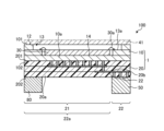
- the optical axis of the imaging device may shift due to thermal deformation of the substrate, and there is room for improvement in durability.
- FIG. 1 is a perspective view showing an example of an electrical device according to a first embodiment
- FIG. 2 is a cross-sectional view of the electrical device shown in FIG. 1;
- FIG. 1 is a perspective view showing an example of an electrical device according to a first embodiment
- FIG. 2 is a cross-sectional view of the electrical device shown in FIG. 1;
- FIG. 1 is a perspective view showing an example of an electrical device according to a first embodiment
- the electrical device 100 includes an electrical device mounting substrate 1 and an imaging device 30.
- the electric element mounting board 1 has a first board 10 and a second board 20 .
- the electric device mounting substrate 1 is a substrate or member for mounting the imaging device 30 .
- the first substrate 10 has ceramics as an insulating base material (first base material 10a).
- the first substrate 10 has a mounting area 11 and an installation portion 12 .
- the mounting area 11 is located in the central portion of the first surface 101 that is the upper surface of the first substrate 10 .
- the mounting area 11 is an area where the imaging element 30 is mounted.
- the mounting area 11 provided on the first substrate 10 may be referred to as a first mounting area.
- the surface on which the mounting area 11 and the installation portion 12 of the first substrate 10 are provided is referred to as a first surface 101 , and the surface opposite to the first surface 101 is referred to as a second surface 102 .
- the installation section 12 is positioned around the mounting area 11 .
- the installation portion 12 is positioned on the first surface 101 which is the top surface of the first substrate 10 . That is, in the case of the electric element mounting substrate 1 according to the first embodiment, the mounting area 11 and the installation portion 12 are positioned on the same plane of the first surface 101 . The mounting area 11 and the installation portion 12 are positioned at the same height on the first surface 101 . Since the electrical element mounting substrate 1 has a flat plate shape, a lens holder 40 may be installed on the installation portion 12 as shown in FIG. The lens holder 40 has an opening 40a. A lens 40 b is installed in the lens holder 40 .
- the second substrate 20 has an organic resin as an insulating base material (second base material 20a).
- the second substrate 20 is laminated on the first substrate 10 .
- the second substrate 20 is laminated on the second surface 102 located opposite to the first surface 101 of the first substrate 10 where the first mounting area is located.
- the surface of the second substrate 20 facing the first substrate 10 is referred to as a third surface, and the surface opposite to the third surface is referred to as a fourth surface.
- the installation portion 12 for installing the lens holder 40 is positioned around the mounting area 11 of the first substrate 10 made of ceramics as a base material in a plan view. located in Therefore, compared with the case where the lens holder 40 or the window material is placed on the organic base material, for example, positional displacement of the lens and optical axis displacement due to thermal deformation can be reduced. Thereby, the durability of the electric element mounting substrate 1 and the electric device 100 can be enhanced.
- the imaging element 30 is mounted on the mounting area 11 (first mounting area) of the electric element mounting board 1 .
- the imaging element 30 may be, for example, a CMOS (Complementary Metal Oxide Semiconductor), a CCD (Charge Coupled Device), or the like.
- the first base material 10a is, for example, a ceramic base material made of ceramics.
- the first base material 10a may be, for example, alumina-based or glass-ceramic ceramics, dielectric materials such as cordierite, zirconia, barium titanate, strontium titanate, calcium titanate, aluminum titanate, and zirconium titanate. Lead oxide (PZT) or the like may also be used.
- the first base material 10a may have, for example, a plurality of ceramics.
- a conductor layer may be formed on the surface of the first base material 10a, if necessary.
- a conductor layer may be, for example, a wire having a line shape, a pad having a circular shape, a rectangular shape or other angular shape, or a solid power supply layer or ground layer.
- the conductor located on the surface of the first base material 10a may be smaller than the area of the main surface of the first substrate 10, for example.
- the first substrate 10 may have a conductor layer (internal conductor layer) inside. Moreover, it may further have an interlayer connection conductor that electrically connects the surface conductor layer and the internal conductor layer.
- Materials for the surface conductor layer, the internal conductor layer and the interlayer connection conductor include, for example, tungsten (W), molybdenum (Mo), W--Mo mixtures, W--Mo alloys, W--Mo intermetallic compounds, and copper. , silver, nickel, and the like.
- the surface conductor layers, the internal conductor layers and the interlayer connection conductors may contain a common material such as ceramic powder.
- the interlayer connection conductor may contain, for example, copper powder, tin (Sn) powder, or bismuth (Bi) powder. Further, the interlayer connection conductor may have the same material as the second base material 20a, which will be described later, such as epoxy resin, as the remainder.
- the interlayer connection conductor preferably has a melting point closer to the heat-resistant temperature of the second substrate 20 made of organic resin than the heat-resistant temperature of the first substrate 10a made of ceramics.
- the second base material 20a is, for example, a so-called organic base material having an organic material.
- the second base material 20a may be epoxy resin, acrylic resin, polycarbonate resin, polyimide resin, olefin resin, or polyphenylene resin, for example.
- the second base material 20a may be, for example, polytetrafluoroethylene (PTFE) or other fluororesin or polyphenylene ether resin.
- PTFE polytetrafluoroethylene
- the second substrate 20 forming part of the electric element mounting substrate 1 is made of organic resin. For this reason, the weight of the electric element mounting substrate 1 and the electric device 100 can be reduced as compared with the case of having only a substrate made of ceramics as a base material.
- FIG. 3 is a perspective view showing an example of an electrical device according to the second embodiment.
- 4 is a cross-sectional view of the electrical device shown in FIG. 3.
- FIG. 3 is a perspective view showing an example of an electrical device according to the second embodiment. 4 is a cross-sectional view of the electrical device shown in FIG. 3.
- an electrical device 100 includes an electrical device mounting substrate 1 and an imaging device 30.
- the electric element mounting board 1 has a first board 10 and a second board 20 .
- the electric element mounting substrate 1 serves as a substrate or member for mounting the imaging element 30 .
- the first substrate 10 constituting the electric element mounting substrate 1 has the concave portion 13 .
- the recess 13 is located in the central portion of the first substrate 10 so as to have an opening on the first surface 101 of the first substrate 10 .
- the surface corresponding to the bottom of the recess 13 is the bottom surface 14 .
- the bottom surface 14 is a portion corresponding to the mounting area 11 (first mounting area) in the electric element mounting substrate 1 according to the second embodiment.
- the imaging device 30 is mounted on the bottom surface 14 of the recess 13, as shown in FIGS.
- the installation portion 12 for installing the lens holder 40 or the window member 41 is arranged around the bottom surface 14 on which the imaging device 30 is mounted in plan view.
- the installation portion 12 is provided on the first surface 101 of the electric element mounting substrate 1 .
- the installation portion 12 and the bottom surface 14 on which the imaging device 30 is mounted are different in height direction position when the electrical device mounting substrate 1 is viewed in a longitudinal section.
- the imaging device 30 can be arranged inside the concave portion 13 .
- the upper surface of the imaging device 30 can be arranged at a position lower than the position in the height direction of the first surface 101 of the electric device mounting substrate 1 .
- a flat window member 41 can be used for the installation portion 12 .
- the structure is such that the imaging element 30 does not protrude from the first surface 101 of the electric element mounting board 1 . As a result, the imaging device 30 is less susceptible to external and mechanical damage, and high reliability can be obtained.
- the window material 41 may be a translucent member such as glass.
- a window 41 a which is an area that can be imaged by the imaging device 30 , is positioned inside the installation portion 12 .
- a lens holder 40 may be installed instead of the window material 41 .
- the installation portion 12 for installing the window material 41 or the lens holder 40 can be positioned around the bottom surface 14 on which the imaging element 30 is mounted in plan view. can be done. For this reason, compared with the case where the window material 41 or the lens holder 40 is installed on the organic base material, for example, positional deviation of the window material 41 and the lens 40b due to thermal deformation of the electric element mounting board 1, and optical axis deviation can be reduced. Thereby, the durability of the electric element mounting substrate 1 and the electric device 100 can be enhanced.
- the window material 41 can be, for example, a flat plate shape whose entire surface is transparent. Therefore, light transmittance is increased, and more image information can be captured.
- first substrate 10 shown in FIG. 4 has a laminated structure, it may be a single-layer first substrate 10 provided with the concave portion 13 .
- the electric device 100 has a step 13a between the first surface 101 in the depth direction of the recess 13 and the bottom surface 14 .
- a terminal electrode 13b is provided on the step 13a, it becomes possible to connect a wire 30a for bonding extending from the imaging device 30 to this terminal electrode 13b.
- the height from the bottom surface 14 of the upper surface 30b of the imaging device 30 and the step 13a be the same or close to it. If the upper surface 30b of the imaging device 30 and the step 13a are at similar height positions, the length of the wire 30a from the imaging device 30 can be shortened. This makes it possible to reduce the increase in inductance due to the length of the wire 30a.
- the Young's modulus of the first substrate 10 may be higher than the Young's modulus of the second substrate 20 . Furthermore, the Young's modulus of the first substrate 10 may be higher than the Young's modulus of the window material 41 . Also, the Young's modulus of the first substrate 10 may be higher than the Young's modulus of the material of the lens holder 40 . In other words, the Young's modulus of the window material 41 and the Young's modulus of the lens holder 40 may be smaller than the Young's modulus of the first substrate 10 . The Young's modulus of the second substrate 20 may be smaller than the Young's modulus of the first substrate 10 .
- the electrical device 100 has a window material 41, a first substrate 10 and a second substrate 20 laminated in this order.
- the first substrate 10 having a high Young's modulus when the first substrate 10 having a high Young's modulus is arranged at the central position in the laminating direction, the first substrate 10 positioned at the central position in the laminating direction serves as a pivot, and the entire electric device 100 is constructed. deformation can be reduced.
- the Young's modulus may be measured using a sample piece cut out from the electrical device 100, or may be measured by separately fabricating a member corresponding to the composition of each base material.
- the main component is the component that is contained most in the base material in terms of mass ratio or volume ratio.
- FIG. 5 is a cross-sectional view showing an example of an electrical device according to the third embodiment.
- the electric element mounting board 1 has the same configuration as the electric element mounting board 1 of the first embodiment and the electric element mounting board 1 of the second embodiment. becomes. That is, in the case of the electric device 100 according to the third embodiment as well, the electric element mounting board 1 is a laminate of the first board 10 and the second board 20 . Also, the mounting structure of the imaging element 30 on the electric element mounting board 1 is the same as that of the electric device 100 of the second embodiment described above.
- the second substrate 20 has conductors 20b.
- the conductors 20 b may be provided on the surface (surfaces 201 and 202 ) and the interior 203 of the second substrate 20 . As shown in FIG. 5, the conductor 20b may be arranged so as to connect from a surface 201, which is one surface of the second substrate 20, to a surface 202, which is the other surface.
- the conductors 20b located on the second substrate 20 may have a smaller width or diameter than the conductors located on the first substrate 10.
- the conductor 20b has internal conductor layers 20b1 and 20b2 and interlayer connection conductors 20b3 and 20b4
- the width of the internal conductor layers 20b1 and 20b2 and/or the diameter of the interlayer connection conductors 20b3 and 20b4 are located on the first substrate 10. It may be smaller than the width of the surface conductor layer and/or the diameter of the interlayer connection conductor. As a result, for example, heat is less likely to be transmitted from the second substrate 20 side to the first substrate 10 side via the conductor.
- FIG. 6 is a cross-sectional view showing an example of an electrical device according to the fourth embodiment.
- the second substrate 20 has a heat dissipation portion 22 .
- the heat radiating portion 22 is a portion of the second substrate 20 that is close to the surface 202 .
- the heat radiation part 22 may have a higher volume ratio of the conductors 20 b than the other regions 22 a in the surface 202 of the second substrate 20 .
- the heat dissipation portion 22 of the second substrate 20 has a higher heat dissipation capability than the other regions 22a.
- the heat dissipation portion 22 may be arranged so as to surround the peripheral portion of the surface 202 of the second substrate 20 . Thereby, the heat dissipation from the second substrate 20 can be further improved.
- the central area 21 of the second substrate 20 excluding the heat radiating portion 22 may be used as a mounting portion of the second substrate 20 for the electric element.
- the heat radiation part 22 has a conductor 20b extending from the surface 201 of the second substrate 20 in contact with the first substrate 10 to the surface 202 of the second substrate 20 opposite to the surface 201, and the thickness of the second substrate 20. It may be arranged to extend outwardly of direction and surface 202 .
- the central region 21 is located in the central portion of the surface 202, which is the main surface of the second substrate 20, and is the region where the electrical elements are mounted.
- the heat radiating portion 22 is located around the region 21 and is a portion that radiates heat.
- the conductor 20 b located on the second substrate 20 may be exposed on the surface 202 of the heat radiating portion 22 .
- the heat transferred from the imaging element 30 through the first substrate 10 is radiated from the surface of the heat radiating section 22 to the surface 202 where the conductor 20b is exposed.
- heat can be dissipated from the first substrate 10 side to the second substrate 20 side. Even when an electric element is mounted in the central area 21, heat tends to flow toward the heat radiating part 22 around the central area 21, so that it is possible to suppress the occurrence of problems due to the inflow of heat to the electric element.
- the electrical device 100 may have the heat collecting member 50 on the surface 202 serving as the heat radiating portion 22 .
- the heat collecting member 50 is located, for example, at the heat radiation portion 22 of the second substrate 20 located around the central area 21 (second mounting area).
- the heat collecting member 50 is positioned so as to be in contact with the surface 202 of the second substrate 20 .
- the heat collecting member 50 is, for example, a member made of metal. According to the heat collecting member 50, the heat conducted through the conductor 20b can be collected and released to the outside air. In this way, by having the heat collecting member 50, for example, the influence of heat on other electric elements can be further reduced from the first substrate 10 side to the second substrate 20 side. heat can be dissipated.
- the heat radiating portion 22 or the heat collecting member 50 may be positioned so as to surround the area 21 .
- a structure in which the heat radiating portion 22 or the heat collecting member 50 serves as a wall member surrounding the region 21 from all sides may be employed. If the heat radiating part 22 or the heat collecting member 50 has a structure that serves as a wall member that surrounds the area 21 from all sides, for example, it has a function of protecting the electric elements 60 mounted in the area 21 described later from mechanical impacts. be able to. In this case, the height of the heat radiating portion 22 or the heat collecting member 50 should be higher than the height of the electric element 60 .
- the electrical device 100 may have a connector 80 for electrical connection with an external power supply.
- a part of the heat collecting member 50 may be used as the connector 80 .
- FIG. 7A is a cross-sectional view showing an example of an electrical device according to a fifth embodiment;
- the electrical device 100 according to the fifth embodiment has an electrical element 60 located on the surface 202 side of the second substrate 20 .
- the electrical element 60 is located in the region 21 and bonded to the surface 202 of the region 21 via the bonding material 65 .
- the electrical element 60 may be, for example, a semiconductor element for signal processing.
- the bonding material 65 may have conductivity, for example, and electrically connect the second substrate 20 and the electrical element 60 .
- the imaging element 30 is arranged on the bottom surface 14 of the concave portion 13 of the first substrate 10 .
- the electric element 60 is arranged on the surface 202 of the second substrate 20 laminated on the first substrate 10 .
- the imaging element 30 and the electric element 60 have overlapping portions in plan view. Even if the areas of the imaging element 30 and the electric element 60 are different, it is preferable that the entirety of either the imaging element 30 or the electric element 60 is placed within the plane of the other element.
- the shortest wiring length between the imaging element 30 and the electric element 60 can be set to a length corresponding to the thickness of the laminated first substrate 10 and the second substrate 20, so that the electric device 100 with small inductance can be obtained. can be done.
- the second base material 20a forming the second substrate 20 may have a lower dielectric constant than the first base material 10a forming the first substrate 10. As a result, signal delay can be reduced even when, for example, an electrical element with a higher operating frequency is arranged on the second substrate 20 side than on the first substrate 10 side.
- the electrical device 100 may have a heat dissipation member 70 .
- the heat dissipation member 70 is provided on the surface of the electric element 60 opposite to the surface on which the bonding material 65 is provided.
- the heat dissipation member 70 plays a role of quickly dissipating the heat generated in the electric element 60 . In this way, the heat generated by the electric element 60 is less likely to be transmitted to the imaging element 30 side through the electric element mounting substrate 1. Therefore, compared with the case where the heat dissipation member 70 is not provided, for example, the lens deformation due to thermal deformation is reduced. Positional deviation and optical axis deviation can be reduced. Thereby, the durability of the electric element mounting substrate 1 and the electric device 100 can be enhanced.
- the heat dissipation member 70 may be, for example, a heat dissipation plate. Also, the heat dissipation member 70 may have, for example, a heat sink or a fin member. In addition, when the heat sink is a pure solid, the heat sink may be used by overlapping the fin members.
- the second substrate 20 is provided with It is preferable to have a conductor 20 b and a portion of the conductor 20 b forms the heat radiating portion 22 on the peripheral edge of the surface 202 .
- the second board 20 may have a metal member inside.
- Such a metal member 20c may be a member that is arranged separately from the conductor 20b, is not energized, and only contributes to heat dissipation. That is, the metal member 20c located inside the second substrate 20 has a portion exposed to the side surface of the second substrate 20, but the metal member 20c is insulated from the conductor 20b that constitutes the electrical circuit. It should be in good condition. As a result, heat can be dissipated from the first substrate 10 side to the second substrate 20 side in such a manner that the influence of heat on other electronic elements can be reduced.
- the material of the conductor 20b and the metal member 20c of the second substrate 20 may be the same as the material of the conductor of the first substrate 10, for example. Also, conductor 20b and metal member 20c may have similar shapes and sizes.
- FIG. 7A may be a configuration in which the electric element 60, the second substrate 20, and the first substrate 10 are laminated in this order.
- FIG. 7B is a cross-sectional view showing another example of the electrical device according to the fifth embodiment.
- the electrical element 60 may be arranged in the mounting area of the second substrate 20 as shown in FIG. 7B. Also, the first substrate 10 may be arranged on the opposite side of the surface of the second substrate 20 on which the electric element 60 is arranged.
- the second substrate 20 may have a mounting area for mounting the electric element 60 on one main surface.
- the first substrate 10 may be arranged on the main surface of the second substrate 20 opposite to the surface on which the electric element 60 is mounted.
- the second substrate 20 may have a lower Young's modulus than the first substrate 10. If the second substrate 20 with the lower Young's modulus is the substrate on which the electrical element 60 is mounted, the stress on the electrical element 60 is reduced, and the probability of failure can be reduced. This can prevent the electric element mounting substrate 1 from being damaged together with the electric element 60 even when the electric element mounting substrate 1 is placed in a severe temperature environment such as an extremely low temperature.
- the arrangement of the conductors 20b may be upside down in the stacking direction compared to the case of FIG. 7A. That is, among the conductors 20b of the second substrate 20, the central conductors to which the internal conductor layers 20b1 and the interlayer connection conductors 20b3 are connected are the conductors on which the electrical device 60 is mounted when the electrical device mounting substrate 1 is viewed in the stacking direction. It may be located on the region side.
- the conductor to which the internal conductor layer 20b2 and the interlayer connection conductor 20b4 are connected is positioned closer to the surface opposite to the mounting area of the electric element 60 when the electric element mounting substrate 1 is viewed in the stacking direction. may be At this time, the conductors to which the internal conductor layers 20b2 and the interlayer connection conductors 20b4 are connected may be positioned around the mounting area when the electric element mounting substrate 1 is seen through from above.
- the conductor to which the internal conductor layer 20b2 and the interlayer connection conductor 20b4 are connected is arranged from the central conductor to which the internal conductor layer 20b1 and the interlayer connection conductor 20b3 are connected when the electric element mounting substrate 1 is viewed in longitudinal section. It may extend stepwise in the stacking direction of the electric element mounting substrate 1 .
- the central conductor to which the internal conductor layer 20b1 and the interlayer connection conductor 20b3 are connected and the conductor to which the internal conductor layer 20b2 and the interlayer connection conductor 20b4 are connected can enhance thermal conductivity between them. For this reason, it should be connected.
- the heat generated by the electric element 60 by the central conductor to which the internal conductor layer 20b1 and the interlayer connection conductor 20b3 are connected and the conductor to which the internal conductor layer 20b2 and the interlayer connection conductor 20b4 are connected is transferred to the electric element mounting substrate 1. Heat can be dissipated from the outside. Thereby, the driving stability of the electric element 60 can be achieved.
- the outside of the electric element mounting substrate 1 means that it includes the direction of the side surface of the substrate in addition to the thickness direction from the mounting area of the electric element mounting substrate 1 to the opposite side.
- the electric element 60 for example, a circuit element represented by a large scale integrated circuit (LSI), a switch ASIC element, a superconducting element (Josephson element), a SAW (surface acoustic wave) element, a light emitting element, a logic element, a hall At least one selected from the group consisting of an element, a light-receiving element, a piezoelectric element, a Peltier element, and a metal film resistance element may be used. Even in these cases, the electric element mounting board 1 having high durability can be obtained.
- the first substrate 10 and the second substrate 20 may have the same area in plan view.
- the second substrate 20 can be positioned so as to overlap the entire surface of the second surface 102 opposite to the first surface 101 where the first mounting area of the first substrate 10 is located. This makes it difficult for both the first substrate 10 and the second substrate 20 to warp locally when the substrates are laminated. Therefore, the durability of the electric element mounting substrate 1 and the electric device 100 can be enhanced.
- the first substrate 10 and the second substrate 20 may overlap with the same shape and size when seen from above.
- the effect of making local deformation of the first substrate 10 and the second substrate 20 less likely to occur can be enhanced.
- the first substrate 10 and the second substrate 20 overlap, if the area of the first substrate 10 is larger than the area of the second substrate 20, the portion of the first substrate 10 protruding from the second substrate 20 Deformation due to is likely to occur.
- the area of the second substrate 20 is larger than the area of the first substrate 10 , deformation due to the portion of the second substrate 20 protruding from the first substrate 10 is likely to occur.
- the side surface of the first substrate 10 and the side surface of the second substrate 20 overlap so as to be flush with each other.
- the first substrate 10 and the second substrate 20 are arranged such that the four side surfaces of the second substrate 20 arranged in the stacking direction are respectively opposite to the four side surfaces of the first substrate 10 . It is good to be on the same plane.
- the first substrate 10 and the second substrate 20 may be bonded together by the resin component contained in the second substrate 20. This makes it difficult for components other than the components contained in the first substrate 10 and the second substrate 20 to exist at the lamination interface between the first substrate 10 and the second substrate 20 . 20 can be enhanced.
- Ceramic green sheet examples include alumina-based ceramic materials and glass ceramics.
- a ceramic material containing alumina as a main component for example, one obtained by adding 10 to 20 parts by mass of SiO 2 and MgO to 100 parts by mass of raw alumina powder can be used. Also, an additive such as MnO may be further added. About the same amount of SiO 2 and MgO is preferable. The mass ratio of MnO is preferably 1/10 to 1/2 of the total amount of SiO 2 and MgO.
- glass ceramics for example, borosilicate glass containing inorganic particles such as alumina or silica can be used.
- the conductor pattern differs in the type of metal powder used as the main component between the ceramic material containing alumina as the main component and the glass ceramics.
- a conductor paste containing tungsten (W) and molybdenum (Mo) is used as a conductor pattern material because co-firing is possible.
- the ceramic green sheet formed of glass ceramics it is preferable to use a metal material, such as copper or silver, which is sintered at a lower temperature than tungsten or molybdenum, as the conductor pattern.
- a metal material such as copper or silver, which is sintered at a lower temperature than tungsten or molybdenum, as the conductor pattern.
- the pattern sheet may be formed by combining, for example, a conductor paste whose main component is copper or silver with high conductivity and glass ceramics.
- a ceramic material containing alumina as a main component may be sintered at, for example, 1500° C. to 1800° C., and a ceramic material containing glass ceramic as a main component may be fired at, for example, 800° C. to 1100° C.
- a plated film of Ni, Au, or the like may be formed as necessary.
- the first substrate 10 is formed.
- an inorganic or organic adhesive may be placed on the portion where the window member 41 (see FIGS. 3 and 4) is attached.
- the diameter (via diameter) of the interlayer connection conductor that penetrates each insulating layer can be set to 200 ⁇ m, for example.
- a copper foil having a thickness of 18 ⁇ m can be used as the metal member of the second substrate 20, for example.
- a varnish is prepared by adding an inorganic filler such as silica to an epoxy resin, and a green sheet is produced.
- the via conductors located in the thickness direction of the green sheet can be formed by, for example, forming a hole penetrating the green sheet in the thickness direction and then filling the inside of the formed through hole with a conductor paste.
- the conductor paste in this case is preferably a composite metal powder obtained by adding and mixing a low-melting-point metal to, for example, copper or silver powder.
- Tin (Sn), solder (Sn--Pb), bismuth (Bi), and antimony (Sb) can be exemplified as low resistance metal materials.
- the conductor paste may contain, as a binder, one or more organic resins selected from the group of epoxy resins, acrylic resins, polyethylene resins, and the like.
- the binder is preferably 1 to 20 parts by mass with respect to 100 parts by mass of the metal component.
- a copper foil pattern formed by etching a copper foil may be used for the ground layer and wiring.
- the copper foil pattern may be processed into a pattern shape by subjecting the copper foil to the resin film and then subjecting it to exposure and development.
- a copper foil pattern obtained by patterning is transferred to a green sheet. For the transfer, for example, after the copper foil pattern is attached to the green sheet, the resin film serving as the base material can be peeled off.
- a green sheet (patterned sheet) on which via conductors and copper foil patterns are formed is produced.
- a pattern sheet is laminated as it is on the back side of the first substrate 10 (for example, the second surface 102 shown in FIG. 4).
- the temperature is 70.degree.
- the produced laminate is cured at 200° C. to 250° C. for 2 to 4 hours. If necessary, plating (Ni, Au, etc.) may be formed on the surface of the conductor.
- solder resist may be formed in areas other than the copper foil pattern.
- the second substrate 20 As described above, the second substrate 20 according to each embodiment is formed, and the electric element mounting substrate 1 in which the first substrate 10 and the second substrate 20 are laminated is manufactured.
- FIG. 8 is an explanatory diagram showing a method of evaluating an electric element mounting board. First, the electric element mounting board 1 (10 mm square) shown in FIGS. Epoxy resin was used as the adhesive.
- the ring 91 was formed in the central portion of the window member 41 using Ag paste so that the outer diameter (diameter) was 5 mm and the inner diameter was 3 mm.
- a sample 2 was prepared in the same manner as the sample 1, except that the electric element mounting substrate disclosed in Patent Document 1 was used. Specifically, a first substrate having a recess on the top surface and containing an organic material, and a second substrate located in the recess of the first substrate and containing an inorganic material and having a mounting region on the top surface for mounting an imaging device. A substrate for mounting an electric element was prepared, and a window member 41 was attached thereto.
- the expansion coefficient of the ring 91 was 0.7%.
- the expansion coefficients of the ring 91 were 4% and 6%, respectively.
- the window material 41 is fixed to the first substrate 10 having an insulating base material made of ceramic. Therefore, it is considered that the window member 41 was difficult to deform.
- the electric element mounting substrate 1 includes the first substrate 10 having the first substrate 10a made of ceramics and the second substrate 20 having the second substrate 20a made of organic resin.
- the first substrate 10 has a first mounting area (for example, the mounting area 11) for mounting an electric element (for example, the imaging element 30), and an installation portion 12 for installing the lens holder 40 or the window material 41.
- the first mounting area is located on the top surface of the first substrate 10 .
- the installation portion 12 is positioned around the first mounting area in plan view.
- the second substrate 20 is laminated on the surface of the first substrate 10 opposite to the first mounting area.
Landscapes
- Engineering & Computer Science (AREA)
- Microelectronics & Electronic Packaging (AREA)
- Chemical & Material Sciences (AREA)
- Ceramic Engineering (AREA)
- Inorganic Chemistry (AREA)
- Manufacturing & Machinery (AREA)
- Solid State Image Pick-Up Elements (AREA)
- Cooling Or The Like Of Semiconductors Or Solid State Devices (AREA)
Priority Applications (4)
| Application Number | Priority Date | Filing Date | Title |
|---|---|---|---|
| EP22849626.1A EP4379803A1 (en) | 2021-07-30 | 2022-07-29 | Electrical element-mounting substrate and electrical device |
| JP2023538642A JP7813797B2 (ja) | 2021-07-30 | 2022-07-29 | 電気素子実装用基板および電気装置 |
| CN202280051249.8A CN117730415A (zh) | 2021-07-30 | 2022-07-29 | 电子元件安装用基板以及电子装置 |
| US18/293,247 US20240251505A1 (en) | 2021-07-30 | 2022-07-29 | Electrical element- mounting substrate and electrical device |
Applications Claiming Priority (2)
| Application Number | Priority Date | Filing Date | Title |
|---|---|---|---|
| JP2021-126316 | 2021-07-30 | ||
| JP2021126316 | 2021-07-30 |
Publications (1)
| Publication Number | Publication Date |
|---|---|
| WO2023008566A1 true WO2023008566A1 (ja) | 2023-02-02 |
Family
ID=85086892
Family Applications (1)
| Application Number | Title | Priority Date | Filing Date |
|---|---|---|---|
| PCT/JP2022/029326 Ceased WO2023008566A1 (ja) | 2021-07-30 | 2022-07-29 | 電気素子実装用基板および電気装置 |
Country Status (5)
| Country | Link |
|---|---|
| US (1) | US20240251505A1 (https=) |
| EP (1) | EP4379803A1 (https=) |
| JP (1) | JP7813797B2 (https=) |
| CN (1) | CN117730415A (https=) |
| WO (1) | WO2023008566A1 (https=) |
Cited By (2)
| Publication number | Priority date | Publication date | Assignee | Title |
|---|---|---|---|---|
| WO2025143247A1 (ja) * | 2023-12-28 | 2025-07-03 | 京セラ株式会社 | 配線基板および半導体デバイス |
| WO2025143246A1 (ja) * | 2023-12-28 | 2025-07-03 | 京セラ株式会社 | 配線基板および半導体デバイス |
Citations (8)
| Publication number | Priority date | Publication date | Assignee | Title |
|---|---|---|---|---|
| JP2011134777A (ja) * | 2009-12-22 | 2011-07-07 | Panasonic Electric Works Co Ltd | 回路基板、回路モジュール、回路基板の製造方法および回路モジュールの製造方法 |
| WO2014002860A1 (ja) * | 2012-06-29 | 2014-01-03 | ソニー株式会社 | カメラモジュールおよび電子機器 |
| JP2017037929A (ja) * | 2015-08-07 | 2017-02-16 | 日本特殊陶業株式会社 | 多層配線基板およびその製造方法 |
| JP2019009381A (ja) * | 2017-06-28 | 2019-01-17 | 京セラ株式会社 | 撮像装置用蓋体および撮像装置 |
| WO2019021705A1 (ja) * | 2017-07-25 | 2019-01-31 | ソニーセミコンダクタソリューションズ株式会社 | 固体撮像装置 |
| WO2019082923A1 (ja) | 2017-10-26 | 2019-05-02 | 京セラ株式会社 | 撮像素子実装用基板、撮像装置および撮像モジュール |
| WO2019087764A1 (ja) * | 2017-10-30 | 2019-05-09 | ソニーセミコンダクタソリューションズ株式会社 | 裏面照射型の固体撮像装置、および裏面照射型の固体撮像装置の製造方法、撮像装置、並びに電子機器 |
| JP2020004901A (ja) * | 2018-06-29 | 2020-01-09 | ソニーセミコンダクタソリューションズ株式会社 | 撮像装置および撮像装置の製造方法 |
-
2022
- 2022-07-29 JP JP2023538642A patent/JP7813797B2/ja active Active
- 2022-07-29 US US18/293,247 patent/US20240251505A1/en active Pending
- 2022-07-29 WO PCT/JP2022/029326 patent/WO2023008566A1/ja not_active Ceased
- 2022-07-29 EP EP22849626.1A patent/EP4379803A1/en not_active Withdrawn
- 2022-07-29 CN CN202280051249.8A patent/CN117730415A/zh active Pending
Patent Citations (8)
| Publication number | Priority date | Publication date | Assignee | Title |
|---|---|---|---|---|
| JP2011134777A (ja) * | 2009-12-22 | 2011-07-07 | Panasonic Electric Works Co Ltd | 回路基板、回路モジュール、回路基板の製造方法および回路モジュールの製造方法 |
| WO2014002860A1 (ja) * | 2012-06-29 | 2014-01-03 | ソニー株式会社 | カメラモジュールおよび電子機器 |
| JP2017037929A (ja) * | 2015-08-07 | 2017-02-16 | 日本特殊陶業株式会社 | 多層配線基板およびその製造方法 |
| JP2019009381A (ja) * | 2017-06-28 | 2019-01-17 | 京セラ株式会社 | 撮像装置用蓋体および撮像装置 |
| WO2019021705A1 (ja) * | 2017-07-25 | 2019-01-31 | ソニーセミコンダクタソリューションズ株式会社 | 固体撮像装置 |
| WO2019082923A1 (ja) | 2017-10-26 | 2019-05-02 | 京セラ株式会社 | 撮像素子実装用基板、撮像装置および撮像モジュール |
| WO2019087764A1 (ja) * | 2017-10-30 | 2019-05-09 | ソニーセミコンダクタソリューションズ株式会社 | 裏面照射型の固体撮像装置、および裏面照射型の固体撮像装置の製造方法、撮像装置、並びに電子機器 |
| JP2020004901A (ja) * | 2018-06-29 | 2020-01-09 | ソニーセミコンダクタソリューションズ株式会社 | 撮像装置および撮像装置の製造方法 |
Cited By (2)
| Publication number | Priority date | Publication date | Assignee | Title |
|---|---|---|---|---|
| WO2025143247A1 (ja) * | 2023-12-28 | 2025-07-03 | 京セラ株式会社 | 配線基板および半導体デバイス |
| WO2025143246A1 (ja) * | 2023-12-28 | 2025-07-03 | 京セラ株式会社 | 配線基板および半導体デバイス |
Also Published As
| Publication number | Publication date |
|---|---|
| EP4379803A1 (en) | 2024-06-05 |
| JP7813797B2 (ja) | 2026-02-13 |
| CN117730415A (zh) | 2024-03-19 |
| JPWO2023008566A1 (https=) | 2023-02-02 |
| US20240251505A1 (en) | 2024-07-25 |
Similar Documents
| Publication | Publication Date | Title |
|---|---|---|
| JP4329884B2 (ja) | 部品内蔵モジュール | |
| CN206976318U (zh) | 模块 | |
| US6979890B2 (en) | Intermediate substrate | |
| US7768122B2 (en) | Semiconductor package | |
| US20250221079A1 (en) | Wiring board and semiconductor device | |
| JP6788044B2 (ja) | 熱電素子内蔵パッケージ | |
| JP4915058B2 (ja) | Led部品およびその製造方法 | |
| WO2004055891A9 (ja) | 半導体装置および積層型半導体装置 | |
| KR20170125095A (ko) | 광소자 탑재용 패키지, 전자 장치 및 전자 모듈 | |
| JP7813797B2 (ja) | 電気素子実装用基板および電気装置 | |
| JP6791719B2 (ja) | 電子部品搭載用基板、電子装置および電子モジュール | |
| JP5942594B2 (ja) | 半導体装置 | |
| JP2014157949A (ja) | 配線基板および電子装置 | |
| JP6329065B2 (ja) | 電子素子実装用基板および電子装置 | |
| JP7088749B2 (ja) | 電子素子実装用基板、電子装置、および電子モジュール | |
| US10236228B2 (en) | Electronic component mounting board, electronic device, and electronic module | |
| JP7299121B2 (ja) | 回路基板、電子部品および電子モジュール | |
| JP2011114019A (ja) | 回路モジュールおよび回路モジュールの実装方法 | |
| US10388628B2 (en) | Electronic component package | |
| JP4057843B2 (ja) | 多層回路基板 | |
| JP7212783B2 (ja) | 電子素子実装用基板、電子装置、電子モジュールおよび電子素子実装用基板の製造方法 | |
| US20240355845A1 (en) | Electronic element mounting substrate, electronic device, and electronic module | |
| JP7209749B2 (ja) | 電子部品実装用基体および電子装置 | |
| WO2025143199A1 (ja) | 配線基板および半導体デバイス | |
| WO2025143198A1 (ja) | 配線基板および半導体デバイス |
Legal Events
| Date | Code | Title | Description |
|---|---|---|---|
| 121 | Ep: the epo has been informed by wipo that ep was designated in this application |
Ref document number: 22849626 Country of ref document: EP Kind code of ref document: A1 |
|
| WWE | Wipo information: entry into national phase |
Ref document number: 2023538642 Country of ref document: JP |
|
| WWE | Wipo information: entry into national phase |
Ref document number: 202280051249.8 Country of ref document: CN |
|
| WWE | Wipo information: entry into national phase |
Ref document number: 18293247 Country of ref document: US |
|
| WWE | Wipo information: entry into national phase |
Ref document number: 2022849626 Country of ref document: EP |
|
| NENP | Non-entry into the national phase |
Ref country code: DE |
|
| ENP | Entry into the national phase |
Ref document number: 2022849626 Country of ref document: EP Effective date: 20240229 |
|
| WWW | Wipo information: withdrawn in national office |
Ref document number: 2022849626 Country of ref document: EP |