WO2023008059A1 - コネクタシステム - Google Patents
コネクタシステム Download PDFInfo
- Publication number
- WO2023008059A1 WO2023008059A1 PCT/JP2022/025901 JP2022025901W WO2023008059A1 WO 2023008059 A1 WO2023008059 A1 WO 2023008059A1 JP 2022025901 W JP2022025901 W JP 2022025901W WO 2023008059 A1 WO2023008059 A1 WO 2023008059A1
- Authority
- WO
- WIPO (PCT)
- Prior art keywords
- board
- wire
- outer conductor
- connector
- side connector
- Prior art date
Links
- 239000004020 conductor Substances 0.000 claims abstract description 196
- 229910052751 metal Inorganic materials 0.000 claims description 35
- 239000002184 metal Substances 0.000 claims description 35
- 229920003002 synthetic resin Polymers 0.000 claims description 15
- 239000000057 synthetic resin Substances 0.000 claims description 15
- 239000000463 material Substances 0.000 claims description 14
- 230000013011 mating Effects 0.000 claims description 12
- 238000005266 casting Methods 0.000 claims description 10
- 239000000758 substrate Substances 0.000 abstract description 19
- 238000004519 manufacturing process Methods 0.000 description 11
- 238000005452 bending Methods 0.000 description 6
- 210000000078 claw Anatomy 0.000 description 6
- 238000000034 method Methods 0.000 description 5
- 238000004512 die casting Methods 0.000 description 3
- 230000000149 penetrating effect Effects 0.000 description 3
- 238000003825 pressing Methods 0.000 description 3
- 238000005520 cutting process Methods 0.000 description 2
- 230000000694 effects Effects 0.000 description 2
- 238000001746 injection moulding Methods 0.000 description 2
- 238000005476 soldering Methods 0.000 description 2
- 229910000838 Al alloy Inorganic materials 0.000 description 1
- RYGMFSIKBFXOCR-UHFFFAOYSA-N Copper Chemical compound [Cu] RYGMFSIKBFXOCR-UHFFFAOYSA-N 0.000 description 1
- 229910000881 Cu alloy Inorganic materials 0.000 description 1
- HCHKCACWOHOZIP-UHFFFAOYSA-N Zinc Chemical compound [Zn] HCHKCACWOHOZIP-UHFFFAOYSA-N 0.000 description 1
- 230000004308 accommodation Effects 0.000 description 1
- 229910052782 aluminium Inorganic materials 0.000 description 1
- XAGFODPZIPBFFR-UHFFFAOYSA-N aluminium Chemical compound [Al] XAGFODPZIPBFFR-UHFFFAOYSA-N 0.000 description 1
- 238000004891 communication Methods 0.000 description 1
- 239000002131 composite material Substances 0.000 description 1
- 229910052802 copper Inorganic materials 0.000 description 1
- 239000010949 copper Substances 0.000 description 1
- 238000005516 engineering process Methods 0.000 description 1
- 238000012986 modification Methods 0.000 description 1
- 230000004048 modification Effects 0.000 description 1
- 229920005989 resin Polymers 0.000 description 1
- 239000011347 resin Substances 0.000 description 1
- 230000000717 retained effect Effects 0.000 description 1
- 229910052725 zinc Inorganic materials 0.000 description 1
- 239000011701 zinc Substances 0.000 description 1
Images


Classifications
-
- H—ELECTRICITY
- H01—ELECTRIC ELEMENTS
- H01R—ELECTRICALLY-CONDUCTIVE CONNECTIONS; STRUCTURAL ASSOCIATIONS OF A PLURALITY OF MUTUALLY-INSULATED ELECTRICAL CONNECTING ELEMENTS; COUPLING DEVICES; CURRENT COLLECTORS
- H01R12/00—Structural associations of a plurality of mutually-insulated electrical connecting elements, specially adapted for printed circuits, e.g. printed circuit boards [PCB], flat or ribbon cables, or like generally planar structures, e.g. terminal strips, terminal blocks; Coupling devices specially adapted for printed circuits, flat or ribbon cables, or like generally planar structures; Terminals specially adapted for contact with, or insertion into, printed circuits, flat or ribbon cables, or like generally planar structures
- H01R12/70—Coupling devices
- H01R12/71—Coupling devices for rigid printing circuits or like structures
-
- H—ELECTRICITY
- H01—ELECTRIC ELEMENTS
- H01R—ELECTRICALLY-CONDUCTIVE CONNECTIONS; STRUCTURAL ASSOCIATIONS OF A PLURALITY OF MUTUALLY-INSULATED ELECTRICAL CONNECTING ELEMENTS; COUPLING DEVICES; CURRENT COLLECTORS
- H01R13/00—Details of coupling devices of the kinds covered by groups H01R12/70 or H01R24/00 - H01R33/00
- H01R13/648—Protective earth or shield arrangements on coupling devices, e.g. anti-static shielding
- H01R13/658—High frequency shielding arrangements, e.g. against EMI [Electro-Magnetic Interference] or EMP [Electro-Magnetic Pulse]
- H01R13/6581—Shield structure
- H01R13/6582—Shield structure with resilient means for engaging mating connector
-
- H—ELECTRICITY
- H01—ELECTRIC ELEMENTS
- H01R—ELECTRICALLY-CONDUCTIVE CONNECTIONS; STRUCTURAL ASSOCIATIONS OF A PLURALITY OF MUTUALLY-INSULATED ELECTRICAL CONNECTING ELEMENTS; COUPLING DEVICES; CURRENT COLLECTORS
- H01R13/00—Details of coupling devices of the kinds covered by groups H01R12/70 or H01R24/00 - H01R33/00
- H01R13/648—Protective earth or shield arrangements on coupling devices, e.g. anti-static shielding
- H01R13/658—High frequency shielding arrangements, e.g. against EMI [Electro-Magnetic Interference] or EMP [Electro-Magnetic Pulse]
- H01R13/6591—Specific features or arrangements of connection of shield to conductive members
- H01R13/6594—Specific features or arrangements of connection of shield to conductive members the shield being mounted on a PCB and connected to conductive members
Definitions
- the present disclosure relates to connector systems.
- Patent Document 1 JP-A-2011-49118
- Patent Document 2 JP-A-2020-109738
- the board-side connector described in JP-A-2011-49118 has an outer conductor made of a metal plate. Manufacturing costs can be reduced by forming the outer conductor by bending a metal plate.
- the board-side connector described in JP-A-2020-109738 has an outer conductor formed by casting, die-casting, cutting, or the like.
- the outer conductor formed by the above method does not have a gap, unlike the outer conductor made of a metal plate. Therefore, it is less likely to be affected by noise, and can be suitably applied to high-speed communication.
- the manufacturing cost increases compared to the outer conductor made of a metal plate material.
- the shape of the outer conductor made of metal plate material differs from that of the outer conductor formed by casting or the like. Therefore, a board-side connector having an outer conductor made of a metal plate and a board-side connector having an outer conductor formed by casting or the like are designed separately.
- the wire connector that is mated with the board-side connector was also designed individually in correspondence with the board-side connector that was designed individually. Therefore, there is a problem that the manufacturing cost increases for both the board-side connector and the wire connector.
- the present disclosure has been completed based on the circumstances as described above, and aims to provide technology related to a connector system with reduced manufacturing costs.
- the present disclosure is a connector system including a wire-side connector connected to an end of an electric wire and a plurality of types of board-side connectors connected to a circuit board, wherein the wire-side connector is connected to the end of the electric wire.
- a wire-side inner conductor connected to a part, a metal wire-side outer conductor covering the wire-side inner conductor while being electrically insulated from the wire-side inner conductor, and a composite holding the wire-side outer conductor a resin wire-side connector housing
- each of the plurality of types of board-side connectors includes a board-side inner conductor connected to a conductive path provided on the circuit board; a board-side outer conductor made of metal covering the board-side inner conductor in a substantially insulated state; and a board-side connector housing made of synthetic resin for holding the board-side outer conductor, wherein the wire-side inner conductor and the board-side inner conductor are electrically connectable, the wire-side outer conductor and the board-side outer conductor are electrical
- the manufacturing cost of the connector can be reduced.
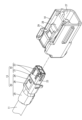
- FIG. 1 is a perspective view showing a wire-side connector according to Embodiment 1.
- FIG. FIG. 2 is an exploded perspective view showing the wire-side connector housing and the wire-side outer conductor connected to the end of the wire in the wire-side connector.
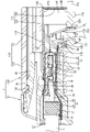
- FIG. 3 is a side cross-sectional view showing a state in which the wire-side connector and the first board-side connector are fitted together.
- FIG. 4 is a side sectional view showing a state in which the wire-side connector and the second board-side connector are fitted together.
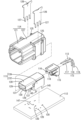
- FIG. 5 is a perspective view showing the first board-side connector attached to the first circuit board.
- FIG. 6 is an exploded perspective view showing the first board-side connector.
- FIG. 7 is a perspective view showing the second board side connector attached to the second circuit board.
- FIG. 8 is an exploded perspective view showing a second board side connector.
- the present disclosure is a connector system including a wire-side connector connected to an end of a wire and a plurality of types of board-side connectors connected to a circuit board, wherein the wire-side connector includes the A wire-side inner conductor connected to an end of a wire, a metal wire-side outer conductor covering the wire-side inner conductor while being electrically insulated from the wire-side inner conductor, and the wire-side outer conductor.
- a wire-side connector housing made of synthetic resin for holding each of the plurality of types of board-side connectors, each of which includes a board-side inner conductor connected to a conductive path provided on the circuit board; a substrate-side outer conductor made of metal that covers the substrate-side inner conductor in a state of being electrically insulated from the conductor; and a board-side connector housing made of synthetic resin that holds the board-side outer conductor;
- the side inner conductor and the board-side inner conductor are electrically connectable, the wire-side outer conductor and the board-side outer conductor are electrically connectable, and the wire-side connector housing and the board-side connector are connected.
- the plurality of types of board-side connectors each have a different board-side outer conductor, and one board-side connector selected from the plurality of types of board-side connectors is connected to the electric wire. It is designed to mate with the side connector.
- the wire-side connector can be shared for multiple types of board-side connectors, the wire-side connector can be individually designed for multiple types of board-side connectors. The manufacturing cost can be reduced as compared with the case where
- wire-side connector housing can also be shared, manufacturing costs can be further reduced.
- the plurality of types of board-side connectors include a first board-side connector having a first board-side outer conductor made of a bent metal plate, and a second board-side connector having a second board-side outer conductor formed by casting. , is preferably included.
- the manufacturing cost of the first board side connector can be reduced.
- the shield performance of the second board side connector can be improved.
- the first board-side outer conductor of the first board-side connector has a tubular shape and has a first fitting tubular portion into which the wire-side outer conductor is fitted, and the first fitting tubular portion has a mating end where the edges of the metal plate material constituting the first board-side outer conductor abut against each other, the wire-side outer conductor has an elastic contact portion that can be elastically deformed, and the elastic contact portion is It is preferable to elastically contact a portion of the first fitting cylinder portion that is different from the mating end portion.
- FIG. 1 Embodiment 1 of the present disclosure will be described with reference to FIGS. 1 to 8.
- FIG. The connector system 1 is mounted on a vehicle (not shown) such as an electric vehicle or a hybrid vehicle. etc.) or between in-vehicle electrical components.
- the connector system 1 includes a wire-side connector 10 , a first board-side connector 110 , and a second board-side connector 210 different from the first board-side connector 110 .
- the wire-side connector 10 is fitted with one selected from the first board-side connector 110 and the second board-side connector 210 .
- the direction in which the wire-side connector 10, the first board-side connector 110, and the second board-side connector 210 are fitted is defined as the front. Further, in some cases, with respect to a plurality of identical members, only some of the members are given reference numerals, and the reference numerals of other members are omitted.
- the wire-side connector 10 includes a wire-side inner conductor 12 connected to the end of the wire 11 and a wire-side inner conductor 12 electrically insulated from the wire-side inner conductor 12 . 12 and a wire-side connector housing 14 made of synthetic resin that holds the wire-side outer conductor 13 . As shown in FIG. 3, a wire-side dielectric 15 is arranged between the wire-side inner conductor 12 and the wire-side outer conductor 13 . The wire-side inner conductor 12 and the wire-side outer conductor 13 are electrically insulated by the wire-side dielectric 15 .
- the electric wire 11 includes two covered electric wires 16 to which the electric wire-side inner conductors 12 are connected, a shield portion 17 made of a braided wire that collectively covers the outer circumference of the covered electric wire 16, and a shield portion 17. and a sheath portion 18 made of an insulating synthetic resin that covers the outer periphery.
- the shield part 17 exposed from the stripped end of the sheath part 18 is folded back onto the end of the sheath part 18.
- the two coated wires 16 protruding forward from the folded sheath portion 18 are held by a clip 31 formed by bending a metal plate material.
- the wire-side inner conductor 12 is housed inside the wire-side dielectric 15 .
- the wire-side dielectric 15 is made of insulating synthetic resin.
- the wire-side dielectric 15 is formed in a rectangular parallelepiped shape elongated in the front-rear direction.
- the wire-side dielectric 15 has an upper dielectric 32 opening downward and a lower dielectric 33 assembled to the upper dielectric 32 from below. With the upper dielectric 32 and the lower dielectric 33 assembled, the two wire-side inner conductors 12 connected to the coated wire 16 are housed in the wire-side dielectric 15 side by side in the left-right direction.
- the wire-side outer conductor 13 is fitted with the first board-side outer conductor 111 of the first board-side connector 110 or the second board-side outer conductor 211 of the second board-side connector 210. It is possible to connect.
- the wire-side outer conductor 13 includes a lower outer conductor 19 that covers the outer periphery of the wire-side dielectric 15, and a shield portion 17 that is folded back on the lower outer conductor 19 and the sheath portion 18. and an upper outer conductor 20 assembled to the lower outer conductor 19 .
- the lower outer conductor 19 is formed by processing a conductive metal plate material by pressing or the like. As shown in FIG. 2, the lower outer conductor 19 has a tubular portion 21 that accommodates the wire-side dielectric 15 .
- the tubular portion 21 is formed in a square tubular shape that is substantially rectangular in front view, and the first substrate side outer conductor 111 or the second substrate side outer conductor 111 is provided outside the tubular portion 21 .
- a conductor 211 is made fittable.
- An elastic contact portion 23 that protrudes outward in the radial direction of the tubular portion 21 and is elastically deformable is formed at a position near the front end portion of the tubular portion 21 .
- Elastic contact portions 23 are provided on each of the upper surface, the lower surface, and the left and right side surfaces of the cylindrical portion 21 .
- the elastic contact portion 23 contacts the inner wall of the first board-side outer conductor 111 or the second board-side outer conductor 211 . is designed to come into contact with from the inside.
- the upper outer conductor 20 is formed by processing a conductive metal plate material by pressing or the like.
- the upper outer conductor 20 includes, as shown in FIG. 25.
- the cover part 24 is formed in a size that covers from above the area from the rear part of the cylindrical part 21 to the shield part 17 folded back onto the sheath part 18 .
- a square-shaped lance hole 26 is formed through the upper surface of the cover portion 24 in the vertical direction.
- connection barrel 25 is provided at the rear portion of the cover portion 24 .
- the connection barrel 25 is crimped so as to cover the outer circumference of the shield portion 17 folded back on the sheath portion 18 .
- the wire-side outer conductor 13 composed of the lower outer conductor 19 and the upper outer conductor 20 is electrically connected to the shield portion 17 of the wire 11 .
- the wire-side connector housing 14 is made of insulating synthetic resin and has a housing portion 27 penetrating in the front-rear direction.
- a lock arm 28 extending rearward from the front end of the wire-side connector housing 14 is formed on the upper surface of the wire-side connector housing 14 .
- the lock arm 28 is formed in a cantilever shape that can bend and deform in the vertical direction with the front end as a fulcrum.
- a lock projection 29 is formed on the upper surface of the lock arm 28 and protrudes upward.
- the accommodating portion 27 is formed in a substantially square tubular shape that penetrates the wire-side connector housing 14 in the front-rear direction.
- a lance 30 that can be engaged with the edge of the lance hole 26 provided in the wire-side outer conductor 13 is provided in the accommodating portion 27 (see FIGS. 3 and 4).
- the tip of the lance 30 is fitted into the lance hole 26 as shown in FIGS. are adapted to be engaged with the edge of the As a result, the wire-side outer conductor 13 is retained in the wire-side connector housing 14 so as to be prevented from coming off.
- the first board-side connector 110 is attached to the surface of the first circuit board 112, as shown in FIG. As shown in FIG. 6 , the first board-side connector 110 includes a first board-side inner conductor 113 made of a conductive metal and a first board-side inner conductor 113 that is electrically insulated from the first board-side inner conductor 113 .
- a first board-side outer conductor 111 made of a conductive metal covering 113 and a first board-side connector housing 114 made of insulating synthetic resin that holds the first board-side outer conductor 111 are provided.
- a first substrate side dielectric 115 made of insulating synthetic resin is arranged between the first substrate side inner conductor 113 and the first substrate side outer conductor 111 .
- the first substrate-side inner conductor 113 and the first substrate-side outer conductor 111 are electrically insulated by the first substrate-side dielectric 115 .
- the first substrate-side dielectric 115 is L-shaped when viewed from the side.
- the first substrate-side dielectric 115 has a plurality of mounting holes 116 penetrating in the front-rear direction.
- Each mounting hole 116 is provided side by side in a pair.
- the first substrate-side inner conductor 113 includes a straight portion 117 extending in the front-rear direction, a bent portion 118 extending downward from the rear end of the straight portion 117, and a connecting portion extending rearward from the lower end of the bent portion 118. and a portion 119 .
- the front portion of the straight portion 117 is electrically connected to the wire-side inner conductor 12 attached to the wire-side connector 10 when it is fitted with the wire-side connector 10 (see FIG. 3).
- the straight portion 117 of the first substrate-side inner conductor 113 is inserted into the mounting hole 116 of the first substrate-side dielectric 115 .
- the first-substrate-side inner conductor 113 is attached to the first-substrate-side dielectric 115 so as to prevent it from coming off.
- the front portion of the straight portion 117 protrudes forward from the first substrate-side dielectric 115, and the bent portion 118 and connecting portion 119 are arranged extending downward.
- the connecting portion 119 is inserted into a through hole 120 formed in the first circuit board 112 and soldered to a conductive path 147 formed in the first circuit board 112 .
- the conductive paths 147 of the first circuit board 112 and the first board-side inner conductors 113 are electrically connected.
- the first board-side connector housing 114 has a housing base portion 121 having an accommodating portion 124 and a hood portion 122 projecting forward from the housing base portion 121 .
- the hood portion 122 has a hook portion 123 which projects downward and engages with the lock projection 29 of the wire side connector 10 at the front end of the inner surface of the upper wall. .
- the housing portion 124 penetrates the housing base portion 121 in the front-rear direction and opens to the lower surface of the housing base portion 121 .
- the housing base portion 121 can accommodate the first substrate-side outer conductor 111 in the accommodation portion 124 .
- the first board-side connector housing 114 has fixture mounting grooves 125 on both side surfaces of the housing base 121 .
- a fixture 126 made of a metal plate is attached to each fixture mounting groove 125 from above.
- a plurality of (three in this embodiment) connection portions 127 extend downward from the lower end portion of the fixture 126 .
- the first board-side connector 110 is fixed to the first circuit board 112 by fixing the connecting portion 127 to the through hole 120 formed in the first circuit board 112 by soldering.
- the first substrate-side outer conductor 111 is formed by pressing and bending a sheet of metal plate material. As shown in FIG. 6 , the first substrate-side outer conductor 111 has a top plate portion 128 , two side plate portions 129 and a bottom plate portion 130 . The top plate portion 128 and the bottom plate portion 130 face each other in the vertical direction, and the side plate portions 129 face each other in the width direction (horizontal direction). As shown in FIG. 9, the bottom plate portion 130 has a mating end portion 131 in the center portion in the width direction. The first substrate-side outer conductor 111 is prevented from opening by dove-fitting the mating end portion 131 of the bottom plate portion 130 and meshing in an uneven shape, so that the box shape can be maintained.
- the first substrate-side outer conductor 111 has a tubular first fitting tubular portion 132 .
- the first fitting cylinder portion 132 has an inner side defined by the top plate portion 128, the side plate portions 129, and the bottom plate portion 130 penetrating in the front-rear direction.
- the first substrate-side dielectric 115 is held in the first fitting cylinder portion 132 in a state of being prevented from coming off while being inserted into the first fitting cylinder portion 132 .
- the first board-side outer conductor 111 has a projecting piece 136 shaped like a rectangular plate when viewed from the front and extending bent downward from the rear end of the bottom plate portion 130 of the first fitting cylinder portion 132 .
- the protruding piece 136 is provided at the central position of the bottom plate portion 130 in the left-right direction.
- a connecting portion 137 extending downward is formed at the lower end portion of the projecting piece 136 .
- the connection portion 137 is inserted into the through hole 120 formed in the first circuit board 112 and soldered to be electrically connected to the conductive path 147 of the first circuit board 112 .
- the protruding piece 136 and the connecting portion 137 are provided with the matching end portion 131 at the central position in the left-right direction.
- the first substrate-side outer conductor 111 has a lid member 139 integrally formed with the top plate portion 128 via a hinge portion 138 at the rear end portion of the top plate portion 128 .
- Lid member 139 is formed to be rotatable about hinge portion 138 .
- the cover member 139 includes a rectangular back portion 140 extending in the vertical direction and the width direction, and upper and lower portions protruding forward from both side ends of the back portion 140. It integrally has two side portions 141 along the direction and the front-rear direction, and a covering portion 142 constructed between the front ends of the two side portions 141 .
- the back portion 140 has a flat plate surface with no irregularities in the front and rear, and is sized to cover the entire opening on the rear side of the board-side outer conductor (see FIG. 3).
- Each side portion 141 can cover the rear portion of the outer surface (each side surface) of each side plate portion 129 of the first substrate-side outer conductor 111 .
- connection portions 145 are formed to extend downward and are spaced apart in the front-rear direction.
- the connecting portion 145 is inserted into the through hole 120 formed in the first circuit board 112 and soldered to be electrically connected to the conductive path 147 of the first circuit board 112 .
- hook-shaped holding parts 146 extending downward and bending upward are formed at intervals in the left-right direction.
- the holding portion 146 is curved in a substantially S shape when viewed from the side.
- the projecting piece 136 is sandwiched between the holding portion 146 and the cover portion 142 . This prevents the lid member 139 from rotating about the hinge portion 138 .
- the first substrate-side dielectric 115 is inserted into the first fitting cylindrical portion 132 of the first substrate-side outer conductor 111, and then Further, by bending the hinge portion 138, the cover member 139 is rotated around the hinge portion 138, and the cover member 139 closes the rear opening of the first fitting cylindrical portion 132. .
- the second board-side connector 210 is attached to the surface of the second circuit board 212, as shown in FIGS. As shown in FIG. 8, the second-board-side connector 210 includes a second-board-side inner conductor 213 made of a conductive metal and a second-board-side inner conductor 213 that is electrically insulated from the second-board-side inner conductor 213 .
- a second board-side outer conductor 211 made of a conductive metal covering 213 and a second board-side connector housing 214 made of insulating synthetic resin that holds the second board-side outer conductor 211 are provided.
- a second substrate side dielectric 215 made of insulating synthetic resin is arranged between the second substrate side inner conductor 213 and the second substrate side outer conductor 211 .
- the second substrate side inner conductor 213 and the second substrate side outer conductor 211 are electrically insulated by the second substrate side dielectric 215 .
- the second board-side connector housing 214 is formed by injection molding an insulating synthetic resin.
- the second board-side connector housing 214 opens forward (an example of an opening direction) and includes a receptacle 216 into which the wire-side connector 10 is fitted.
- a rear wall 217 is provided on the side opposite to the open end of the receptacle 216 in the second board side connector housing.
- a claw portion 218 that protrudes downward is formed on the front edge (open end portion) of the upper wall of the hood portion 216 .
- the claws 218 are engaged with the locking projections 29 of the wire-side connector 10 fitted inside the hood 216 so that the wire-side connector 10 is held inside the hood 216. It has become.
- locking projections 219 projecting rearward are formed at the four corners.
- the locking projection 219 is formed in a cylindrical shape.
- a mounting hole 220 through which the second substrate-side outer conductor 211 is inserted is formed in the back wall 217 so as to penetrate the back wall 217 in the front-rear direction.
- the cross-sectional shape of the mounting hole 220 is rectangular with rounded corners.
- the second substrate-side outer conductor 211 is made of metal having conductivity.
- any metal such as zinc, copper, copper alloy, aluminum, aluminum alloy, etc. can be appropriately selected.
- the second substrate-side outer conductor 211 is formed by known methods such as casting, die casting, and cutting. In this embodiment, the second substrate-side outer conductor 211 is formed by casting or die casting.
- the second board-side outer conductor 211 is in electrical contact with the wire-side outer conductor 13 accommodated in the wire-side connector 10 (see FIG. 4).
- the second-board-side outer conductor 211 includes a cylindrical portion 221 extending in the front-rear direction and having a cylindrical shape, a dielectric enclosing portion 222 extending rearward from the rear end edge of the cylindrical portion 221, and a cylindrical portion. and a flange 223 protruding in a direction intersecting the front-rear direction at a boundary portion between 221 and the dielectric enclosing portion 222 .
- the cross-sectional shape of the tubular portion 221 is rectangular with rounded corners.
- the outer shape of the tubular portion 221 is set to be the same as or slightly smaller than the inner shape of the attachment hole 220 of the back wall 217 . Thereby, the cylindrical portion 221 is press-fitted into the mounting hole 220 .
- the dielectric enclosure 222 is open downward and rearward. Inside the dielectric enclosing part 222 , the second substrate side dielectric 215 is accommodated while being surrounded by the dielectric enclosing part 222 on the upper side, the right side, and the left side.
- connection portion 224 protruding downward are provided at the lower end portion of the dielectric enclosing portion 222 .
- the connection portion 224 is penetrated through the through hole 225 of the second circuit board 212 and connected to the conductive path 231 formed on the inner surface of the through hole 225 by a known technique such as soldering.
- soldering a known technique such as soldering.
- the second-board-side outer conductor 211 is electrically connected to the conductive path 231 formed on the second circuit board 212 .
- the flange 223 contacts the rear surface of the back wall 217 from behind while the tubular portion 221 is press-fitted into the mounting hole 220 .
- locking recesses 226 are formed at positions corresponding to the locking projections 219 of the back wall 217 , respectively.
- the cross-sectional shape of the engaging recess 226 is circular.
- the inner shape of the locking recess 226 is set substantially the same as the outer shape of the locking projection 219 .
- the second substrate side dielectric 215 is made by injection molding a synthetic resin having insulating properties. As shown in FIG. 8, the second substrate side dielectric 215 is formed in an L shape when viewed from the side.
- the second substrate side dielectric 215 has an inner conductor accommodating chamber 227 capable of accommodating the second substrate side inner conductor 213 therein.
- the inner conductor accommodating chamber 227 is formed so as to pass through the second substrate side dielectric 215 in the front-rear direction and also open on the lower surface side.
- the second-board-side inner conductor 213 is formed by bending a tab-shaped metal plate in the middle, and extends in the front-rear direction (the direction along the plate surface of the second circuit board 212). a straight portion 228, a bent portion 229 that is bent with respect to the straight portion 228 and extends along a direction intersecting the plate surface of the second circuit board 212, a connecting portion 230 that extends downward from the lower end of the bent portion 229, Prepare.
- the wire-side inner conductor 12 housed in the wire-side connector 10 can come into contact with the straight portion 228 .
- the straight portion 228 protrudes forward from the second substrate side dielectric 215 .
- the bent portion 229 is bent obliquely backward and downward with respect to the straight portion 228 .
- the connecting portion 230 is inserted into the through hole 225 formed in the second circuit board 212 and soldered to be electrically connected to the conductive path 231 formed in the second circuit board 212 . be.
- the elastic contact provided on the wire-side outer conductor 13 of the wire-side connector 10 contacts the inner wall of the first board-side outer conductor 111 of the first board-side connector 110 . Part 23 comes into contact. As a result, the first substrate-side outer conductor 111 and the wire-side outer conductor 13 are electrically connected.
- the wire-side connector 10 when the wire-side connector 10 is pushed deep into the receptacle 122, the first board-side inner conductor 113 and the wire-side inner conductor 12 are electrically connected.
- the elastic contact portion 23 provided on the wire-side outer conductor 13 of the wire-side connector 10 contacts the inner wall of the second plate-side outer conductor of the second plate-side connector. comes into contact. Thereby, the second plate-side outer conductor and the wire-side outer conductor 13 are electrically connected.
- the second plate-side inner conductor and the wire-side inner conductor 12 are electrically connected.
- the wire-side outer conductor 13 and the wire-side inner conductor 12 of the wire-side connector 10 are used for two types of board-side connectors, the first board-side connector 110 and the second board-side connector 210. Since it can be shared, the manufacturing cost can be reduced compared to the case where the wire-side connector 10 is individually designed for two types of board-side connectors.
- wire-side connector housing 14 can also be shared, the manufacturing cost can be further reduced.
- the connector system includes a first board-side connector 110 having a first board-side outer conductor 111 made of a bent metal plate material, and a second board-side connector 110 having a second board-side outer conductor 211 formed by casting. side connectors 210 and .
- the manufacturing cost of the first board-side connector 110 can be reduced by forming the first board-side outer conductor 111 from a metal plate material.
- the shielding performance of the second-board-side connector 210 can be improved.
- the first board-side outer conductor 111 of the first board-side connector 110 has a tubular first fitting cylindrical portion 132 into which the wire-side outer conductor 13 is fitted.
- the first fitting cylindrical portion 132 has a mating end portion 131 where the edges of the metal plate material constituting the first substrate-side outer conductor 111 abut against each other, and the wire-side outer conductor 13 is an elastic contact portion 23 that is elastically deformable.
- the elastic contact portion 23 elastically contacts a portion of the first fitting cylinder portion 132 that is different from the mating end portion 131 .
- one board-side connector is connected to one wire-side connector 10, but this is not the only option. It may be configured to be connected to the side connector 10 .
- the connector system 1 may include three or more types of board-side connectors.
- the first board-side connector 110 and the second board-side connector 210 may be attached to one circuit board.
- Connector system 10 Wire-side connector 11: Wire 12: Wire-side inner conductor 13: Wire-side outer conductor 14: Wire-side connector housing 15: Wire-side dielectric 16: Covered wire 17: Shield part 18: Sheath part 19: Lower outer conductor 20: Upper outer conductor 21: Cylindrical portion 23: Elastic contact portion 24: Cover portion 25: Connection barrel 26: Lance hole 27: Housing portion 28: Lock arm 29: Lock projection 30: Lance 31: Clip 32: Upper dielectric 33: Lower dielectric 110: First board side connector 111: First board side outer conductor 112: First circuit board 113: First board side inner conductor 114: First board side connector housing 115: First board Side dielectric 116: Mounting holes 117, 228: Straight parts 118, 229: Bent parts 119, 230: Connection parts 120, 225: Through holes 121: Housing base 122: Hood part 123: Claw part 124: Accommodating part 125: Fixed Tool mounting groove 126: Fixing tool 127: Fix
Abstract
電線(11)に接続される電線側コネクタ(10)と、回路基板に接続される複数種類の基板側コネクタ(110、210)を備えたコネクタシステム(1)であって、前記電線側コネクタ(10)は、電線側内導体(12)と、電線側外導体(13)と、電線側コネクタハウジング(14)を有し、前記複数種類の基板側コネクタ(110、210)のそれぞれは、基板側内導体(113、213)と、基板側外導体(111、211)と、基板側コネクタハウジング(114、214)を有し、前記複数種類の基板側コネクタ(110、210)は、それぞれ異なる前記基板側外導体(111、211)を有しており、前記複数種類の基板側コネクタ(110、210)から選択された一の基板側コネクタが前記電線側コネクタ(10)と嵌合するようになっているコネクタシステム(1)。
Description
本開示は、コネクタシステムに関する。
従来、回路基板に取り付けられる基板側コネクタとして、特開2011-49118号公報(特許文献1)、及び特開2020-109738号公報(特許文献2)に記載されたものが知られている。
特開2011-49118号公報に記載された基板側コネクタは、金属板材よりなる外導体を有する。金属板材を曲げ加工することで外導体を形成することにより、製造コストを低減させることができる。
特開2020-109738号公報に記載された基板側コネクタは、鋳造、ダイキャスト、切削加工等により形成された外導体を有する。上記の手法により形成された外導体には、金属板材よりなる外導体と異なり、隙間が形成されない。このため、ノイズの影響を受けにくくなるので、高速通信に好適に適用できる。しかし、金属板材よりなる外導体に比べて製造コストが増加するという問題がある。
金属板材よりなる外導体と、鋳造等によって形成される外導体とは形状が異なる。このため、金属板材よりなる外導体を有する基板側コネクタと、鋳造等によって形成される外導体を有する基板側コネクタとは、個別に設計される。
従来、基板側コネクタと嵌合される電線用コネクタについては、個別に設計された基板側コネクタに対応して、やはり個別に設計されていた。このため、基板側コネクタ、及び電線用コネクタの双方について製造コストが増大するという問題があった。
本開示は上記のような事情に基づいて完成されたものであって、製造コストが低減されたコネクタシステムに関する技術を提供することを目的とする。
本開示は、電線の端部に接続される電線側コネクタと、回路基板に接続される複数種類の基板側コネクタと、を備えたコネクタシステムであって、前記電線側コネクタは、前記電線の端部に接続された電線側内導体と、前記電線側内導体と電気的に絶縁された状態で前記電線側内導体を覆う金属製の電線側外導体と、前記電線側外導体を保持する合成樹脂製の電線側コネクタハウジングと、を有し、前記複数種類の基板側コネクタのそれぞれは、前記回路基板に設けられた導電路と接続される基板側内導体と、前記基板側内導体と電気的に絶縁された状態で前記基板側内導体を覆う金属製の基板側外導体と、前記基板側外導体を保持する合成樹脂製の基板側コネクタハウジングと、を有し、前記電線側内導体と前記基板側内導体とは電気的に接続可能であり、前記電線側外導体と前記基板側外導体とは電気的に接続可能であり、前記電線側コネクタハウジングと前記基板側コネクタハウジングとは嵌合可能であり、前記複数種類の基板側コネクタは、それぞれ異なる前記基板側外導体を有しており、前記複数種類の基板側コネクタから選択された一の基板側コネクタが前記電線側コネクタと嵌合するようになっている。
本開示によれば、コネクタの製造コストを低減できる。
[本開示の実施形態の説明]
最初に本開示の実施態様を列挙して説明する。
最初に本開示の実施態様を列挙して説明する。
(1)本開示は、電線の端部に接続される電線側コネクタと、回路基板に接続される複数種類の基板側コネクタと、を備えたコネクタシステムであって、前記電線側コネクタは、前記電線の端部に接続された電線側内導体と、前記電線側内導体と電気的に絶縁された状態で前記電線側内導体を覆う金属製の電線側外導体と、前記電線側外導体を保持する合成樹脂製の電線側コネクタハウジングと、を有し、前記複数種類の基板側コネクタのそれぞれは、前記回路基板に設けられた導電路と接続される基板側内導体と、前記基板側内導体と電気的に絶縁された状態で前記基板側内導体を覆う金属製の基板側外導体と、前記基板側外導体を保持する合成樹脂製の基板側コネクタハウジングと、を有し、前記電線側内導体と前記基板側内導体とは電気的に接続可能であり、前記電線側外導体と前記基板側外導体とは電気的に接続可能であり、前記電線側コネクタハウジングと前記基板側コネクタハウジングとは嵌合可能であり、前記複数種類の基板側コネクタは、それぞれ異なる前記基板側外導体を有しており、前記複数種類の基板側コネクタから選択された一の基板側コネクタが前記電線側コネクタと嵌合するようになっている。
複数種類の基板側コネクタに対して、電線側コネクタの電線側外導体、及び電線側内導体を共用化することができるので、電線側コネクタを、複数種類の基板側コネクタに対して個別に設計する場合に比べて製造コストを低減することができる。
さらに、電線側コネクタハウジングも共用化できるので、さらに製造コストを低減することができる。
(2)前記複数種類の基板側コネクタは、折れ曲がった金属板材からなる第1基板側外導体を有する第1基板側コネクタと、鋳造された第2基板側外導体を有する第2基板側コネクタと、を含むことが好ましい。
金属板材により第1基板側外導体を形成することにより第1基板側コネクタの製造コストを低減することができる。鋳造により第2基板側外導体を形成することにより第2基板側コネクタのシールド性能を向上させることができる。
(3)前記第1基板側コネクタの前記第1基板側外導体は、筒状をなすともに前記電線側外導体が嵌合する第1嵌合筒部を有し、前記第1嵌合筒部は、前記第1基板側外導体を構成する金属板材の端縁同士が当接する合わせ端部を有し、前記電線側外導体は弾性変形可能な弾性接触部を有し、前記弾性接触部は前記第1嵌合筒部のうち前記合わせ端部とは異なる部分と弾性的に接触することが好ましい。
合わせ端部に第1基板側外導体から弾性力が加えられないので、合わせ端部を構成する金属板材の端縁同士が離れるように変形することが抑制される。
[本開示の実施形態の詳細]
以下に、本開示の実施形態について説明する。本開示はこれらの例示に限定されるものではなく、特許請求の範囲によって示され、特許請求の範囲と均等の意味および範囲内での全ての変更が含まれることが意図される。
以下に、本開示の実施形態について説明する。本開示はこれらの例示に限定されるものではなく、特許請求の範囲によって示され、特許請求の範囲と均等の意味および範囲内での全ての変更が含まれることが意図される。
<実施形態1>
本開示の実施形態1について、図1から図8を参照しつつ説明する。本実施形態に係るコネクタシステム1は、例えば電気自動車やハイブリット自動車等の車両(図示せず)に搭載され、例えば車両内における車載電装品(カーナビゲーションシステム、ETC、モニタ等)と外部機器(カメラ等)との間や、車載電装品間の有線の通信経路に配される。コネクタシステム1は、電線側コネクタ10と、第1基板側コネクタ110と、第1基板側コネクタ110とは異なる第2基板側コネクタ210と、を備える。電線側コネクタ10は、第1基板側コネクタ110、及び第2基板側コネクタ210から選択された1つと嵌合するようになっている。以下の説明においては、電線側コネクタ10、第1基板側コネクタ110、及び第2基板側コネクタ210のそれぞれが嵌合する方向を前方として説明する。また、複数の同一部材については一部の部材にのみ符号を付し、他の部材の符号を省略する場合がある。
本開示の実施形態1について、図1から図8を参照しつつ説明する。本実施形態に係るコネクタシステム1は、例えば電気自動車やハイブリット自動車等の車両(図示せず)に搭載され、例えば車両内における車載電装品(カーナビゲーションシステム、ETC、モニタ等)と外部機器(カメラ等)との間や、車載電装品間の有線の通信経路に配される。コネクタシステム1は、電線側コネクタ10と、第1基板側コネクタ110と、第1基板側コネクタ110とは異なる第2基板側コネクタ210と、を備える。電線側コネクタ10は、第1基板側コネクタ110、及び第2基板側コネクタ210から選択された1つと嵌合するようになっている。以下の説明においては、電線側コネクタ10、第1基板側コネクタ110、及び第2基板側コネクタ210のそれぞれが嵌合する方向を前方として説明する。また、複数の同一部材については一部の部材にのみ符号を付し、他の部材の符号を省略する場合がある。
[電線側コネクタ10]
電線側コネクタ10について説明する。電線側コネクタ10は、図1から図2に示すように、電線11の端部に接続された電線側内導体12と、電線側内導体12と電気的に絶縁された状態で電線側内導体12を覆う金属製の電線側外導体13と、電線側外導体13を保持する合成樹脂製の電線側コネクタハウジング14と、を有する。図3に示すように、電線側内導体12と電線側外導体13との間には電線側誘電体15が配されている。電線側誘電体15によって、電線側内導体12と電線側外導体13とが電気的に絶縁されている。
電線側コネクタ10について説明する。電線側コネクタ10は、図1から図2に示すように、電線11の端部に接続された電線側内導体12と、電線側内導体12と電気的に絶縁された状態で電線側内導体12を覆う金属製の電線側外導体13と、電線側外導体13を保持する合成樹脂製の電線側コネクタハウジング14と、を有する。図3に示すように、電線側内導体12と電線側外導体13との間には電線側誘電体15が配されている。電線側誘電体15によって、電線側内導体12と電線側外導体13とが電気的に絶縁されている。
図3に示すように、電線11は、電線側内導体12が接続された2本の被覆電線16と、被覆電線16の外周を一括して覆う編組線からなるシールド部17と、シールド部17のさらに外周を覆う絶縁性の合成樹脂からなるシース部18とを備える。
電線11の前端部では、皮剥ぎされたシース部18の端末から露出したシールド部17が、シース部18の端部上に折り返されている。折り返されたシース部18から前方に突出した2本の被覆電線16は、金属板材が曲げ加工されたクリップ31によって保持されている。
電線側内導体12は、電線側誘電体15の内部に収容されている。電線側誘電体15は絶縁性の合成樹脂製である。電線側誘電体15は前後方向に長い直方体状に形成されている。
図3に示すように、電線側誘電体15は、下方に開口するアッパー誘電体32と、アッパー誘電体32に下方から組み付けられるロア誘電体33とを有する。アッパー誘電体32と、ロア誘電体33とが組み付けられ状態で、電線側誘電体15には、被覆電線16に接続された2つの電線側内導体12が左右方向に並んで収容されている。
図3及び図4に示すように、電線側外導体13は、第1基板側コネクタ110の第1基板側外導体111、または第2基板側コネクタ210の第2基板側外導体211と嵌合接続可能とされている。電線側外導体13は、図2に示すように、電線側誘電体15の外周を覆うロア外導体19と、ロア外導体19およびシース部18上に折り返されたシールド部17の外周を覆うようにロア外導体19に組み付けられるアッパー外導体20とによって構成されている。
ロア外導体19は、導電性を有する金属板材をプレスなどによって加工することによって形成されている。ロア外導体19は、図2に示すように、電線側誘電体15を収容する筒状部21を備えている。
筒状部21は、図2に示すように、正面視略矩形の角筒状に形成されており、筒状部21の外側には、第1基板側外導体111、又は第2基板側外導体211が嵌合可能とされている。筒状部21の前端部寄りの位置には、筒状部21の径方向の外方に突出するとともに弾性変形可能な弾性接触部23が形成されている。筒状部21の上面、下面、及び左右両側面のそれぞれに、弾性接触部23が設けられている。筒状部21が第1基板側外導体111、又は第2基板側外導体211と嵌合すると、弾性接触部23が、第1基板側外導体111、又は第2基板側外導体211の内壁に内方から接触するようになっている。
アッパー外導体20は、導電性を有する金属板材をプレスなどによって加工することによって形成されている。アッパー外導体20は、図2に示すように、筒状部21からシース部18上に折り返されたシールド部17の位置まで延びる覆い部24と、覆い部24の後縁に設けられた接続バレル25とを備えて構成されている。
覆い部24は、筒状部21の後部からシース部18上に折り返されたシールド部17までの領域を上方から覆う大きさに形成されている。覆い部24の上面には、四角形状をなすランス孔26が上下方向に貫通して形成されている。
接続バレル25は、覆い部24の後部に設けられている。接続バレル25は、シース部18上に折り返されたシールド部17の外周を覆うように圧着している。これにより、ロア外導体19とアッパー外導体20とによって構成される電線側外導体13が電線11のシールド部17に電気的に接続されるようになっている。
図2に示すように、電線側コネクタハウジング14は、絶縁性の合成樹脂製であって、前後方向に貫通する収容部27を有している。電線側コネクタハウジング14の上面には、電線側コネクタハウジング14の前端部から後方に延びるロックアーム28が形成されている。ロックアーム28は前端部を支点として上下方向に撓み変形可能な片持ち状に形成されている。ロックアーム28の上面には上方に突出するロック突起29が形成されている。
収容部27は、電線側コネクタハウジング14を前後方向に貫通する略角筒状に形成されている。収容部27内には、電線側外導体13に設けられたランス孔26の縁部と係止可能なランス30が設けられている(図3及び図4参照)。
ランス30の先端部は、電線側外導体13が収容部27の正規収容位置に収容されると、図3及び図4に示すように、ランス孔26に嵌まり込み、ランス30とランス孔26の縁部とが係止するようになっている。これにより、電線側外導体13が電線側コネクタハウジング14内に抜け止め状態で保持されるようになっている。
[第1基板側コネクタ110]
第1基板側コネクタ110は、図5に示すように、第1回路基板112の表面に取り付けられる。図6に示すように、第1基板側コネクタ110は、導電金属製の第1基板側内導体113と、第1基板側内導体113と電気的に絶縁された状態で第1基板側内導体113を覆う導電金属製の第1基板側外導体111と、第1基板側外導体111を保持する絶縁性の合成樹脂製の第1基板側コネクタハウジング114と、を備える。第1基板側内導体113と、第1基板側外導体111との間には、絶縁性の合成樹脂製の第1基板側誘電体115が配されている。第1基板側誘電体115によって、第1基板側内導体113と第1基板側外導体111とが電気的に絶縁されている。
第1基板側コネクタ110は、図5に示すように、第1回路基板112の表面に取り付けられる。図6に示すように、第1基板側コネクタ110は、導電金属製の第1基板側内導体113と、第1基板側内導体113と電気的に絶縁された状態で第1基板側内導体113を覆う導電金属製の第1基板側外導体111と、第1基板側外導体111を保持する絶縁性の合成樹脂製の第1基板側コネクタハウジング114と、を備える。第1基板側内導体113と、第1基板側外導体111との間には、絶縁性の合成樹脂製の第1基板側誘電体115が配されている。第1基板側誘電体115によって、第1基板側内導体113と第1基板側外導体111とが電気的に絶縁されている。
図6に示すように、第1基板側誘電体115は、側方から見てL字状に形成されている。第1基板側誘電体115は、前後方向に貫通する複数の取付孔116を有している。各取付孔116は、横並びに対をなして設けられている。
図6に示すように、第1基板側内導体113は、前後方向に延びるストレート部117と、ストレート部117の後端から下方へ延びる屈曲部118と、屈曲部118の下端から後方へ延びる接続部119とを有している。ストレート部117の前部は、電線側コネクタ10との嵌合時に、電線側コネクタ10に装着された電線側内導体12と電気的に接続される(図3参照)。
図3に示すように、第1基板側内導体113は、ストレート部117が第1基板側誘電体115の取付孔116に挿入されるようになっている。これにより、第1基板側内導体113が第1基板側誘電体115に抜け止め状態で取り付けられる。図3に示すように、第1基板側内導体113が第1基板側誘電体115に取り付けられた状態では、ストレート部117の前部が第1基板側誘電体115から前方に突出し、屈曲部118及び接続部119が下方に延びて配置される。図3に示すように、接続部119は、第1回路基板112に形成されたスルーホール120内に挿入されて、第1回路基板112に形成された導電路147に半田付けされる。これにより、第1回路基板112の導電路147と第1基板側内導体113とが電気的に接続される。
図3に示すように、第1基板側コネクタハウジング114は、収容部124を有するハウジング基部121と、ハウジング基部121から前方に突出するフード部122とを有している。フード部122は、内部に電線側コネクタ10を嵌合可能とされ、上壁の内面前端に、下方に突出するとともに電線側コネクタ10のロック突起29と係合する爪部123を有している。
収容部124は、ハウジング基部121を前後方向に貫通し、ハウジング基部121の下面に開口している。ハウジング基部121は、収容部124内に、第1基板側外導体111を収容可能とされている。
図6に示すように、第1基板側コネクタハウジング114は、ハウジング基部121の両側面に、固定具装着溝125を有している。各固定具装着溝125には、上方から金属板材からなる固定具126が装着される。固定具126の下端部には、複数(本実施形態では3つ)の接続部127が下方に延びている。接続部127が第1回路基板112に形成されたスルーホール120に半田付けして固定されることにより、第1基板側コネクタ110が第1回路基板112に固定される。
第1基板側外導体111は、一枚の金属板材がプレス加工、及び曲げ加工されることにより成形される。図6に示すように、第1基板側外導体111は、天板部128、2つの側板部129、及び底板部130を有している。天板部128及び底板部130は上下方向で互いに対向し、各側板部129は幅方向(左右方向)で互いに対向している。図9に示すように、底板部130は、幅方向中央部に、合わせ端部131を有している。第1基板側外導体111は、底板部130の合わせ端部131がアリ嵌合して凹凸状に噛み合うことにより、開き止めされ、その箱形状を維持することが可能となっている。
第1基板側外導体111は筒状をなす第1嵌合筒部132を有する。第1嵌合筒部132は、天板部128、各側板部129、及び底板部130で区画された内側が前後方向に貫通している。第1基板側誘電体115は第1嵌合筒部132内に挿入された状態で、第1嵌合筒部132内に抜け止め状態で保持される。
図3に示すように、第1基板側外導体111は、第1嵌合筒部132の底板部130の後端部から下方へ屈曲して延びる正面視矩形板状の突出片136を有する。突出片136は、底板部130のうち左右方向の中央位置に設けられている。図6に示すように、突出片136の下端部には下方に延びる接続部137が形成されている。接続部137は、第1回路基板112に形成されたスルーホール120内に挿入されて半田付けされることにより、第1回路基板112の導電路147と電気的に接続される。突出片136、及び接続部137には、左右方向の中央位置に合わせ端部131が配されている。
図3に示すように、第1基板側外導体111は、天板部128の後端部に、ヒンジ部138を介して蓋部材139が天板部128と一体に形成されている。蓋部材139は、ヒンジ部138を軸として回動可能に形成されている。図3に示すように、ヒンジ部138が直角曲げされた状態で、蓋部材139は、上下方向及び幅方向に沿った背面視矩形の背部140と、背部140の両側端から前方に突出する上下方向及び前後方向に沿った2つの側部141と、2つの側部141の前端間に架設される覆い部142とを一体に有する。
背部140は、前後に凹凸のない平坦な板面を有し、基板側外導体の後側の開口全体を覆う大きさで構成されている(図3参照)。
各側部141は、第1基板側外導体111の各側板部129の外面(それぞれの側面)における後部を覆うことが可能とされている。
図6に示すように、各側部141の下端部には、前後方向に間隔を空けて並ぶ2つの接続部145が下方に延びて形成されている。接続部145は、第1回路基板112に形成されたスルーホール120内に挿入されて半田付けされることにより、第1回路基板112の導電路147と電気的に接続される。
図3に示すように、覆い部142の下端部には、下方に延びるとともに上方に折り曲がった鉤状をなす挟持部146が、左右方向に間隔を空けて形成されている。挟持部146は側方から見て略S字状に曲がっている。図3に示すように、挟持部146と覆い部142との間に、突出片136が挟まれるようになっている。これにより、蓋部材139が、ヒンジ部138を中心に回動することが抑制されるようになっている。
第1基板側誘電体115に第1基板側内導体113が取り付けられた後、第1基板側誘電体115が第1基板側外導体111の第1嵌合筒部132内に挿入され、その後に、ヒンジ部138が曲げられることにより、蓋部材139がヒンジ部138を軸にして回動され、蓋部材139によって第1嵌合筒部132の後方の開口が塞がれるようになっている。
[第2基板側コネクタ210]
第2基板側コネクタ210は、図7及び図8に示すように、第2回路基板212の表面に取り付けられる。図8に示すように、第2基板側コネクタ210は、導電金属製の第2基板側内導体213と、第2基板側内導体213と電気的に絶縁された状態で第2基板側内導体213を覆う導電金属製の第2基板側外導体211と、第2基板側外導体211を保持する絶縁性の合成樹脂製の第2基板側コネクタハウジング214と、を備える。第2基板側内導体213と、第2基板側外導体211との間には、絶縁性の合成樹脂製の第2基板側誘電体215が配されている。第2基板側誘電体215によって、第2基板側内導体213と第2基板側外導体211とが電気的に絶縁されている。
第2基板側コネクタ210は、図7及び図8に示すように、第2回路基板212の表面に取り付けられる。図8に示すように、第2基板側コネクタ210は、導電金属製の第2基板側内導体213と、第2基板側内導体213と電気的に絶縁された状態で第2基板側内導体213を覆う導電金属製の第2基板側外導体211と、第2基板側外導体211を保持する絶縁性の合成樹脂製の第2基板側コネクタハウジング214と、を備える。第2基板側内導体213と、第2基板側外導体211との間には、絶縁性の合成樹脂製の第2基板側誘電体215が配されている。第2基板側誘電体215によって、第2基板側内導体213と第2基板側外導体211とが電気的に絶縁されている。
第2基板側コネクタハウジング214は、絶縁性の合成樹脂を射出成型することにより形成される。第2基板側コネクタハウジング214は、前方(開口方向の一例)に開口するとともに、電線側コネクタ10が内嵌されるフード部216を備える。図4に示すように、第2基盤側コネクタハウジングのうち、フード部216の開口端部と反対側には奥壁217が設けられている。フード部216の上壁の前端縁(開口端部)には、下方に突出する爪部218が下方に突出して形成されている。図4に示すように、爪部218が、フード部216内に内嵌された電線側コネクタ10のロック突起29と係合することにより、電線側コネクタ10がフード部216内に保持されるようになっている。
奥壁217の外面には、四隅部に、後方に突出する係止凸部219が形成されている。係止凸部219は円柱状に形成されている。
奥壁217には、第2基板側外導体211が挿通される取り付け孔220が、前後方向に奥壁217を貫通して形成されている。取り付け孔220の断面形状は、角が丸められた長方形状をなしている。
第2基板側外導体211は、導電性を有する金属製である。第2基板側外導体211を構成する金属としては、亜鉛、銅、銅合金、アルミニウム、アルミニウム合金等、任意の金属を適宜に選択できる。第2基板側外導体211は、鋳造、ダイキャスト、切削加工等、公知の手法により形成される。本実施形態においては、第2基板側外導体211は、鋳造、又はダイキャストにより形成される。第2基板側外導体211は、電線側コネクタ10に収容された電線側外導体13と電気的に接触するようになっている(図4参照)。
図8に示すように、第2基板側外導体211は、前後方向に延びるとともに筒状をなす筒部221と、筒部221の後端縁から後方に延びる誘電体包囲部222と、筒部221と誘電体包囲部222との境界部分において、前後方向と交差する方向に突出するフランジ223と、を有する。
筒部221の断面形状は、角が丸められた長方形状をなしている。筒部221の外形状は、奥壁217の取り付け孔220の内形状と同じか、やや小さく設定されている。これにより、筒部221は、取り付け孔220内に圧入されるようになっている。
図4に示すように、誘電体包囲部222は、下方、及び後方に開口している。誘電体包囲部222の内部には、第2基板側誘電体215が、誘電体包囲部222によって、上方、右方、及び左方を包囲された状態で、収容されるようになっている。
誘電体包囲部222の下端部には、下方に突出する円柱状をなす複数(本実施形態では4つ)の接続部224が設けられている。接続部224は、第2回路基板212のスルーホール225内に貫通されて、はんだ付け等の公知の手法により、スルーホール225の内面に形成された導電路231と接続される。これにより、第2基板側外導体211は第2回路基板212に形成された導電路231と電気的に接続される。
図4に示すように、筒部221が取り付け孔220内に圧入された状態で、フランジ223は、奥壁217の後面に後方から接触するようになっている。
図8に示すように、フランジ223の四隅部には、奥壁217の係止凸部219に対応する位置に、それぞれ、フランジ223を前後方向に貫通する係止凹部226が形成されている。係止凹部226の断面形状は円形状をなしている。係止凹部226の内形状は、係止凸部219の外形状と、略同じに設定されている。係止凸部219が係止凹部226内に貫通された後に、係止凸部219の端部が加熱、加圧されて潰されることにより、第2基板側コネクタハウジング214と第2基板側外導体211とが固定される。
第2基板側誘電体215は、絶縁性を有する合成樹脂製を射出成型してなる。図8に示すように、第2基板側誘電体215は、側方から見てL字形状に形成されている。第2基板側誘電体215は、内部に第2基板側内導体213を収容可能な内導体収容室227を備える。内導体収容室227は、第2基板側誘電体215を前後に貫通するとともに、下面側にも開口して形成されている。
図8に示すように、第2基板側内導体213は、タブ状の金属板を途中で屈曲させることで形成され、前後方向(第2回路基板212の板面に沿う方向)に沿って延びるストレート部228と、ストレート部228に対して屈曲されて第2回路基板212の板面と交差する方向に沿って延びる屈曲部229と、屈曲部229の下端部から下方に延びる接続部230と、を備える。
図4に示すように、ストレート部228には、電線側コネクタ10に収容された電線側内導体12が接触可能になっている。ストレート部228は、第2基板側誘電体215よりも前方へ突き出している。一方、屈曲部229は、ストレート部228に対して斜め後ろ下方に曲げられている。接続部230は、第2回路基板212に形成されたスルーホール225に対して差し込まれるとともに半田付けされることで、第2回路基板212に形成された導電路231に対して電気的に接続される。
[電線側コネクタ10と、第1基板側コネクタ110との嵌合工程]
続いて、電線側コネクタ10と、第1基板側コネクタ110との嵌合工程の一例について説明する。第1回路基板112に固定された第1基板側コネクタ110に、電線側コネクタ10が近付けられる。第1基板側コネクタ110のフード部122内に電線側コネクタ10が挿入される。電線側コネクタ10のロックアーム28がフード部122と接触することにより、下方に撓み変形する。
続いて、電線側コネクタ10と、第1基板側コネクタ110との嵌合工程の一例について説明する。第1回路基板112に固定された第1基板側コネクタ110に、電線側コネクタ10が近付けられる。第1基板側コネクタ110のフード部122内に電線側コネクタ10が挿入される。電線側コネクタ10のロックアーム28がフード部122と接触することにより、下方に撓み変形する。
さらに電線側コネクタ10がフード部122の奥方に押し込まれると、第1基板側コネクタ110の第1基板側外導体111の内壁に、電線側コネクタ10の電線側外導体13に設けられた弾性接触部23が接触する。これにより、第1基板側外導体111と電線側外導体13とが電気的に接続される。
さらに電線側コネクタ10がフード部122の奥方に押し込まれると、第1基板側内導体113と、電線側内導体12とが電気的に接続される。
さらに電線側コネクタ10がフード部122の奥方に押し込まれると、ロックアーム28が復帰変形し、第1基板側コネクタ110の爪部123がロックアーム28のロック突起29と係合する。これにより、電線側コネクタ10と第1基板側コネクタ110とが嵌合する(図3参照)。
[電線側コネクタ10と、第2基板側コネクタ210との嵌合工程]
続いて、電線側コネクタ10と、第2板側コネクタとの嵌合工程の一例について説明する。第2回路基板212に固定された第2板側コネクタに、電線側コネクタ10が近付けられる。第2板側コネクタのフード部216内に電線側コネクタ10が挿入される。電線側コネクタ10のロックアーム28がフード部216と接触することにより、下方に撓み変形する。
続いて、電線側コネクタ10と、第2板側コネクタとの嵌合工程の一例について説明する。第2回路基板212に固定された第2板側コネクタに、電線側コネクタ10が近付けられる。第2板側コネクタのフード部216内に電線側コネクタ10が挿入される。電線側コネクタ10のロックアーム28がフード部216と接触することにより、下方に撓み変形する。
さらに電線側コネクタ10がフード部216の奥方に押し込まれると、第2板側コネクタの第2板側外導体の内壁に、電線側コネクタ10の電線側外導体13に設けられた弾性接触部23が接触する。これにより、第2板側外導体と電線側外導体13とが電気的に接続される。
さらに電線側コネクタ10がフード部216の奥方に押し込まれると、第2板側内導体と、電線側内導体12とが電気的に接続される。
さらに電線側コネクタ10がフード部216の奥方に押し込まれると、ロックアーム28が復帰変形し、第2板側コネクタの爪部218がロックアーム28のロック突起29と係合する。これにより、電線側コネクタ10と第2板側コネクタとが嵌合する(図4参照)。
[本実施形態の作用効果]
続いて、本実施形態の作用効果ついて説明する。本実施形態によれば、第1基板側コネクタ110、及び第2基板側コネクタ210という2種類の基板側コネクタに対して、電線側コネクタ10の電線側外導体13、及び電線側内導体12を共用化することができるので、電線側コネクタ10を、2種類の基板側コネクタに対して個別に設計する場合に比べて製造コストを低減することができる。
続いて、本実施形態の作用効果ついて説明する。本実施形態によれば、第1基板側コネクタ110、及び第2基板側コネクタ210という2種類の基板側コネクタに対して、電線側コネクタ10の電線側外導体13、及び電線側内導体12を共用化することができるので、電線側コネクタ10を、2種類の基板側コネクタに対して個別に設計する場合に比べて製造コストを低減することができる。
さらに、電線側コネクタハウジング14も共用化できるので、さらに製造コストを低減することができる。
また、本実施形態に係るコネクタシステムには、折れ曲がった金属板材からなる第1基板側外導体111を有する第1基板側コネクタ110と、鋳造された第2基板側外導体211を有する第2基板側コネクタ210と、が含まれる。
金属板材により第1基板側外導体111を形成することにより第1基板側コネクタ110の製造コストを低減することができる。鋳造により第2基板側外導体211を形成することにより第2基板側コネクタ210のシールド性能を向上させることができる。
また、本実施形態によれば、第1基板側コネクタ110の第1基板側外導体111は、筒状をなすともに電線側外導体13が嵌合する第1嵌合筒部132を有し、第1嵌合筒部132は、第1基板側外導体111を構成する金属板材の端縁同士が当接する合わせ端部131を有し、電線側外導体13は弾性変形可能な弾性接触部23を有し、弾性接触部23は第1嵌合筒部132のうち合わせ端部131とは異なる部分と弾性的に接触する。
合わせ端部131に第1基板側外導体111から弾性力が加えられないので、合わせ端部131を構成する金属板材の端縁同士が離れるように変形することが抑制される。
<他の実施形態>
(1)本実施形態に係るコネクタシステム1では、1つの基板側コネクタが1つの電線側コネクタ10と接続される構成としたが、これに限られず、1つの基板側コネクタが2つ以上の電線側コネクタ10と接続される構成としてもよい。
(1)本実施形態に係るコネクタシステム1では、1つの基板側コネクタが1つの電線側コネクタ10と接続される構成としたが、これに限られず、1つの基板側コネクタが2つ以上の電線側コネクタ10と接続される構成としてもよい。
(2)本実施形態に係るコネクタシステム1は2種類の基板側コネクタを含む構成としたが、これに限られず、コネクタシステム1は3種類以上の基板側コネクタを含んでもよい。
(3)第1基板側コネクタ110と、第2基板側コネクタ210とが、1つの回路基板に取り付けられる構成としてもよい。
1: コネクタシステム
10: 電線側コネクタ
11: 電線
12: 電線側内導体
13: 電線側外導体
14: 電線側コネクタハウジング
15: 電線側誘電体
16: 被覆電線
17: シールド部
18: シース部
19: ロア外導体
20: アッパー外導体
21: 筒状部
23: 弾性接触部
24: 覆い部
25: 接続バレル
26: ランス孔
27: 収容部
28: ロックアーム
29: ロック突起
30: ランス
31: クリップ
32: アッパー誘電体
33: ロア誘電体
110: 第1基板側コネクタ
111: 第1基板側外導体
112: 第1回路基板
113: 第1基板側内導体
114: 第1基板側コネクタハウジング
115: 第1基板側誘電体
116: 取付孔
117、228: ストレート部
118、229: 屈曲部
119、230: 接続部
120、225: スルーホール
121: ハウジング基部
122: フード部
123: 爪部
124: 収容部
125: 固定具装着溝
126: 固定具
127: 接続部
128: 天板部
129: 側板部
130: 底板部
131: 合わせ端部
132: 第1嵌合筒部
134: 係止受部
136: 突出片
137: 接続部
138: ヒンジ部
139: 蓋部材
140: 背部
141: 側部
142: 覆い部
145: 接続部
146: 挟持部
147、231: 導電路
210: 第2基板側コネクタ
211: 第2基板側外導体
212: 第2回路基板
213: 第2基板側内導体
214: 第2基板側コネクタハウジング
215: 第2基板側誘電体
216: フード部
217: 奥壁
218: 爪部
219: 係止凸部
220: 取り付け孔
221: 筒部
222: 誘電体包囲部
223: フランジ
224: 接続部
226: 係止凹部
227: 内導体収容室
Claims (3)
- 電線の端部に接続される電線側コネクタと、回路基板に接続される複数種類の基板側コネクタと、を備えたコネクタシステムであって、
前記電線側コネクタは、前記電線の端部に接続された電線側内導体と、前記電線側内導体と電気的に絶縁された状態で前記電線側内導体を覆う金属製の電線側外導体と、前記電線側外導体を保持する合成樹脂製の電線側コネクタハウジングと、を有し、
前記複数種類の基板側コネクタのそれぞれは、前記回路基板に設けられた導電路と接続される基板側内導体と、前記基板側内導体と電気的に絶縁された状態で前記基板側内導体を覆う金属製の基板側外導体と、前記基板側外導体を保持する合成樹脂製の基板側コネクタハウジングと、を有し、
前記電線側内導体と前記基板側内導体とは電気的に接続可能であり、前記電線側外導体と前記基板側外導体とは電気的に接続可能であり、前記電線側コネクタハウジングと前記基板側コネクタハウジングとは嵌合可能であり、
前記複数種類の基板側コネクタは、それぞれ異なる前記基板側外導体を有しており、
前記複数種類の基板側コネクタから選択された一の基板側コネクタが前記電線側コネクタと嵌合するようになっているコネクタシステム。 - 前記複数種類の基板側コネクタは、折れ曲がった金属板材からなる第1基板側外導体を有する第1基板側コネクタと、鋳造された第2基板側外導体を有する第2基板側コネクタと、を含む請求項1に記載のコネクタシステム。
- 前記第1基板側コネクタの前記第1基板側外導体は、筒状をなすともに前記電線側外導体が嵌合する第1嵌合筒部を有し、
前記第1嵌合筒部は、前記第1基板側外導体を構成する金属板材の端縁同士が当接する合わせ端部を有し、
前記電線側外導体は弾性変形可能な弾性接触部を有し、前記弾性接触部は前記第1嵌合筒部のうち前記合わせ端部とは異なる部分と弾性的に接触する請求項2に記載のコネクタシステム。
Priority Applications (1)
| Application Number | Priority Date | Filing Date | Title |
|---|---|---|---|
| CN202280051510.4A CN117693871A (zh) | 2021-07-27 | 2022-06-29 | 连接器系统 |
Applications Claiming Priority (2)
| Application Number | Priority Date | Filing Date | Title |
|---|---|---|---|
| JP2021122616A JP2023018464A (ja) | 2021-07-27 | 2021-07-27 | コネクタシステム |
| JP2021-122616 | 2021-07-27 |
Publications (1)
| Publication Number | Publication Date |
|---|---|
| WO2023008059A1 true WO2023008059A1 (ja) | 2023-02-02 |
Family
ID=85087911
Family Applications (1)
| Application Number | Title | Priority Date | Filing Date |
|---|---|---|---|
| PCT/JP2022/025901 WO2023008059A1 (ja) | 2021-07-27 | 2022-06-29 | コネクタシステム |
Country Status (3)
| Country | Link |
|---|---|
| JP (1) | JP2023018464A (ja) |
| CN (1) | CN117693871A (ja) |
| WO (1) | WO2023008059A1 (ja) |
Citations (8)
| Publication number | Priority date | Publication date | Assignee | Title |
|---|---|---|---|---|
| JPH04345778A (ja) * | 1991-05-24 | 1992-12-01 | Toyota Motor Corp | コネクタ |
| JPH0822867A (ja) * | 1994-07-07 | 1996-01-23 | Tsuru Izuhara | 電子機構部品とケーブルの接続部の電磁シールド手段 |
| JP2011049118A (ja) * | 2009-08-28 | 2011-03-10 | Sumitomo Wiring Syst Ltd | 基板用シールドコネクタ |
| JP2011124147A (ja) * | 2009-12-11 | 2011-06-23 | Hosiden Corp | 多極プラグ |
| JP2016207450A (ja) * | 2015-04-22 | 2016-12-08 | ホシデン株式会社 | シールドケース及びこれを備えたコネクタ |
| JP2018063795A (ja) * | 2016-10-12 | 2018-04-19 | 株式会社オートネットワーク技術研究所 | コネクタ構造 |
| JP2020043024A (ja) * | 2018-09-13 | 2020-03-19 | 矢崎総業株式会社 | 基板用コネクタ |
| JP2020107566A (ja) * | 2018-12-28 | 2020-07-09 | 株式会社オートネットワーク技術研究所 | 端子モジュールおよびコネクタ |
-
2021
- 2021-07-27 JP JP2021122616A patent/JP2023018464A/ja active Pending
-
2022
- 2022-06-29 WO PCT/JP2022/025901 patent/WO2023008059A1/ja active Application Filing
- 2022-06-29 CN CN202280051510.4A patent/CN117693871A/zh active Pending
Patent Citations (8)
| Publication number | Priority date | Publication date | Assignee | Title |
|---|---|---|---|---|
| JPH04345778A (ja) * | 1991-05-24 | 1992-12-01 | Toyota Motor Corp | コネクタ |
| JPH0822867A (ja) * | 1994-07-07 | 1996-01-23 | Tsuru Izuhara | 電子機構部品とケーブルの接続部の電磁シールド手段 |
| JP2011049118A (ja) * | 2009-08-28 | 2011-03-10 | Sumitomo Wiring Syst Ltd | 基板用シールドコネクタ |
| JP2011124147A (ja) * | 2009-12-11 | 2011-06-23 | Hosiden Corp | 多極プラグ |
| JP2016207450A (ja) * | 2015-04-22 | 2016-12-08 | ホシデン株式会社 | シールドケース及びこれを備えたコネクタ |
| JP2018063795A (ja) * | 2016-10-12 | 2018-04-19 | 株式会社オートネットワーク技術研究所 | コネクタ構造 |
| JP2020043024A (ja) * | 2018-09-13 | 2020-03-19 | 矢崎総業株式会社 | 基板用コネクタ |
| JP2020107566A (ja) * | 2018-12-28 | 2020-07-09 | 株式会社オートネットワーク技術研究所 | 端子モジュールおよびコネクタ |
Also Published As
| Publication number | Publication date |
|---|---|
| CN117693871A (zh) | 2024-03-12 |
| JP2023018464A (ja) | 2023-02-08 |
Similar Documents
| Publication | Publication Date | Title |
|---|---|---|
| KR101775381B1 (ko) | 차폐된 케이블의 단부를 부착하기 위한 접촉 수단 | |
| US5387130A (en) | Shielded electrical cable assembly with shielding back shell | |
| JP6708025B2 (ja) | シールドコネクタ | |
| US8366490B2 (en) | USB plug cable assembly | |
| JP6879648B2 (ja) | 外導体端子及びシールドコネクタ | |
| US7485013B2 (en) | Electrical connector assembly having improved cover | |
| US7510408B2 (en) | Earthing structure and electrical connector using the same | |
| US20220360033A1 (en) | Couplers for single pair connectors | |
| JPH11162556A (ja) | ケーブルコネクタ | |
| JP2011171129A (ja) | 電気コネクタ及び電気コネクタ組立体 | |
| US8905781B2 (en) | Coaxial electrical connector having retaining arms and coaxial electrical connector assembly having the same | |
| US6929512B2 (en) | Cable end connector assembly with a shield device | |
| JP5585106B2 (ja) | コネクタ装置 | |
| WO2020230533A1 (ja) | 接続装置およびコネクタ | |
| US6129565A (en) | Cable connector having a grounding device | |
| JP6065968B2 (ja) | 同軸型電気コネクタ | |
| JP5110403B2 (ja) | 電気コネクタ及び電気コネクタ組立体 | |
| WO2023008059A1 (ja) | コネクタシステム | |
| JP2002170640A (ja) | コネクタ | |
| JP2012064536A (ja) | コネクタ組立体 | |
| CA2687009A1 (en) | Wiring device assembly with contact stabilizing structure | |
| US7726986B2 (en) | Electrical connector having metal shell equipped with a pair of outwardly protruding resilent arms offset from each other | |
| JP6847016B2 (ja) | 同軸ケーブル用コネクタ | |
| CN114006202A (zh) | 连接器结构体 | |
| JPS61161679A (ja) | レセプタクル用電気コネクタ |
Legal Events
| Date | Code | Title | Description |
|---|---|---|---|
| 121 | Ep: the epo has been informed by wipo that ep was designated in this application |
Ref document number: 22847413 Country of ref document: EP Kind code of ref document: A1 |
|
| WWE | Wipo information: entry into national phase |
Ref document number: 18291758 Country of ref document: US |
|
| NENP | Non-entry into the national phase |
Ref country code: DE |