WO2022249888A1 - Feuille adhésive pour meulage de surface arrière, procédé de fabrication de tranche semi-conductrice et feuille de matériau de base - Google Patents
Feuille adhésive pour meulage de surface arrière, procédé de fabrication de tranche semi-conductrice et feuille de matériau de base Download PDFInfo
- Publication number
- WO2022249888A1 WO2022249888A1 PCT/JP2022/019981 JP2022019981W WO2022249888A1 WO 2022249888 A1 WO2022249888 A1 WO 2022249888A1 JP 2022019981 W JP2022019981 W JP 2022019981W WO 2022249888 A1 WO2022249888 A1 WO 2022249888A1
- Authority
- WO
- WIPO (PCT)
- Prior art keywords
- layer
- semiconductor wafer
- adhesive sheet
- pressure
- sensitive adhesive
- Prior art date
Links
- 239000004065 semiconductor Substances 0.000 title claims abstract description 119
- 239000000853 adhesive Substances 0.000 title claims abstract description 106
- 230000001070 adhesive effect Effects 0.000 title claims abstract description 106
- 239000000463 material Substances 0.000 title claims abstract description 35
- 238000000227 grinding Methods 0.000 title claims abstract description 27
- 238000004519 manufacturing process Methods 0.000 title claims description 10
- 239000010410 layer Substances 0.000 claims abstract description 198
- 239000002335 surface treatment layer Substances 0.000 claims abstract description 68
- 239000004925 Acrylic resin Substances 0.000 claims abstract description 49
- 229920000178 Acrylic resin Polymers 0.000 claims abstract description 49
- 239000012790 adhesive layer Substances 0.000 claims abstract description 46
- 238000010438 heat treatment Methods 0.000 claims abstract description 26
- 239000000203 mixture Substances 0.000 claims abstract description 24
- 239000004820 Pressure-sensitive adhesive Substances 0.000 claims description 73
- 229920005989 resin Polymers 0.000 claims description 64
- 239000011347 resin Substances 0.000 claims description 64
- 238000000034 method Methods 0.000 claims description 49
- 239000000758 substrate Substances 0.000 claims description 35
- 230000008569 process Effects 0.000 claims description 29
- 238000003860 storage Methods 0.000 claims description 17
- 238000005520 cutting process Methods 0.000 claims description 11
- 230000002093 peripheral effect Effects 0.000 claims description 9
- 238000012360 testing method Methods 0.000 claims description 9
- 239000012298 atmosphere Substances 0.000 claims description 4
- 238000001816 cooling Methods 0.000 claims description 4
- 235000012431 wafers Nutrition 0.000 description 126
- NIXOWILDQLNWCW-UHFFFAOYSA-M Acrylate Chemical compound [O-]C(=O)C=C NIXOWILDQLNWCW-UHFFFAOYSA-M 0.000 description 61
- -1 polypropylene Polymers 0.000 description 25
- 239000003431 cross linking reagent Substances 0.000 description 20
- 230000006837 decompression Effects 0.000 description 20
- 239000000178 monomer Substances 0.000 description 20
- 230000004888 barrier function Effects 0.000 description 19
- NIXOWILDQLNWCW-UHFFFAOYSA-N acrylic acid group Chemical group C(C=C)(=O)O NIXOWILDQLNWCW-UHFFFAOYSA-N 0.000 description 15
- 230000035699 permeability Effects 0.000 description 14
- 229910052760 oxygen Inorganic materials 0.000 description 13
- 239000001301 oxygen Substances 0.000 description 13
- QVGXLLKOCUKJST-UHFFFAOYSA-N atomic oxygen Chemical compound [O] QVGXLLKOCUKJST-UHFFFAOYSA-N 0.000 description 12
- 239000003999 initiator Substances 0.000 description 12
- 238000003851 corona treatment Methods 0.000 description 10
- 230000000052 comparative effect Effects 0.000 description 9
- 238000004132 cross linking Methods 0.000 description 9
- 239000012948 isocyanate Substances 0.000 description 8
- 150000001252 acrylic acid derivatives Chemical class 0.000 description 7
- 238000005259 measurement Methods 0.000 description 7
- 229920005992 thermoplastic resin Polymers 0.000 description 7
- KWOLFJPFCHCOCG-UHFFFAOYSA-N Acetophenone Chemical compound CC(=O)C1=CC=CC=C1 KWOLFJPFCHCOCG-UHFFFAOYSA-N 0.000 description 6
- 238000000576 coating method Methods 0.000 description 6
- 150000004292 cyclic ethers Chemical group 0.000 description 6
- 239000012756 surface treatment agent Substances 0.000 description 6
- JOYRKODLDBILNP-UHFFFAOYSA-N Ethyl urethane Chemical compound CCOC(N)=O JOYRKODLDBILNP-UHFFFAOYSA-N 0.000 description 5
- CERQOIWHTDAKMF-UHFFFAOYSA-N Methacrylic acid Chemical compound CC(=C)C(O)=O CERQOIWHTDAKMF-UHFFFAOYSA-N 0.000 description 5
- 229920006243 acrylic copolymer Polymers 0.000 description 5
- 230000015572 biosynthetic process Effects 0.000 description 5
- 239000011248 coating agent Substances 0.000 description 5
- 150000002513 isocyanates Chemical class 0.000 description 5
- PPBRXRYQALVLMV-UHFFFAOYSA-N Styrene Chemical compound C=CC1=CC=CC=C1 PPBRXRYQALVLMV-UHFFFAOYSA-N 0.000 description 4
- 125000000217 alkyl group Chemical group 0.000 description 4
- 229920001971 elastomer Polymers 0.000 description 4
- 229920005648 ethylene methacrylic acid copolymer Polymers 0.000 description 4
- 238000011156 evaluation Methods 0.000 description 4
- 238000002844 melting Methods 0.000 description 4
- 230000008018 melting Effects 0.000 description 4
- 238000003825 pressing Methods 0.000 description 4
- 239000005060 rubber Substances 0.000 description 4
- 239000004593 Epoxy Substances 0.000 description 3
- JIGUQPWFLRLWPJ-UHFFFAOYSA-N Ethyl acrylate Chemical compound CCOC(=O)C=C JIGUQPWFLRLWPJ-UHFFFAOYSA-N 0.000 description 3
- LYCAIKOWRPUZTN-UHFFFAOYSA-N Ethylene glycol Chemical compound OCCO LYCAIKOWRPUZTN-UHFFFAOYSA-N 0.000 description 3
- WOBHKFSMXKNTIM-UHFFFAOYSA-N Hydroxyethyl methacrylate Chemical compound CC(=C)C(=O)OCCO WOBHKFSMXKNTIM-UHFFFAOYSA-N 0.000 description 3
- VVQNEPGJFQJSBK-UHFFFAOYSA-N Methyl methacrylate Chemical compound COC(=O)C(C)=C VVQNEPGJFQJSBK-UHFFFAOYSA-N 0.000 description 3
- 239000004743 Polypropylene Substances 0.000 description 3
- YXFVVABEGXRONW-UHFFFAOYSA-N Toluene Chemical compound CC1=CC=CC=C1 YXFVVABEGXRONW-UHFFFAOYSA-N 0.000 description 3
- 125000003647 acryloyl group Chemical group O=C([*])C([H])=C([H])[H] 0.000 description 3
- 239000000470 constituent Substances 0.000 description 3
- 229920001577 copolymer Polymers 0.000 description 3
- 125000003438 dodecyl group Chemical group [H]C([H])([H])C([H])([H])C([H])([H])C([H])([H])C([H])([H])C([H])([H])C([H])([H])C([H])([H])C([H])([H])C([H])([H])C([H])([H])C([H])([H])* 0.000 description 3
- 125000000524 functional group Chemical group 0.000 description 3
- 230000009477 glass transition Effects 0.000 description 3
- VOZRXNHHFUQHIL-UHFFFAOYSA-N glycidyl methacrylate Chemical compound CC(=C)C(=O)OCC1CO1 VOZRXNHHFUQHIL-UHFFFAOYSA-N 0.000 description 3
- PNJWIWWMYCMZRO-UHFFFAOYSA-N pent‐4‐en‐2‐one Natural products CC(=O)CC=C PNJWIWWMYCMZRO-UHFFFAOYSA-N 0.000 description 3
- 229920000728 polyester Polymers 0.000 description 3
- 229920000139 polyethylene terephthalate Polymers 0.000 description 3
- 239000005020 polyethylene terephthalate Substances 0.000 description 3
- 229920001155 polypropylene Polymers 0.000 description 3
- 229920000346 polystyrene-polyisoprene block-polystyrene Polymers 0.000 description 3
- PSGCQDPCAWOCSH-UHFFFAOYSA-N (4,7,7-trimethyl-3-bicyclo[2.2.1]heptanyl) prop-2-enoate Chemical compound C1CC2(C)C(OC(=O)C=C)CC1C2(C)C PSGCQDPCAWOCSH-UHFFFAOYSA-N 0.000 description 2
- INQDDHNZXOAFFD-UHFFFAOYSA-N 2-[2-(2-prop-2-enoyloxyethoxy)ethoxy]ethyl prop-2-enoate Chemical compound C=CC(=O)OCCOCCOCCOC(=O)C=C INQDDHNZXOAFFD-UHFFFAOYSA-N 0.000 description 2
- 125000000954 2-hydroxyethyl group Chemical group [H]C([*])([H])C([H])([H])O[H] 0.000 description 2
- UVRCNEIYXSRHNT-UHFFFAOYSA-N 3-ethylpent-2-enamide Chemical compound CCC(CC)=CC(N)=O UVRCNEIYXSRHNT-UHFFFAOYSA-N 0.000 description 2
- YEJRWHAVMIAJKC-UHFFFAOYSA-N 4-Butyrolactone Chemical compound O=C1CCCO1 YEJRWHAVMIAJKC-UHFFFAOYSA-N 0.000 description 2
- VZCYOOQTPOCHFL-OWOJBTEDSA-N Fumaric acid Chemical compound OC(=O)\C=C\C(O)=O VZCYOOQTPOCHFL-OWOJBTEDSA-N 0.000 description 2
- 244000043261 Hevea brasiliensis Species 0.000 description 2
- 239000005062 Polybutadiene Substances 0.000 description 2
- 239000004642 Polyimide Substances 0.000 description 2
- XUIMIQQOPSSXEZ-UHFFFAOYSA-N Silicon Chemical compound [Si] XUIMIQQOPSSXEZ-UHFFFAOYSA-N 0.000 description 2
- ISAOCJYIOMOJEB-UHFFFAOYSA-N benzoin Chemical compound C=1C=CC=CC=1C(O)C(=O)C1=CC=CC=C1 ISAOCJYIOMOJEB-UHFFFAOYSA-N 0.000 description 2
- 125000001797 benzyl group Chemical group [H]C1=C([H])C([H])=C(C([H])=C1[H])C([H])([H])* 0.000 description 2
- 125000000484 butyl group Chemical group [H]C([*])([H])C([H])([H])C([H])([H])C([H])([H])[H] 0.000 description 2
- 125000004432 carbon atom Chemical group C* 0.000 description 2
- 125000003178 carboxy group Chemical group [H]OC(*)=O 0.000 description 2
- 150000001875 compounds Chemical class 0.000 description 2
- 230000000694 effects Effects 0.000 description 2
- 125000001495 ethyl group Chemical group [H]C([H])([H])C([H])([H])* 0.000 description 2
- 239000005038 ethylene vinyl acetate Substances 0.000 description 2
- 238000005227 gel permeation chromatography Methods 0.000 description 2
- 125000003055 glycidyl group Chemical group C(C1CO1)* 0.000 description 2
- WGCNASOHLSPBMP-UHFFFAOYSA-N hydroxyacetaldehyde Natural products OCC=O WGCNASOHLSPBMP-UHFFFAOYSA-N 0.000 description 2
- 125000002768 hydroxyalkyl group Chemical group 0.000 description 2
- 230000001678 irradiating effect Effects 0.000 description 2
- 125000001449 isopropyl group Chemical group [H]C([H])([H])C([H])(*)C([H])([H])[H] 0.000 description 2
- 229910021645 metal ion Inorganic materials 0.000 description 2
- 125000002496 methyl group Chemical group [H]C([H])([H])* 0.000 description 2
- 229920003052 natural elastomer Polymers 0.000 description 2
- 229920001194 natural rubber Polymers 0.000 description 2
- 229920001200 poly(ethylene-vinyl acetate) Polymers 0.000 description 2
- 229920002857 polybutadiene Polymers 0.000 description 2
- 229920001083 polybutene Polymers 0.000 description 2
- 229920001721 polyimide Polymers 0.000 description 2
- 229920000642 polymer Polymers 0.000 description 2
- 229920002635 polyurethane Polymers 0.000 description 2
- 238000012545 processing Methods 0.000 description 2
- 229910052710 silicon Inorganic materials 0.000 description 2
- 239000010703 silicon Substances 0.000 description 2
- 239000000126 substance Substances 0.000 description 2
- VZCYOOQTPOCHFL-UHFFFAOYSA-N trans-butenedioic acid Natural products OC(=O)C=CC(O)=O VZCYOOQTPOCHFL-UHFFFAOYSA-N 0.000 description 2
- 238000009281 ultraviolet germicidal irradiation Methods 0.000 description 2
- 229920002554 vinyl polymer Polymers 0.000 description 2
- IQGIEMYBDGDBMR-UHFFFAOYSA-N (3-methyl-5-prop-2-enoyloxypentyl) prop-2-enoate Chemical compound C=CC(=O)OCCC(C)CCOC(=O)C=C IQGIEMYBDGDBMR-UHFFFAOYSA-N 0.000 description 1
- WBYWAXJHAXSJNI-VOTSOKGWSA-M .beta-Phenylacrylic acid Natural products [O-]C(=O)\C=C\C1=CC=CC=C1 WBYWAXJHAXSJNI-VOTSOKGWSA-M 0.000 description 1
- JWTGRKUQJXIWCV-UHFFFAOYSA-N 1,2,3-trihydroxypropyl 2-methylprop-2-enoate Chemical compound CC(=C)C(=O)OC(O)C(O)CO JWTGRKUQJXIWCV-UHFFFAOYSA-N 0.000 description 1
- WNXJIVFYUVYPPR-UHFFFAOYSA-N 1,3-dioxolane Chemical compound C1COCO1 WNXJIVFYUVYPPR-UHFFFAOYSA-N 0.000 description 1
- RYHBNJHYFVUHQT-UHFFFAOYSA-N 1,4-Dioxane Chemical compound C1COCCO1 RYHBNJHYFVUHQT-UHFFFAOYSA-N 0.000 description 1
- OHLKMGYGBHFODF-UHFFFAOYSA-N 1,4-bis(isocyanatomethyl)benzene Chemical compound O=C=NCC1=CC=C(CN=C=O)C=C1 OHLKMGYGBHFODF-UHFFFAOYSA-N 0.000 description 1
- FWWWRCRHNMOYQY-UHFFFAOYSA-N 1,5-diisocyanato-2,4-dimethylbenzene Chemical compound CC1=CC(C)=C(N=C=O)C=C1N=C=O FWWWRCRHNMOYQY-UHFFFAOYSA-N 0.000 description 1
- 239000012956 1-hydroxycyclohexylphenyl-ketone Substances 0.000 description 1
- LFSYUSUFCBOHGU-UHFFFAOYSA-N 1-isocyanato-2-[(4-isocyanatophenyl)methyl]benzene Chemical compound C1=CC(N=C=O)=CC=C1CC1=CC=CC=C1N=C=O LFSYUSUFCBOHGU-UHFFFAOYSA-N 0.000 description 1
- XLPJNCYCZORXHG-UHFFFAOYSA-N 1-morpholin-4-ylprop-2-en-1-one Chemical compound C=CC(=O)N1CCOCC1 XLPJNCYCZORXHG-UHFFFAOYSA-N 0.000 description 1
- STMDPCBYJCIZOD-UHFFFAOYSA-N 2-(2,4-dinitroanilino)-4-methylpentanoic acid Chemical compound CC(C)CC(C(O)=O)NC1=CC=C([N+]([O-])=O)C=C1[N+]([O-])=O STMDPCBYJCIZOD-UHFFFAOYSA-N 0.000 description 1
- JAHNSTQSQJOJLO-UHFFFAOYSA-N 2-(3-fluorophenyl)-1h-imidazole Chemical compound FC1=CC=CC(C=2NC=CN=2)=C1 JAHNSTQSQJOJLO-UHFFFAOYSA-N 0.000 description 1
- GJKGAPPUXSSCFI-UHFFFAOYSA-N 2-Hydroxy-4'-(2-hydroxyethoxy)-2-methylpropiophenone Chemical compound CC(C)(O)C(=O)C1=CC=C(OCCO)C=C1 GJKGAPPUXSSCFI-UHFFFAOYSA-N 0.000 description 1
- NLGDWWCZQDIASO-UHFFFAOYSA-N 2-hydroxy-1-(7-oxabicyclo[4.1.0]hepta-1,3,5-trien-2-yl)-2-phenylethanone Chemical compound OC(C(=O)c1cccc2Oc12)c1ccccc1 NLGDWWCZQDIASO-UHFFFAOYSA-N 0.000 description 1
- XMLYCEVDHLAQEL-UHFFFAOYSA-N 2-hydroxy-2-methyl-1-phenylpropan-1-one Chemical compound CC(C)(O)C(=O)C1=CC=CC=C1 XMLYCEVDHLAQEL-UHFFFAOYSA-N 0.000 description 1
- YRNDGUSDBCARGC-UHFFFAOYSA-N 2-methoxyacetophenone Chemical compound COCC(=O)C1=CC=CC=C1 YRNDGUSDBCARGC-UHFFFAOYSA-N 0.000 description 1
- WHNPOQXWAMXPTA-UHFFFAOYSA-N 3-methylbut-2-enamide Chemical compound CC(C)=CC(N)=O WHNPOQXWAMXPTA-UHFFFAOYSA-N 0.000 description 1
- UPMLOUAZCHDJJD-UHFFFAOYSA-N 4,4'-Diphenylmethane Diisocyanate Chemical compound C1=CC(N=C=O)=CC=C1CC1=CC=C(N=C=O)C=C1 UPMLOUAZCHDJJD-UHFFFAOYSA-N 0.000 description 1
- FIHBHSQYSYVZQE-UHFFFAOYSA-N 6-prop-2-enoyloxyhexyl prop-2-enoate Chemical compound C=CC(=O)OCCCCCCOC(=O)C=C FIHBHSQYSYVZQE-UHFFFAOYSA-N 0.000 description 1
- LVGFPWDANALGOY-UHFFFAOYSA-N 8-methylnonyl prop-2-enoate Chemical compound CC(C)CCCCCCCOC(=O)C=C LVGFPWDANALGOY-UHFFFAOYSA-N 0.000 description 1
- PGDIJTMOHORACQ-UHFFFAOYSA-N 9-prop-2-enoyloxynonyl prop-2-enoate Chemical compound C=CC(=O)OCCCCCCCCCOC(=O)C=C PGDIJTMOHORACQ-UHFFFAOYSA-N 0.000 description 1
- JBRZTFJDHDCESZ-UHFFFAOYSA-N AsGa Chemical compound [As]#[Ga] JBRZTFJDHDCESZ-UHFFFAOYSA-N 0.000 description 1
- 229920000298 Cellophane Polymers 0.000 description 1
- WBYWAXJHAXSJNI-SREVYHEPSA-N Cinnamic acid Chemical compound OC(=O)\C=C/C1=CC=CC=C1 WBYWAXJHAXSJNI-SREVYHEPSA-N 0.000 description 1
- 244000168525 Croton tiglium Species 0.000 description 1
- SNRUBQQJIBEYMU-UHFFFAOYSA-N Dodecane Natural products CCCCCCCCCCCC SNRUBQQJIBEYMU-UHFFFAOYSA-N 0.000 description 1
- VGGSQFUCUMXWEO-UHFFFAOYSA-N Ethene Chemical compound C=C VGGSQFUCUMXWEO-UHFFFAOYSA-N 0.000 description 1
- 239000005977 Ethylene Substances 0.000 description 1
- 229920000181 Ethylene propylene rubber Polymers 0.000 description 1
- 229910001218 Gallium arsenide Inorganic materials 0.000 description 1
- 239000005057 Hexamethylene diisocyanate Substances 0.000 description 1
- 239000005058 Isophorone diisocyanate Substances 0.000 description 1
- HBBGRARXTFLTSG-UHFFFAOYSA-N Lithium ion Chemical compound [Li+] HBBGRARXTFLTSG-UHFFFAOYSA-N 0.000 description 1
- KDXKERNSBIXSRK-UHFFFAOYSA-N Lysine Natural products NCCCCC(N)C(O)=O KDXKERNSBIXSRK-UHFFFAOYSA-N 0.000 description 1
- 239000004472 Lysine Substances 0.000 description 1
- JLVVSXFLKOJNIY-UHFFFAOYSA-N Magnesium ion Chemical compound [Mg+2] JLVVSXFLKOJNIY-UHFFFAOYSA-N 0.000 description 1
- 239000004952 Polyamide Substances 0.000 description 1
- 239000004698 Polyethylene Substances 0.000 description 1
- 239000004721 Polyphenylene oxide Substances 0.000 description 1
- 239000004793 Polystyrene Substances 0.000 description 1
- OFOBLEOULBTSOW-UHFFFAOYSA-N Propanedioic acid Natural products OC(=O)CC(O)=O OFOBLEOULBTSOW-UHFFFAOYSA-N 0.000 description 1
- 244000028419 Styrax benzoin Species 0.000 description 1
- 235000000126 Styrax benzoin Nutrition 0.000 description 1
- 235000008411 Sumatra benzointree Nutrition 0.000 description 1
- ZJCCRDAZUWHFQH-UHFFFAOYSA-N Trimethylolpropane Chemical compound CCC(CO)(CO)CO ZJCCRDAZUWHFQH-UHFFFAOYSA-N 0.000 description 1
- XTXRWKRVRITETP-UHFFFAOYSA-N Vinyl acetate Chemical compound CC(=O)OC=C XTXRWKRVRITETP-UHFFFAOYSA-N 0.000 description 1
- QYKIQEUNHZKYBP-UHFFFAOYSA-N Vinyl ether Chemical compound C=COC=C QYKIQEUNHZKYBP-UHFFFAOYSA-N 0.000 description 1
- 239000002253 acid Substances 0.000 description 1
- 230000009471 action Effects 0.000 description 1
- 239000002390 adhesive tape Substances 0.000 description 1
- 150000001336 alkenes Chemical class 0.000 description 1
- 229910052782 aluminium Inorganic materials 0.000 description 1
- 150000001412 amines Chemical class 0.000 description 1
- 239000002518 antifoaming agent Substances 0.000 description 1
- 229920006272 aromatic hydrocarbon resin Polymers 0.000 description 1
- 125000003118 aryl group Chemical group 0.000 description 1
- 238000005452 bending Methods 0.000 description 1
- 229960002130 benzoin Drugs 0.000 description 1
- RWCCWEUUXYIKHB-UHFFFAOYSA-N benzophenone Chemical compound C=1C=CC=CC=1C(=O)C1=CC=CC=C1 RWCCWEUUXYIKHB-UHFFFAOYSA-N 0.000 description 1
- 239000012965 benzophenone Substances 0.000 description 1
- MQDJYUACMFCOFT-UHFFFAOYSA-N bis[2-(1-hydroxycyclohexyl)phenyl]methanone Chemical compound C=1C=CC=C(C(=O)C=2C(=CC=CC=2)C2(O)CCCCC2)C=1C1(O)CCCCC1 MQDJYUACMFCOFT-UHFFFAOYSA-N 0.000 description 1
- DQXBYHZEEUGOBF-UHFFFAOYSA-N but-3-enoic acid;ethene Chemical compound C=C.OC(=O)CC=C DQXBYHZEEUGOBF-UHFFFAOYSA-N 0.000 description 1
- 229930016911 cinnamic acid Natural products 0.000 description 1
- 235000013985 cinnamic acid Nutrition 0.000 description 1
- 239000002131 composite material Substances 0.000 description 1
- 238000013329 compounding Methods 0.000 description 1
- 125000004122 cyclic group Chemical group 0.000 description 1
- 125000000113 cyclohexyl group Chemical group [H]C1([H])C([H])([H])C([H])([H])C([H])(*)C([H])([H])C1([H])[H] 0.000 description 1
- 125000002704 decyl group Chemical group [H]C([H])([H])C([H])([H])C([H])([H])C([H])([H])C([H])([H])C([H])([H])C([H])([H])C([H])([H])C([H])([H])C([H])([H])* 0.000 description 1
- 230000006866 deterioration Effects 0.000 description 1
- 125000004386 diacrylate group Chemical group 0.000 description 1
- 229910003460 diamond Inorganic materials 0.000 description 1
- 239000010432 diamond Substances 0.000 description 1
- KORSJDCBLAPZEQ-UHFFFAOYSA-N dicyclohexylmethane-4,4'-diisocyanate Chemical compound C1CC(N=C=O)CCC1CC1CCC(N=C=O)CC1 KORSJDCBLAPZEQ-UHFFFAOYSA-N 0.000 description 1
- 238000000113 differential scanning calorimetry Methods 0.000 description 1
- 238000001938 differential scanning calorimetry curve Methods 0.000 description 1
- GYZLOYUZLJXAJU-UHFFFAOYSA-N diglycidyl ether Chemical compound C1OC1COCC1CO1 GYZLOYUZLJXAJU-UHFFFAOYSA-N 0.000 description 1
- BXKDSDJJOVIHMX-UHFFFAOYSA-N edrophonium chloride Chemical compound [Cl-].CC[N+](C)(C)C1=CC=CC(O)=C1 BXKDSDJJOVIHMX-UHFFFAOYSA-N 0.000 description 1
- 125000003700 epoxy group Chemical group 0.000 description 1
- 229920006242 ethylene acrylic acid copolymer Polymers 0.000 description 1
- 229920005676 ethylene-propylene block copolymer Polymers 0.000 description 1
- 229920005674 ethylene-propylene random copolymer Polymers 0.000 description 1
- 239000001530 fumaric acid Substances 0.000 description 1
- 229910052732 germanium Inorganic materials 0.000 description 1
- GNPVGFCGXDBREM-UHFFFAOYSA-N germanium atom Chemical compound [Ge] GNPVGFCGXDBREM-UHFFFAOYSA-N 0.000 description 1
- 238000007756 gravure coating Methods 0.000 description 1
- 235000019382 gum benzoic Nutrition 0.000 description 1
- RRAMGCGOFNQTLD-UHFFFAOYSA-N hexamethylene diisocyanate Chemical compound O=C=NCCCCCCN=C=O RRAMGCGOFNQTLD-UHFFFAOYSA-N 0.000 description 1
- 125000002887 hydroxy group Chemical group [H]O* 0.000 description 1
- 229920000554 ionomer Polymers 0.000 description 1
- 125000000959 isobutyl group Chemical group [H]C([H])([H])C([H])(C([H])([H])[H])C([H])([H])* 0.000 description 1
- NIMLQBUJDJZYEJ-UHFFFAOYSA-N isophorone diisocyanate Chemical compound CC1(C)CC(N=C=O)CC(C)(CN=C=O)C1 NIMLQBUJDJZYEJ-UHFFFAOYSA-N 0.000 description 1
- 238000010030 laminating Methods 0.000 description 1
- 239000007788 liquid Substances 0.000 description 1
- 229910001416 lithium ion Inorganic materials 0.000 description 1
- 229920001684 low density polyethylene Polymers 0.000 description 1
- 239000004702 low-density polyethylene Substances 0.000 description 1
- 229910001425 magnesium ion Inorganic materials 0.000 description 1
- 230000014759 maintenance of location Effects 0.000 description 1
- VZCYOOQTPOCHFL-UPHRSURJSA-N maleic acid Chemical compound OC(=O)\C=C/C(O)=O VZCYOOQTPOCHFL-UPHRSURJSA-N 0.000 description 1
- 239000011976 maleic acid Substances 0.000 description 1
- FPYJFEHAWHCUMM-UHFFFAOYSA-N maleic anhydride Chemical compound O=C1OC(=O)C=C1 FPYJFEHAWHCUMM-UHFFFAOYSA-N 0.000 description 1
- 239000000155 melt Substances 0.000 description 1
- 125000005395 methacrylic acid group Chemical group 0.000 description 1
- YDKNBNOOCSNPNS-UHFFFAOYSA-N methyl 1,3-benzoxazole-2-carboxylate Chemical compound C1=CC=C2OC(C(=O)OC)=NC2=C1 YDKNBNOOCSNPNS-UHFFFAOYSA-N 0.000 description 1
- WBYWAXJHAXSJNI-UHFFFAOYSA-N methyl p-hydroxycinnamate Natural products OC(=O)C=CC1=CC=CC=C1 WBYWAXJHAXSJNI-UHFFFAOYSA-N 0.000 description 1
- LVHBHZANLOWSRM-UHFFFAOYSA-N methylenebutanedioic acid Natural products OC(=O)CC(=C)C(O)=O LVHBHZANLOWSRM-UHFFFAOYSA-N 0.000 description 1
- 125000001421 myristyl group Chemical group [H]C([*])([H])C([H])([H])C([H])([H])C([H])([H])C([H])([H])C([H])([H])C([H])([H])C([H])([H])C([H])([H])C([H])([H])C([H])([H])C([H])([H])C([H])([H])C([H])([H])[H] 0.000 description 1
- CMWTZPSULFXXJA-VIFPVBQESA-N naproxen Chemical group C1=C([C@H](C)C(O)=O)C=CC2=CC(OC)=CC=C21 CMWTZPSULFXXJA-VIFPVBQESA-N 0.000 description 1
- 125000001400 nonyl group Chemical group [H]C([*])([H])C([H])([H])C([H])([H])C([H])([H])C([H])([H])C([H])([H])C([H])([H])C([H])([H])C([H])([H])[H] 0.000 description 1
- 125000002347 octyl group Chemical group [H]C([*])([H])C([H])([H])C([H])([H])C([H])([H])C([H])([H])C([H])([H])C([H])([H])C([H])([H])[H] 0.000 description 1
- AHHWIHXENZJRFG-UHFFFAOYSA-N oxetane Chemical compound C1COC1 AHHWIHXENZJRFG-UHFFFAOYSA-N 0.000 description 1
- 150000002923 oximes Chemical class 0.000 description 1
- 125000004430 oxygen atom Chemical group O* 0.000 description 1
- 238000012856 packing Methods 0.000 description 1
- 125000000913 palmityl group Chemical group [H]C([*])([H])C([H])([H])C([H])([H])C([H])([H])C([H])([H])C([H])([H])C([H])([H])C([H])([H])C([H])([H])C([H])([H])C([H])([H])C([H])([H])C([H])([H])C([H])([H])C([H])([H])C([H])([H])[H] 0.000 description 1
- 125000001147 pentyl group Chemical group C(CCCC)* 0.000 description 1
- 229910052698 phosphorus Inorganic materials 0.000 description 1
- 239000011574 phosphorus Substances 0.000 description 1
- 230000000704 physical effect Effects 0.000 description 1
- 229920003207 poly(ethylene-2,6-naphthalate) Polymers 0.000 description 1
- 229920002647 polyamide Polymers 0.000 description 1
- 239000004417 polycarbonate Substances 0.000 description 1
- 229920000515 polycarbonate Polymers 0.000 description 1
- 229920000570 polyether Polymers 0.000 description 1
- 229920000573 polyethylene Polymers 0.000 description 1
- 239000011112 polyethylene naphthalate Substances 0.000 description 1
- 230000000379 polymerizing effect Effects 0.000 description 1
- 229920000098 polyolefin Polymers 0.000 description 1
- 229920002223 polystyrene Polymers 0.000 description 1
- 239000004800 polyvinyl chloride Substances 0.000 description 1
- 229920000915 polyvinyl chloride Polymers 0.000 description 1
- 238000002360 preparation method Methods 0.000 description 1
- 125000001436 propyl group Chemical group [H]C([*])([H])C([H])([H])C([H])([H])[H] 0.000 description 1
- QQONPFPTGQHPMA-UHFFFAOYSA-N propylene Natural products CC=C QQONPFPTGQHPMA-UHFFFAOYSA-N 0.000 description 1
- 125000004805 propylene group Chemical group [H]C([H])([H])C([H])([*:1])C([H])([H])[*:2] 0.000 description 1
- 230000009993 protective function Effects 0.000 description 1
- 125000002914 sec-butyl group Chemical group [H]C([H])([H])C([H])([H])C([H])(*)C([H])([H])[H] 0.000 description 1
- 229910001415 sodium ion Inorganic materials 0.000 description 1
- 229910001220 stainless steel Inorganic materials 0.000 description 1
- 239000010935 stainless steel Substances 0.000 description 1
- 125000004079 stearyl group Chemical group [H]C([*])([H])C([H])([H])C([H])([H])C([H])([H])C([H])([H])C([H])([H])C([H])([H])C([H])([H])C([H])([H])C([H])([H])C([H])([H])C([H])([H])C([H])([H])C([H])([H])C([H])([H])C([H])([H])C([H])([H])C([H])([H])[H] 0.000 description 1
- 230000000638 stimulation Effects 0.000 description 1
- 229920003048 styrene butadiene rubber Polymers 0.000 description 1
- 229920000468 styrene butadiene styrene block copolymer Polymers 0.000 description 1
- YBBRCQOCSYXUOC-UHFFFAOYSA-N sulfuryl dichloride Chemical compound ClS(Cl)(=O)=O YBBRCQOCSYXUOC-UHFFFAOYSA-N 0.000 description 1
- 229920003002 synthetic resin Polymers 0.000 description 1
- 239000000057 synthetic resin Substances 0.000 description 1
- 229920001897 terpolymer Polymers 0.000 description 1
- 125000000999 tert-butyl group Chemical group [H]C([H])([H])C(*)(C([H])([H])[H])C([H])([H])[H] 0.000 description 1
- 238000010998 test method Methods 0.000 description 1
- YRHRIQCWCFGUEQ-UHFFFAOYSA-N thioxanthen-9-one Chemical compound C1=CC=C2C(=O)C3=CC=CC=C3SC2=C1 YRHRIQCWCFGUEQ-UHFFFAOYSA-N 0.000 description 1
- DVKJHBMWWAPEIU-UHFFFAOYSA-N toluene 2,4-diisocyanate Chemical compound CC1=CC=C(N=C=O)C=C1N=C=O DVKJHBMWWAPEIU-UHFFFAOYSA-N 0.000 description 1
- RUELTTOHQODFPA-UHFFFAOYSA-N toluene 2,6-diisocyanate Chemical compound CC1=C(N=C=O)C=CC=C1N=C=O RUELTTOHQODFPA-UHFFFAOYSA-N 0.000 description 1
- 125000002889 tridecyl group Chemical group [H]C([*])([H])C([H])([H])C([H])([H])C([H])([H])C([H])([H])C([H])([H])C([H])([H])C([H])([H])C([H])([H])C([H])([H])C([H])([H])C([H])([H])C([H])([H])[H] 0.000 description 1
- XLYOFNOQVPJJNP-UHFFFAOYSA-N water Substances O XLYOFNOQVPJJNP-UHFFFAOYSA-N 0.000 description 1
Images


Classifications
-
- H—ELECTRICITY
- H01—ELECTRIC ELEMENTS
- H01L—SEMICONDUCTOR DEVICES NOT COVERED BY CLASS H10
- H01L21/00—Processes or apparatus adapted for the manufacture or treatment of semiconductor or solid state devices or of parts thereof
- H01L21/67—Apparatus specially adapted for handling semiconductor or electric solid state devices during manufacture or treatment thereof; Apparatus specially adapted for handling wafers during manufacture or treatment of semiconductor or electric solid state devices or components ; Apparatus not specifically provided for elsewhere
- H01L21/683—Apparatus specially adapted for handling semiconductor or electric solid state devices during manufacture or treatment thereof; Apparatus specially adapted for handling wafers during manufacture or treatment of semiconductor or electric solid state devices or components ; Apparatus not specifically provided for elsewhere for supporting or gripping
- H01L21/6835—Apparatus specially adapted for handling semiconductor or electric solid state devices during manufacture or treatment thereof; Apparatus specially adapted for handling wafers during manufacture or treatment of semiconductor or electric solid state devices or components ; Apparatus not specifically provided for elsewhere for supporting or gripping using temporarily an auxiliary support
- H01L21/6836—Wafer tapes, e.g. grinding or dicing support tapes
-
- C—CHEMISTRY; METALLURGY
- C09—DYES; PAINTS; POLISHES; NATURAL RESINS; ADHESIVES; COMPOSITIONS NOT OTHERWISE PROVIDED FOR; APPLICATIONS OF MATERIALS NOT OTHERWISE PROVIDED FOR
- C09J—ADHESIVES; NON-MECHANICAL ASPECTS OF ADHESIVE PROCESSES IN GENERAL; ADHESIVE PROCESSES NOT PROVIDED FOR ELSEWHERE; USE OF MATERIALS AS ADHESIVES
- C09J7/00—Adhesives in the form of films or foils
- C09J7/20—Adhesives in the form of films or foils characterised by their carriers
-
- B—PERFORMING OPERATIONS; TRANSPORTING
- B32—LAYERED PRODUCTS
- B32B—LAYERED PRODUCTS, i.e. PRODUCTS BUILT-UP OF STRATA OF FLAT OR NON-FLAT, e.g. CELLULAR OR HONEYCOMB, FORM
- B32B27/00—Layered products comprising a layer of synthetic resin
-
- C—CHEMISTRY; METALLURGY
- C09—DYES; PAINTS; POLISHES; NATURAL RESINS; ADHESIVES; COMPOSITIONS NOT OTHERWISE PROVIDED FOR; APPLICATIONS OF MATERIALS NOT OTHERWISE PROVIDED FOR
- C09D—COATING COMPOSITIONS, e.g. PAINTS, VARNISHES OR LACQUERS; FILLING PASTES; CHEMICAL PAINT OR INK REMOVERS; INKS; CORRECTING FLUIDS; WOODSTAINS; PASTES OR SOLIDS FOR COLOURING OR PRINTING; USE OF MATERIALS THEREFOR
- C09D133/00—Coating compositions based on homopolymers or copolymers of compounds having one or more unsaturated aliphatic radicals, each having only one carbon-to-carbon double bond, and at least one being terminated by only one carboxyl radical, or of salts, anhydrides, esters, amides, imides, or nitriles thereof; Coating compositions based on derivatives of such polymers
-
- C—CHEMISTRY; METALLURGY
- C09—DYES; PAINTS; POLISHES; NATURAL RESINS; ADHESIVES; COMPOSITIONS NOT OTHERWISE PROVIDED FOR; APPLICATIONS OF MATERIALS NOT OTHERWISE PROVIDED FOR
- C09J—ADHESIVES; NON-MECHANICAL ASPECTS OF ADHESIVE PROCESSES IN GENERAL; ADHESIVE PROCESSES NOT PROVIDED FOR ELSEWHERE; USE OF MATERIALS AS ADHESIVES
- C09J133/00—Adhesives based on homopolymers or copolymers of compounds having one or more unsaturated aliphatic radicals, each having only one carbon-to-carbon double bond, and at least one being terminated by only one carboxyl radical, or of salts, anhydrides, esters, amides, imides, or nitriles thereof; Adhesives based on derivatives of such polymers
-
- C—CHEMISTRY; METALLURGY
- C09—DYES; PAINTS; POLISHES; NATURAL RESINS; ADHESIVES; COMPOSITIONS NOT OTHERWISE PROVIDED FOR; APPLICATIONS OF MATERIALS NOT OTHERWISE PROVIDED FOR
- C09J—ADHESIVES; NON-MECHANICAL ASPECTS OF ADHESIVE PROCESSES IN GENERAL; ADHESIVE PROCESSES NOT PROVIDED FOR ELSEWHERE; USE OF MATERIALS AS ADHESIVES
- C09J7/00—Adhesives in the form of films or foils
- C09J7/20—Adhesives in the form of films or foils characterised by their carriers
- C09J7/29—Laminated material
-
- C—CHEMISTRY; METALLURGY
- C09—DYES; PAINTS; POLISHES; NATURAL RESINS; ADHESIVES; COMPOSITIONS NOT OTHERWISE PROVIDED FOR; APPLICATIONS OF MATERIALS NOT OTHERWISE PROVIDED FOR
- C09J—ADHESIVES; NON-MECHANICAL ASPECTS OF ADHESIVE PROCESSES IN GENERAL; ADHESIVE PROCESSES NOT PROVIDED FOR ELSEWHERE; USE OF MATERIALS AS ADHESIVES
- C09J7/00—Adhesives in the form of films or foils
- C09J7/30—Adhesives in the form of films or foils characterised by the adhesive composition
- C09J7/38—Pressure-sensitive adhesives [PSA]
- C09J7/381—Pressure-sensitive adhesives [PSA] based on macromolecular compounds obtained by reactions involving only carbon-to-carbon unsaturated bonds
- C09J7/385—Acrylic polymers
-
- H—ELECTRICITY
- H01—ELECTRIC ELEMENTS
- H01L—SEMICONDUCTOR DEVICES NOT COVERED BY CLASS H10
- H01L21/00—Processes or apparatus adapted for the manufacture or treatment of semiconductor or solid state devices or of parts thereof
- H01L21/02—Manufacture or treatment of semiconductor devices or of parts thereof
- H01L21/04—Manufacture or treatment of semiconductor devices or of parts thereof the devices having potential barriers, e.g. a PN junction, depletion layer or carrier concentration layer
- H01L21/18—Manufacture or treatment of semiconductor devices or of parts thereof the devices having potential barriers, e.g. a PN junction, depletion layer or carrier concentration layer the devices having semiconductor bodies comprising elements of Group IV of the Periodic Table or AIIIBV compounds with or without impurities, e.g. doping materials
- H01L21/30—Treatment of semiconductor bodies using processes or apparatus not provided for in groups H01L21/20 - H01L21/26
- H01L21/302—Treatment of semiconductor bodies using processes or apparatus not provided for in groups H01L21/20 - H01L21/26 to change their surface-physical characteristics or shape, e.g. etching, polishing, cutting
- H01L21/304—Mechanical treatment, e.g. grinding, polishing, cutting
-
- H—ELECTRICITY
- H01—ELECTRIC ELEMENTS
- H01L—SEMICONDUCTOR DEVICES NOT COVERED BY CLASS H10
- H01L21/00—Processes or apparatus adapted for the manufacture or treatment of semiconductor or solid state devices or of parts thereof
- H01L21/70—Manufacture or treatment of devices consisting of a plurality of solid state components formed in or on a common substrate or of parts thereof; Manufacture of integrated circuit devices or of parts thereof
- H01L21/77—Manufacture or treatment of devices consisting of a plurality of solid state components or integrated circuits formed in, or on, a common substrate
- H01L21/78—Manufacture or treatment of devices consisting of a plurality of solid state components or integrated circuits formed in, or on, a common substrate with subsequent division of the substrate into plural individual devices
-
- C—CHEMISTRY; METALLURGY
- C09—DYES; PAINTS; POLISHES; NATURAL RESINS; ADHESIVES; COMPOSITIONS NOT OTHERWISE PROVIDED FOR; APPLICATIONS OF MATERIALS NOT OTHERWISE PROVIDED FOR
- C09J—ADHESIVES; NON-MECHANICAL ASPECTS OF ADHESIVE PROCESSES IN GENERAL; ADHESIVE PROCESSES NOT PROVIDED FOR ELSEWHERE; USE OF MATERIALS AS ADHESIVES
- C09J2203/00—Applications of adhesives in processes or use of adhesives in the form of films or foils
- C09J2203/326—Applications of adhesives in processes or use of adhesives in the form of films or foils for bonding electronic components such as wafers, chips or semiconductors
-
- C—CHEMISTRY; METALLURGY
- C09—DYES; PAINTS; POLISHES; NATURAL RESINS; ADHESIVES; COMPOSITIONS NOT OTHERWISE PROVIDED FOR; APPLICATIONS OF MATERIALS NOT OTHERWISE PROVIDED FOR
- C09J—ADHESIVES; NON-MECHANICAL ASPECTS OF ADHESIVE PROCESSES IN GENERAL; ADHESIVE PROCESSES NOT PROVIDED FOR ELSEWHERE; USE OF MATERIALS AS ADHESIVES
- C09J2433/00—Presence of (meth)acrylic polymer
- C09J2433/001—Presence of (meth)acrylic polymer in the barrier layer
-
- H—ELECTRICITY
- H01—ELECTRIC ELEMENTS
- H01L—SEMICONDUCTOR DEVICES NOT COVERED BY CLASS H10
- H01L21/00—Processes or apparatus adapted for the manufacture or treatment of semiconductor or solid state devices or of parts thereof
- H01L21/67—Apparatus specially adapted for handling semiconductor or electric solid state devices during manufacture or treatment thereof; Apparatus specially adapted for handling wafers during manufacture or treatment of semiconductor or electric solid state devices or components ; Apparatus not specifically provided for elsewhere
- H01L21/67005—Apparatus not specifically provided for elsewhere
- H01L21/67011—Apparatus for manufacture or treatment
- H01L21/67132—Apparatus for placing on an insulating substrate, e.g. tape
-
- H—ELECTRICITY
- H01—ELECTRIC ELEMENTS
- H01L—SEMICONDUCTOR DEVICES NOT COVERED BY CLASS H10
- H01L2221/00—Processes or apparatus adapted for the manufacture or treatment of semiconductor or solid state devices or of parts thereof covered by H01L21/00
- H01L2221/67—Apparatus for handling semiconductor or electric solid state devices during manufacture or treatment thereof; Apparatus for handling wafers during manufacture or treatment of semiconductor or electric solid state devices or components; Apparatus not specifically provided for elsewhere
- H01L2221/683—Apparatus for handling semiconductor or electric solid state devices during manufacture or treatment thereof; Apparatus for handling wafers during manufacture or treatment of semiconductor or electric solid state devices or components; Apparatus not specifically provided for elsewhere for supporting or gripping
- H01L2221/68304—Apparatus for handling semiconductor or electric solid state devices during manufacture or treatment thereof; Apparatus for handling wafers during manufacture or treatment of semiconductor or electric solid state devices or components; Apparatus not specifically provided for elsewhere for supporting or gripping using temporarily an auxiliary support
- H01L2221/68327—Apparatus for handling semiconductor or electric solid state devices during manufacture or treatment thereof; Apparatus for handling wafers during manufacture or treatment of semiconductor or electric solid state devices or components; Apparatus not specifically provided for elsewhere for supporting or gripping using temporarily an auxiliary support used during dicing or grinding
-
- H—ELECTRICITY
- H01—ELECTRIC ELEMENTS
- H01L—SEMICONDUCTOR DEVICES NOT COVERED BY CLASS H10
- H01L2221/00—Processes or apparatus adapted for the manufacture or treatment of semiconductor or solid state devices or of parts thereof covered by H01L21/00
- H01L2221/67—Apparatus for handling semiconductor or electric solid state devices during manufacture or treatment thereof; Apparatus for handling wafers during manufacture or treatment of semiconductor or electric solid state devices or components; Apparatus not specifically provided for elsewhere
- H01L2221/683—Apparatus for handling semiconductor or electric solid state devices during manufacture or treatment thereof; Apparatus for handling wafers during manufacture or treatment of semiconductor or electric solid state devices or components; Apparatus not specifically provided for elsewhere for supporting or gripping
- H01L2221/68304—Apparatus for handling semiconductor or electric solid state devices during manufacture or treatment thereof; Apparatus for handling wafers during manufacture or treatment of semiconductor or electric solid state devices or components; Apparatus not specifically provided for elsewhere for supporting or gripping using temporarily an auxiliary support
- H01L2221/6834—Apparatus for handling semiconductor or electric solid state devices during manufacture or treatment thereof; Apparatus for handling wafers during manufacture or treatment of semiconductor or electric solid state devices or components; Apparatus not specifically provided for elsewhere for supporting or gripping using temporarily an auxiliary support used to protect an active side of a device or wafer
Definitions
- the present invention relates to an adhesive sheet for back-grinding, a method for manufacturing semiconductor wafers using the adhesive sheet, and a base sheet.
- Adhesive sheets are required to have followability (step followability) to the unevenness of the pattern surface from the viewpoint of adhesion to the pattern surface having unevenness such as protruding electrodes (bumps) and reliability of protection of the pattern surface.
- the pressure-sensitive adhesive sheet is provided with a pressure-sensitive adhesive layer having an opening having a smaller diameter than the outer diameter of the semiconductor wafer on one side of the base material layer, and the protrusions of the semiconductor wafer are vacuum-mounted so that the pressure-sensitive adhesive layer is exposed.
- a pressure-sensitive adhesive layer is attached to the outer periphery of the semiconductor wafer so as to be placed in the opening, and the protrusions are embedded in the base layer, thereby preventing adhesive residue and preventing deterioration of the protective function. .
- the present invention has been made in view of such circumstances, and provides a pressure-sensitive adhesive sheet for back-grinding in which the peeling of the pressure-sensitive adhesive layer is suppressed and the wafer can be easily peeled off from the pressure-sensitive adhesive sheet.
- a pressure-sensitive adhesive sheet for grinding the back surface of a semiconductor wafer having protrusions comprising a base layer and a pressure-sensitive adhesive layer provided on the base layer, wherein the pressure-sensitive adhesive layer comprises the semiconductor wafer.
- the pressure-sensitive adhesive layer comprises the semiconductor wafer.
- the base layer includes a cushion layer and a surface treatment layer provided thereon
- the pressure-sensitive adhesive layer includes a cushion layer and a surface treatment layer provided thereon.
- the surface treatment layer is formed of an acrylic resin composition containing an acrylic resin, the acrylic resin is crosslinked by light irradiation or heating, and the pressure-sensitive adhesive layer is an acrylic A pressure-sensitive adhesive sheet formed of an acrylic resin composition containing a resin.
- the pressure-sensitive adhesive sheet according to any one of (1) to (4), wherein the semiconductor wafer to which the substrate layer of the test piece cut out from the pressure-sensitive adhesive sheet is attached is placed in an atmosphere of 100 ° C.
- (6) A method for manufacturing a semiconductor wafer using the adhesive sheet according to any one of (1) to (5), comprising a frame attaching step, a wafer attaching step, a heating step, and a cutting step.
- the adhesive sheet is attached to the ring frame in the frame attaching step, and the adhesive sheet is decompressed on the convex surface of the semiconductor wafer in the wafer attaching step.
- the heating step the base layer is heated, in the cutting step, the adhesive sheet is cut along the outer periphery of the semiconductor wafer, and the resin curing step.
- the base material layer is brought into contact with a curable resin, the curable resin is cured in that state, and in the grinding step, the back surface of the semiconductor wafer is ground.
- a base sheet comprising a cushion layer and a surface-treated layer provided thereon, wherein the surface-treated layer is formed of an acrylic resin composition containing an acrylic resin, and the acrylic resin is A base sheet crosslinked by light irradiation or heating.
- the surface treatment layer has a storage elastic modulus at 180° C. of 1.0 ⁇ 10 4 Pa to 1.0 ⁇ 10 8 Pa.
- FIG. 4 is a cross-sectional view showing a state before a ring frame 3 is attached to the pressure-sensitive adhesive sheet 10 of one embodiment of the present invention; 1. It is sectional drawing which shows the state after sticking the ring frame 3 to the adhesive sheet 10 from the state of FIG. 3 is a cross-sectional view showing a state after the semiconductor wafer 4 is attached to the adhesive sheet 10 from the state shown in FIG. 2 and placed in the decompression chamber 16.
- FIG. 4 is a cross-sectional view showing a state after the semiconductor wafer 4 to which the adhesive sheet 10 is attached is taken out from the decompression chamber 16 from the state shown in FIG. 3;
- FIG. FIG. 5 is a cross-sectional view showing a state after the ring frame 3 is removed from the state of FIG.
- FIG. 6 is a cross-sectional view showing a state in which the adhesive sheet 10 is pressed against the curable resin 8 from the state shown in FIG. 5 to cure the curable resin 8.
- FIG. 7 is a cross-sectional view showing a state after curing of the curable resin 8 is completed from the state shown in FIG. 6;
- FIG. 8 is a cross-sectional view showing a state after the back surface 4b of the semiconductor wafer 4 has been ground from the state shown in FIG. 7;
- FIG. FIG. 9 is a cross-sectional view showing a state after the semiconductor wafer 4 is separated from the adhesive sheet 10 from the state shown in FIG. 8;
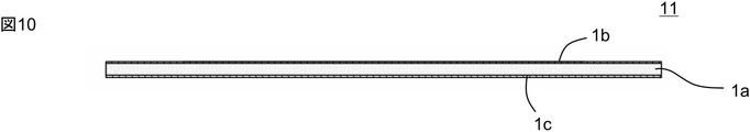
- 1 is a cross-sectional view showing a base sheet 11 of one embodiment of the present invention;
- Adhesive Sheet 10 An adhesive sheet 10 according to an embodiment of the present invention will be described with reference to FIGS. 1 to 9.
- FIG. The pressure-sensitive adhesive sheet 10 of this embodiment includes a base layer 1 and a pressure-sensitive adhesive layer 2 provided on the base layer 1 .
- This adhesive sheet 10 is used when grinding the back surface 4 b of the semiconductor wafer 4 having the projections 5 . Each configuration will be described below.
- the base material layer 1 includes a cushion layer 1a, a surface treatment layer 1b, and a barrier layer 1c.
- the surface treatment layer 1b is provided on the cushion layer 1a.
- the barrier layer 1c is preferably provided on the side opposite to the surface treatment layer 1b (or the adhesive layer 2) when viewed from the cushion layer 1a.
- the barrier layer 1c is preferably attached to the cushion layer 1a via an adhesive layer (not shown).
- the barrier layer 1c can be omitted.
- the thickness of the entire substrate layer 1 is preferably 50-400 ⁇ m, more preferably 100-350 ⁇ m, and even more preferably 200-300 ⁇ m. Specifically, the thickness is, for example, 50, 100, 150, 200, 250, 300, 350, 400 ⁇ m, and may be within a range between any two of the numerical values exemplified here.
- the cushion layer 1a is a layer for protecting the projections 5 of the semiconductor wafer 4 shown in FIG.
- the cushion layer 1a is preferably made of a thermoplastic resin.
- the composition of the thermoplastic resin is not particularly limited, but may be an ethylene-methacrylic acid-acrylic acid ester terpolymer, an ethylene-methacrylic acid copolymer, an ethylene-acrylic acid copolymer, etc., and/or a composite.
- styrene-butadiene copolymer rubber styrene-butadiene-styrene block copolymer rubber, styrene-isoprene-styrene block copolymer with polypropylene resin Rubber, soft polypropylene resin blended with ethylene-propylene rubber, etc., low-density polyethylene, ethylene-propylene block copolymer, ethylene-propylene random copolymer, ethylene-vinyl acetate copolymer, ethylene-methacrylic acid copolymer, Ethylene-1 octene copolymer, polybutene, etc. can be used. Among them, ionomer resin is preferable.
- the ratio Ra (% by mass) of the (meth)acrylic monomer unit in the resin constituting the cushion layer 1a is the ratio Rb (% by mass) of the (meth)acrylic monomer unit in the acrylic resin constituting the surface treatment layer 1b.
- the value of (Rb-Ra) is, for example, 10 to 100% by mass, preferably 30 to 100% by mass. Specifically, this value is, for example, 10, 20, 30, 40, 50, 60, 70, 80, 90, 100% by mass, and is within the range between any two of the numerical values exemplified here. may
- the storage elastic modulus E'a of the cushion layer 1a at 180°C is preferably lower than the storage elastic modulus E'b of the surface treatment layer 1b at 180°C.
- the storage elastic modulus E'a of the cushion layer 1a under high temperature conditions is low, the cushion layer 1a is excessively softened during heating, and the problem that the cushion layer 1a strongly adheres to the wafer and becomes difficult to peel off easily occurs.
- the storage elastic modulus E'a is lower than the storage elastic modulus E'b, the technical significance of providing the surface treatment layer 1b is significant.
- the storage elastic modulus E'a cannot be measured due to melting of the cushion layer 1a, the storage elastic modulus E'a is set to 0 for convenience.
- the weight average molecular weight (Mw) of the thermoplastic resin is preferably 10,000 to 1,000,000, more preferably 50,000 to 500,000.
- the weight average molecular weight (Mw) is a polystyrene-equivalent value measured by gel permeation chromatography (GPC).
- the softening temperature (JIS K7206) of the thermoplastic resin is preferably 45-200°C, more preferably 55-150°C. Specifically, this softening temperature is, for example, °C and may range between any two of the values exemplified herein.
- the melting point (JIS K7121) of the thermoplastic resin is preferably 60-200°C, more preferably 80-150°C.
- the melting points are, for example, 60, 70, 80, 90, 100, 110, 120, 130, 140, 150, 160, 170, 180, 190, and 200°C. or within a range between the two.
- the melt flow rate (MFR) JIS K7210, 125°C/10.0 kg load
- MFR melt flow rate
- the cushion layer 1a is moderately softened as the substrate layer 1 is heated, so that the projections 5 are easily embedded in the substrate layer 1.
- the thickness of the cushion layer 1a is preferably 50-400 ⁇ m, more preferably 100-350 ⁇ m, and even more preferably 200-300 ⁇ m. Specifically, the thickness is, for example, 50, 100, 150, 200, 250, 300, 350, 400 ⁇ m, and may be within a range between any two of the numerical values exemplified here.
- the surface treatment layer 1b is formed of an acrylic resin composition containing an acrylic resin, and is crosslinked by light irradiation or heating.
- the pressure-sensitive adhesive layer 2 may peel off if the adhesion between the cushion layer 1a and the pressure-sensitive adhesive layer 2 is not good. Peeling of the adhesive layer 2 can be suppressed by forming the surface treatment layer 1b on the substrate and then forming the adhesive layer 2 with an acrylic resin composition.
- the surface treatment layer 1b is formed on the cushion layer 1a, and the surface treatment layer 1b is attached to the semiconductor wafer.
- the surface-treated layer 1b has excellent adhesion to the pressure-sensitive adhesive layer 2 without being subjected to corona discharge treatment. Therefore, the surface-treated layer 1b does not need to be subjected to corona discharge treatment. Therefore, by providing the surface treatment layer 1b, it is possible to reduce the adhesive force between the substrate layer 1 and the semiconductor wafer.
- the semiconductor wafer to which the base layer 1 of the test piece cut out from the adhesive sheet 10 is bonded is heated in an atmosphere of 100 ° C. for 1 minute, and after cooling to room temperature
- the adhesive strength between the base material layer 1 and the semiconductor wafer at 23° C. measured according to JIS Z0237 can be less than 6 N/200 mm.
- the adhesive force between the substrate layer 1 and the semiconductor wafer is preferably smaller than the adhesive force between the adhesive layer 2 and the semiconductor wafer.
- This adhesive strength is, for example, 0 to 5.9 N/200 mm, more preferably 0.1 to 3 N/200 mm, even more preferably 0.5 to 2 N/200 mm.
- this adhesive strength is, for example, 0, 0.1, specifically, for example, 0.5, 1.0, 1.5, 2.0, 2.5, 3.0, 3.5 , 4.0, 4.5, 5.0, 5.5, 5.9 N/200 mm, and may be in the range between any two of the values exemplified herein.
- the adhesive force under the above measurement conditions before heating is preferably 5 N/200 mm or less.
- This adhesive force is, for example, 0 to 5 N/200 mm, specifically, for example, 0, 0.1, 0.5, 1, 2, 3, 4, 5 N/200 mm. It may be in the range between any two.
- a (meth)acrylic monomer means a compound having a (meth)acryloyl group.
- the (meth)acrylic monomer is preferably monofunctional.
- (Meth)acrylic monomers include, for example, (meth)acrylic acid and/or (meth)acrylic acid esters.
- (Meth)acrylic acid esters include alkyl (meth)acrylates, hydroxyalkyl (meth)acrylates, and (meth)acrylates having a cyclic ether skeleton. These may be used singly or in combination of two or more.
- alkyl (meth)acrylate a (meth)acrylate represented by the following general formula (A) is preferable.
- alkyl (meth)acrylates include methyl (meth)acrylate, ethyl (meth)acrylate, propyl (meth)acrylate, 2-ethylhexyl (meth)acrylate, isopropyl (meth)acrylate, butyl (meth)acrylate. , isobutyl (meth)acrylate, isooctyl (meth)acrylate, isononyl (meth)acrylate, lauryl (meth)acrylate, dodecyl (meth)acrylate and the like.
- Hydroxyalkyl (meth)acrylates include 2-hydroxypropyl (meth)acrylate, 2-hydroxybutyl (meth)acrylate, 2-hydroxyethyl (meth)acrylate and glycerol mono(meth)acrylate.
- Examples of (meth)acrylates having a cyclic ether skeleton include glycidyl (meth)acrylate, furfuryl (meth)acrylate, tetrahydrofurfuryl (meth)acrylate, 3-ethyl-3-oxetanylmethyl (meth)acrylate, (2-methyl- ethyl-1,3-dioxolan-4-yl)methyl (meth)acrylate, cyclic trimethylolpropane formal (meth)acrylate, ⁇ -butyrolactone (meth)acrylate, dioxolane (meth)acrylate, dioxane glycol di(meth)acrylate, oxetane (meth)acrylate and the like.
- cyclic ether skeletons 5- to 6-membered rings are preferred.
- the cyclic ether skeleton preferably has one oxygen atom.
- the cyclic ether skeleton preferably has 2 to 5 carbon atoms.
- (meth)acrylates having a cyclic ether skeleton glycidyl (meth)acrylate is preferred.
- the acrylic resin may contain only (meth)acrylic monomer units, or may contain monomer units other than (meth)acrylic monomer units.
- Other monomer units include olefins such as ethylene and propylene, aliphatic vinyls such as vinyl acetate, and aromatic vinyls such as styrene.
- the ratio of the (meth)acrylic monomer unit in the acrylic resin constituting the surface treatment layer 1b is, for example, 50 to 100% by mass, specifically, for example, 50, 55, 60, 65, 70, 75, 80, 85, 90, 95, 100% by mass, and may be within a range between any two of the numerical values exemplified here.
- the acrylic resin can be obtained by polymerizing a monomer mixture containing the above monomers.
- the acrylic resin composition preferably contains a cross-linking agent.
- the acrylic resin is crosslinked by the reaction between the acrylic resin and the crosslinking agent.
- cross-linking agents include acrylate-based cross-linking agents, isocyanate-based cross-linking agents, epoxy-based cross-linking agents, and amine-based cross-linking agents. These may be used alone or in combination of two or more.
- acrylate-based cross-linking agents include compounds having multiple (eg, two) (meth)acryloyl groups, and specific examples include 1,9-nonanediol diacrylate, 1,6-hexanediol diacrylate, triethylene glycol diacrylate, polytetramethylene glycol diacrylate, neopentyl glycol diacrylate, 3-methyl-1,5-pentanediol diacrylate and the like.
- isocyanate cross-linking agents examples include 2,4-tolylene diisocyanate, 2,6-tolylene diisocyanate, 1,3-xylylene diisocyanate, 1,4-xylylene diisocyanate, diphenylmethane-4,4′-diisocyanate, diphenylmethane -2,4'-diisocyanate, 3-methyldiphenylmethane diisocyanate, hexamethylene diisocyanate, isophorone diisocyanate, dicyclohexylmethane-4,4'-diisocyanate, dicyclohexylmethane-2,4'-diisocyanate, polyvalent isocyanate compounds such as lysine isocyanate, and derivatives thereof (adducts, burettes, isocyanurates) and the like. These may be used alone or in combination of two or more.
- the amount of the cross-linking agent added to 100 parts by mass of the acrylic resin is, for example, 0.5 to 30 parts by mass, preferably 4 to 25 parts by mass, and more preferably 7 to 20 parts by mass. Specifically, this amount is, for example, 0.5, 1, 2, 3, 4, 5, 6, 7, 8, 9, 10, 15, 20, 25, 30 parts by mass. It may be in a range between any two of the numbers given.
- Acrylic resin is crosslinked by light irradiation or heating.
- the acrylic resin composition preferably contains a photopolymerization initiator.
- a photopolymerization initiator include, but are not limited to, benzoin ether-based photopolymerization initiators, acetophenone-based photopolymerization initiators, ⁇ -ketol-based photopolymerization initiators, aromatic sulfonyl chloride-based photopolymerization initiators, and photopolymerization initiators.
- Active oxime photoinitiators benzoin photoinitiators, benzyl photoinitiators, benzophenone photoinitiators, ketal photoinitiators, thioxanthone photoinitiators, acylphosphine oxide photoinitiators
- An initiator or the like can be used, and an acetophenone-based photopolymerization initiator is preferred.
- acetophenone photopolymerization initiators include 1-hydroxycyclohexylphenyl ketone, 4-phenoxydichloroacetophenone, 4-t-butyl-dichloroacetophenone, 1-[4-(2-hydroxyethoxy)-phenyl]-2 -hydroxy-2-methyl-1-propan-1-one, 2-hydroxy-2-methyl-1-phenyl-propan-1-one, methoxyacetophenone and the like.
- the acrylic resin preferably has an Mw of 300,000 to 2,000,000, more preferably 450,000 to 800,000 before cross-linking. If the Mw is too low, the heat resistance may be insufficient, and if the Mw is too high, the viscosity will be too high and coating will be difficult, resulting in a decrease in productivity.
- Mw is, for example, 300,000, 350,000, 400,000, 450,000, 500,000, 550,000, 600,000, 650,000, 700,000, 750,000, 800,000, 900,000, 1,000,000, 1,100,000 , 1.2 million, 1.3 million, 1.4 million, 1.5 million, 1.6 million, 1.7 million, 1.8 million, 1.9 million, 2 million, and may be in a range between any two of the numbers exemplified herein.
- the acrylic resin preferably has a glass transition temperature (Tg) of -15 to 40°C before cross-linking, more preferably -10 to 30°C. Specifically, this Tg is, for example, ⁇ 15, ⁇ 10, ⁇ 5, 0, 5, 10, 15, 20, 25, 30, 35, 40° C. Any two of the numerical values exemplified here It may be in the range between.
- the Tg of the acrylic resin after cross-linking is preferably 10 to 80°C, more preferably 20 to 70°C. Specifically, this Tg is, for example, 10, 15, 20, 25, 30, 35, 40, 45, 50, 55, 60, 65, 70, 75, 80 ° C. Any of the numerical values exemplified here or within a range between the two.
- Tg is measured as follows. Differential scanning calorimetry (DSC) is measured according to JIS K 7121:1987. Let Tg be the intersection point of the tangent line of the baseline in the DSC curve and the tangent line of the steeply descending position of the endothermic region due to the glass transition.
- DSC Differential scanning calorimetry
- the surface treatment layer 1b preferably has a storage elastic modulus of 1.0 ⁇ 10 4 Pa to 1.0 ⁇ 10 8 Pa at 180°C. If the storage elastic modulus is too low, the surface treatment layer 1b becomes too soft when the adhesive sheet 10 is heated when the wafer is attached to the adhesive sheet 10. may be broken, leaving a residue of the surface treatment layer 1b on the wafer or impairing the releasability. If the storage elastic modulus is too high, the surface treatment layer 1b is too hard, and the conformability to the protrusions 5 of the base material layer 1 may deteriorate.
- the storage elastic modulus is, for example, 1.0 ⁇ 10 4 Pa, 1.0 ⁇ 10 5 Pa, 1.0 ⁇ 10 6 Pa, 1.0 ⁇ 10 7 Pa, 1.0 ⁇ 10 8 Pa and may be in a range between any two of the values exemplified here.
- the thickness of the surface treatment layer 1b is, for example, 0.1 to 10 ⁇ m, preferably 0.5 to 5 ⁇ m, more preferably 1 to 4 ⁇ m. When the surface treatment layer 1b has such a thickness, the effect of providing the surface treatment layer 1b tends to be exhibited appropriately. Specifically, this thickness is, for example, 0.1, 0.5, 1.0, 1.5, 2.0, 2.5, 3.0, 3.5, 4.0, 5.0 , 6.0, 7.0, 8.0, 9.0, 10.0 ⁇ m, and may be in the range between any two of the values exemplified herein.
- the barrier layer 1c is a layer for reducing the oxygen permeability of the substrate layer 1. As shown in FIG. If the base material layer 1 is easily permeable to air, outside air enters the closed space 2b through the base material layer 1, making it difficult to reduce the pressure in the closed space 2b. A problem that it becomes difficult to follow 5 may occur.
- the barrier layer 1c is a layer with low oxygen permeability. When the oxygen permeability is low, the air permeability is also generally low. can easily follow the convex portion 5.
- the barrier layer 1c should be provided so that the oxygen permeability of the base material layer 1 at 25° C. RH 0% measured according to JIS K 7162-2 (isobaric method) is 1000 ml/(m 2 24 h atm) or less. is preferred.
- the oxygen permeability of the barrier layer 1c alone under the same conditions is preferably 1000 ml/(m2.24 h.atm) or less. In this case, the above effects are likely to be exhibited.
- the oxygen permeability of the substrate layer 1 or the barrier layer 1c is, for example, 0 to 1000 ml/(m 2 ⁇ 24 h ⁇ atm), preferably 0 to 500 ml/(m 2 ⁇ 24 h ⁇ atm). , 0, 100, 200, 300, 400, 500, 600, 700, 800, 900, 1000 ml/(m 2 ⁇ 24 h ⁇ atm) and within the range between any two of the values exemplified here may
- the oxygen permeability of the barrier layer 1c is preferably lower than that of the cushion layer 1a.
- the value of (oxygen permeability of the cushion layer 1a ⁇ oxygen permeability of the barrier layer 1c) is preferably 100 ml/(m 2 ⁇ 24 h ⁇ atm) or more. This value is, for example, 100 to 3000 ml/(m 2 ⁇ 24 h ⁇ atm), specifically, for example, 100, 500, 1000, 1500, 2000, 2500, 3000 ml/(m 2 ⁇ 24 h ⁇ atm). , within a range between any two of the numerical values exemplified herein.
- the barrier layer 1c can be made of any material that can achieve the oxygen permeability described above, and polyester (eg, polyethylene terephthalate), polyimide, and polyamide are preferable from the viewpoint of easily lowering the oxygen permeability.
- polyester eg, polyethylene terephthalate
- polyimide polyimide
- polyamide polyamide
- the thickness of the barrier layer 1c is, for example, 5-50 ⁇ m, preferably 10-30 ⁇ m. If the barrier layer 1c is too thin, the oxygen permeability of the substrate layer 1 may not be sufficiently low. If the barrier layer 1c is too thick, the conformability to the protrusions 5 of the base material layer 1 may deteriorate. Specifically, the thickness is, for example, 5, 10, 15, 20, 25, 30, 35, 40, 45, 50 ⁇ m, and is within the range between any two of the numerical values exemplified here. good too.
- the adhesive layer 2 is a layer for attaching the adhesive sheet 10 to the semiconductor wafer 4, and is made of an adhesive.
- the shape of the adhesive layer 2 has an opening 2a with a smaller diameter than the diameter of the semiconductor wafer 4 . That is, the adhesive layer 2 is annular.
- the opening 2a is a portion where no adhesive is provided and has a smaller diameter than the diameter of the semiconductor wafer 4. As shown in FIG.
- the diameter of the opening 2a/the diameter of the semiconductor wafer 4 is preferably 0.950 to 0.995, more preferably 0.960 to 0.990.
- the outer peripheral portion 4a of the semiconductor wafer 4 is adhered to the adhesive layer 2 so that the projections 5 of the semiconductor wafer 4 are arranged in the openings 2a. For this reason, since the protrusions 5 do not come into contact with the adhesive, adhesive residue on the protrusions 5 is prevented.
- the width of the adhesive layer 2 is preferably 10-100 mm, more preferably 30-70 mm.
- the thickness of the adhesive layer 2 is preferably 1-100 ⁇ m, more preferably 5-50 ⁇ m. Specifically, the thickness is, for example, 1, 5, 10, 15, 20, 25, 30, 35, 40, 45, 50, 100 ⁇ m, and ranges between any two of the numerical values exemplified here. may be within
- the adhesive layer 2 is made of an acrylic resin composition containing an acrylic resin.
- the acrylic resin of the pressure-sensitive adhesive layer 2 may or may not have the same composition as the acrylic resin of the surface treatment layer 1b.
- the proportion of (meth)acrylic monomer units contained in the acrylic resin constituting the pressure-sensitive adhesive layer 2 is, for example, 50 to 100% by mass, specifically, for example, 50, 55, 60, 65, 70, 75. , 80, 85, 90, 95, 100 mass %, and may be within a range between any two of the numerical values exemplified here.
- (Meth)acrylic monomers include, for example, butyl (meth)acrylate, 2-butyl (meth)acrylate, t-butyl (meth)acrylate, pentyl (meth)acrylate, octyl (meth)acrylate, 2-ethylhexyl (meth) acrylate, nonyl (meth)acrylate, decyl (meth)acrylate, lauryl (meth)acrylate, methyl (meth)acrylate, ethyl (meth)acrylate, isopropyl (meth)acrylate, tridecyl (meth)acrylate, myristyl (meth)acrylate, (Meth)acrylic monomers and functional groups such as cetyl (meth)acrylate, stearyl (meth)acrylate, cyclohexyl (meth)acrylate, benzyl (meth)acrylate, dimethylacrylamide, diethylacrylamide, acryloylmorpho
- 2-hydroxyethyl (meth) acrylate, 2-hydroxypropyl (meth) acrylate, and 2-hydroxybutyl (meth) acrylate having a hydroxyl group (meth) acrylic acid having a carboxyl group, croton acid, maleic acid, itaconic acid, fumaric acid, acrylamido-N-glycolic acid, cinnamic acid and the like, allyl glycidyl ether having an epoxy group, glycidyl ether (meth)acrylic acid, and the like.
- a cross-linking agent is preferably added to the acrylic resin composition that constitutes the pressure-sensitive adhesive layer 2 .
- cross-linking agents include polyfunctional isocyanate cross-linking agents and polyfunctional epoxy cross-linking agents.
- 1,2-polybutadiene-terminated urethane (meth)acrylate, the hydrogenated product, 1,4-polybutadiene-terminated urethane (meth)acrylate, polyisoprene-terminated (meth)acrylate, polyester-based urethane (meth)acrylate, polyether-based (Meth)acrylate obtained by (meth)acrylating one or more oligomers/polymers such as urethane (meth)acrylate, polyester (meth)acrylate, bis-A type epoxy (meth)acrylate at the end or side chain may be used.
- the amount of the cross-linking agent added to 100 parts by mass of the acrylic resin is, for example, 0.1 to 10 parts by mass, preferably 0.5 to 8 parts by mass, more preferably 1 to 6 parts by mass.
- this compounding amount is, for example, 0.1, 0.5, 1.0, 1.5, 2.0, 2.5, 3.0, 3.5, 4.0, 4.5 , 5.0, 5.5, 6.0, 6.5, 7.0, 7.5, 8.0, 8.5, 9.0, 9.5, 10.0 parts by mass, where may be within a range between any two of the numerical values exemplified in .
- the glass transition temperature (Tg) of the acrylic resin after cross-linking is preferably -30 to 5°C, more preferably -25 to -5°C.
- This Tg is specifically, for example, -30, -25, -20, -15, -10, -5, 0, 5 ° C., within the range between any two of the numerical values illustrated here There may be.
- the pressure-sensitive adhesive layer 2 is formed by coating the pressure-sensitive adhesive on the base layer 1 or by applying a pressure-sensitive adhesive onto the release film by a coating method such as common comma coating, gravure coating, roll coating, or screen coating. It can be formed by applying to the substrate layer 1 and transferring it to the substrate layer 1 .
- the semiconductor wafer to which the adhesive layer 2 is attached is heated in an atmosphere of 100°C for 1 minute, and after cooling to room temperature, the adhesive strength between the adhesive layer 2 and the semiconductor wafer measured at 23°C according to JIS Z0237 is , 6 to 50 N/200 mm, preferably 10 to 30 N/200 mm. Also, the adhesive strength under the above measurement conditions before heating is preferably 6 N/200 mm or more, for example, 6 to 50 N/200 mm. These adhesive strengths are specifically, for example, 6, 10, 15, 20, 25, 30, 35, 40, 45, 50 N / 200 mm, and within the range between any two of the numerical values illustrated here may be
- a semiconductor wafer 4 has a convex portion 5 .
- the convex portion 5 is an arbitrary structure that protrudes in the out-of-plane direction of the semiconductor wafer 4 .
- Examples of the convex portion 5 include a projecting electrode and a convex portion of a circuit having unevenness.
- Examples of the semiconductor wafer 4 include not only silicon wafers, but also germanium wafers, gallium-arsenide wafers, gallium-phosphorus wafers, gallium-arsenide-aluminum wafers, and the like.
- the diameter of the semiconductor wafer 4 is preferably 1-16 inches, preferably 4-12 inches.
- the thickness of the semiconductor wafer 4 is not particularly limited, but is preferably 500-800 ⁇ m, more preferably 520-775 ⁇ m.
- the height of the projections 5 is preferably 10-500 ⁇ m, more preferably 100-300 ⁇ m. Specifically, this height is, for example, 10, 50, 100, 150, 200, 250, 300, 350, 400, 450, 500 ⁇ m, and within the range between any two of the numerical values exemplified here There may be.
- the semiconductor wafer 4 has an outer peripheral portion 4a on which the convex portion 5 is not provided.
- the width of the outer peripheral portion 4a is preferably 1.0 to 3.0 mm, more preferably 1.5 to 2.5 mm.
- Final products using the semiconductor wafer 4 having the projections 5 include electronic parts for logic, memory, sensor, power supply, and the like.
- the curable resin 8 is a resin that is cured by stimulation such as energy rays (eg, ultraviolet rays) or heat.
- a curable resin 8 is arranged between the substrate layer 1 and the support film 7 .
- the curable resin 8 preferably has a viscosity of 100 to 3000 mPa ⁇ s before curing, more preferably 200 to 1000 mPa ⁇ s.
- the viscosity is 100 mPa ⁇ s or more, the curable resin 8 is in point contact instead of surface contact, which suppresses the inclusion of air bubbles in the pressing process, resulting in excellent grindability.
- the viscosity is 3000 mPa ⁇ s or less, air bubbles are less likely to be involved when the curable resin 8 flows between the adjacent protrusions 5, resulting in excellent grindability.
- the viscosity is measured using an E-type viscometer under conditions of 23° C. and 50 rpm.
- the curable resin 8 preferably has a Shore D hardness of 5 to 70 after curing, more preferably 10 to 60.
- Shore D hardness is 5 or more, the grindability is excellent because the retention of the projections 5 is high.
- Shore D hardness is 70 or less, the adhesive sheet 10 tends to be curved when the adhesive sheet 10 is separated from the semiconductor wafer 4 .
- Shore D hardness is measured under conditions conforming to JIS K 6253.
- the curable resin 8 is preferably a photocurable resin, more preferably an ultraviolet curable resin.
- the curable resin 8 is preferably based on an acrylic resin, and its composition is not particularly limited.
- a synthetic resin is preferable because it can improve the adhesiveness between the substrate layer 1 and the support film 7 .
- the curing shrinkage rate of the curable resin 8 is preferably 7% or less.
- the thickness of the curable resin 8 is preferably (Td+20) to (Td+200) ⁇ m, more preferably (Td+50) to (Td+150) ⁇ m.
- the support film 7 is an arbitrary film capable of supporting the curable resin 8, and includes polyolefins such as ethylene vinyl acetate, polyethylene, polypropylene, polybutene, and polybutadiene, as well as polyvinyl chloride, polyethylene terephthalate, polyethylene naphthalate, polystyrene, It can be made of polycarbonate, polyimide, or the like.
- the thickness of the support film 7 is preferably 10-300 ⁇ m, more preferably 30-250 ⁇ m.
- FIG. 1 A method for manufacturing a semiconductor wafer using the adhesive sheet 10 will be described with reference to FIGS. 1 to 9.
- FIG. This manufacturing method includes a frame attaching process, a heating process, a cutting process, a resin curing process, a grinding process, and a peeling process.
- the order of performing these steps is not limited to this order, and the order can be changed as appropriate. Each step will be described below.
- an adhesive sheet 10 is attached to the ring frame 3 .
- the ring frame 3 has an opening 3 a with a diameter larger than the opening 2 a of the adhesive layer 2 , so that the ring frame 3 can be attached to the adhesive layer 2 .
- the adhesive sheet 10 is stably held on the ring frame 3, and the handling of the adhesive sheet 10 is facilitated.
- the adhesive sheet 10 is attached to the outer peripheral portion 4a of the semiconductor wafer 4 under reduced pressure on the surface of the semiconductor wafer 4 on which the protrusions 5 are provided.
- the width of the bonding surface where the semiconductor wafer 4 is bonded to the adhesive layer 2 is preferably 1.0 to 3.0 mm, more preferably 1.5 to 2.5 mm.
- the pressure in the decompression chamber 16 may be lower than the atmospheric pressure, preferably 1000 Pa or less, more preferably 500 Pa or less, and even more preferably 100 Pa or less. Although the lower limit of the pressure inside the decompression chamber 16 is not particularly specified, it is 10 Pa, for example.
- the base material layer 1 is pushed by the atmospheric pressure and tries to enter the sealed space 2b.
- the base material layer 1 has high rigidity in a non-heated state, and the base material layer 1 hardly enters the closed space 2b.
- the heating step when the substrate layer 1 is heated to 60 to 150° C., the substrate layer 1 is softened, and as shown in FIG. 4, the substrate layer 1 enters the sealed space 2b. Therefore, the protrusions 5 are embedded in the base layer 1 and are protected by the base layer 1 .
- the ratio of the height of the portion where the protrusion 5 is embedded/the height of the entire protrusion 5 is preferably 0.2 to 1, more preferably 0.5 to 1, and even more preferably 0.8 to 1.
- the heating temperature of the substrate layer 1 is preferably 80 to 120.degree.
- the heating time of the substrate layer 1 is preferably 3 to 120 seconds, more preferably 5 to 60 seconds.
- the heating of the base material layer 1 may be performed before or after the semiconductor wafer 4 is attached to the adhesive sheet 10 . Moreover, this heating may be performed within the decompression chamber 16 or may be performed outside the decompression chamber 16 .
- the adhesive sheet 10 is cut along the outer periphery of the semiconductor wafer 4. As shown in FIG. As a result, the adhesive sheet 10 to which the semiconductor wafer 4 is attached is separated from the ring frame 3 .
- the cutting step may be performed after the resin curing step.
- ⁇ Resin curing step> In the resin curing process, the base material layer 1 is brought into contact with the curable resin 8 after the wafer bonding process, and the curable resin 8 is cured in this state.
- This step can be carried out, for example, by the following method.
- the curable resin 8 is spread by moving the adhesive sheet 10 with the adhesive sheet 10 facing the curable resin 8 supplied on the support film 7 .
- the semiconductor wafer 4 is adsorbed to the decompression unit 6 having decompression holes 6a, and the adhesive sheet 10 is pressed against the curable resin 8 in that state.
- the curable resin 8 is spread by moving the adhesive sheet 10 along the surface of the support film 7 .
- the curable resin 8 is cured while the base material layer 1 is in contact with the curable resin 8.
- the curable resin 8 is cured while the base material layer 1 is in contact with the curable resin 8.
- the curable resin 8 can be cured into the curable resin 18 by irradiating the curable resin 8 with energy rays 9 such as ultraviolet rays through the support film 7 .
- energy rays 9 such as ultraviolet rays
- the adhesive sheet 10 is stably held on the support film 7 .
- the back surface 4b of the semiconductor wafer 4 is the surface opposite to the surface on which the projections 5 are provided.
- the method of grinding the back surface of the wafer is not particularly limited, and a known grinding method is adopted. Grinding is preferably carried out while cooling the wafer and grindstone (diamond or the like) with water.
- the thickness of the thinned wafer is preferably 300 ⁇ m or less, more preferably 50 ⁇ m or less.
- the projections 5 are easily damaged.
- the projections 5 are formed by the base layer 1 and the cured curable resin 8. Since it is stably supported, the convex portion 5 is less likely to be damaged.
- the adhesive sheet 10 is peeled off from the semiconductor wafer 4 in the peeling process.
- the adhesive sheet 10 can be peeled off by bending the adhesive sheet 10 in a direction away from the semiconductor wafer 4 .
- a dicing process may be performed before the peeling process.
- the semiconductor wafer 4 is divided into a plurality of semiconductor chips by dicing the semiconductor wafer 4 .
- the dicing method is not particularly limited, and may be any method such as blade dicing, laser dicing, stealth dicing, and plasma dicing.
- the peeling step is a step of peeling off each of the plurality of semiconductor chips from the adhesive sheet 10 .
- the base sheet 11 of one embodiment of the present invention can have the same configuration as the base layer 1 described above. That is, the base sheet 11 includes a cushion layer 1a and a surface-treated layer 1b provided thereon.
- the surface-treated layer 1b is formed of an acrylic resin composition containing an acrylic resin. Crosslinked by irradiation or heating.
- the base sheet 11 may include a barrier layer 1c.
- the description of the base material layer 1, the cushion layer 1a, the surface treatment layer 1b, and the barrier layer 1c is the same as in "1-1. Base material layer 1".
- the base sheet 11 can be used as the base layer 1 of the pressure-sensitive adhesive sheet 10 for grinding the back surface of the semiconductor wafer 4 having the protrusions 5 .
- the substrate sheet 11 may be used as a sheet for grinding the back surface of the semiconductor wafer 4 having the protrusions 5 without providing the adhesive layer 2 thereon.
- the base sheet 11 By removing the base sheet 11 and the semiconductor wafer 4 from the decompression chamber 16 after reducing the pressure inside, the base sheet 11 can be brought into close contact with the semiconductor wafer 4 by the action of atmospheric pressure.
- an annular packing having the same shape as the adhesive layer 2 may be arranged between the base sheet 11 and the semiconductor wafer 4.
- Example 1 Production of adhesive sheet 10 ⁇ Example 1>
- the pressure-sensitive adhesive sheet 10 was manufactured by forming the surface treatment layer 1b on the cushion layer 1a and forming the annular pressure-sensitive adhesive layer 2 having the openings 2a on the surface treatment layer 1b.
- a cushion layer 1a composed of a 150 ⁇ m-thick ethylene-methacrylic acid copolymer metal ion crosslinked product (Fanclare HMD manufactured by Gunze) was prepared.
- the ethylene-methacrylic acid copolymer had a methacrylic acid unit ratio of 15% by mass, an MFR (JIS K7210, 125°C/10.0 kg load) of 5 g/10 min, and a melting point (JIS K7121) of 72°C.
- ⁇ Formation of surface treatment layer 1b An acrylic copolymer containing 80 parts by mass of ethyl acrylate, 12 parts by mass of methyl methacrylate, 5 parts by mass of 2-hydroxyethyl methacrylate, and 3 parts by mass of glycidyl methacrylate as constituent monomers is polymerized, and this acrylic By adding 12 parts by weight of a cross-linking agent (Kyoeisha Chemical, Light Acrylate 1.9ND-A) to 100 parts by weight of the system copolymer and a photopolymerization initiator (OMNIRAT 184 manufactured by BASF) by 1 part by weight, A surface treatment agent was prepared.
- the acrylic copolymer had an Mw of 600,000 and a Tg of -7°C before cross-linking, and a Tg of 32°C after cross-linking.
- a surface treatment agent was coated on the cushion layer 1a and UV irradiation was performed to form a surface treatment layer 1b with a thickness of 2 ⁇ m.
- Example 2 A pressure-sensitive adhesive sheet 10 was produced in the same manner as in Example 1, except that the surface treatment layer 1b was formed after the cushion layer 1a was subjected to corona discharge treatment.
- Example 3 A pressure-sensitive adhesive sheet 10 was produced in the same manner as in Example 1, except that the surface treatment layer 1b was formed by the method described below.
- ⁇ Formation of surface treatment layer 1b An acrylic copolymer containing 50 parts by mass of ethyl acrylate, 42 parts by mass of methyl methacrylate, 5 parts by mass of 2-hydroxyethyl methacrylate, and 3 parts by mass of glycidyl methacrylate as constituent monomers is polymerized, and this acrylic A surface treatment agent was prepared by adding 2 parts by mass of an isocyanate cross-linking agent (Coronate L-45E, Nippon Polyurethane Co., Ltd.) to 100 parts by mass of the system copolymer.
- the acrylic copolymer had an Mw of 600,000 and a Tg of 24° C. before cross-linking, and a Tg of 61° C. after cross-linking.
- a surface treatment agent was coated on the cushion layer 1a and heated at 40°C for 7 days to form a surface treatment layer 1b with a thickness of 2 ⁇ m.
- Example 4 A pressure-sensitive adhesive sheet 10 was produced in the same manner as in Example 3, except that the surface treatment layer 1b was formed after the cushion layer 1a was subjected to corona discharge treatment.
- a pressure-sensitive adhesive sheet 10 was produced in the same manner as in Example 1, except that the pressure-sensitive adhesive layer 2 was formed on the cushion layer 1a without forming the surface treatment layer 1b.
- a pressure-sensitive adhesive sheet 10 was produced in the same manner as in Example 2, except that the pressure-sensitive adhesive layer 2 was formed on the cushion layer 1a without forming the surface treatment layer 1b.
- a pressure-sensitive adhesive sheet 10 was produced in the same manner as in Example 2, except that the surface treatment layer 1b was formed by the method described below.
- a pressure-sensitive adhesive sheet 10 was produced in the same manner as in Example 2, except that the pressure-sensitive adhesive layer 2 was formed by the method described below.
- Natural rubber 100 parts by mass, SIS (manufactured by Nippon Zeon, trade name “Quintac 3460C”, radial structure SIS, styrene content 25% by weight) 30 parts by mass, maleic anhydride After dissolving 40 parts by mass of acid-modified C5, C9 resin (manufactured by Nippon Zeon Co., Ltd., trade name “Quinton D-200”) in toluene, aromatic isocyanate (manufactured by Nippon Polyurethane Co., Ltd., trade name “Coronate L”) is used as a cross-linking agent.
- a rubber-based pressure-sensitive adhesive composition in the form of a solution. This composition was coated on a separator and cured by heating to obtain a pressure-sensitive adhesive film with a thickness of 10 ⁇ m. The pressure-sensitive adhesive film thus obtained was punched into a shape having openings, and the pressure-sensitive adhesive layer 2 having a thickness of 10 ⁇ m was formed in an annular shape by laminating it on the surface treatment layer.
- the pressure-sensitive adhesive sheet 10 was attached to the surface of the semiconductor wafer 4 on which the protrusions 5 were provided, on the outer peripheral portion 4a of the semiconductor wafer 4 within the decompression chamber 16 .
- a semiconductor wafer 4 having a diameter of 8 inches, a thickness of 725 ⁇ m, and bumps (protruding electrodes) having a height of 230 ⁇ m was formed in a region other than the outer circumference of 3.0 mm.
- the width of the bonding surface where the semiconductor wafer 4 is bonded to the adhesive layer 2 was 2.0 mm.
- the pressure inside the decompression chamber 16 was 100 Pa.
- the substrate layer 1 was heated to 100° C. in the decompression chamber 16 .
- the curable resin 8 was spread by moving the adhesive sheet 10 in the in-plane direction of the support film 7 while the adhesive sheet 10 faced the curable resin 8 supplied on the support film 7 .
- the curable resin 8 used was composed of 1,2-hydrogenated polybutadiene-terminated urethane (meth)acrylate, isobornyl acrylate, and diethylacrylamide.
- the viscosity of the curable resin 8 before curing was 470 mPa ⁇ s.
- the curable resin 8 was cured while the substrate layer 1 was in contact with the curable resin 8 to form a cured resin 18 .
- the curable resin 8 was cured by irradiating the curable resin with ultraviolet light from the support film 7 side so that the integrated amount of light with a wavelength of 365 nm was 2000 mJ/cm 2 .
- the Shore D hardness (JIS K 6253) of the cured resin 18 was 15.
- Bump followability was evaluated from the follow-up rate according to the following criteria. ⁇ (excellent): follow-up rate of 70% or more ⁇ (improper): follow-up rate of less than 70%
- ⁇ Adhesion between cushion layer and surface treatment layer> After cross-cutting the surface treatment layer 1b formed on the cushion layer 1a (100 squares of 1 mm 2 ) in a grid pattern, a JIS Z 1522 compliant cellophane adhesive tape (manufactured by Nichiban Co., Ltd.) was applied to the surface treatment layer. After sticking it on 1b and strongly pressing it with a finger, it was peeled off in the direction of 90°, and the presence or absence of peeling of the surface treatment layer 1b was evaluated. ⁇ (excellent): no peeling ⁇ (improper): peeling
- the adhesive strength between the substrate layer and the wafer was measured by the following method. A test piece having a width of 10 mm and a length of 100 mm is cut out from a portion near the center of the adhesive sheet 10 where the adhesive layer 2 is not formed (that is, a portion where the base layer is exposed), and this test piece is used. , JIS Z0237 (2009) for measuring adhesive strength (method 1: a test method in which a tape and a sheet are peeled off from a stainless steel test plate at 180°).
- a test piece was pressed onto an adherend (Si wafer) whose surface was cleaned using a pressing device (roller weight: 2 kg), and then heated on a hot plate at 100° C. for 1 minute.
- the adhesive strength when the test piece is peeled off at 180 ° from the adherend is measured in an environment with a temperature of 23 ° C and a humidity of 50% with a universal tensile tester (Tensilon model number: RTG-1210 manufactured by ORIENTEC).
- the measurement results measured under the following conditions were converted into numerical values at a width of 200 mm.
- Measurement mode Tensile Tensile speed: 300mm/min Distance between chucks: 50mm
- Measurement sample width 10 mm
- the peelability between the substrate layer and the wafer was evaluated according to the following criteria. ⁇ (excellent): 0.5 to 50N/200mm ⁇ (impossible): more than 50N/200mm
Landscapes
- Chemical & Material Sciences (AREA)
- Engineering & Computer Science (AREA)
- Organic Chemistry (AREA)
- Microelectronics & Electronic Packaging (AREA)
- Condensed Matter Physics & Semiconductors (AREA)
- General Physics & Mathematics (AREA)
- Manufacturing & Machinery (AREA)
- Computer Hardware Design (AREA)
- Physics & Mathematics (AREA)
- Power Engineering (AREA)
- Chemical Kinetics & Catalysis (AREA)
- Life Sciences & Earth Sciences (AREA)
- Materials Engineering (AREA)
- Wood Science & Technology (AREA)
- Adhesive Tapes (AREA)
- Mechanical Treatment Of Semiconductor (AREA)
- Adhesives Or Adhesive Processes (AREA)
Abstract
Priority Applications (4)
| Application Number | Priority Date | Filing Date | Title |
|---|---|---|---|
| KR1020237044784A KR20240013216A (ko) | 2021-05-26 | 2022-05-11 | 이면 연삭용 점착 시트 및 반도체 웨이퍼의 제조 방법, 기재 시트 |
| JP2023523404A JPWO2022249888A1 (fr) | 2021-05-26 | 2022-05-11 | |
| EP22811161.3A EP4333025A1 (fr) | 2021-05-26 | 2022-05-11 | Feuille adhésive pour meulage de surface arrière, procédé de fabrication de tranche semi-conductrice et feuille de matériau de base |
| CN202280037383.2A CN117378035A (zh) | 2021-05-26 | 2022-05-11 | 背面研磨用粘着片及半导体晶圆的制造方法、基材片 |
Applications Claiming Priority (2)
| Application Number | Priority Date | Filing Date | Title |
|---|---|---|---|
| JP2021088684 | 2021-05-26 | ||
| JP2021-088684 | 2021-05-26 |
Publications (1)
| Publication Number | Publication Date |
|---|---|
| WO2022249888A1 true WO2022249888A1 (fr) | 2022-12-01 |
Family
ID=84229872
Family Applications (1)
| Application Number | Title | Priority Date | Filing Date |
|---|---|---|---|
| PCT/JP2022/019981 WO2022249888A1 (fr) | 2021-05-26 | 2022-05-11 | Feuille adhésive pour meulage de surface arrière, procédé de fabrication de tranche semi-conductrice et feuille de matériau de base |
Country Status (6)
| Country | Link |
|---|---|
| EP (1) | EP4333025A1 (fr) |
| JP (1) | JPWO2022249888A1 (fr) |
| KR (1) | KR20240013216A (fr) |
| CN (1) | CN117378035A (fr) |
| TW (1) | TW202248390A (fr) |
| WO (1) | WO2022249888A1 (fr) |
Citations (6)
| Publication number | Priority date | Publication date | Assignee | Title |
|---|---|---|---|---|
| JP2010174067A (ja) * | 2009-01-27 | 2010-08-12 | Furukawa Electric Co Ltd:The | 表面保護用粘着テープ |
| JP2012216619A (ja) * | 2011-03-31 | 2012-11-08 | Lintec Corp | 表面保護用シート |
| JP2013211439A (ja) * | 2012-03-30 | 2013-10-10 | Lintec Corp | 表面保護用シート |
| JP2018526826A (ja) * | 2015-08-31 | 2018-09-13 | プリーヴァッサー, カール ハインツPRIEWASSER, Karl Heinz | ウェーハを処理する方法および該方法で使用するための保護シート |
| JP2019140387A (ja) | 2018-02-14 | 2019-08-22 | 株式会社ディスコ | ウェハの処理方法 |
| JP2020024976A (ja) * | 2018-08-06 | 2020-02-13 | 株式会社ディスコ | 保護部材形成装置 |
-
2022
- 2022-05-11 CN CN202280037383.2A patent/CN117378035A/zh active Pending
- 2022-05-11 WO PCT/JP2022/019981 patent/WO2022249888A1/fr active Application Filing
- 2022-05-11 EP EP22811161.3A patent/EP4333025A1/fr active Pending
- 2022-05-11 KR KR1020237044784A patent/KR20240013216A/ko unknown
- 2022-05-11 JP JP2023523404A patent/JPWO2022249888A1/ja active Pending
- 2022-05-23 TW TW111119040A patent/TW202248390A/zh unknown
Patent Citations (6)
| Publication number | Priority date | Publication date | Assignee | Title |
|---|---|---|---|---|
| JP2010174067A (ja) * | 2009-01-27 | 2010-08-12 | Furukawa Electric Co Ltd:The | 表面保護用粘着テープ |
| JP2012216619A (ja) * | 2011-03-31 | 2012-11-08 | Lintec Corp | 表面保護用シート |
| JP2013211439A (ja) * | 2012-03-30 | 2013-10-10 | Lintec Corp | 表面保護用シート |
| JP2018526826A (ja) * | 2015-08-31 | 2018-09-13 | プリーヴァッサー, カール ハインツPRIEWASSER, Karl Heinz | ウェーハを処理する方法および該方法で使用するための保護シート |
| JP2019140387A (ja) | 2018-02-14 | 2019-08-22 | 株式会社ディスコ | ウェハの処理方法 |
| JP2020024976A (ja) * | 2018-08-06 | 2020-02-13 | 株式会社ディスコ | 保護部材形成装置 |
Also Published As
| Publication number | Publication date |
|---|---|
| CN117378035A (zh) | 2024-01-09 |
| JPWO2022249888A1 (fr) | 2022-12-01 |
| TW202248390A (zh) | 2022-12-16 |
| KR20240013216A (ko) | 2024-01-30 |
| EP4333025A1 (fr) | 2024-03-06 |
Similar Documents
| Publication | Publication Date | Title |
|---|---|---|
| JP4369584B2 (ja) | 半導体ウエハ保持保護用粘着シート | |
| JP6539336B2 (ja) | 半導体加工用シートおよび半導体装置の製造方法 | |
| KR102544301B1 (ko) | 수지막 형성용 시트 적층체 | |
| JP2008143924A (ja) | 再剥離型粘着剤組成物、及び粘着テープ又はシート | |
| JP6306362B2 (ja) | 伸長可能シートおよび積層チップの製造方法 | |
| US20110008597A1 (en) | Surface protective sheet | |
| TW202016234A (zh) | 半導體加工用黏著帶及半導體裝置的製造方法 | |
| TW202020096A (zh) | 半導體加工用黏著帶及半導體裝置的製造方法 | |
| JP5414953B1 (ja) | ダイシングシートおよびデバイスチップの製造方法 | |
| JP6009188B2 (ja) | ワーク加工用シート基材およびワーク加工用シート | |
| WO2013141251A1 (fr) | Film, substrat en feuille pour le traitement d'une pièce et feuille pour le traitement d'une pièce | |
| JPWO2019181730A1 (ja) | 粘着テープおよび半導体装置の製造方法 | |
| JP6207192B2 (ja) | 半導体加工用粘着シート | |
| JP4947564B2 (ja) | 半導体ウエハ加工用粘着シート | |
| JPWO2015141555A1 (ja) | ダイシングシートおよび当該ダイシングシートを用いるチップの製造方法 | |
| JPWO2015141555A6 (ja) | ダイシングシートおよび当該ダイシングシートを用いるチップの製造方法 | |
| JP5546232B2 (ja) | 感圧型半導体ウエハ表面保護用粘着テープ | |
| WO2022249888A1 (fr) | Feuille adhésive pour meulage de surface arrière, procédé de fabrication de tranche semi-conductrice et feuille de matériau de base | |
| WO2022249889A1 (fr) | Feuille adhésive pour meulage arrière, procédé de fabrication de tranche semi-conductrice et feuille de substrat | |
| JP2017165880A (ja) | 半導体加工用シート | |
| JP6343725B2 (ja) | 半導体加工シート用基材フィルムおよび半導体加工シート | |
| WO2020175364A1 (fr) | Feuille adhésive d'affûtage de dos et procédé de fabrication d'un semi-conducteur étagé | |
| JP6087122B2 (ja) | ダイシングシート | |
| JP6190134B2 (ja) | ダイシングシート用基材フィルム、ダイシングシート、ダイシングシート用基材フィルムの製造方法およびチップ状部材の製造方法 | |
| WO2022209119A1 (fr) | Bande adhésive de traitement de semi-conducteur et procédé de fabrication de dispositif à semi-conducteur |
Legal Events
| Date | Code | Title | Description |
|---|---|---|---|
| 121 | Ep: the epo has been informed by wipo that ep was designated in this application |
Ref document number: 22811161 Country of ref document: EP Kind code of ref document: A1 |
|
| WWE | Wipo information: entry into national phase |
Ref document number: 2023523404 Country of ref document: JP |
|
| WWE | Wipo information: entry into national phase |
Ref document number: 18559745 Country of ref document: US |
|
| WWE | Wipo information: entry into national phase |
Ref document number: 202280037383.2 Country of ref document: CN |
|
| WWE | Wipo information: entry into national phase |
Ref document number: 2022811161 Country of ref document: EP |
|
| ENP | Entry into the national phase |
Ref document number: 2022811161 Country of ref document: EP Effective date: 20231129 |
|
| ENP | Entry into the national phase |
Ref document number: 20237044784 Country of ref document: KR Kind code of ref document: A |
|
| WWE | Wipo information: entry into national phase |
Ref document number: 1020237044784 Country of ref document: KR |
|
| NENP | Non-entry into the national phase |
Ref country code: DE |