WO2022249888A1 - Adhesive sheet for rear surface grinding, semiconductor wafer manufacturing method, and base material sheet - Google Patents
Adhesive sheet for rear surface grinding, semiconductor wafer manufacturing method, and base material sheet Download PDFInfo
- Publication number
- WO2022249888A1 WO2022249888A1 PCT/JP2022/019981 JP2022019981W WO2022249888A1 WO 2022249888 A1 WO2022249888 A1 WO 2022249888A1 JP 2022019981 W JP2022019981 W JP 2022019981W WO 2022249888 A1 WO2022249888 A1 WO 2022249888A1
- Authority
- WO
- WIPO (PCT)
- Prior art keywords
- layer
- semiconductor wafer
- adhesive sheet
- pressure
- sensitive adhesive
- Prior art date
Links
- 239000004065 semiconductor Substances 0.000 title claims abstract description 119
- 239000000853 adhesive Substances 0.000 title claims abstract description 106
- 230000001070 adhesive effect Effects 0.000 title claims abstract description 106
- 239000000463 material Substances 0.000 title claims abstract description 35
- 238000000227 grinding Methods 0.000 title claims abstract description 27
- 238000004519 manufacturing process Methods 0.000 title claims description 10
- 239000010410 layer Substances 0.000 claims abstract description 198
- 239000002335 surface treatment layer Substances 0.000 claims abstract description 68
- 239000004925 Acrylic resin Substances 0.000 claims abstract description 49
- 229920000178 Acrylic resin Polymers 0.000 claims abstract description 49
- 239000012790 adhesive layer Substances 0.000 claims abstract description 46
- 238000010438 heat treatment Methods 0.000 claims abstract description 26
- 239000000203 mixture Substances 0.000 claims abstract description 24
- 239000004820 Pressure-sensitive adhesive Substances 0.000 claims description 73
- 229920005989 resin Polymers 0.000 claims description 64
- 239000011347 resin Substances 0.000 claims description 64
- 238000000034 method Methods 0.000 claims description 49
- 239000000758 substrate Substances 0.000 claims description 35
- 230000008569 process Effects 0.000 claims description 29
- 238000003860 storage Methods 0.000 claims description 17
- 238000005520 cutting process Methods 0.000 claims description 11
- 230000002093 peripheral effect Effects 0.000 claims description 9
- 238000012360 testing method Methods 0.000 claims description 9
- 239000012298 atmosphere Substances 0.000 claims description 4
- 238000001816 cooling Methods 0.000 claims description 4
- 235000012431 wafers Nutrition 0.000 description 126
- NIXOWILDQLNWCW-UHFFFAOYSA-M Acrylate Chemical compound [O-]C(=O)C=C NIXOWILDQLNWCW-UHFFFAOYSA-M 0.000 description 61
- -1 polypropylene Polymers 0.000 description 25
- 239000003431 cross linking reagent Substances 0.000 description 20
- 230000006837 decompression Effects 0.000 description 20
- 239000000178 monomer Substances 0.000 description 20
- 230000004888 barrier function Effects 0.000 description 19
- NIXOWILDQLNWCW-UHFFFAOYSA-N acrylic acid group Chemical group C(C=C)(=O)O NIXOWILDQLNWCW-UHFFFAOYSA-N 0.000 description 15
- 230000035699 permeability Effects 0.000 description 14
- 229910052760 oxygen Inorganic materials 0.000 description 13
- 239000001301 oxygen Substances 0.000 description 13
- QVGXLLKOCUKJST-UHFFFAOYSA-N atomic oxygen Chemical compound [O] QVGXLLKOCUKJST-UHFFFAOYSA-N 0.000 description 12
- 239000003999 initiator Substances 0.000 description 12
- 238000003851 corona treatment Methods 0.000 description 10
- 230000000052 comparative effect Effects 0.000 description 9
- 238000004132 cross linking Methods 0.000 description 9
- 239000012948 isocyanate Substances 0.000 description 8
- 150000001252 acrylic acid derivatives Chemical class 0.000 description 7
- 238000005259 measurement Methods 0.000 description 7
- 229920005992 thermoplastic resin Polymers 0.000 description 7
- KWOLFJPFCHCOCG-UHFFFAOYSA-N Acetophenone Chemical compound CC(=O)C1=CC=CC=C1 KWOLFJPFCHCOCG-UHFFFAOYSA-N 0.000 description 6
- 238000000576 coating method Methods 0.000 description 6
- 150000004292 cyclic ethers Chemical group 0.000 description 6
- 239000012756 surface treatment agent Substances 0.000 description 6
- JOYRKODLDBILNP-UHFFFAOYSA-N Ethyl urethane Chemical compound CCOC(N)=O JOYRKODLDBILNP-UHFFFAOYSA-N 0.000 description 5
- CERQOIWHTDAKMF-UHFFFAOYSA-N Methacrylic acid Chemical compound CC(=C)C(O)=O CERQOIWHTDAKMF-UHFFFAOYSA-N 0.000 description 5
- 229920006243 acrylic copolymer Polymers 0.000 description 5
- 230000015572 biosynthetic process Effects 0.000 description 5
- 239000011248 coating agent Substances 0.000 description 5
- 150000002513 isocyanates Chemical class 0.000 description 5
- PPBRXRYQALVLMV-UHFFFAOYSA-N Styrene Chemical compound C=CC1=CC=CC=C1 PPBRXRYQALVLMV-UHFFFAOYSA-N 0.000 description 4
- 125000000217 alkyl group Chemical group 0.000 description 4
- 229920001971 elastomer Polymers 0.000 description 4
- 229920005648 ethylene methacrylic acid copolymer Polymers 0.000 description 4
- 238000011156 evaluation Methods 0.000 description 4
- 238000002844 melting Methods 0.000 description 4
- 230000008018 melting Effects 0.000 description 4
- 238000003825 pressing Methods 0.000 description 4
- 239000005060 rubber Substances 0.000 description 4
- 239000004593 Epoxy Substances 0.000 description 3
- JIGUQPWFLRLWPJ-UHFFFAOYSA-N Ethyl acrylate Chemical compound CCOC(=O)C=C JIGUQPWFLRLWPJ-UHFFFAOYSA-N 0.000 description 3
- LYCAIKOWRPUZTN-UHFFFAOYSA-N Ethylene glycol Chemical compound OCCO LYCAIKOWRPUZTN-UHFFFAOYSA-N 0.000 description 3
- WOBHKFSMXKNTIM-UHFFFAOYSA-N Hydroxyethyl methacrylate Chemical compound CC(=C)C(=O)OCCO WOBHKFSMXKNTIM-UHFFFAOYSA-N 0.000 description 3
- VVQNEPGJFQJSBK-UHFFFAOYSA-N Methyl methacrylate Chemical compound COC(=O)C(C)=C VVQNEPGJFQJSBK-UHFFFAOYSA-N 0.000 description 3
- 239000004743 Polypropylene Substances 0.000 description 3
- YXFVVABEGXRONW-UHFFFAOYSA-N Toluene Chemical compound CC1=CC=CC=C1 YXFVVABEGXRONW-UHFFFAOYSA-N 0.000 description 3
- 125000003647 acryloyl group Chemical group O=C([*])C([H])=C([H])[H] 0.000 description 3
- 239000000470 constituent Substances 0.000 description 3
- 229920001577 copolymer Polymers 0.000 description 3
- 125000003438 dodecyl group Chemical group [H]C([H])([H])C([H])([H])C([H])([H])C([H])([H])C([H])([H])C([H])([H])C([H])([H])C([H])([H])C([H])([H])C([H])([H])C([H])([H])C([H])([H])* 0.000 description 3
- 125000000524 functional group Chemical group 0.000 description 3
- 230000009477 glass transition Effects 0.000 description 3
- VOZRXNHHFUQHIL-UHFFFAOYSA-N glycidyl methacrylate Chemical compound CC(=C)C(=O)OCC1CO1 VOZRXNHHFUQHIL-UHFFFAOYSA-N 0.000 description 3
- PNJWIWWMYCMZRO-UHFFFAOYSA-N pent‐4‐en‐2‐one Natural products CC(=O)CC=C PNJWIWWMYCMZRO-UHFFFAOYSA-N 0.000 description 3
- 229920000728 polyester Polymers 0.000 description 3
- 229920000139 polyethylene terephthalate Polymers 0.000 description 3
- 239000005020 polyethylene terephthalate Substances 0.000 description 3
- 229920001155 polypropylene Polymers 0.000 description 3
- 229920000346 polystyrene-polyisoprene block-polystyrene Polymers 0.000 description 3
- PSGCQDPCAWOCSH-UHFFFAOYSA-N (4,7,7-trimethyl-3-bicyclo[2.2.1]heptanyl) prop-2-enoate Chemical compound C1CC2(C)C(OC(=O)C=C)CC1C2(C)C PSGCQDPCAWOCSH-UHFFFAOYSA-N 0.000 description 2
- INQDDHNZXOAFFD-UHFFFAOYSA-N 2-[2-(2-prop-2-enoyloxyethoxy)ethoxy]ethyl prop-2-enoate Chemical compound C=CC(=O)OCCOCCOCCOC(=O)C=C INQDDHNZXOAFFD-UHFFFAOYSA-N 0.000 description 2
- 125000000954 2-hydroxyethyl group Chemical group [H]C([*])([H])C([H])([H])O[H] 0.000 description 2
- UVRCNEIYXSRHNT-UHFFFAOYSA-N 3-ethylpent-2-enamide Chemical compound CCC(CC)=CC(N)=O UVRCNEIYXSRHNT-UHFFFAOYSA-N 0.000 description 2
- YEJRWHAVMIAJKC-UHFFFAOYSA-N 4-Butyrolactone Chemical compound O=C1CCCO1 YEJRWHAVMIAJKC-UHFFFAOYSA-N 0.000 description 2
- VZCYOOQTPOCHFL-OWOJBTEDSA-N Fumaric acid Chemical compound OC(=O)\C=C\C(O)=O VZCYOOQTPOCHFL-OWOJBTEDSA-N 0.000 description 2
- 244000043261 Hevea brasiliensis Species 0.000 description 2
- 239000005062 Polybutadiene Substances 0.000 description 2
- 239000004642 Polyimide Substances 0.000 description 2
- XUIMIQQOPSSXEZ-UHFFFAOYSA-N Silicon Chemical compound [Si] XUIMIQQOPSSXEZ-UHFFFAOYSA-N 0.000 description 2
- ISAOCJYIOMOJEB-UHFFFAOYSA-N benzoin Chemical compound C=1C=CC=CC=1C(O)C(=O)C1=CC=CC=C1 ISAOCJYIOMOJEB-UHFFFAOYSA-N 0.000 description 2
- 125000001797 benzyl group Chemical group [H]C1=C([H])C([H])=C(C([H])=C1[H])C([H])([H])* 0.000 description 2
- 125000000484 butyl group Chemical group [H]C([*])([H])C([H])([H])C([H])([H])C([H])([H])[H] 0.000 description 2
- 125000004432 carbon atom Chemical group C* 0.000 description 2
- 125000003178 carboxy group Chemical group [H]OC(*)=O 0.000 description 2
- 150000001875 compounds Chemical class 0.000 description 2
- 230000000694 effects Effects 0.000 description 2
- 125000001495 ethyl group Chemical group [H]C([H])([H])C([H])([H])* 0.000 description 2
- 239000005038 ethylene vinyl acetate Substances 0.000 description 2
- 238000005227 gel permeation chromatography Methods 0.000 description 2
- 125000003055 glycidyl group Chemical group C(C1CO1)* 0.000 description 2
- WGCNASOHLSPBMP-UHFFFAOYSA-N hydroxyacetaldehyde Natural products OCC=O WGCNASOHLSPBMP-UHFFFAOYSA-N 0.000 description 2
- 125000002768 hydroxyalkyl group Chemical group 0.000 description 2
- 230000001678 irradiating effect Effects 0.000 description 2
- 125000001449 isopropyl group Chemical group [H]C([H])([H])C([H])(*)C([H])([H])[H] 0.000 description 2
- 229910021645 metal ion Inorganic materials 0.000 description 2
- 125000002496 methyl group Chemical group [H]C([H])([H])* 0.000 description 2
- 229920003052 natural elastomer Polymers 0.000 description 2
- 229920001194 natural rubber Polymers 0.000 description 2
- 229920001200 poly(ethylene-vinyl acetate) Polymers 0.000 description 2
- 229920002857 polybutadiene Polymers 0.000 description 2
- 229920001083 polybutene Polymers 0.000 description 2
- 229920001721 polyimide Polymers 0.000 description 2
- 229920000642 polymer Polymers 0.000 description 2
- 229920002635 polyurethane Polymers 0.000 description 2
- 238000012545 processing Methods 0.000 description 2
- 229910052710 silicon Inorganic materials 0.000 description 2
- 239000010703 silicon Substances 0.000 description 2
- 239000000126 substance Substances 0.000 description 2
- VZCYOOQTPOCHFL-UHFFFAOYSA-N trans-butenedioic acid Natural products OC(=O)C=CC(O)=O VZCYOOQTPOCHFL-UHFFFAOYSA-N 0.000 description 2
- 238000009281 ultraviolet germicidal irradiation Methods 0.000 description 2
- 229920002554 vinyl polymer Polymers 0.000 description 2
- IQGIEMYBDGDBMR-UHFFFAOYSA-N (3-methyl-5-prop-2-enoyloxypentyl) prop-2-enoate Chemical compound C=CC(=O)OCCC(C)CCOC(=O)C=C IQGIEMYBDGDBMR-UHFFFAOYSA-N 0.000 description 1
- WBYWAXJHAXSJNI-VOTSOKGWSA-M .beta-Phenylacrylic acid Natural products [O-]C(=O)\C=C\C1=CC=CC=C1 WBYWAXJHAXSJNI-VOTSOKGWSA-M 0.000 description 1
- JWTGRKUQJXIWCV-UHFFFAOYSA-N 1,2,3-trihydroxypropyl 2-methylprop-2-enoate Chemical compound CC(=C)C(=O)OC(O)C(O)CO JWTGRKUQJXIWCV-UHFFFAOYSA-N 0.000 description 1
- WNXJIVFYUVYPPR-UHFFFAOYSA-N 1,3-dioxolane Chemical compound C1COCO1 WNXJIVFYUVYPPR-UHFFFAOYSA-N 0.000 description 1
- RYHBNJHYFVUHQT-UHFFFAOYSA-N 1,4-Dioxane Chemical compound C1COCCO1 RYHBNJHYFVUHQT-UHFFFAOYSA-N 0.000 description 1
- OHLKMGYGBHFODF-UHFFFAOYSA-N 1,4-bis(isocyanatomethyl)benzene Chemical compound O=C=NCC1=CC=C(CN=C=O)C=C1 OHLKMGYGBHFODF-UHFFFAOYSA-N 0.000 description 1
- FWWWRCRHNMOYQY-UHFFFAOYSA-N 1,5-diisocyanato-2,4-dimethylbenzene Chemical compound CC1=CC(C)=C(N=C=O)C=C1N=C=O FWWWRCRHNMOYQY-UHFFFAOYSA-N 0.000 description 1
- 239000012956 1-hydroxycyclohexylphenyl-ketone Substances 0.000 description 1
- LFSYUSUFCBOHGU-UHFFFAOYSA-N 1-isocyanato-2-[(4-isocyanatophenyl)methyl]benzene Chemical compound C1=CC(N=C=O)=CC=C1CC1=CC=CC=C1N=C=O LFSYUSUFCBOHGU-UHFFFAOYSA-N 0.000 description 1
- XLPJNCYCZORXHG-UHFFFAOYSA-N 1-morpholin-4-ylprop-2-en-1-one Chemical compound C=CC(=O)N1CCOCC1 XLPJNCYCZORXHG-UHFFFAOYSA-N 0.000 description 1
- STMDPCBYJCIZOD-UHFFFAOYSA-N 2-(2,4-dinitroanilino)-4-methylpentanoic acid Chemical compound CC(C)CC(C(O)=O)NC1=CC=C([N+]([O-])=O)C=C1[N+]([O-])=O STMDPCBYJCIZOD-UHFFFAOYSA-N 0.000 description 1
- JAHNSTQSQJOJLO-UHFFFAOYSA-N 2-(3-fluorophenyl)-1h-imidazole Chemical compound FC1=CC=CC(C=2NC=CN=2)=C1 JAHNSTQSQJOJLO-UHFFFAOYSA-N 0.000 description 1
- GJKGAPPUXSSCFI-UHFFFAOYSA-N 2-Hydroxy-4'-(2-hydroxyethoxy)-2-methylpropiophenone Chemical compound CC(C)(O)C(=O)C1=CC=C(OCCO)C=C1 GJKGAPPUXSSCFI-UHFFFAOYSA-N 0.000 description 1
- NLGDWWCZQDIASO-UHFFFAOYSA-N 2-hydroxy-1-(7-oxabicyclo[4.1.0]hepta-1,3,5-trien-2-yl)-2-phenylethanone Chemical compound OC(C(=O)c1cccc2Oc12)c1ccccc1 NLGDWWCZQDIASO-UHFFFAOYSA-N 0.000 description 1
- XMLYCEVDHLAQEL-UHFFFAOYSA-N 2-hydroxy-2-methyl-1-phenylpropan-1-one Chemical compound CC(C)(O)C(=O)C1=CC=CC=C1 XMLYCEVDHLAQEL-UHFFFAOYSA-N 0.000 description 1
- YRNDGUSDBCARGC-UHFFFAOYSA-N 2-methoxyacetophenone Chemical compound COCC(=O)C1=CC=CC=C1 YRNDGUSDBCARGC-UHFFFAOYSA-N 0.000 description 1
- WHNPOQXWAMXPTA-UHFFFAOYSA-N 3-methylbut-2-enamide Chemical compound CC(C)=CC(N)=O WHNPOQXWAMXPTA-UHFFFAOYSA-N 0.000 description 1
- UPMLOUAZCHDJJD-UHFFFAOYSA-N 4,4'-Diphenylmethane Diisocyanate Chemical compound C1=CC(N=C=O)=CC=C1CC1=CC=C(N=C=O)C=C1 UPMLOUAZCHDJJD-UHFFFAOYSA-N 0.000 description 1
- FIHBHSQYSYVZQE-UHFFFAOYSA-N 6-prop-2-enoyloxyhexyl prop-2-enoate Chemical compound C=CC(=O)OCCCCCCOC(=O)C=C FIHBHSQYSYVZQE-UHFFFAOYSA-N 0.000 description 1
- LVGFPWDANALGOY-UHFFFAOYSA-N 8-methylnonyl prop-2-enoate Chemical compound CC(C)CCCCCCCOC(=O)C=C LVGFPWDANALGOY-UHFFFAOYSA-N 0.000 description 1
- PGDIJTMOHORACQ-UHFFFAOYSA-N 9-prop-2-enoyloxynonyl prop-2-enoate Chemical compound C=CC(=O)OCCCCCCCCCOC(=O)C=C PGDIJTMOHORACQ-UHFFFAOYSA-N 0.000 description 1
- JBRZTFJDHDCESZ-UHFFFAOYSA-N AsGa Chemical compound [As]#[Ga] JBRZTFJDHDCESZ-UHFFFAOYSA-N 0.000 description 1
- 229920000298 Cellophane Polymers 0.000 description 1
- WBYWAXJHAXSJNI-SREVYHEPSA-N Cinnamic acid Chemical compound OC(=O)\C=C/C1=CC=CC=C1 WBYWAXJHAXSJNI-SREVYHEPSA-N 0.000 description 1
- 244000168525 Croton tiglium Species 0.000 description 1
- SNRUBQQJIBEYMU-UHFFFAOYSA-N Dodecane Natural products CCCCCCCCCCCC SNRUBQQJIBEYMU-UHFFFAOYSA-N 0.000 description 1
- VGGSQFUCUMXWEO-UHFFFAOYSA-N Ethene Chemical compound C=C VGGSQFUCUMXWEO-UHFFFAOYSA-N 0.000 description 1
- 239000005977 Ethylene Substances 0.000 description 1
- 229920000181 Ethylene propylene rubber Polymers 0.000 description 1
- 229910001218 Gallium arsenide Inorganic materials 0.000 description 1
- 239000005057 Hexamethylene diisocyanate Substances 0.000 description 1
- 239000005058 Isophorone diisocyanate Substances 0.000 description 1
- HBBGRARXTFLTSG-UHFFFAOYSA-N Lithium ion Chemical compound [Li+] HBBGRARXTFLTSG-UHFFFAOYSA-N 0.000 description 1
- KDXKERNSBIXSRK-UHFFFAOYSA-N Lysine Natural products NCCCCC(N)C(O)=O KDXKERNSBIXSRK-UHFFFAOYSA-N 0.000 description 1
- 239000004472 Lysine Substances 0.000 description 1
- JLVVSXFLKOJNIY-UHFFFAOYSA-N Magnesium ion Chemical compound [Mg+2] JLVVSXFLKOJNIY-UHFFFAOYSA-N 0.000 description 1
- 239000004952 Polyamide Substances 0.000 description 1
- 239000004698 Polyethylene Substances 0.000 description 1
- 239000004721 Polyphenylene oxide Substances 0.000 description 1
- 239000004793 Polystyrene Substances 0.000 description 1
- OFOBLEOULBTSOW-UHFFFAOYSA-N Propanedioic acid Natural products OC(=O)CC(O)=O OFOBLEOULBTSOW-UHFFFAOYSA-N 0.000 description 1
- 244000028419 Styrax benzoin Species 0.000 description 1
- 235000000126 Styrax benzoin Nutrition 0.000 description 1
- 235000008411 Sumatra benzointree Nutrition 0.000 description 1
- ZJCCRDAZUWHFQH-UHFFFAOYSA-N Trimethylolpropane Chemical compound CCC(CO)(CO)CO ZJCCRDAZUWHFQH-UHFFFAOYSA-N 0.000 description 1
- XTXRWKRVRITETP-UHFFFAOYSA-N Vinyl acetate Chemical compound CC(=O)OC=C XTXRWKRVRITETP-UHFFFAOYSA-N 0.000 description 1
- QYKIQEUNHZKYBP-UHFFFAOYSA-N Vinyl ether Chemical compound C=COC=C QYKIQEUNHZKYBP-UHFFFAOYSA-N 0.000 description 1
- 239000002253 acid Substances 0.000 description 1
- 230000009471 action Effects 0.000 description 1
- 239000002390 adhesive tape Substances 0.000 description 1
- 150000001336 alkenes Chemical class 0.000 description 1
- 229910052782 aluminium Inorganic materials 0.000 description 1
- 150000001412 amines Chemical class 0.000 description 1
- 239000002518 antifoaming agent Substances 0.000 description 1
- 229920006272 aromatic hydrocarbon resin Polymers 0.000 description 1
- 125000003118 aryl group Chemical group 0.000 description 1
- 238000005452 bending Methods 0.000 description 1
- 229960002130 benzoin Drugs 0.000 description 1
- RWCCWEUUXYIKHB-UHFFFAOYSA-N benzophenone Chemical compound C=1C=CC=CC=1C(=O)C1=CC=CC=C1 RWCCWEUUXYIKHB-UHFFFAOYSA-N 0.000 description 1
- 239000012965 benzophenone Substances 0.000 description 1
- MQDJYUACMFCOFT-UHFFFAOYSA-N bis[2-(1-hydroxycyclohexyl)phenyl]methanone Chemical compound C=1C=CC=C(C(=O)C=2C(=CC=CC=2)C2(O)CCCCC2)C=1C1(O)CCCCC1 MQDJYUACMFCOFT-UHFFFAOYSA-N 0.000 description 1
- DQXBYHZEEUGOBF-UHFFFAOYSA-N but-3-enoic acid;ethene Chemical compound C=C.OC(=O)CC=C DQXBYHZEEUGOBF-UHFFFAOYSA-N 0.000 description 1
- 229930016911 cinnamic acid Natural products 0.000 description 1
- 235000013985 cinnamic acid Nutrition 0.000 description 1
- 239000002131 composite material Substances 0.000 description 1
- 238000013329 compounding Methods 0.000 description 1
- 125000004122 cyclic group Chemical group 0.000 description 1
- 125000000113 cyclohexyl group Chemical group [H]C1([H])C([H])([H])C([H])([H])C([H])(*)C([H])([H])C1([H])[H] 0.000 description 1
- 125000002704 decyl group Chemical group [H]C([H])([H])C([H])([H])C([H])([H])C([H])([H])C([H])([H])C([H])([H])C([H])([H])C([H])([H])C([H])([H])C([H])([H])* 0.000 description 1
- 230000006866 deterioration Effects 0.000 description 1
- 125000004386 diacrylate group Chemical group 0.000 description 1
- 229910003460 diamond Inorganic materials 0.000 description 1
- 239000010432 diamond Substances 0.000 description 1
- KORSJDCBLAPZEQ-UHFFFAOYSA-N dicyclohexylmethane-4,4'-diisocyanate Chemical compound C1CC(N=C=O)CCC1CC1CCC(N=C=O)CC1 KORSJDCBLAPZEQ-UHFFFAOYSA-N 0.000 description 1
- 238000000113 differential scanning calorimetry Methods 0.000 description 1
- 238000001938 differential scanning calorimetry curve Methods 0.000 description 1
- GYZLOYUZLJXAJU-UHFFFAOYSA-N diglycidyl ether Chemical compound C1OC1COCC1CO1 GYZLOYUZLJXAJU-UHFFFAOYSA-N 0.000 description 1
- BXKDSDJJOVIHMX-UHFFFAOYSA-N edrophonium chloride Chemical compound [Cl-].CC[N+](C)(C)C1=CC=CC(O)=C1 BXKDSDJJOVIHMX-UHFFFAOYSA-N 0.000 description 1
- 125000003700 epoxy group Chemical group 0.000 description 1
- 229920006242 ethylene acrylic acid copolymer Polymers 0.000 description 1
- 229920005676 ethylene-propylene block copolymer Polymers 0.000 description 1
- 229920005674 ethylene-propylene random copolymer Polymers 0.000 description 1
- 239000001530 fumaric acid Substances 0.000 description 1
- 229910052732 germanium Inorganic materials 0.000 description 1
- GNPVGFCGXDBREM-UHFFFAOYSA-N germanium atom Chemical compound [Ge] GNPVGFCGXDBREM-UHFFFAOYSA-N 0.000 description 1
- 238000007756 gravure coating Methods 0.000 description 1
- 235000019382 gum benzoic Nutrition 0.000 description 1
- RRAMGCGOFNQTLD-UHFFFAOYSA-N hexamethylene diisocyanate Chemical compound O=C=NCCCCCCN=C=O RRAMGCGOFNQTLD-UHFFFAOYSA-N 0.000 description 1
- 125000002887 hydroxy group Chemical group [H]O* 0.000 description 1
- 229920000554 ionomer Polymers 0.000 description 1
- 125000000959 isobutyl group Chemical group [H]C([H])([H])C([H])(C([H])([H])[H])C([H])([H])* 0.000 description 1
- NIMLQBUJDJZYEJ-UHFFFAOYSA-N isophorone diisocyanate Chemical compound CC1(C)CC(N=C=O)CC(C)(CN=C=O)C1 NIMLQBUJDJZYEJ-UHFFFAOYSA-N 0.000 description 1
- 238000010030 laminating Methods 0.000 description 1
- 239000007788 liquid Substances 0.000 description 1
- 229910001416 lithium ion Inorganic materials 0.000 description 1
- 229920001684 low density polyethylene Polymers 0.000 description 1
- 239000004702 low-density polyethylene Substances 0.000 description 1
- 229910001425 magnesium ion Inorganic materials 0.000 description 1
- 230000014759 maintenance of location Effects 0.000 description 1
- VZCYOOQTPOCHFL-UPHRSURJSA-N maleic acid Chemical compound OC(=O)\C=C/C(O)=O VZCYOOQTPOCHFL-UPHRSURJSA-N 0.000 description 1
- 239000011976 maleic acid Substances 0.000 description 1
- FPYJFEHAWHCUMM-UHFFFAOYSA-N maleic anhydride Chemical compound O=C1OC(=O)C=C1 FPYJFEHAWHCUMM-UHFFFAOYSA-N 0.000 description 1
- 239000000155 melt Substances 0.000 description 1
- 125000005395 methacrylic acid group Chemical group 0.000 description 1
- YDKNBNOOCSNPNS-UHFFFAOYSA-N methyl 1,3-benzoxazole-2-carboxylate Chemical compound C1=CC=C2OC(C(=O)OC)=NC2=C1 YDKNBNOOCSNPNS-UHFFFAOYSA-N 0.000 description 1
- WBYWAXJHAXSJNI-UHFFFAOYSA-N methyl p-hydroxycinnamate Natural products OC(=O)C=CC1=CC=CC=C1 WBYWAXJHAXSJNI-UHFFFAOYSA-N 0.000 description 1
- LVHBHZANLOWSRM-UHFFFAOYSA-N methylenebutanedioic acid Natural products OC(=O)CC(=C)C(O)=O LVHBHZANLOWSRM-UHFFFAOYSA-N 0.000 description 1
- 125000001421 myristyl group Chemical group [H]C([*])([H])C([H])([H])C([H])([H])C([H])([H])C([H])([H])C([H])([H])C([H])([H])C([H])([H])C([H])([H])C([H])([H])C([H])([H])C([H])([H])C([H])([H])C([H])([H])[H] 0.000 description 1
- CMWTZPSULFXXJA-VIFPVBQESA-N naproxen Chemical group C1=C([C@H](C)C(O)=O)C=CC2=CC(OC)=CC=C21 CMWTZPSULFXXJA-VIFPVBQESA-N 0.000 description 1
- 125000001400 nonyl group Chemical group [H]C([*])([H])C([H])([H])C([H])([H])C([H])([H])C([H])([H])C([H])([H])C([H])([H])C([H])([H])C([H])([H])[H] 0.000 description 1
- 125000002347 octyl group Chemical group [H]C([*])([H])C([H])([H])C([H])([H])C([H])([H])C([H])([H])C([H])([H])C([H])([H])C([H])([H])[H] 0.000 description 1
- AHHWIHXENZJRFG-UHFFFAOYSA-N oxetane Chemical compound C1COC1 AHHWIHXENZJRFG-UHFFFAOYSA-N 0.000 description 1
- 150000002923 oximes Chemical class 0.000 description 1
- 125000004430 oxygen atom Chemical group O* 0.000 description 1
- 238000012856 packing Methods 0.000 description 1
- 125000000913 palmityl group Chemical group [H]C([*])([H])C([H])([H])C([H])([H])C([H])([H])C([H])([H])C([H])([H])C([H])([H])C([H])([H])C([H])([H])C([H])([H])C([H])([H])C([H])([H])C([H])([H])C([H])([H])C([H])([H])C([H])([H])[H] 0.000 description 1
- 125000001147 pentyl group Chemical group C(CCCC)* 0.000 description 1
- 229910052698 phosphorus Inorganic materials 0.000 description 1
- 239000011574 phosphorus Substances 0.000 description 1
- 230000000704 physical effect Effects 0.000 description 1
- 229920003207 poly(ethylene-2,6-naphthalate) Polymers 0.000 description 1
- 229920002647 polyamide Polymers 0.000 description 1
- 239000004417 polycarbonate Substances 0.000 description 1
- 229920000515 polycarbonate Polymers 0.000 description 1
- 229920000570 polyether Polymers 0.000 description 1
- 229920000573 polyethylene Polymers 0.000 description 1
- 239000011112 polyethylene naphthalate Substances 0.000 description 1
- 230000000379 polymerizing effect Effects 0.000 description 1
- 229920000098 polyolefin Polymers 0.000 description 1
- 229920002223 polystyrene Polymers 0.000 description 1
- 239000004800 polyvinyl chloride Substances 0.000 description 1
- 229920000915 polyvinyl chloride Polymers 0.000 description 1
- 238000002360 preparation method Methods 0.000 description 1
- 125000001436 propyl group Chemical group [H]C([*])([H])C([H])([H])C([H])([H])[H] 0.000 description 1
- QQONPFPTGQHPMA-UHFFFAOYSA-N propylene Natural products CC=C QQONPFPTGQHPMA-UHFFFAOYSA-N 0.000 description 1
- 125000004805 propylene group Chemical group [H]C([H])([H])C([H])([*:1])C([H])([H])[*:2] 0.000 description 1
- 230000009993 protective function Effects 0.000 description 1
- 125000002914 sec-butyl group Chemical group [H]C([H])([H])C([H])([H])C([H])(*)C([H])([H])[H] 0.000 description 1
- 229910001415 sodium ion Inorganic materials 0.000 description 1
- 229910001220 stainless steel Inorganic materials 0.000 description 1
- 239000010935 stainless steel Substances 0.000 description 1
- 125000004079 stearyl group Chemical group [H]C([*])([H])C([H])([H])C([H])([H])C([H])([H])C([H])([H])C([H])([H])C([H])([H])C([H])([H])C([H])([H])C([H])([H])C([H])([H])C([H])([H])C([H])([H])C([H])([H])C([H])([H])C([H])([H])C([H])([H])C([H])([H])[H] 0.000 description 1
- 230000000638 stimulation Effects 0.000 description 1
- 229920003048 styrene butadiene rubber Polymers 0.000 description 1
- 229920000468 styrene butadiene styrene block copolymer Polymers 0.000 description 1
- YBBRCQOCSYXUOC-UHFFFAOYSA-N sulfuryl dichloride Chemical compound ClS(Cl)(=O)=O YBBRCQOCSYXUOC-UHFFFAOYSA-N 0.000 description 1
- 229920003002 synthetic resin Polymers 0.000 description 1
- 239000000057 synthetic resin Substances 0.000 description 1
- 229920001897 terpolymer Polymers 0.000 description 1
- 125000000999 tert-butyl group Chemical group [H]C([H])([H])C(*)(C([H])([H])[H])C([H])([H])[H] 0.000 description 1
- 238000010998 test method Methods 0.000 description 1
- YRHRIQCWCFGUEQ-UHFFFAOYSA-N thioxanthen-9-one Chemical compound C1=CC=C2C(=O)C3=CC=CC=C3SC2=C1 YRHRIQCWCFGUEQ-UHFFFAOYSA-N 0.000 description 1
- DVKJHBMWWAPEIU-UHFFFAOYSA-N toluene 2,4-diisocyanate Chemical compound CC1=CC=C(N=C=O)C=C1N=C=O DVKJHBMWWAPEIU-UHFFFAOYSA-N 0.000 description 1
- RUELTTOHQODFPA-UHFFFAOYSA-N toluene 2,6-diisocyanate Chemical compound CC1=C(N=C=O)C=CC=C1N=C=O RUELTTOHQODFPA-UHFFFAOYSA-N 0.000 description 1
- 125000002889 tridecyl group Chemical group [H]C([*])([H])C([H])([H])C([H])([H])C([H])([H])C([H])([H])C([H])([H])C([H])([H])C([H])([H])C([H])([H])C([H])([H])C([H])([H])C([H])([H])C([H])([H])[H] 0.000 description 1
- XLYOFNOQVPJJNP-UHFFFAOYSA-N water Substances O XLYOFNOQVPJJNP-UHFFFAOYSA-N 0.000 description 1
Images


Classifications
-
- H—ELECTRICITY
- H01—ELECTRIC ELEMENTS
- H01L—SEMICONDUCTOR DEVICES NOT COVERED BY CLASS H10
- H01L21/00—Processes or apparatus adapted for the manufacture or treatment of semiconductor or solid state devices or of parts thereof
- H01L21/67—Apparatus specially adapted for handling semiconductor or electric solid state devices during manufacture or treatment thereof; Apparatus specially adapted for handling wafers during manufacture or treatment of semiconductor or electric solid state devices or components ; Apparatus not specifically provided for elsewhere
- H01L21/683—Apparatus specially adapted for handling semiconductor or electric solid state devices during manufacture or treatment thereof; Apparatus specially adapted for handling wafers during manufacture or treatment of semiconductor or electric solid state devices or components ; Apparatus not specifically provided for elsewhere for supporting or gripping
- H01L21/6835—Apparatus specially adapted for handling semiconductor or electric solid state devices during manufacture or treatment thereof; Apparatus specially adapted for handling wafers during manufacture or treatment of semiconductor or electric solid state devices or components ; Apparatus not specifically provided for elsewhere for supporting or gripping using temporarily an auxiliary support
- H01L21/6836—Wafer tapes, e.g. grinding or dicing support tapes
-
- C—CHEMISTRY; METALLURGY
- C09—DYES; PAINTS; POLISHES; NATURAL RESINS; ADHESIVES; COMPOSITIONS NOT OTHERWISE PROVIDED FOR; APPLICATIONS OF MATERIALS NOT OTHERWISE PROVIDED FOR
- C09J—ADHESIVES; NON-MECHANICAL ASPECTS OF ADHESIVE PROCESSES IN GENERAL; ADHESIVE PROCESSES NOT PROVIDED FOR ELSEWHERE; USE OF MATERIALS AS ADHESIVES
- C09J7/00—Adhesives in the form of films or foils
- C09J7/20—Adhesives in the form of films or foils characterised by their carriers
-
- B—PERFORMING OPERATIONS; TRANSPORTING
- B32—LAYERED PRODUCTS
- B32B—LAYERED PRODUCTS, i.e. PRODUCTS BUILT-UP OF STRATA OF FLAT OR NON-FLAT, e.g. CELLULAR OR HONEYCOMB, FORM
- B32B27/00—Layered products comprising a layer of synthetic resin
-
- C—CHEMISTRY; METALLURGY
- C09—DYES; PAINTS; POLISHES; NATURAL RESINS; ADHESIVES; COMPOSITIONS NOT OTHERWISE PROVIDED FOR; APPLICATIONS OF MATERIALS NOT OTHERWISE PROVIDED FOR
- C09D—COATING COMPOSITIONS, e.g. PAINTS, VARNISHES OR LACQUERS; FILLING PASTES; CHEMICAL PAINT OR INK REMOVERS; INKS; CORRECTING FLUIDS; WOODSTAINS; PASTES OR SOLIDS FOR COLOURING OR PRINTING; USE OF MATERIALS THEREFOR
- C09D133/00—Coating compositions based on homopolymers or copolymers of compounds having one or more unsaturated aliphatic radicals, each having only one carbon-to-carbon double bond, and at least one being terminated by only one carboxyl radical, or of salts, anhydrides, esters, amides, imides, or nitriles thereof; Coating compositions based on derivatives of such polymers
-
- C—CHEMISTRY; METALLURGY
- C09—DYES; PAINTS; POLISHES; NATURAL RESINS; ADHESIVES; COMPOSITIONS NOT OTHERWISE PROVIDED FOR; APPLICATIONS OF MATERIALS NOT OTHERWISE PROVIDED FOR
- C09J—ADHESIVES; NON-MECHANICAL ASPECTS OF ADHESIVE PROCESSES IN GENERAL; ADHESIVE PROCESSES NOT PROVIDED FOR ELSEWHERE; USE OF MATERIALS AS ADHESIVES
- C09J133/00—Adhesives based on homopolymers or copolymers of compounds having one or more unsaturated aliphatic radicals, each having only one carbon-to-carbon double bond, and at least one being terminated by only one carboxyl radical, or of salts, anhydrides, esters, amides, imides, or nitriles thereof; Adhesives based on derivatives of such polymers
-
- C—CHEMISTRY; METALLURGY
- C09—DYES; PAINTS; POLISHES; NATURAL RESINS; ADHESIVES; COMPOSITIONS NOT OTHERWISE PROVIDED FOR; APPLICATIONS OF MATERIALS NOT OTHERWISE PROVIDED FOR
- C09J—ADHESIVES; NON-MECHANICAL ASPECTS OF ADHESIVE PROCESSES IN GENERAL; ADHESIVE PROCESSES NOT PROVIDED FOR ELSEWHERE; USE OF MATERIALS AS ADHESIVES
- C09J7/00—Adhesives in the form of films or foils
- C09J7/20—Adhesives in the form of films or foils characterised by their carriers
- C09J7/29—Laminated material
-
- C—CHEMISTRY; METALLURGY
- C09—DYES; PAINTS; POLISHES; NATURAL RESINS; ADHESIVES; COMPOSITIONS NOT OTHERWISE PROVIDED FOR; APPLICATIONS OF MATERIALS NOT OTHERWISE PROVIDED FOR
- C09J—ADHESIVES; NON-MECHANICAL ASPECTS OF ADHESIVE PROCESSES IN GENERAL; ADHESIVE PROCESSES NOT PROVIDED FOR ELSEWHERE; USE OF MATERIALS AS ADHESIVES
- C09J7/00—Adhesives in the form of films or foils
- C09J7/30—Adhesives in the form of films or foils characterised by the adhesive composition
- C09J7/38—Pressure-sensitive adhesives [PSA]
- C09J7/381—Pressure-sensitive adhesives [PSA] based on macromolecular compounds obtained by reactions involving only carbon-to-carbon unsaturated bonds
- C09J7/385—Acrylic polymers
-
- H—ELECTRICITY
- H01—ELECTRIC ELEMENTS
- H01L—SEMICONDUCTOR DEVICES NOT COVERED BY CLASS H10
- H01L21/00—Processes or apparatus adapted for the manufacture or treatment of semiconductor or solid state devices or of parts thereof
- H01L21/02—Manufacture or treatment of semiconductor devices or of parts thereof
- H01L21/04—Manufacture or treatment of semiconductor devices or of parts thereof the devices having at least one potential-jump barrier or surface barrier, e.g. PN junction, depletion layer or carrier concentration layer
- H01L21/18—Manufacture or treatment of semiconductor devices or of parts thereof the devices having at least one potential-jump barrier or surface barrier, e.g. PN junction, depletion layer or carrier concentration layer the devices having semiconductor bodies comprising elements of Group IV of the Periodic System or AIIIBV compounds with or without impurities, e.g. doping materials
- H01L21/30—Treatment of semiconductor bodies using processes or apparatus not provided for in groups H01L21/20 - H01L21/26
- H01L21/302—Treatment of semiconductor bodies using processes or apparatus not provided for in groups H01L21/20 - H01L21/26 to change their surface-physical characteristics or shape, e.g. etching, polishing, cutting
- H01L21/304—Mechanical treatment, e.g. grinding, polishing, cutting
-
- H—ELECTRICITY
- H01—ELECTRIC ELEMENTS
- H01L—SEMICONDUCTOR DEVICES NOT COVERED BY CLASS H10
- H01L21/00—Processes or apparatus adapted for the manufacture or treatment of semiconductor or solid state devices or of parts thereof
- H01L21/70—Manufacture or treatment of devices consisting of a plurality of solid state components formed in or on a common substrate or of parts thereof; Manufacture of integrated circuit devices or of parts thereof
- H01L21/77—Manufacture or treatment of devices consisting of a plurality of solid state components or integrated circuits formed in, or on, a common substrate
- H01L21/78—Manufacture or treatment of devices consisting of a plurality of solid state components or integrated circuits formed in, or on, a common substrate with subsequent division of the substrate into plural individual devices
-
- C—CHEMISTRY; METALLURGY
- C09—DYES; PAINTS; POLISHES; NATURAL RESINS; ADHESIVES; COMPOSITIONS NOT OTHERWISE PROVIDED FOR; APPLICATIONS OF MATERIALS NOT OTHERWISE PROVIDED FOR
- C09J—ADHESIVES; NON-MECHANICAL ASPECTS OF ADHESIVE PROCESSES IN GENERAL; ADHESIVE PROCESSES NOT PROVIDED FOR ELSEWHERE; USE OF MATERIALS AS ADHESIVES
- C09J2203/00—Applications of adhesives in processes or use of adhesives in the form of films or foils
- C09J2203/326—Applications of adhesives in processes or use of adhesives in the form of films or foils for bonding electronic components such as wafers, chips or semiconductors
-
- C—CHEMISTRY; METALLURGY
- C09—DYES; PAINTS; POLISHES; NATURAL RESINS; ADHESIVES; COMPOSITIONS NOT OTHERWISE PROVIDED FOR; APPLICATIONS OF MATERIALS NOT OTHERWISE PROVIDED FOR
- C09J—ADHESIVES; NON-MECHANICAL ASPECTS OF ADHESIVE PROCESSES IN GENERAL; ADHESIVE PROCESSES NOT PROVIDED FOR ELSEWHERE; USE OF MATERIALS AS ADHESIVES
- C09J2433/00—Presence of (meth)acrylic polymer
- C09J2433/001—Presence of (meth)acrylic polymer in the barrier layer
-
- H—ELECTRICITY
- H01—ELECTRIC ELEMENTS
- H01L—SEMICONDUCTOR DEVICES NOT COVERED BY CLASS H10
- H01L21/00—Processes or apparatus adapted for the manufacture or treatment of semiconductor or solid state devices or of parts thereof
- H01L21/67—Apparatus specially adapted for handling semiconductor or electric solid state devices during manufacture or treatment thereof; Apparatus specially adapted for handling wafers during manufacture or treatment of semiconductor or electric solid state devices or components ; Apparatus not specifically provided for elsewhere
- H01L21/67005—Apparatus not specifically provided for elsewhere
- H01L21/67011—Apparatus for manufacture or treatment
- H01L21/67132—Apparatus for placing on an insulating substrate, e.g. tape
-
- H—ELECTRICITY
- H01—ELECTRIC ELEMENTS
- H01L—SEMICONDUCTOR DEVICES NOT COVERED BY CLASS H10
- H01L2221/00—Processes or apparatus adapted for the manufacture or treatment of semiconductor or solid state devices or of parts thereof covered by H01L21/00
- H01L2221/67—Apparatus for handling semiconductor or electric solid state devices during manufacture or treatment thereof; Apparatus for handling wafers during manufacture or treatment of semiconductor or electric solid state devices or components; Apparatus not specifically provided for elsewhere
- H01L2221/683—Apparatus for handling semiconductor or electric solid state devices during manufacture or treatment thereof; Apparatus for handling wafers during manufacture or treatment of semiconductor or electric solid state devices or components; Apparatus not specifically provided for elsewhere for supporting or gripping
- H01L2221/68304—Apparatus for handling semiconductor or electric solid state devices during manufacture or treatment thereof; Apparatus for handling wafers during manufacture or treatment of semiconductor or electric solid state devices or components; Apparatus not specifically provided for elsewhere for supporting or gripping using temporarily an auxiliary support
- H01L2221/68327—Apparatus for handling semiconductor or electric solid state devices during manufacture or treatment thereof; Apparatus for handling wafers during manufacture or treatment of semiconductor or electric solid state devices or components; Apparatus not specifically provided for elsewhere for supporting or gripping using temporarily an auxiliary support used during dicing or grinding
-
- H—ELECTRICITY
- H01—ELECTRIC ELEMENTS
- H01L—SEMICONDUCTOR DEVICES NOT COVERED BY CLASS H10
- H01L2221/00—Processes or apparatus adapted for the manufacture or treatment of semiconductor or solid state devices or of parts thereof covered by H01L21/00
- H01L2221/67—Apparatus for handling semiconductor or electric solid state devices during manufacture or treatment thereof; Apparatus for handling wafers during manufacture or treatment of semiconductor or electric solid state devices or components; Apparatus not specifically provided for elsewhere
- H01L2221/683—Apparatus for handling semiconductor or electric solid state devices during manufacture or treatment thereof; Apparatus for handling wafers during manufacture or treatment of semiconductor or electric solid state devices or components; Apparatus not specifically provided for elsewhere for supporting or gripping
- H01L2221/68304—Apparatus for handling semiconductor or electric solid state devices during manufacture or treatment thereof; Apparatus for handling wafers during manufacture or treatment of semiconductor or electric solid state devices or components; Apparatus not specifically provided for elsewhere for supporting or gripping using temporarily an auxiliary support
- H01L2221/6834—Apparatus for handling semiconductor or electric solid state devices during manufacture or treatment thereof; Apparatus for handling wafers during manufacture or treatment of semiconductor or electric solid state devices or components; Apparatus not specifically provided for elsewhere for supporting or gripping using temporarily an auxiliary support used to protect an active side of a device or wafer
Landscapes
- Chemical & Material Sciences (AREA)
- Engineering & Computer Science (AREA)
- Organic Chemistry (AREA)
- Microelectronics & Electronic Packaging (AREA)
- Manufacturing & Machinery (AREA)
- Power Engineering (AREA)
- Computer Hardware Design (AREA)
- Physics & Mathematics (AREA)
- Condensed Matter Physics & Semiconductors (AREA)
- General Physics & Mathematics (AREA)
- Chemical Kinetics & Catalysis (AREA)
- Materials Engineering (AREA)
- Life Sciences & Earth Sciences (AREA)
- Wood Science & Technology (AREA)
- Adhesive Tapes (AREA)
- Mechanical Treatment Of Semiconductor (AREA)
- Adhesives Or Adhesive Processes (AREA)
Abstract
Description
(1)凸部を有する半導体ウエハの裏面研削用粘着シートであって、基材層と、前記基材層上に設けられた粘着剤層と、を備え、前記粘着剤層は、前記半導体ウエハの直径よりも小径の開口部を有し、前記半導体ウエハの凸部が前記開口部内に配置されるように前記半導体ウエハの外周部に貼着され、前記半導体ウエハが前記粘着剤層に貼着された状態で前記凸部が前記基材層によって保護されるように構成され、前記基材層は、クッション層とその上に設けられた表面処理層を備え、前記粘着剤層は、前記表面処理層上に設けられ、前記表面処理層は、アクリル系樹脂を含むアクリル系樹脂組成物で形成され、前記アクリル系樹脂が光照射又は加熱により架橋されており、前記粘着剤層は、アクリル系樹脂を含むアクリル系樹脂組成物で形成されている、粘着シート。
(2)(1)に記載の粘着シートであって、前記表面処理層の180℃における貯蔵弾性率が1.0×10⁴Pa~1.0×10⁸Paである、粘着シート。
(3)(1)又は(2)に記載の粘着シートであって、前記凸部は、前記基材層に埋入されることによって保護される、粘着シート。
(4)(1)~(3)の何れか1つに記載の粘着シートであって、前記半導体ウエハは、減圧下で前記粘着剤層に貼着される、粘着シート。
(5)(1)~(4)の何れか1つに記載の粘着シートであって、前記粘着シートから切り出した試験片の基材層を貼り合わせた前記半導体ウエハを100℃雰囲気下で1分間加熱し、常温に冷却した後の前記基材層と前記半導体ウエハとの23℃におけるJIS Z0237に準じて測定される粘着力が6N/200mm未満である、粘着シート。
(6)(1)~(5)の何れか1つに記載の粘着シートを用いた半導体ウエハの製造方法であって、フレーム貼付工程と、ウエハ貼付工程と、加温工程と、切断工程と、樹脂硬化工程と、研削工程を備え、前記フレーム貼付工程では、リングフレームに前記粘着シートを貼り付け、前記ウエハ貼付工程では、前記半導体ウエハの凸部が設けられた面に前記粘着シートを減圧下で半導体ウエハの外周部に貼り付け、前記加温工程では、前記基材層を加温し、前記切断工程では、前記粘着シートを前記半導体ウエハの外周に沿って切断し、前記樹脂硬化工程では、前記ウエハ貼付工程の後に前記基材層を硬化性樹脂に当接させ、その状態で前記硬化性樹脂を硬化させ、前記研削工程では、前記半導体ウエハの裏面を研削する、半導体ウエハの製造方法。
(7)基材シートであって、クッション層とその上に設けられた表面処理層を備え、前記表面処理層は、アクリル系樹脂を含むアクリル系樹脂組成物で形成され、前記アクリル系樹脂が光照射又は加熱により架橋されている、基材シート。
(8)(7)に記載の基材シートであって、前記表面処理層の180℃における貯蔵弾性率が1.0×10⁴Pa~1.0×10⁸Paである、基材シート。 According to the present invention, the following inventions are provided.
(1) A pressure-sensitive adhesive sheet for grinding the back surface of a semiconductor wafer having protrusions, comprising a base layer and a pressure-sensitive adhesive layer provided on the base layer, wherein the pressure-sensitive adhesive layer comprises the semiconductor wafer. has an opening with a smaller diameter than the diameter of the semiconductor wafer, and is attached to the outer peripheral portion of the semiconductor wafer so that the convex portion of the semiconductor wafer is arranged in the opening, and the semiconductor wafer is attached to the adhesive layer The base layer includes a cushion layer and a surface treatment layer provided thereon, and the pressure-sensitive adhesive layer includes a cushion layer and a surface treatment layer provided thereon. Provided on the treatment layer, the surface treatment layer is formed of an acrylic resin composition containing an acrylic resin, the acrylic resin is crosslinked by light irradiation or heating, and the pressure-sensitive adhesive layer is an acrylic A pressure-sensitive adhesive sheet formed of an acrylic resin composition containing a resin.
(2) The pressure-sensitive adhesive sheet according to (1), wherein the surface treatment layer has a storage modulus of 1.0×10 4 Pa to 1.0×10 8 Pa at 180°C.
(3) The pressure-sensitive adhesive sheet according to (1) or (2), wherein the protrusions are protected by being embedded in the base material layer.
(4) The pressure-sensitive adhesive sheet according to any one of (1) to (3), wherein the semiconductor wafer is adhered to the pressure-sensitive adhesive layer under reduced pressure.
(5) The pressure-sensitive adhesive sheet according to any one of (1) to (4), wherein the semiconductor wafer to which the substrate layer of the test piece cut out from the pressure-sensitive adhesive sheet is attached is placed in an atmosphere of 100 ° C. A pressure-sensitive adhesive sheet having an adhesive force of less than 6 N/200 mm measured according to JIS Z0237 at 23° C. between the base material layer and the semiconductor wafer after being heated for 1 minute and cooled to room temperature.
(6) A method for manufacturing a semiconductor wafer using the adhesive sheet according to any one of (1) to (5), comprising a frame attaching step, a wafer attaching step, a heating step, and a cutting step. , a resin curing step and a grinding step, wherein the adhesive sheet is attached to the ring frame in the frame attaching step, and the adhesive sheet is decompressed on the convex surface of the semiconductor wafer in the wafer attaching step. In the heating step, the base layer is heated, in the cutting step, the adhesive sheet is cut along the outer periphery of the semiconductor wafer, and the resin curing step Then, after the wafer attaching step, the base material layer is brought into contact with a curable resin, the curable resin is cured in that state, and in the grinding step, the back surface of the semiconductor wafer is ground. Method.
(7) A base sheet comprising a cushion layer and a surface-treated layer provided thereon, wherein the surface-treated layer is formed of an acrylic resin composition containing an acrylic resin, and the acrylic resin is A base sheet crosslinked by light irradiation or heating.
(8) The base sheet according to (7), wherein the surface treatment layer has a storage elastic modulus at 180° C. of 1.0×10 4 Pa to 1.0×10 8 Pa.
図1~図9を用いて、本発明の一実施形態の粘着シート10について説明する。本実施形態の粘着シート10は、基材層1と、基材層1上に設けられた粘着剤層2を備える。この粘着シート10は、凸部5を有する半導体ウエハ4の裏面4bを研削する際に用いられる。以下、各構成について説明する。 1. Adhesive Sheet An
図1に示すように、基材層1は、クッション層1aと、表面処理層1bと、バリア層1cを備える。表面処理層1bは、クッション層1a上に設けられる。バリア層1cは、クッション層1aから見て表面処理層1b(又は粘着剤層2)とは反対側に設けられることが好ましい。バリア層1cは、不図示の接着層を介してクッション層1aに貼り付けることが好ましい。バリア層1cは、省略可能である。 1-1.
As shown in FIG. 1, the
クッション層1aは、図2に図示する半導体ウエハ4の凸部5を保護するための層である。クッション層1aは、熱可塑性樹脂で構成されることが好ましい。熱可塑性樹脂の組成は、特に限定されないが、エチレン-メタクリル酸-アクリル酸エステルの3元共重合体、エチレン-メタクリル酸共重合体、エチレン-アクリル酸共重合体等の単体及び/又は複合体のカルボキシル基をナトリウムイオン、リチウムイオン、マグネシウムイオン等の金属イオンで架橋したアイオノマ樹脂、ポリプロピレン樹脂にスチレン-ブタジエン共重合ゴム、スチレン-ブタジエン-スチレンブロック共重合ゴム、スチレン-イソプレン-スチレンブロック共重合ゴム、エチレン-プロピレンゴム等をブレンドした軟質ポリプロピレン樹脂、低密度ポリエチレン、エチレン-プロピレンブロック共重合体、エチレン-プロピレンランダム共重合体、エチレン-酢酸ビニル共重合体、エチレン-メタクリル酸共重合体、エチレン-1オクテン共重合体、ポリブテンなどが使用可能である。中でもアイオノマ樹脂が好ましい。 <Cushion
The
表面処理層1bは、アクリル系樹脂を含むアクリル系樹脂組成物で形成され、光照射又は加熱により架橋されている。クッション層1a上に直接粘着剤層2を形成すると、クッション層1aと粘着剤層2の密着性が良好でない場合には、粘着剤層2の剥がれが発生する場合があるが、クッション層1a上に表面処理層1bを形成した上で、粘着剤層2をアクリル系樹脂組成物で形成することによって、粘着剤層2の剥がれを抑制することができる。 <
The
(式中、Zは(メタ)アクリロイル基を示し、Rは炭素数1~10のアルキル基を表す。) (A) ZOR
(Wherein, Z represents a (meth)acryloyl group, and R represents an alkyl group having 1 to 10 carbon atoms.)
バリア層1cは、基材層1の酸素透過度を下げるための層である。基材層1が空気を透過させやすい場合、基材層1を通じて密閉空間2b内に外気が侵入してしまって、密閉空間2b内が減圧されにくくなり、その結果、基材層1が凸部5に追従しにくくなるという課題が生じる場合がある。 <
The
粘着剤層2は、粘着シート10を半導体ウエハ4に貼着させるための層であり、粘着剤によって形成される。粘着剤層2の形状は、半導体ウエハ4の直径よりも小径の開口部2aを有する。つまり、粘着剤層2は、環状である。開口部2aは、粘着剤が設けられていない部位であり、半導体ウエハ4の直径よりも小径である。開口部2aの直径/半導体ウエハ4の直径は、0.950~0.995が好ましく、0.960~0.990がさらに好ましい。 2.
The
半導体ウエハ4は、凸部5を有する。凸部5は、半導体ウエハ4の面外方向に突出する任意の構造体である。凸部5の例としては、突起電極や、凹凸を有する回路の凸部などが挙げられる。 <
A
硬化性樹脂8は、エネルギー線(例:紫外線)や熱などの刺激によって硬化する樹脂である。硬化性樹脂8は、基材層1と支持フィルム7の間に配置される。 <
The
支持フィルム7は、硬化性樹脂8を支持可能な任意のフィルムであり、エチレンビニルアセテート、ポリエチレン、ポリプロピレン、ポリブテン、ポリブタジエン等のポリオレフィン類の他、ポリ塩化ビニル、ポリエチレンテレフタレート、ポリエチレンナフタレート、ポリスチレン、ポリカーボネート、ポリイミド等で形成可能である。 <Support film 7>
The support film 7 is an arbitrary film capable of supporting the
図1~図9を用いて、粘着シート10を用いた半導体ウエハの製造方法について説明する。この製造方法は、フレーム貼付工程と、加温工程と、切断工程と、樹脂硬化工程と、研削工程と、剥離工程を備える。これらの工程を実施する順序は、この順に限定されず、順序を適宜入れ替えることも可能である。以下、各工程について説明する。 2. Method for Manufacturing Semiconductor Wafer A method for manufacturing a semiconductor wafer using the
図1~図2に示すように、フレーム貼付工程では、リングフレーム3に粘着シート10を貼り付ける。リングフレーム3は、粘着剤層2の開口部2aよりも直径が大きい開口部3aを有しており、リングフレーム3は、粘着剤層2に貼り付けることができる。これによって、粘着シート10がリングフレーム3に安定して保持されて、粘着シート10の取り扱いが容易になる。 <Frame attachment process>
As shown in FIGS. 1 and 2, in the frame attaching step, an
図2~図3に示すように、ウエハ貼付工程では、半導体ウエハ4の凸部5が設けられた面に粘着シート10を減圧下で半導体ウエハ4の外周部4aに貼り付ける。半導体ウエハ4が粘着剤層2に貼着される貼付面の幅は、1.0~3.0mmが好ましく、1.5~2.5mmがさらに好ましい。 <Wafer attachment process/heating process>
As shown in FIGS. 2 and 3, in the wafer attaching step, the
図4~図5に示すように、切断工程では、粘着シート10を半導体ウエハ4の外周に沿って切断する。これによって、半導体ウエハ4が貼り付けられた粘着シート10がリングフレーム3から分離される。切断工程は、樹脂硬化工程の後に行ってもよい。 <Cutting process>
As shown in FIGS. 4 and 5, in the cutting step, the
樹脂硬化工程では、ウエハ貼付工程の後に基材層1を硬化性樹脂8に当接させ、その状態で硬化性樹脂8を硬化させる。この工程は、一例では、以下の方法で実施可能である。 <Resin curing step>
In the resin curing process, the
図7~図8に示すように、研削工程では、半導体ウエハ4の裏面4bを研削する。 <Grinding process>
As shown in FIGS. 7 and 8, in the grinding process, the
図8~図9に示すように、剥離工程では、半導体ウエハ4から粘着シート10を剥離する。粘着シート10の剥離は、粘着シート10が半導体ウエハ4から離れる方向に粘着シート10を湾曲させることによって行うことができる。 <Peeling process>
As shown in FIGS. 8 and 9, the
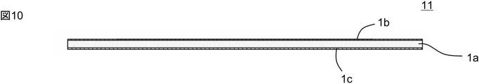
本発明の一実施形態の基材シート11は、図10に示すように、上述の基材層1と同様の構成を有することができる。すなわち、基材シート11は、クッション層1aとその上に設けられた表面処理層1bを備え、表面処理層1bは、アクリル系樹脂を含むアクリル系樹脂組成物で形成され、アクリル系樹脂が光照射又は加熱により架橋されている。基材シート11は、バリア層1cを備えてもよい。基材層1、クッション層1a、表面処理層1b、及びバリア層1cの説明は、「1-1.基材層1」と同様である。 3. Base Sheet As shown in FIG. 10, the
<実施例1>
実施例1では、クッション層1a上に表面処理層1bを形成し、表面処理層1b上に開口部2aを有する環状の粘着剤層2を形成することによって粘着シート10を製造した。 1. Production of
In Example 1, the pressure-
まず、150μm厚のエチレン-メタクリル酸共重合体の金属イオン架橋体(グンゼ社製 ファンクレアHMD)で構成されたクッション層1aを準備した。エチレン-メタクリル酸共重合体は、メタクリル酸単位の割合が15質量%、MFR(JIS K7210、125℃/10.0kg荷重)が5g/10min、融点(JIS K7121)が72℃であった。 Preparation of
エチルアクリレート80質量部、メチルメタクリレート12質量部、メタクリル酸2-ヒドロキシエチル5質量部、グリシジルメタクリレート3質量部を構成モノマーとしたアクリル系共重合体を重合し、このアクリル系共重合体100質量部に対して架橋剤(共栄社化学,ライトアクリレート1.9ND-A)を12質量部、光重合開始剤(BASF社製 オムニラット184)を1質量部添加することによって、表面処理剤を調製した。アクリル系共重合体は、架橋前のMwが60万、Tgが-7℃であり、架橋後のTgが32℃であった。 ・Formation of
水添ポリブタジエンジアクリレート(大阪有機社製、商品名BAC-45)54.4質量部、イソデシルアクリレート(大阪有機社製、商品名IDAA)13.6質量部、イソボニルアクリレート(大阪有機社製、商品名IBXA)32質量部、光重合開始剤としてα-アミノアルキルフェノン(BASF社製、商品名オムニラット379EG)7質量部、消泡剤としてビニルエーテルポリマー(共栄社化学社製、フローレンAC-903)3質量部、架橋剤として、イソシアネート(旭化成社製、商品名「TPA-100」)3質量部を加えて液状の組成物を準備した。この組成物を特定の形状に表面処理層1b上にスクリーン印刷し、UV照射後に40℃4日間のエージングを実施し、厚さ10μmの環状の粘着剤層2を形成した。 Formation of
クッション層1aに対してコロナ放電処理を行った後に表面処理層1bを形成した以外は、実施例1と同様の方法で粘着シート10を製造した。 <Example 2>
A pressure-
表面処理層1bを以下に示す方法で形成した以外は、実施例1と同様の方法で粘着シート10を製造した。 <Example 3>
A pressure-
エチルアクリレート50質量部、メチルメタクリレート42質量部、メタクリル酸2-ヒドロキシエチル5質量部、グリシジルメタクリレート3質量部を構成モノマーとしたアクリル系共重合体を重合し、このアクリル系共重合体100質量部に対してイソシアネート架橋剤(日本ポリウレタン株式会社:コロネートL-45E)を2質量部添加した表面処理剤を調製した。アクリル系共重合体は、架橋前のMwが60万、Tgが24℃であり、架橋後のTgが61℃であった。 ・Formation of
クッション層1aに対してコロナ放電処理を行った後に表面処理層1bを形成した以外は、実施例3と同様の方法で粘着シート10を製造した。 <Example 4>
A pressure-
表面処理層1bを形成せずに、クッション層1a上に粘着剤層2を形成した以外は、実施例1と同様の方法で粘着シート10を製造した。 <Comparative Example 1>
A pressure-
表面処理層1bを形成せずに、クッション層1a上に粘着剤層2を形成した以外は、実施例2と同様の方法で粘着シート10を製造した。 <Comparative Example 2>
A pressure-
表面処理層1bを以下に示す方法で形成した以外は、実施例2と同様の方法で粘着シート10を製造した。 <Comparative Example 3>
A pressure-
エチルアクリレート50質量部、メチルメタクリレート42質量部、メタクリル酸2-ヒドロキシエチル5質量部、グリシジルメタクリレート3質量部を構成モノマーとしたアクリル系共重合体を重合し、これを表面処理剤として、クッション層1a上にコーティングして、表面処理層1bを形成した。 - Formation of
粘着剤層2を以下に示す方法で形成した以外は、実施例2と同様の方法で粘着シート10を製造した。 <Comparative Example 4>
A pressure-
天然ゴム(ムーニー粘度75)100質量部、SIS(日本ゼオン社製、商品名「クインタック3460C」、放射状構造SIS、スチレン含有量25重量%)30質量部、無水マレイン酸変性C5,C9レジン(日本ゼオン社製、商品名「クイントンD-200」)40質量部をトルエンに溶解させた後、架橋剤として、芳香族イソシアネート(日本ポリウレタン社製、商品名「コロネートL」)3質量部を加えて溶液状のゴム系粘着剤組成物を準備した。この組成物をセパレーター上にコーティングし、加熱硬化することによって、厚さ10μmの粘着剤フィルムを得た。得られた粘着剤フィルムを開口部を有する形状に打ち抜き、表面処理層上に貼り合わせることによって、厚さ10μmの環状の粘着剤層2を形成した。 Formation of
上記作製した粘着シート10を用いて、以下の方法によって半導体ウエハ4の裏面研削を行った。 2. Grinding of Backside of Semiconductor Wafer Using the
まず、リングフレーム3に粘着シート10を貼り付けた。 <Frame attachment process>
First, the
次に、半導体ウエハ4の凸部5が設けられた面に粘着シート10を減圧チャンバ16内で半導体ウエハ4の外周部4aに貼り付けた。半導体ウエハ4としては、直径8インチ、厚さ725μmであり、高さ230μmのバンプ(突起電極)が、外周の3.0mm以外の領域に形成されているものを用いた。半導体ウエハ4が粘着剤層2に貼着されている貼付面の幅は、2.0mmとした。減圧チャンバ16内の圧力は、100Paであった。減圧チャンバ16内では基材層1を100℃に加温した。 <Wafer attachment process/heating process>
Next, the pressure-
次に、粘着シート10を半導体ウエハ4の外周に沿って切断して、リングフレーム3を粘着シート10から分離した。 <Cutting process>
Next, the
次に、支持フィルム7上に供給した硬化性樹脂8に粘着シート10を対面させた状態で、支持フィルム7の面内方向に粘着シート10を移動させることによって硬化性樹脂8を押し広げた。硬化性樹脂8は、1,2-水添ポリブタジエン末端ウレタン(メタ)アクリレート、イソボルニルアクリレート、ジエチルアクリルアミドで構成されるものを用いた。硬化性樹脂8の硬化前の粘度(E型粘度計を用いて、23℃及び50rpmの条件で測定)は470mPa・sであった。 <Resin curing step>
Next, the
次に、半導体ウエハ4の厚さが200μmになるまで、半導体ウエハ4の裏面研削を行った。裏面研削は、研磨機(株式会社ディスコ製バックグラインダーDFG-841)を用いて行った。 <Grinding process>
Next, the back surface of the
次に、半導体ウエハ4から粘着シート10を剥離した。 <Peeling process>
Next, the
製造した粘着シート10について、各評価を行った。その結果を表1に示す。 3. Evaluation Each evaluation was performed on the produced pressure-

<バンプ追従性>
以下に示す方法でバンプ追従性を評価した。 The details of the evaluation method are as follows.
<Bump followability>
Bump conformability was evaluated by the method shown below.
〇(優):追従率70%以上
×(不可):追従率70%未満 Bump followability was evaluated from the follow-up rate according to the following criteria.
○ (excellent): follow-up rate of 70% or more × (improper): follow-up rate of less than 70%
クッション層1a上に形成した表面処理層1bに碁盤目のクロスカット(1mm2のマス目を100個)を施した後、JIS Z 1522適合品のセロハン粘着テープ(ニチバン社製)を表面処理層1b上に貼り付け、指で強く押し付けた後、90°方向に剥離し、表面処理層1bの剥離の有無により評価を行った。
〇(優):剥がれ無し
×(不可):剥がれ有り <Adhesion between cushion layer and surface treatment layer>
After cross-cutting the
○ (excellent): no peeling × (improper): peeling
上記の「2.半導体ウエハの裏面研削」の剥離工程を行った後の、粘着シート10の粘着剤層2の剥がれを目視で観察した。
〇(優):剥がれなし
×(不可):半分以上もしくは全体が剥がれている <Adhesion between substrate layer and pressure-sensitive adhesive layer>
The peeling of the
〇 (excellent): No peeling × (improper): More than half or the whole peeled off
基材層とウエハの粘着力は、以下の方法で測定した。粘着シート10の中央付近の粘着剤層2が形成されていない部位(つまり、基材層が露出している部位)から、幅10mmで長さ100mmの試験片を切り出し、この試験片を用いて、JIS Z0237(2009)の粘着力の測定方法(方法1:テープ及びシートをステンレス試験板に対して180°に引きはがす試験方法)に準拠して測定した。具体的には、表面を洗浄した被着体(Siウエハ)に圧着装置(ローラの重量2kg)を用いて、試験片を圧着させた後、100℃のホットプレート上で1min加熱した。被着体に対して180°に試験片を引き剥がした際の粘着力を、温度23℃湿度50%の環境下において、万能型引張試験機(ORIENTEC社製 テンシロン 型番:RTG-1210)で、以下の条件で測定した測定結果を200mm幅での数値に換算した。
測定モード:引張り
引張り速度:300mm/min
チャック間距離:50mm
測定サンプル幅:10mm <Adhesive strength and peelability between substrate layer and wafer>
The adhesive strength between the substrate layer and the wafer was measured by the following method. A test piece having a width of 10 mm and a length of 100 mm is cut out from a portion near the center of the
Measurement mode: Tensile Tensile speed: 300mm/min
Distance between chucks: 50mm
Measurement sample width: 10 mm
〇(優):0.5~50N/200mm
×(不可):50N/200mm超 Based on the measurement results of the adhesive force obtained, the peelability between the substrate layer and the wafer was evaluated according to the following criteria.
○ (excellent): 0.5 to 50N/200mm
× (impossible): more than 50N/200mm
さらに上記の試験において、剥離後のシリコンウエハへの糊残りの有無を目視で確認し、以下の基準で評価した。
○(優):糊残り無し
×(不可):糊残り有り <Adhesive residue on wafer>
Furthermore, in the above test, the presence or absence of adhesive residue on the silicon wafer after peeling was visually confirmed and evaluated according to the following criteria.
○ (excellent): no adhesive residue × (improper): adhesive residue
離型処理の施されたポリエチレンテレフタレートフィルムの離型処理面に、各実施例・比較例で用いた表面処理剤を塗布し、100℃で1分間乾燥させることで25μmの表面処理層を得たのち、硬化反応を行ない、その後に表面処理層を幅3mm長さ7mmに型抜きしてサンプルとした。引張りモードにより、粘弾性測定装置(ティー・エイ・インスツルメント社製RSA-3)を用いて以下の条件で測定し180℃到達時点の貯蔵弾性率E'を得た。
周波数f=1Hz
温度30~180℃
昇温速度5℃/min
チャック間距離10mm <Storage elastic modulus E′ of the surface treatment layer at 180° C.>
The surface treatment agent used in each example and comparative example was applied to the release-treated surface of the release-treated polyethylene terephthalate film, and dried at 100° C. for 1 minute to obtain a 25 μm surface treatment layer. After that, a curing reaction was carried out, after which the surface treatment layer was punched into a sample having a width of 3 mm and a length of 7 mm. Using a viscoelasticity measuring device (RSA-3, manufactured by TA Instruments Co., Ltd.) in tensile mode, measurement was performed under the following conditions to obtain a storage modulus E' at the time of reaching 180°C.
frequency f = 1Hz
Temperature 30-180℃
Distance between chucks 10mm
Claims (8)
- 凸部を有する半導体ウエハの裏面研削用粘着シートであって、
基材層と、前記基材層上に設けられた粘着剤層と、を備え、
前記粘着剤層は、前記半導体ウエハの直径よりも小径の開口部を有し、前記半導体ウエハの凸部が前記開口部内に配置されるように前記半導体ウエハの外周部に貼着され、
前記半導体ウエハが前記粘着剤層に貼着された状態で前記凸部が前記基材層によって保護されるように構成され、
前記基材層は、クッション層とその上に設けられた表面処理層を備え、
前記粘着剤層は、前記表面処理層上に設けられ、
前記表面処理層は、アクリル系樹脂を含むアクリル系樹脂組成物で形成され、前記アクリル系樹脂が光照射又は加熱により架橋されており、
前記粘着剤層は、アクリル系樹脂を含むアクリル系樹脂組成物で形成されている、粘着シート。 A pressure-sensitive adhesive sheet for grinding the back surface of a semiconductor wafer having protrusions,
A substrate layer and an adhesive layer provided on the substrate layer,
The pressure-sensitive adhesive layer has an opening with a smaller diameter than the diameter of the semiconductor wafer, and is attached to the outer peripheral portion of the semiconductor wafer so that the convex portion of the semiconductor wafer is arranged in the opening,
The convex portion is protected by the base layer while the semiconductor wafer is attached to the adhesive layer,
The base material layer comprises a cushion layer and a surface treatment layer provided thereon,
The adhesive layer is provided on the surface treatment layer,
The surface treatment layer is formed of an acrylic resin composition containing an acrylic resin, and the acrylic resin is crosslinked by light irradiation or heating,
The pressure-sensitive adhesive sheet, wherein the pressure-sensitive adhesive layer is formed of an acrylic resin composition containing an acrylic resin. - 請求項1に記載の粘着シートであって、
前記表面処理層の180℃における貯蔵弾性率が1.0×10⁴Pa~1.0×10⁸Paである、粘着シート。 The pressure-sensitive adhesive sheet according to claim 1,
The pressure-sensitive adhesive sheet, wherein the surface treatment layer has a storage modulus of 1.0×10 4 Pa to 1.0×10 8 Pa at 180°C. - 請求項1又は請求項2に記載の粘着シートであって、
前記凸部は、前記基材層に埋入されることによって保護される、粘着シート。 The pressure-sensitive adhesive sheet according to claim 1 or claim 2,
The pressure-sensitive adhesive sheet, wherein the protrusions are protected by being embedded in the base material layer. - 請求項1又は請求項2に記載の粘着シートであって、
前記半導体ウエハは、減圧下で前記粘着剤層に貼着される、粘着シート。 The pressure-sensitive adhesive sheet according to claim 1 or claim 2,
The adhesive sheet, wherein the semiconductor wafer is attached to the adhesive layer under reduced pressure. - 請求項1又は請求項2に記載の粘着シートであって、
前記粘着シートから切り出した試験片の基材層を貼り合わせた前記半導体ウエハを100℃雰囲気下で1分間加熱し、常温に冷却した後の前記基材層と前記半導体ウエハとの23℃におけるJIS Z0237に準じて測定される粘着力が6N/200mm未満である、粘着シート。 The pressure-sensitive adhesive sheet according to claim 1 or claim 2,
The semiconductor wafer to which the base layer of the test piece cut out from the adhesive sheet is bonded is heated in an atmosphere of 100 ° C. for 1 minute, and after cooling to room temperature, the base layer and the semiconductor wafer are JIS at 23 ° C. A pressure-sensitive adhesive sheet having an adhesive strength of less than 6 N/200 mm as measured according to Z0237. - 請求項1又は請求項2に記載の粘着シートを用いた半導体ウエハの製造方法であって、
フレーム貼付工程と、ウエハ貼付工程と、加温工程と、切断工程と、樹脂硬化工程と、研削工程を備え、
前記フレーム貼付工程では、リングフレームに前記粘着シートを貼り付け、
前記ウエハ貼付工程では、前記半導体ウエハの凸部が設けられた面に前記粘着シートを減圧下で半導体ウエハの外周部に貼り付け、
前記加温工程では、前記基材層を加温し、
前記切断工程では、前記粘着シートを前記半導体ウエハの外周に沿って切断し、
前記樹脂硬化工程では、前記ウエハ貼付工程の後に前記基材層を硬化性樹脂に当接させ、その状態で前記硬化性樹脂を硬化させ、
前記研削工程では、前記半導体ウエハの裏面を研削する、半導体ウエハの製造方法。 A method for manufacturing a semiconductor wafer using the pressure-sensitive adhesive sheet according to claim 1 or 2,
A frame attachment process, a wafer attachment process, a heating process, a cutting process, a resin curing process, and a grinding process,
In the frame attaching step, the adhesive sheet is attached to the ring frame,
In the wafer attaching step, the adhesive sheet is attached to the surface of the semiconductor wafer provided with the convex portion under reduced pressure on the outer peripheral portion of the semiconductor wafer,
In the heating step, the base material layer is heated,
In the cutting step, the adhesive sheet is cut along the outer circumference of the semiconductor wafer,
In the resin curing step, the base material layer is brought into contact with a curable resin after the wafer attaching step, and the curable resin is cured in that state,
The method for manufacturing a semiconductor wafer, wherein in the grinding step, the back surface of the semiconductor wafer is ground. - 基材シートであって、
クッション層とその上に設けられた表面処理層を備え、
前記表面処理層は、アクリル系樹脂を含むアクリル系樹脂組成物で形成され、前記アクリル系樹脂が光照射又は加熱により架橋されている、基材シート。 A base sheet,
Equipped with a cushion layer and a surface treatment layer provided thereon,
The substrate sheet, wherein the surface treatment layer is formed of an acrylic resin composition containing an acrylic resin, and the acrylic resin is crosslinked by light irradiation or heating. - 請求項7に記載の基材シートであって、
前記表面処理層の180℃における貯蔵弾性率が1.0×10⁴Pa~1.0×10⁸Paである、基材シート。 The base sheet according to claim 7,
The base sheet, wherein the surface treatment layer has a storage elastic modulus at 180° C. of 1.0×10 4 Pa to 1.0×10 8 Pa.
Priority Applications (4)
| Application Number | Priority Date | Filing Date | Title |
|---|---|---|---|
| EP22811161.3A EP4333025A1 (en) | 2021-05-26 | 2022-05-11 | Adhesive sheet for rear surface grinding, semiconductor wafer manufacturing method, and base material sheet |
| KR1020237044784A KR20240013216A (en) | 2021-05-26 | 2022-05-11 | Manufacturing method of adhesive sheet for back grinding and semiconductor wafer, base sheet |
| CN202280037383.2A CN117378035A (en) | 2021-05-26 | 2022-05-11 | Adhesive sheet for back grinding, method for manufacturing semiconductor wafer, and base sheet |
| JP2023523404A JPWO2022249888A1 (en) | 2021-05-26 | 2022-05-11 |
Applications Claiming Priority (2)
| Application Number | Priority Date | Filing Date | Title |
|---|---|---|---|
| JP2021-088684 | 2021-05-26 | ||
| JP2021088684 | 2021-05-26 |
Publications (1)
| Publication Number | Publication Date |
|---|---|
| WO2022249888A1 true WO2022249888A1 (en) | 2022-12-01 |
Family
ID=84229872
Family Applications (1)
| Application Number | Title | Priority Date | Filing Date |
|---|---|---|---|
| PCT/JP2022/019981 WO2022249888A1 (en) | 2021-05-26 | 2022-05-11 | Adhesive sheet for rear surface grinding, semiconductor wafer manufacturing method, and base material sheet |
Country Status (6)
| Country | Link |
|---|---|
| EP (1) | EP4333025A1 (en) |
| JP (1) | JPWO2022249888A1 (en) |
| KR (1) | KR20240013216A (en) |
| CN (1) | CN117378035A (en) |
| TW (1) | TW202248390A (en) |
| WO (1) | WO2022249888A1 (en) |
Citations (6)
| Publication number | Priority date | Publication date | Assignee | Title |
|---|---|---|---|---|
| JP2010174067A (en) * | 2009-01-27 | 2010-08-12 | Furukawa Electric Co Ltd:The | Pressure-sensitive adhesive tape for surface protection |
| JP2012216619A (en) * | 2011-03-31 | 2012-11-08 | Lintec Corp | Surface protection sheet |
| JP2013211439A (en) * | 2012-03-30 | 2013-10-10 | Lintec Corp | Surface protection sheet |
| JP2018526826A (en) * | 2015-08-31 | 2018-09-13 | プリーヴァッサー, カール ハインツPRIEWASSER, Karl Heinz | Method for processing wafers and protective sheet for use in the method |
| JP2019140387A (en) | 2018-02-14 | 2019-08-22 | 株式会社ディスコ | Method of processing wafer |
| JP2020024976A (en) * | 2018-08-06 | 2020-02-13 | 株式会社ディスコ | Protective member forming device |
-
2022
- 2022-05-11 EP EP22811161.3A patent/EP4333025A1/en active Pending
- 2022-05-11 WO PCT/JP2022/019981 patent/WO2022249888A1/en active Application Filing
- 2022-05-11 KR KR1020237044784A patent/KR20240013216A/en unknown
- 2022-05-11 JP JP2023523404A patent/JPWO2022249888A1/ja active Pending
- 2022-05-11 CN CN202280037383.2A patent/CN117378035A/en active Pending
- 2022-05-23 TW TW111119040A patent/TW202248390A/en unknown
Patent Citations (6)
| Publication number | Priority date | Publication date | Assignee | Title |
|---|---|---|---|---|
| JP2010174067A (en) * | 2009-01-27 | 2010-08-12 | Furukawa Electric Co Ltd:The | Pressure-sensitive adhesive tape for surface protection |
| JP2012216619A (en) * | 2011-03-31 | 2012-11-08 | Lintec Corp | Surface protection sheet |
| JP2013211439A (en) * | 2012-03-30 | 2013-10-10 | Lintec Corp | Surface protection sheet |
| JP2018526826A (en) * | 2015-08-31 | 2018-09-13 | プリーヴァッサー, カール ハインツPRIEWASSER, Karl Heinz | Method for processing wafers and protective sheet for use in the method |
| JP2019140387A (en) | 2018-02-14 | 2019-08-22 | 株式会社ディスコ | Method of processing wafer |
| JP2020024976A (en) * | 2018-08-06 | 2020-02-13 | 株式会社ディスコ | Protective member forming device |
Also Published As
| Publication number | Publication date |
|---|---|
| JPWO2022249888A1 (en) | 2022-12-01 |
| TW202248390A (en) | 2022-12-16 |
| CN117378035A (en) | 2024-01-09 |
| EP4333025A1 (en) | 2024-03-06 |
| KR20240013216A (en) | 2024-01-30 |
Similar Documents
| Publication | Publication Date | Title |
|---|---|---|
| JP4369584B2 (en) | Adhesive sheet for semiconductor wafer holding protection | |
| JP6539336B2 (en) | Semiconductor processing sheet and method of manufacturing semiconductor device | |
| KR102544301B1 (en) | Laminate for resin film formation sheet | |
| JP2008143924A (en) | Repeelable adhesive composition, and adhesive tape or sheet | |
| JP6306362B2 (en) | Extensible sheet and laminated chip manufacturing method | |
| US20110008597A1 (en) | Surface protective sheet | |
| TW202016234A (en) | Semiconductor processing adhesive tape and method of manufacturing semiconductor device | |
| TW202020096A (en) | Adhesive tape for semiconductor processing and method for producing semiconductor device | |
| JP5414953B1 (en) | Dicing sheet and device chip manufacturing method | |
| JP6009188B2 (en) | Workpiece processing sheet base material and workpiece processing sheet | |
| WO2013141251A1 (en) | Film, sheet substrate for processing workpiece, and sheet for processing workpiece | |
| JPWO2019181730A1 (en) | Manufacturing method of adhesive tape and semiconductor device | |
| JP6207192B2 (en) | Adhesive sheet for semiconductor processing | |
| JP4947564B2 (en) | Adhesive sheet for semiconductor wafer processing | |
| JPWO2015141555A1 (en) | Dicing sheet and chip manufacturing method using the dicing sheet | |
| JPWO2015141555A6 (en) | Dicing sheet and chip manufacturing method using the dicing sheet | |
| JP5546232B2 (en) | Pressure sensitive adhesive tape for semiconductor surface protection | |
| WO2022249888A1 (en) | Adhesive sheet for rear surface grinding, semiconductor wafer manufacturing method, and base material sheet | |
| WO2022249889A1 (en) | Adhesive sheet for backgrinding, semiconductor wafer manufacturing method, and substrate sheet | |
| JP2017165880A (en) | Semiconductor processing sheet | |
| JP6343725B2 (en) | Base film for semiconductor processing sheet and semiconductor processing sheet | |
| WO2020175364A1 (en) | Back grinding adhesive sheet, and method for manufacturing semiconductor wafer | |
| JP6087122B2 (en) | Dicing sheet | |
| JP6190134B2 (en) | Dicing sheet base film, dicing sheet, dicing sheet base film manufacturing method, and chip-shaped member manufacturing method | |
| WO2022209119A1 (en) | Semiconductor processing adhesive tape, and method for manufacturing semiconductor device |
Legal Events
| Date | Code | Title | Description |
|---|---|---|---|
| 121 | Ep: the epo has been informed by wipo that ep was designated in this application |
Ref document number: 22811161 Country of ref document: EP Kind code of ref document: A1 |
|
| WWE | Wipo information: entry into national phase |
Ref document number: 2023523404 Country of ref document: JP |
|
| WWE | Wipo information: entry into national phase |
Ref document number: 18559745 Country of ref document: US |
|
| WWE | Wipo information: entry into national phase |
Ref document number: 2022811161 Country of ref document: EP |
|
| ENP | Entry into the national phase |
Ref document number: 2022811161 Country of ref document: EP Effective date: 20231129 |
|
| ENP | Entry into the national phase |
Ref document number: 20237044784 Country of ref document: KR Kind code of ref document: A |
|
| WWE | Wipo information: entry into national phase |
Ref document number: 1020237044784 Country of ref document: KR |
|
| NENP | Non-entry into the national phase |
Ref country code: DE |