WO2022244601A1 - コイル部品 - Google Patents
コイル部品 Download PDFInfo
- Publication number
- WO2022244601A1 WO2022244601A1 PCT/JP2022/018739 JP2022018739W WO2022244601A1 WO 2022244601 A1 WO2022244601 A1 WO 2022244601A1 JP 2022018739 W JP2022018739 W JP 2022018739W WO 2022244601 A1 WO2022244601 A1 WO 2022244601A1
- Authority
- WO
- WIPO (PCT)
- Prior art keywords
- coil
- conductor
- external electrode
- laminate
- coil component
- Prior art date
- Legal status (The legal status is an assumption and is not a legal conclusion. Google has not performed a legal analysis and makes no representation as to the accuracy of the status listed.)
- Ceased
Links
Images




Classifications
-
- G—PHYSICS
- G06—COMPUTING OR CALCULATING; COUNTING
- G06K—GRAPHICAL DATA READING; PRESENTATION OF DATA; RECORD CARRIERS; HANDLING RECORD CARRIERS
- G06K19/00—Record carriers for use with machines and with at least a part designed to carry digital markings
- G06K19/06—Record carriers for use with machines and with at least a part designed to carry digital markings characterised by the kind of the digital marking, e.g. shape, nature, code
- G06K19/067—Record carriers with conductive marks, printed circuits or semiconductor circuit elements, e.g. credit or identity cards also with resonating or responding marks without active components
- G06K19/07—Record carriers with conductive marks, printed circuits or semiconductor circuit elements, e.g. credit or identity cards also with resonating or responding marks without active components with integrated circuit chips
- G06K19/077—Constructional details, e.g. mounting of circuits in the carrier
- G06K19/07749—Constructional details, e.g. mounting of circuits in the carrier the record carrier being capable of non-contact communication, e.g. constructional details of the antenna of a non-contact smart card
- G06K19/07773—Antenna details
- G06K19/07777—Antenna details the antenna being of the inductive type
- G06K19/07784—Antenna details the antenna being of the inductive type the inductive antenna consisting of a plurality of coils stacked on top of one another
-
- G—PHYSICS
- G06—COMPUTING OR CALCULATING; COUNTING
- G06K—GRAPHICAL DATA READING; PRESENTATION OF DATA; RECORD CARRIERS; HANDLING RECORD CARRIERS
- G06K19/00—Record carriers for use with machines and with at least a part designed to carry digital markings
- G06K19/06—Record carriers for use with machines and with at least a part designed to carry digital markings characterised by the kind of the digital marking, e.g. shape, nature, code
- G06K19/067—Record carriers with conductive marks, printed circuits or semiconductor circuit elements, e.g. credit or identity cards also with resonating or responding marks without active components
- G06K19/07—Record carriers with conductive marks, printed circuits or semiconductor circuit elements, e.g. credit or identity cards also with resonating or responding marks without active components with integrated circuit chips
- G06K19/077—Constructional details, e.g. mounting of circuits in the carrier
- G06K19/0772—Physical layout of the record carrier
- G06K19/07722—Physical layout of the record carrier the record carrier being multilayered, e.g. laminated sheets
-
- G—PHYSICS
- G06—COMPUTING OR CALCULATING; COUNTING
- G06K—GRAPHICAL DATA READING; PRESENTATION OF DATA; RECORD CARRIERS; HANDLING RECORD CARRIERS
- G06K19/00—Record carriers for use with machines and with at least a part designed to carry digital markings
- G06K19/06—Record carriers for use with machines and with at least a part designed to carry digital markings characterised by the kind of the digital marking, e.g. shape, nature, code
- G06K19/067—Record carriers with conductive marks, printed circuits or semiconductor circuit elements, e.g. credit or identity cards also with resonating or responding marks without active components
- G06K19/07—Record carriers with conductive marks, printed circuits or semiconductor circuit elements, e.g. credit or identity cards also with resonating or responding marks without active components with integrated circuit chips
- G06K19/077—Constructional details, e.g. mounting of circuits in the carrier
- G06K19/07749—Constructional details, e.g. mounting of circuits in the carrier the record carrier being capable of non-contact communication, e.g. constructional details of the antenna of a non-contact smart card
- G06K19/07773—Antenna details
- G06K19/07777—Antenna details the antenna being of the inductive type
- G06K19/07779—Antenna details the antenna being of the inductive type the inductive antenna being a coil
- G06K19/07781—Antenna details the antenna being of the inductive type the inductive antenna being a coil the coil being fabricated in a winding process
-
- H—ELECTRICITY
- H01—ELECTRIC ELEMENTS
- H01F—MAGNETS; INDUCTANCES; TRANSFORMERS; SELECTION OF MATERIALS FOR THEIR MAGNETIC PROPERTIES
- H01F17/00—Fixed inductances of the signal type
-
- H—ELECTRICITY
- H01—ELECTRIC ELEMENTS
- H01F—MAGNETS; INDUCTANCES; TRANSFORMERS; SELECTION OF MATERIALS FOR THEIR MAGNETIC PROPERTIES
- H01F17/00—Fixed inductances of the signal type
- H01F17/0006—Printed inductances
- H01F17/0013—Printed inductances with stacked layers
-
- H—ELECTRICITY
- H03—ELECTRONIC CIRCUITRY
- H03H—IMPEDANCE NETWORKS, e.g. RESONANT CIRCUITS; RESONATORS
- H03H11/00—Networks using active elements
- H03H11/02—Multiple-port networks
- H03H11/28—Impedance matching networks
-
- H—ELECTRICITY
- H03—ELECTRONIC CIRCUITRY
- H03H—IMPEDANCE NETWORKS, e.g. RESONANT CIRCUITS; RESONATORS
- H03H7/00—Multiple-port networks comprising only passive electrical elements as network components
- H03H7/38—Impedance-matching networks
Definitions
- the present disclosure relates to coil components.
- a coil component including a coil such as a divider circuit When a coil component including a coil such as a divider circuit is realized with a multilayer electronic component, depending on the arrangement of the coil, capacitor, etc. formed inside the multilayer electronic component, parasitic capacitance may occur between the coil, capacitor, etc. and the electrodes. . A coil component with parasitic capacitance may not be able to obtain the required characteristics.
- an object of the present disclosure is to provide a coil component capable of obtaining required characteristics.
- a coil component is a coil component including a plurality of coils in a rectangular parallelepiped laminate.
- the coil component includes an external electrode at least partially formed on a side surface of the laminate, a first coil conductor whose winding axis is in the lamination direction of the laminate, and does not overlap the first coil conductor when viewed from the lamination direction.
- a second coil conductor formed at a position and having a winding axis in the stacking direction.
- the first coil conductor includes a plurality of conductor patterns laminated with an insulating layer interposed therebetween, and a connection conductor for electrically connecting the plurality of conductor patterns.
- the first coil conductor When the first region and the second region are divided by a bisector along the direction, the first coil conductor is positioned in the first region, and the minimum distance between the connection conductor and the external electrode is provided when viewed from the stacking direction.
- the connecting straight line crosses the opening area of the first coil conductor.
- the straight line connecting the connection conductor and the external electrode with the minimum distance crosses the opening region of the first coil conductor. can be separated from each other, the parasitic capacitance generated between the first coil conductor and the external electrode can be suppressed, and the characteristics required for the coil component can be obtained.
- FIG. 1 is a perspective view of a coil component according to an embodiment
- FIG. 1 is a plan view of a coil component according to an embodiment
- FIG. 4 is an equivalent circuit diagram of the coil component according to the embodiment
- FIG. FIG. 4 is a plan view for explaining a first coil conductor of a coil component for comparison
- FIG. 4 is an equivalent circuit diagram of a coil component for comparison
- 1 is a first exploded plan view showing the configuration of a coil component according to an embodiment
- FIG. FIG. 4 is a second exploded plan view showing the configuration of the coil component according to the embodiment
- FIG. 11 is a third exploded plan view showing the configuration of the coil component according to the embodiment
- FIG. 1 is a perspective view of a coil component according to an embodiment.
- FIG. 2 is a plan view of the coil component according to the embodiment.
- FIG. 3 is an equivalent circuit diagram of the coil component according to the embodiment. 1 and 2, the short side direction of the coil component 1 is the X direction, the long side direction is the Y direction, and the height direction is the Z direction. Also, the stacking direction of the substrates is the Z direction, and the direction of the arrow indicates the upper layer direction.
- the coil component 1 is, for example, a divider circuit in which a first coil conductor that does not constitute a transformer and a second coil conductor that constitutes a transformer are arranged adjacent to each other.
- a divider circuit is used as the configuration of the coil component 1, but the coil component is not limited to the divider circuit as long as it includes a plurality of coils in a rectangular parallelepiped laminate. Coil components can be applied.
- the coil component 1 includes a capacitor Cp1 and a coil Lp1 (first coil conductor) forming an LC resonator, and coils L1 to L3 (second coil conductors) forming a transformer section. , and capacitors CL1 and CL2.
- the coil component 1 has a transformer section connected to the rear stage of the LC resonator connected to the input terminal IN.
- the transformer section has an output terminal OUT1 connected to the capacitor CL1 and an output terminal OUT2 connected to the capacitor CL2. have.
- the coil component 1 is composed of a laminated body 3 in which a plurality of substrates on which wires for coils and capacitors are formed are laminated.
- the laminate 3 may be manufactured by, for example, a method of forming an electrode pattern using a photomask using a photosensitive conductive paste and a photosensitive insulating paste. Alternatively, for example, it may be manufactured by a method of laminating ceramic green sheets using a step of forming an electrode pattern by screen printing or a step of making holes in an insulating layer with a laser and filling via electrodes.
- the laminate 3 has a pair of main surfaces facing each other and side surfaces connecting the main surfaces.
- a plurality of conductor patterns 10 of the capacitor Cp1 and the coil Lp1 that form the LC resonator, a plurality of conductor patterns 20 of the coils L1 to L3 that form the transformer section, and a plurality of the capacitor CL1 are formed on the main surface of the laminate 3.
- a conductor pattern 30 is formed and stacked in the Z direction. Note that the capacitor CL2 is laminated on the coil Lp1 as described later, but is not shown in FIGS. 1 and 2.
- first external electrode 41 forming an input terminal IN
- second external electrode 42 forming a GND terminal
- third external electrode 43 forming an output terminal OUT1
- third external electrode 43 forming an output terminal OUT2.
- 4 external electrodes 44 are formed respectively. It should be noted that the first to fourth external electrodes 41 to 44 need not be formed at the four corners of the laminate 3, and may be formed around the periphery of the laminate 3. FIG. Also, the number of external electrodes formed on the outer periphery of the laminate 3 is not limited to four, and may be any number.
- the coil Lp1 is formed in the vicinity of the first external electrode 41 and the fourth external electrode 44, and the winding axis is in the stacking direction.
- a capacitor Cp1 is formed in a lower layer portion of the plurality of conductor patterns 10, and a coil Lp1 is formed in an upper layer portion thereof.
- Via conductors 51 and 52 connection conductors are provided to electrically connect between the plurality of conductor patterns 10 forming the coil Lp1.
- the via conductors 51 and 52 are arranged in the first external electrode 41 and the fourth external electrode 41 among the sides of the coil Lp1 parallel to the lateral direction (X direction) of the laminate 3 when viewed from the lamination direction. It is provided not on the side of the electrode 44 but on the side of the conductor pattern 20 . That is, via conductors 51 and 52 are provided at positions separated from first external electrode 41 and fourth external electrode 44 .
- FIG. 4 is a plan view for explaining the first coil conductor of the coil component for comparison.
- FIG. 5 is an equivalent circuit diagram of a coil component for comparison.
- via conductors 51 and 52 are provided on the side of the first external electrode 41 and the fourth external electrode 44 side.
- Coil component 1A has the same configuration as coil component 1 shown in FIG. 1 except for the positions where via conductors 51 and 52 are provided.
- the coil Lp1 of the LC resonator is arranged adjacent to the first external electrode 41 and the fourth external electrode 44, and the via conductors 51 and 52 of the coil Lp1 are arranged. are arranged at positions closest to the first external electrode 41 and the fourth external electrode 44 .
- the via conductors 51 and 52 are provided on the side of the first external electrode 41 and the fourth external electrode 44, a parasitic capacitance Cs1 is formed between the via conductor 51 and the first external electrode 41 as shown in FIG. is formed, and a parasitic capacitance Cs2 is formed between the via conductor 52 and the fourth external electrode 44 .
- the coil component 1A Due to the parasitic capacitances Cs1 and Cs2 generated between the via conductors 51 and 52 and the first external electrode 41 and the fourth external electrode 44, the coil component 1A provides isolation between the output terminal OUT1 and the output terminal OUT2. characteristics deteriorate.
- the via conductors 51 and 52 are provided at positions separated from the first external electrode 41 and the fourth external electrode 44 so that the via conductors 51 and 52 and the first external electrode 41 and the fourth external electrodes 44 are suppressed to ensure the required isolation characteristics.
- the coil Lp1 is shown in FIG. is located in the first region A.
- the via conductors 51 and 52 is located far from the coil Lp1. provided to the conductor of the side coil Lp1.
- the positions at which the via conductors 51 and 52 are spaced apart from the first external electrode 41 and the fourth external electrode 44 are the positions of the via conductors 51 and 52 and the first external electrode 41 and the fourth external electrode 44 when viewed from the stacking direction. It is sufficient that the straight lines I1 and I2 connecting between and at the minimum distance cross the opening region O of the coil Lp1.
- the conductor of the coil Lp1 on the side closer to the first external electrode 41 and the fourth external electrode 44 and the conductor of the coil Lp1 on the far side may be defined as follows. As shown in FIG. 2, the coil Lp1 has a side closer to the first external electrode 41 and the fourth external electrode 44 when the laminate 3 is divided into two equal parts in the longitudinal direction (Y direction) as viewed from the lamination direction. The side far from the first conductor 10A and the first external electrode 41 and the fourth external electrode 44 is defined as a second conductor 10B.
- both via conductors are not limited to being provided in the second conductor 10B. At least one of the via conductors 51 and 52 should be provided in the second conductor. Thereby, at least one of the parasitic capacitances Cs1 and Cs2 can be suppressed.
- the Q value of the coil deteriorates when via conductors are provided on the inside, since magnetic flux flows inside the coil.
- the coil Lp1 that does not constitute a transformer and the coils L1 to L3 that constitute the transformer included in the coil component 1 even if the Q value of the coil Lp1 that does not constitute a transformer deteriorates, the pass characteristic of the LC resonator does not change. have no effect. Therefore, by providing the via conductors 51 and 52 of the coil Lp1 whose Q value does not need to be considered inside the coil, it is possible to secure a larger area for the coil to be arranged in the laminate 3 . This is particularly effective for the coil component 1 in which the coil Lp1 and the coils L1 to L3 are arranged in the laminate 3 so as not to overlap each other.
- FIG. 6 is a first exploded plan view showing the configuration of the coil component according to the embodiment.
- FIG. 7 is a second exploded plan view showing the configuration of the coil component according to the embodiment.
- FIG. 8 is a third exploded plan view showing the configuration of the coil component according to the embodiment.
- the coil component 1 is formed by stacking ceramic green sheets shown in the first exploded plan view, the second exploded plan view, and the third exploded plan view in order from the bottom.
- conductive paste (Ni paste) is applied to ceramic green sheets 3a to 3l, which are substrates, for each of the conductor patterns of coils and capacitors and the electrode patterns of external electrodes. formed by
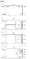
- Electrode patterns 41a to 44a of first to fourth external electrodes 41 to 44 are formed on the ceramic green sheet 3a, as shown in FIG. 6(a).
- electrode patterns 41b to 44b of first to fourth external electrodes 41 to 44 are formed on the ceramic green sheet 3b. Further, the ceramic green sheet 3b is formed with a conductor pattern 10b forming one electrode of the capacitor Cp1 on the right side in the drawing. The conductor pattern 10b has wiring for electrical connection with the electrode pattern 42b.
- Electrode patterns 41c to 44c of the first external electrode 41 to the fourth external electrode 44 are formed on the ceramic green sheet 3c, as shown in FIG. 6(c). Further, the ceramic green sheet 3c is formed with a conductor pattern 10c forming the other electrode of the capacitor Cp1 on the right side in the figure. Conductive pattern 10c is electrically connected to electrode pattern 41c.
- Electrode patterns 41d to 44d of the first external electrode 41 to the fourth external electrode 44 are formed on the ceramic green sheet 3d, as shown in FIG. 6(d). Further, the ceramic green sheet 3d is formed with a conductor pattern 10d forming a part of the coil Lp1 on the right side in the figure. The conductor pattern 10 d is electrically connected to the electrode pattern 41 d at one end and electrically connected to the connection portion 52 d connected to the via conductor 52 at the other end.
- Electrode patterns 41e to 44e of the first external electrode 41 to the fourth external electrode 44 are formed on the ceramic green sheet 3e, as shown in FIG. 7(e). Further, the ceramic green sheet 3e is formed with a conductor pattern 10e forming a part of the coil Lp1 on the right side in the drawing. Conductive pattern 10 e has one end electrically connected to connecting portion 51 e connected to via conductor 51 , and the other end electrically connected to connecting portion 52 e connected to via conductor 52 .
- Electrode patterns 41f to 44f of the first external electrode 41 to the fourth external electrode 44 are formed on the ceramic green sheet 3f, as shown in FIG. 7(f). Further, the ceramic green sheet 3f is formed with a conductor pattern 10f forming a part of the coil Lp1 on the right side in the figure. Conductive pattern 10 f has one end electrically connected to connecting portion 51 f connected to via conductor 51 , and the other end electrically connected to connecting portion 52 f connected to via conductor 52 .
- Electrode patterns 41g to 44g of the first external electrode 41 to the fourth external electrode 44 are formed on the ceramic green sheet 3g, as shown in FIG. 7(g). Further, the ceramic green sheet 3g is formed with a conductor pattern 10g forming a part of the coil Lp1 on the right side in the figure. Conductive pattern 10 g has one end electrically connected to connecting portion 51 g connected to via conductor 51 , and the other end electrically connected to connecting portion 52 g connected to via conductor 52 . A conductor pattern 20g forming part of the coil L2 of the transformer section is formed in the center of the drawing on the ceramic green sheet 3g.
- One end of the conductor pattern 20g is electrically connected to the electrode pattern 42g, and is electrically connected to the connection portion 53g that is connected to the via conductor.
- the region S1 in which the coil Lp1 is provided is narrower than the region S2 in which the coil L2 of the transformer section is provided.
- Electrode patterns 41h to 44h of the first external electrode 41 to the fourth external electrode 44 are formed on the ceramic green sheet 3h, as shown in FIG. 7(h). Further, the ceramic green sheet 3h is formed with a conductor pattern 10h forming a part of the coil Lp1 on the right side in the drawing. Conductive pattern 10 h has one end electrically connected to connecting portion 51 h connected to via conductor 51 , and the other end electrically connected to connecting portion 52 h connected to via conductor 52 . A conductor pattern 20h forming a part of the coil L2 of the transformer section is formed in the center of the drawing on the ceramic green sheet 3h.
- One end of the conductor pattern 20h is electrically connected to the electrode pattern 43h, and is electrically connected to the connection portion 53h that is connected to the via conductor.
- the conductor pattern 20g and the conductor pattern 20h are electrically connected by a via conductor provided between the connecting portion 53g and the connecting portion 53h to form a coil L2.
- electrode patterns 41i to 44i of the first external electrode 41 to the fourth external electrode 44 are formed on the ceramic green sheet 3i.
- the ceramic green sheet 3i is formed with a conductor pattern 10i forming a part of the coil Lp1 on the right side in the figure.
- Conductive pattern 10i has one end electrically connected to connection portion 51i connected to via conductor 51 and the other end electrically connected to connection portion 52i connected to via conductor 52 .
- a conductor pattern 20i forming part of the coil L1 of the transformer section is formed on the ceramic green sheet 3i in the center of the drawing.
- One end of the conductor pattern 20i is electrically connected to the electrode pattern 42i and is electrically connected to the connection portion 54i that is connected to the via conductor.
- Electrode patterns 41j to 44j of the first external electrode 41 to the fourth external electrode 44 are formed on the ceramic green sheet 3j, as shown in FIG. 8(j). Furthermore, a conductor pattern 10j forming one electrode of the capacitor CL2 is formed on the ceramic green sheet 3j on the right side in the drawing. A conductor pattern 30j forming one electrode of the capacitor CL1 is formed on the ceramic green sheet 3j on the left side in the figure. Furthermore, the ceramic green sheet 3j has a conductor pattern 20j forming a part of the coil L1 of the transformer section in the center of the figure. Conductive pattern 20j is electrically connected at one end to conductive pattern 10j and conductive pattern 30j, and is also electrically connected to connection portion 54j connected to a via conductor. The conductor pattern 20i and the conductor pattern 20j are electrically connected by a via conductor provided between the connecting portion 54i and the connecting portion 54j to form a coil L1.
- electrode patterns 41k to 44k of first to fourth external electrodes 41 to 44 are formed on the ceramic green sheet 3k.
- the ceramic green sheet 3k is formed with a conductor pattern 10k forming the other electrode of the capacitor CL2 on the right side in the drawing.
- the conductor pattern 10k is electrically connected to the electrode pattern 44k.
- a conductor pattern 30k forming the other electrode of the capacitor CL1 is formed on the ceramic green sheet 3k on the left side in the drawing.
- the conductor pattern 30k is electrically connected to the electrode pattern 43k.
- the ceramic green sheet 3k is formed with a conductor pattern 20k forming a part of the coil L3 of the transformer section in the center of the drawing.
- Conductive pattern 20k is electrically connected at one end to electrode pattern 42k and electrically connected to connection portion 55k that is connected to the via conductor.
- electrode patterns 41l to 44l of the first external electrode 41 to the fourth external electrode 44 are formed on the ceramic green sheet 3l.
- the ceramic green sheet 3l has a conductor pattern 20l forming a part of the coil L3 of the transformer section in the center of the drawing.
- One end of the conductor pattern 20l is electrically connected to the electrode pattern 44l, and is electrically connected to the connection portion 55l that is connected to the via conductor.
- the conductor pattern 20k and the conductor pattern 20l are electrically connected by a via conductor provided between the connecting portion 55k and the connecting portion 55l to form a coil L3.
- Coils L1 to L3 constitute a transformer in which a plurality of coils are stacked in the stacking direction.
- the first external electrodes 41 are configured by electrically connecting electrode patterns 41a to 41l formed on the ceramic green sheets 3a to 3l, respectively.
- the second external electrode 42 and the electrode patterns 42a to 42l formed on the ceramic green sheets 3a to 3l are electrically connected to each other.
- the third external electrodes 43 are configured by electrically connecting electrode patterns 43a to 43l formed on the ceramic green sheets 3a to 3l, respectively.
- the fourth external electrode 44 is configured by electrically connecting electrode patterns 44a to 44l formed on the ceramic green sheets 3a to 3l, respectively.
- each of the plurality of ceramic green sheets 3a to 3l shown in FIG. do.
- an unfired laminate 3 (ceramic body) is formed.
- the laminated body 3 thus formed is fired, and copper electrodes are baked on the outside of the fired laminated body 3 so as to be electrically connected to each of the first to fourth external electrodes 41 to 44 .
- the coil component 1 includes a plurality of coils in the rectangular parallelepiped laminate 3 .
- the coil component 1 includes first to fourth external electrodes 41 to 44 at least partially formed on the side surfaces of the laminate 3, a coil Lp1 whose winding axis is in the lamination direction of the laminate 3, and Coils L1 to L3 are formed at positions not overlapping with the coil Lp1 when viewed, and the winding axes thereof are in the stacking direction.
- Coil Lp1 includes a plurality of conductor patterns 10d-10i stacked with insulating layers interposed therebetween, and via conductors 51 and 52 for electrically connecting the plurality of conductor patterns 10d-10i.
- the coil Lp1 is positioned in the first region A when the bisector D divides the longitudinal direction of the laminate 3 into the first region A and the second region B as viewed from the stacking direction.
- straight lines I1 and I2 connecting via conductors 51 and 52 and first external electrode 41 and fourth external electrode 44 at minimum distances cross opening region O of coil Lp1.
- straight lines I1 and I2 connecting the via conductors 51 and 52 and the first external electrode 41 and the fourth external electrode 44 at the minimum distance when viewed from the stacking direction are the coils. Since it traverses the opening region O of Lp1, the via conductors 51 and 52 can be separated from the first external electrode 41 and the fourth external electrode 44, and the coil Lp1, the first external electrode 41 and the fourth external electrode 44 can be separated from each other. It is possible to suppress the parasitic capacitance generated between and obtain the characteristics required for the coil component 1 (for example, the isolation characteristics between the output terminal OUT1 and the output terminal OUT2).
- the side closer to the first external electrode 41 and the fourth external electrode 44 is defined as the first conductor 10A, the side farther from the first external electrode 41 and the fourth external electrode 44 is defined as the second conductor 10B.
- One via conductor is preferably provided in the second conductor 10B.
- At least one of the via conductors 51 and 52 is preferably provided on a side of the coil Lp1 parallel to the short direction of the laminate 3 when viewed from the stacking direction. Thereby, the parasitic capacitance generated between the coil Lp1 and the first external electrode 41 and the fourth external electrode 44 can be suppressed.
- the via conductors 51 and 52 are preferably provided inside the coil Lp1. As a result, more areas can be secured for the coil Lp1 and the coils L1 to L3 arranged in the laminate 3. FIG.
- the area S1 where the coil Lp1 is provided is preferably narrower than the area S2 where the coils L1 to L3 are provided. As a result, a large area can be secured for the transformer portion arranged in the laminate 3 .
- the coils L1 to L3 constitute a transformer in which a plurality of coils are stacked in the stacking direction.
- a divider circuit can be configured in which the coil Lp1 that does not constitute a transformer and the coils L1 to L3 that constitute a transformer are arranged adjacent to each other.
- the plurality of external electrodes are preferably first external electrodes 41 to fourth external electrodes 44 formed at the four corners of the laminate 3 .
- the plurality of external electrodes provided at the four corners of the laminate 3 can be electrically connected to the outside.
- the transformer section is configured by stacking the three coils L1 to L3 in the stacking direction, but it may be configured by stacking two or more coils in the stacking direction.
- the coil component 1 described so far has been described as being composed of a laminate 3 (ceramic element body) of a plurality of laminated ceramic layers, any dielectric multilayer structure may be used.
Landscapes
- Engineering & Computer Science (AREA)
- Microelectronics & Electronic Packaging (AREA)
- Computer Hardware Design (AREA)
- Physics & Mathematics (AREA)
- General Physics & Mathematics (AREA)
- Theoretical Computer Science (AREA)
- Computer Networks & Wireless Communication (AREA)
- Power Engineering (AREA)
- Coils Or Transformers For Communication (AREA)
Priority Applications (3)
| Application Number | Priority Date | Filing Date | Title |
|---|---|---|---|
| CN202280034579.6A CN117413328A (zh) | 2021-05-18 | 2022-04-25 | 线圈部件 |
| JP2023522586A JPWO2022244601A1 (https=) | 2021-05-18 | 2022-04-25 | |
| US18/382,612 US12288119B2 (en) | 2021-05-18 | 2023-10-23 | Coil component |
Applications Claiming Priority (2)
| Application Number | Priority Date | Filing Date | Title |
|---|---|---|---|
| JP2021083940 | 2021-05-18 | ||
| JP2021-083940 | 2021-05-18 |
Related Child Applications (1)
| Application Number | Title | Priority Date | Filing Date |
|---|---|---|---|
| US18/382,612 Continuation US12288119B2 (en) | 2021-05-18 | 2023-10-23 | Coil component |
Publications (1)
| Publication Number | Publication Date |
|---|---|
| WO2022244601A1 true WO2022244601A1 (ja) | 2022-11-24 |
Family
ID=84141401
Family Applications (1)
| Application Number | Title | Priority Date | Filing Date |
|---|---|---|---|
| PCT/JP2022/018739 Ceased WO2022244601A1 (ja) | 2021-05-18 | 2022-04-25 | コイル部品 |
Country Status (4)
| Country | Link |
|---|---|
| US (1) | US12288119B2 (https=) |
| JP (1) | JPWO2022244601A1 (https=) |
| CN (1) | CN117413328A (https=) |
| WO (1) | WO2022244601A1 (https=) |
Citations (3)
| Publication number | Priority date | Publication date | Assignee | Title |
|---|---|---|---|---|
| JPH04355902A (ja) * | 1990-07-24 | 1992-12-09 | Tdk Corp | 高周波回路 |
| JP2015164289A (ja) * | 2014-01-29 | 2015-09-10 | パナソニックIpマネジメント株式会社 | 共鳴結合器、伝送装置、スイッチングシステム、および、方向性結合器 |
| WO2018198604A1 (ja) * | 2017-04-26 | 2018-11-01 | 株式会社村田製作所 | 積層バラン |
Family Cites Families (13)
| Publication number | Priority date | Publication date | Assignee | Title |
|---|---|---|---|---|
| EP0523241B1 (en) | 1991-02-05 | 1997-07-23 | TDK Corporation | Dielectric filter |
| JPH10126191A (ja) * | 1996-10-14 | 1998-05-15 | Mitsubishi Materials Corp | 固体電子部品 |
| JPH10200357A (ja) | 1996-12-31 | 1998-07-31 | Taiyo Yuden Co Ltd | 積層型lc複合部品及びその特性調整方法 |
| JP4678563B2 (ja) * | 1999-05-25 | 2011-04-27 | 日立金属株式会社 | 積層型コモンモードチョークコイル |
| JP3228271B2 (ja) * | 1999-06-24 | 2001-11-12 | 株式会社村田製作所 | チョークコイル |
| JP2009295819A (ja) * | 2008-06-05 | 2009-12-17 | Murata Mfg Co Ltd | 電子部品 |
| JP6024418B2 (ja) * | 2012-11-28 | 2016-11-16 | Tdk株式会社 | コモンモードフィルタ |
| JP6421464B2 (ja) * | 2014-06-02 | 2018-11-14 | Tdk株式会社 | 積層コイル部品 |
| US9831837B2 (en) | 2014-11-05 | 2017-11-28 | Qualcomm Incorporated | Dynamic power divider circuits and methods |
| JP6432531B2 (ja) * | 2015-03-27 | 2018-12-05 | 株式会社村田製作所 | 積層コイル部品 |
| JP6332114B2 (ja) * | 2015-04-06 | 2018-05-30 | 株式会社村田製作所 | 積層コイル部品、その製造方法およびスクリーン印刷版 |
| JP6551169B2 (ja) * | 2015-11-05 | 2019-07-31 | Tdk株式会社 | 積層ローパスフィルタ |
| JP7238622B2 (ja) * | 2019-06-21 | 2023-03-14 | Tdk株式会社 | 積層コイル部品 |
-
2022
- 2022-04-25 JP JP2023522586A patent/JPWO2022244601A1/ja active Pending
- 2022-04-25 CN CN202280034579.6A patent/CN117413328A/zh active Pending
- 2022-04-25 WO PCT/JP2022/018739 patent/WO2022244601A1/ja not_active Ceased
-
2023
- 2023-10-23 US US18/382,612 patent/US12288119B2/en active Active
Patent Citations (3)
| Publication number | Priority date | Publication date | Assignee | Title |
|---|---|---|---|---|
| JPH04355902A (ja) * | 1990-07-24 | 1992-12-09 | Tdk Corp | 高周波回路 |
| JP2015164289A (ja) * | 2014-01-29 | 2015-09-10 | パナソニックIpマネジメント株式会社 | 共鳴結合器、伝送装置、スイッチングシステム、および、方向性結合器 |
| WO2018198604A1 (ja) * | 2017-04-26 | 2018-11-01 | 株式会社村田製作所 | 積層バラン |
Also Published As
| Publication number | Publication date |
|---|---|
| JPWO2022244601A1 (https=) | 2022-11-24 |
| US20240046063A1 (en) | 2024-02-08 |
| US12288119B2 (en) | 2025-04-29 |
| CN117413328A (zh) | 2024-01-16 |
Similar Documents
| Publication | Publication Date | Title |
|---|---|---|
| JP7322934B2 (ja) | コイル部品および、これを含むフィルタ回路 | |
| TWI442624B (zh) | Laminated bandpass filter | |
| JP6801826B2 (ja) | フィルタ素子 | |
| US8947189B2 (en) | Multilayer chip inductor and production method for same | |
| JP6508145B2 (ja) | 電子部品 | |
| JP2002057543A (ja) | 積層型lc部品 | |
| JP2019050460A (ja) | 積層型電子部品 | |
| JPH0775208B2 (ja) | インダクター及びインダクターを含む複合部品並びにそれらの製造方法 | |
| JP6597541B2 (ja) | 電子部品 | |
| JP2011004324A (ja) | 積層複合フィルタ | |
| WO2018212273A1 (ja) | 積層型電子部品 | |
| WO2018070105A1 (ja) | 積層型lcフィルタアレイ | |
| WO2022244601A1 (ja) | コイル部品 | |
| JP2003109818A (ja) | 積層インダクタ | |
| CN109659112B (zh) | 绕组用芯体及其制造方法、带绕组的电子部件 | |
| JP2023042194A (ja) | 積層型電子部品 | |
| JP2001110638A (ja) | 積層電子部品 | |
| JP2003168945A (ja) | Lcノイズフィルタおよびその製造方法 | |
| TWI849500B (zh) | 積層型電子零件 | |
| TWI849501B (zh) | 積層型電子零件 | |
| JPH0661054A (ja) | Lc複合部品 | |
| WO2023157666A1 (ja) | インダクタ、およびインダクタを備えた電子部品 | |
| WO2023157577A1 (ja) | 電子部品 | |
| JPH1116737A (ja) | インダクタアレイ | |
| JP2006246124A (ja) | 積層型ノイズフィルタ |
Legal Events
| Date | Code | Title | Description |
|---|---|---|---|
| 121 | Ep: the epo has been informed by wipo that ep was designated in this application |
Ref document number: 22804515 Country of ref document: EP Kind code of ref document: A1 |
|
| WWE | Wipo information: entry into national phase |
Ref document number: 2023522586 Country of ref document: JP |
|
| WWE | Wipo information: entry into national phase |
Ref document number: 202280034579.6 Country of ref document: CN |
|
| NENP | Non-entry into the national phase |
Ref country code: DE |
|
| 122 | Ep: pct application non-entry in european phase |
Ref document number: 22804515 Country of ref document: EP Kind code of ref document: A1 |