WO2022239696A1 - 半導体装置 - Google Patents
半導体装置 Download PDFInfo
- Publication number
- WO2022239696A1 WO2022239696A1 PCT/JP2022/019513 JP2022019513W WO2022239696A1 WO 2022239696 A1 WO2022239696 A1 WO 2022239696A1 JP 2022019513 W JP2022019513 W JP 2022019513W WO 2022239696 A1 WO2022239696 A1 WO 2022239696A1
- Authority
- WO
- WIPO (PCT)
- Prior art keywords
- electrode
- semiconductor device
- thickness direction
- joint
- bonding layer
- Prior art date
- Legal status (The legal status is an assumption and is not a legal conclusion. Google has not performed a legal analysis and makes no representation as to the accuracy of the status listed.)
- Ceased
Links
Images















Classifications
-
- H—ELECTRICITY
- H10—SEMICONDUCTOR DEVICES; ELECTRIC SOLID-STATE DEVICES NOT OTHERWISE PROVIDED FOR
- H10W—GENERIC PACKAGES, INTERCONNECTIONS, CONNECTORS OR OTHER CONSTRUCTIONAL DETAILS OF DEVICES COVERED BY CLASS H10
- H10W74/00—Encapsulations, e.g. protective coatings
- H10W74/10—Encapsulations, e.g. protective coatings characterised by their shape or disposition
- H10W74/111—Encapsulations, e.g. protective coatings characterised by their shape or disposition the semiconductor body being completely enclosed
- H10W74/127—Encapsulations, e.g. protective coatings characterised by their shape or disposition the semiconductor body being completely enclosed characterised by arrangements for sealing or adhesion
-
- H—ELECTRICITY
- H10—SEMICONDUCTOR DEVICES; ELECTRIC SOLID-STATE DEVICES NOT OTHERWISE PROVIDED FOR
- H10W—GENERIC PACKAGES, INTERCONNECTIONS, CONNECTORS OR OTHER CONSTRUCTIONAL DETAILS OF DEVICES COVERED BY CLASS H10
- H10W74/00—Encapsulations, e.g. protective coatings
- H10W74/10—Encapsulations, e.g. protective coatings characterised by their shape or disposition
- H10W74/111—Encapsulations, e.g. protective coatings characterised by their shape or disposition the semiconductor body being completely enclosed
-
- H—ELECTRICITY
- H10—SEMICONDUCTOR DEVICES; ELECTRIC SOLID-STATE DEVICES NOT OTHERWISE PROVIDED FOR
- H10W—GENERIC PACKAGES, INTERCONNECTIONS, CONNECTORS OR OTHER CONSTRUCTIONAL DETAILS OF DEVICES COVERED BY CLASS H10
- H10W70/00—Package substrates; Interposers; Redistribution layers [RDL]
- H10W70/40—Leadframes
- H10W70/411—Chip-supporting parts, e.g. die pads
-
- H—ELECTRICITY
- H10—SEMICONDUCTOR DEVICES; ELECTRIC SOLID-STATE DEVICES NOT OTHERWISE PROVIDED FOR
- H10W—GENERIC PACKAGES, INTERCONNECTIONS, CONNECTORS OR OTHER CONSTRUCTIONAL DETAILS OF DEVICES COVERED BY CLASS H10
- H10W70/00—Package substrates; Interposers; Redistribution layers [RDL]
- H10W70/40—Leadframes
- H10W70/464—Additional interconnections in combination with leadframes
- H10W70/466—Tape carriers or flat leads
-
- H—ELECTRICITY
- H10—SEMICONDUCTOR DEVICES; ELECTRIC SOLID-STATE DEVICES NOT OTHERWISE PROVIDED FOR
- H10W—GENERIC PACKAGES, INTERCONNECTIONS, CONNECTORS OR OTHER CONSTRUCTIONAL DETAILS OF DEVICES COVERED BY CLASS H10
- H10W70/00—Package substrates; Interposers; Redistribution layers [RDL]
- H10W70/40—Leadframes
- H10W70/481—Leadframes for devices being provided for in groups H10D8/00 - H10D48/00
-
- H—ELECTRICITY
- H10—SEMICONDUCTOR DEVICES; ELECTRIC SOLID-STATE DEVICES NOT OTHERWISE PROVIDED FOR
- H10W—GENERIC PACKAGES, INTERCONNECTIONS, CONNECTORS OR OTHER CONSTRUCTIONAL DETAILS OF DEVICES COVERED BY CLASS H10
- H10W72/00—Interconnections or connectors in packages
-
- H—ELECTRICITY
- H10—SEMICONDUCTOR DEVICES; ELECTRIC SOLID-STATE DEVICES NOT OTHERWISE PROVIDED FOR
- H10W—GENERIC PACKAGES, INTERCONNECTIONS, CONNECTORS OR OTHER CONSTRUCTIONAL DETAILS OF DEVICES COVERED BY CLASS H10
- H10W72/00—Interconnections or connectors in packages
- H10W72/30—Die-attach connectors
-
- H—ELECTRICITY
- H10—SEMICONDUCTOR DEVICES; ELECTRIC SOLID-STATE DEVICES NOT OTHERWISE PROVIDED FOR
- H10W—GENERIC PACKAGES, INTERCONNECTIONS, CONNECTORS OR OTHER CONSTRUCTIONAL DETAILS OF DEVICES COVERED BY CLASS H10
- H10W90/00—Package configurations
-
- H—ELECTRICITY
- H10—SEMICONDUCTOR DEVICES; ELECTRIC SOLID-STATE DEVICES NOT OTHERWISE PROVIDED FOR
- H10W—GENERIC PACKAGES, INTERCONNECTIONS, CONNECTORS OR OTHER CONSTRUCTIONAL DETAILS OF DEVICES COVERED BY CLASS H10
- H10W90/00—Package configurations
- H10W90/811—Multiple chips on leadframes
-
- H—ELECTRICITY
- H10—SEMICONDUCTOR DEVICES; ELECTRIC SOLID-STATE DEVICES NOT OTHERWISE PROVIDED FOR
- H10W—GENERIC PACKAGES, INTERCONNECTIONS, CONNECTORS OR OTHER CONSTRUCTIONAL DETAILS OF DEVICES COVERED BY CLASS H10
- H10W72/00—Interconnections or connectors in packages
- H10W72/071—Connecting or disconnecting
- H10W72/076—Connecting or disconnecting of strap connectors
- H10W72/07651—Connecting or disconnecting of strap connectors characterised by changes in properties of the strap connectors during connecting
- H10W72/07653—Connecting or disconnecting of strap connectors characterised by changes in properties of the strap connectors during connecting changes in shapes
-
- H—ELECTRICITY
- H10—SEMICONDUCTOR DEVICES; ELECTRIC SOLID-STATE DEVICES NOT OTHERWISE PROVIDED FOR
- H10W—GENERIC PACKAGES, INTERCONNECTIONS, CONNECTORS OR OTHER CONSTRUCTIONAL DETAILS OF DEVICES COVERED BY CLASS H10
- H10W72/00—Interconnections or connectors in packages
- H10W72/60—Strap connectors, e.g. thick copper clips for grounding of power devices
- H10W72/631—Shapes of strap connectors
-
- H—ELECTRICITY
- H10—SEMICONDUCTOR DEVICES; ELECTRIC SOLID-STATE DEVICES NOT OTHERWISE PROVIDED FOR
- H10W—GENERIC PACKAGES, INTERCONNECTIONS, CONNECTORS OR OTHER CONSTRUCTIONAL DETAILS OF DEVICES COVERED BY CLASS H10
- H10W72/00—Interconnections or connectors in packages
- H10W72/60—Strap connectors, e.g. thick copper clips for grounding of power devices
- H10W72/631—Shapes of strap connectors
- H10W72/637—Multiple strap connectors having different shapes
-
- H—ELECTRICITY
- H10—SEMICONDUCTOR DEVICES; ELECTRIC SOLID-STATE DEVICES NOT OTHERWISE PROVIDED FOR
- H10W—GENERIC PACKAGES, INTERCONNECTIONS, CONNECTORS OR OTHER CONSTRUCTIONAL DETAILS OF DEVICES COVERED BY CLASS H10
- H10W72/00—Interconnections or connectors in packages
- H10W72/60—Strap connectors, e.g. thick copper clips for grounding of power devices
- H10W72/681—Auxiliary members, e.g. flow barriers
- H10W72/685—Alignment aids, e.g. alignment marks
-
- H—ELECTRICITY
- H10—SEMICONDUCTOR DEVICES; ELECTRIC SOLID-STATE DEVICES NOT OTHERWISE PROVIDED FOR
- H10W—GENERIC PACKAGES, INTERCONNECTIONS, CONNECTORS OR OTHER CONSTRUCTIONAL DETAILS OF DEVICES COVERED BY CLASS H10
- H10W72/00—Interconnections or connectors in packages
- H10W72/851—Dispositions of multiple connectors or interconnections
- H10W72/853—On the same surface
- H10W72/871—Bond wires and strap connectors
-
- H—ELECTRICITY
- H10—SEMICONDUCTOR DEVICES; ELECTRIC SOLID-STATE DEVICES NOT OTHERWISE PROVIDED FOR
- H10W—GENERIC PACKAGES, INTERCONNECTIONS, CONNECTORS OR OTHER CONSTRUCTIONAL DETAILS OF DEVICES COVERED BY CLASS H10
- H10W72/00—Interconnections or connectors in packages
- H10W72/851—Dispositions of multiple connectors or interconnections
- H10W72/874—On different surfaces
- H10W72/884—Die-attach connectors and bond wires
-
- H—ELECTRICITY
- H10—SEMICONDUCTOR DEVICES; ELECTRIC SOLID-STATE DEVICES NOT OTHERWISE PROVIDED FOR
- H10W—GENERIC PACKAGES, INTERCONNECTIONS, CONNECTORS OR OTHER CONSTRUCTIONAL DETAILS OF DEVICES COVERED BY CLASS H10
- H10W72/00—Interconnections or connectors in packages
- H10W72/851—Dispositions of multiple connectors or interconnections
- H10W72/874—On different surfaces
- H10W72/886—Die-attach connectors and strap connectors
-
- H—ELECTRICITY
- H10—SEMICONDUCTOR DEVICES; ELECTRIC SOLID-STATE DEVICES NOT OTHERWISE PROVIDED FOR
- H10W—GENERIC PACKAGES, INTERCONNECTIONS, CONNECTORS OR OTHER CONSTRUCTIONAL DETAILS OF DEVICES COVERED BY CLASS H10
- H10W72/00—Interconnections or connectors in packages
- H10W72/90—Bond pads, in general
- H10W72/921—Structures or relative sizes of bond pads
- H10W72/926—Multiple bond pads having different sizes
-
- H—ELECTRICITY
- H10—SEMICONDUCTOR DEVICES; ELECTRIC SOLID-STATE DEVICES NOT OTHERWISE PROVIDED FOR
- H10W—GENERIC PACKAGES, INTERCONNECTIONS, CONNECTORS OR OTHER CONSTRUCTIONAL DETAILS OF DEVICES COVERED BY CLASS H10
- H10W74/00—Encapsulations, e.g. protective coatings
-
- H—ELECTRICITY
- H10—SEMICONDUCTOR DEVICES; ELECTRIC SOLID-STATE DEVICES NOT OTHERWISE PROVIDED FOR
- H10W—GENERIC PACKAGES, INTERCONNECTIONS, CONNECTORS OR OTHER CONSTRUCTIONAL DETAILS OF DEVICES COVERED BY CLASS H10
- H10W90/00—Package configurations
- H10W90/701—Package configurations characterised by the relative positions of pads or connectors relative to package parts
- H10W90/731—Package configurations characterised by the relative positions of pads or connectors relative to package parts of die-attach connectors
- H10W90/736—Package configurations characterised by the relative positions of pads or connectors relative to package parts of die-attach connectors between a chip and a stacked lead frame, conducting package substrate or heat sink
-
- H—ELECTRICITY
- H10—SEMICONDUCTOR DEVICES; ELECTRIC SOLID-STATE DEVICES NOT OTHERWISE PROVIDED FOR
- H10W—GENERIC PACKAGES, INTERCONNECTIONS, CONNECTORS OR OTHER CONSTRUCTIONAL DETAILS OF DEVICES COVERED BY CLASS H10
- H10W90/00—Package configurations
- H10W90/701—Package configurations characterised by the relative positions of pads or connectors relative to package parts
- H10W90/751—Package configurations characterised by the relative positions of pads or connectors relative to package parts of bond wires
- H10W90/756—Package configurations characterised by the relative positions of pads or connectors relative to package parts of bond wires between a chip and a stacked lead frame, conducting package substrate or heat sink
-
- H—ELECTRICITY
- H10—SEMICONDUCTOR DEVICES; ELECTRIC SOLID-STATE DEVICES NOT OTHERWISE PROVIDED FOR
- H10W—GENERIC PACKAGES, INTERCONNECTIONS, CONNECTORS OR OTHER CONSTRUCTIONAL DETAILS OF DEVICES COVERED BY CLASS H10
- H10W90/00—Package configurations
- H10W90/701—Package configurations characterised by the relative positions of pads or connectors relative to package parts
- H10W90/761—Package configurations characterised by the relative positions of pads or connectors relative to package parts of strap connectors
- H10W90/763—Package configurations characterised by the relative positions of pads or connectors relative to package parts of strap connectors between laterally-adjacent chips
-
- H—ELECTRICITY
- H10—SEMICONDUCTOR DEVICES; ELECTRIC SOLID-STATE DEVICES NOT OTHERWISE PROVIDED FOR
- H10W—GENERIC PACKAGES, INTERCONNECTIONS, CONNECTORS OR OTHER CONSTRUCTIONAL DETAILS OF DEVICES COVERED BY CLASS H10
- H10W90/00—Package configurations
- H10W90/701—Package configurations characterised by the relative positions of pads or connectors relative to package parts
- H10W90/761—Package configurations characterised by the relative positions of pads or connectors relative to package parts of strap connectors
- H10W90/766—Package configurations characterised by the relative positions of pads or connectors relative to package parts of strap connectors between a chip and a stacked lead frame, conducting package substrate or heat sink
Definitions
- the present disclosure relates to semiconductor devices.
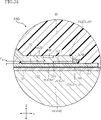
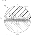
- FIG. 34 is a cross-sectional view taken along line XXXIV-XXXIV of FIG. 33.
- FIG. 35 is a cross-sectional view taken along line XXXV-XXXV of FIG. 33.
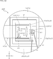
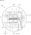
- FIG. FIG. 36 is a partially enlarged plan view of a modification of the semiconductor device shown in FIG. 33, which is transparent through the sealing resin.
- FIG. 37 is a partially enlarged plan view of the semiconductor device according to the seventh embodiment of the present disclosure, enlarging the first element and its surroundings and seeing through the sealing resin. 38 is a cross-sectional view taken along line XXXVIII-XXXVIII of FIG. 37.
- the support member 10 is composed of the same lead frame together with the plurality of terminal leads 13 .
- the lead frame is copper (Cu) or a copper alloy.
- the composition of the support member 10 and the plurality of terminal leads 13 includes copper (ie, these members contain copper).
- the support member 10 has electrical conductivity.
- the support member 10 includes a first die pad 10A and a second die pad 10B spaced apart from each other in the first direction x, as shown in FIGS.
- Support member 10 has a main surface 101 and a back surface 102 .
- the main surface 101 faces the thickness direction z.
- Main surface 101 is covered with sealing resin 50 .
- a semiconductor element 21 is mounted on the main surface 101 . Therefore, the back surface 102 faces the side opposite to the side where the semiconductor element 21 is located in the thickness direction z.
- the rear surface 102 is exposed from the sealing resin 50 .
- Back surface 102 is plated with tin (Sn), for example.
- the sealing resin 50 is applied to the semiconductor element 21, the conductive member 30, and a portion of the support member 10 (a portion of each of the first die pad 10A and the second die pad 10B). ) and Furthermore, the sealing resin 50 partially covers each of the plurality of terminal leads 13 .
- the sealing resin 50 has electrical insulation.
- Sealing resin 50 is made of a material containing, for example, black epoxy resin.
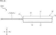
- the dimension L1 of the sealing resin 50 in the first direction x is longer than the dimension L2 of the sealing resin 50 in the second direction y.
- the sealing resin 50 has a top surface 51 , a bottom surface 52 , a pair of first side surfaces 53 , a second side surface 54 , a third side surface 55 , a plurality of recesses 56 and grooves 57 .
- the plurality of terminal leads 13 are positioned on one side of the support member 10 in the second direction y, as shown in FIG. A plurality of terminal leads 13 are electrically connected to the semiconductor element 21 . A plurality of terminal leads 13 are arranged along the first direction x.
- the plurality of terminal leads 13 includes a first input terminal 14 , an output terminal 15 , a second input terminal 16 , a first gate terminal 171 , a second gate terminal 172 , a first sense terminal 181 and a second sense terminal 182 .
- the output terminal 15 includes a portion extending along the second direction y and is connected to the second die pad 10B. Therefore, the output terminal 15 is electrically connected to the second electrode 212 of the second element 21B through the second die pad 10B.
- the AC power converted by the semiconductor element 21 is output from the output terminal 15 .
- the output terminal 15 has a covered portion 15A and an exposed portion 15B.
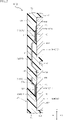
- the covering portion 15A is connected to the second die pad 10B and covered with the sealing resin 50. As shown in FIG. When viewed in the first direction x, the covering portion 15A is bent in the same manner as the covering portion 14A of the first input terminal 14 . As shown in FIGS.
- the conduction member 30 forms a conduction path in the semiconductor device A10 together with the support member 10 and the plurality of terminal leads 13.
- the composition of the conducting member 30 contains copper.
- Conductive member 30 is a metal clip.
- conductive member 30 includes a first conductive member 31 and a second conductive member 32, as shown in FIGS.
- the second joint portion 313 is joined to the first bearing surface 103 of the second die pad 10B.
- the second joint portion 313 extends in the second direction y. At least part of the second joint portion 313 is housed in a region defined by the first seat surface 103 and the first standing surface 104 of the second die pad 10B.
- the second joint portion 313 is connected to the body portion 311 .
- the second joint portion 313 is located on the opposite side of the first joint portion 312 with the body portion 311 interposed therebetween.
- the fourth joint portion 323 is joined to the second seating surface 16C of the second input terminal 16. As shown in FIG. The fourth joint portion 323 extends in the first direction x. At least part of the fourth joint portion 323 is accommodated in a region defined by the second seat surface 16C and the second upright surface 16D of the second input terminal 16. As shown in FIG. The fourth joint portion 323 is connected to the body portion 321 . The fourth joint portion 323 is located on the side opposite to the third joint portion 322 with the body portion 321 interposed therebetween.
- the semiconductor device A10 further includes a third bonding layer 35, as shown in FIGS. In FIG. 14, the third bonding layer 35 is indicated by a plurality of points.
- the third bonding layer 35 is interposed between the first electrode 211 of the second element 21B and the third bonding portion 322 .
- the third bonding layer 35 bonds the first electrode 211 of the second element 21B and the third bonding portion 322 .
- the third bonding layer 35 has conductivity.
- the third bonding layer 35 is solder.
- the thickness t of the third bonding portion 322 is 0.1 mm or more and twice the maximum thickness T max of the third bonding layer 35 or less.
- the maximum thickness T max of the third bonding layer 35 is greater than the thickness of the second element 21B.
- the semiconductor device A10 further includes a fourth bonding layer 36, as shown in FIGS.
- the fourth bonding layer 36 is interposed between the second seating surface 16 ⁇ /b>C of the second input terminal 16 and the fourth bonding portion 323 .
- the fourth joint layer 36 joins the covering portion 16A of the second input terminal 16 and the fourth joint portion 323 .
- the fourth bonding layer 36 has conductivity.
- the fourth bonding layer 36 is solder.
- the first restrictor 37A faces the first bonding layer 33 in the first direction x.
- the first restricting body 37A is in contact with the first bonding layer 33 and the end surface 312B of the first bonding portion 312 of the first conduction member 31 .
- the first restricting body 37A includes a first portion 371 and a second portion 372 that are separated from each other in the second direction y. A portion of the first bonding layer 33 is located between the first portion 371 and the second portion 372 .
- the second restrictor 37B faces the third bonding layer 35 in the first direction x.
- the second restrictor 37B is in contact with the third bonding layer 35 and the end surface 322B of the third bonding portion 322 of the second conduction member 32 .
- the second restrictor 37B includes a first portion 371 and a second portion 372 that are separated from each other in the second direction y. A portion of the third bonding layer 35 is located between the first portion 371 and the second portion 372 .
- the pair of detection wires 42 includes the second electrodes 212 of the first element 21A and the second element 21B, the covering portion 181A of the first detecting terminal 181, and the covering portion 182A of the second detecting terminal 182. and are joined separately.
- the first detection terminal 181 is electrically connected to the second electrode 212 of the first element 21A.
- the second detection terminal 182 is electrically connected to the second electrode 212 of the second element 21B.
- the composition of the pair of sensing wires 42 includes gold.
- the composition of the pair of detection wires 42 may contain copper or aluminum.
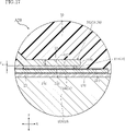
- the semiconductor device A10 includes a semiconductor element 21 (first element 21A) having a first electrode 211, a conduction member 30 (first conduction member 31) having a first joint portion 312 facing the semiconductor element 21, and a first electrode 211. 211 and a bonding layer (first bonding layer 33 ) interposed between the first bonding portion 312 .
- the semiconductor device A10 further includes a regulating body 37 (first regulating body 37A) joined to the first electrode 211 .
- the regulator 37 faces the first bonding layer 33 in a direction perpendicular to the thickness direction z.
- the first joint portion 312 of the conducting member 30 has an end face 312B facing the first direction x.
- the end surface 312B is in contact with the restrictor 37.
- the first bonding portion 312 is bonded to the first electrode 211 of the semiconductor element 21 via the first bonding layer 33 , the first bonding portion 312 is positioned in the first direction x to the gate electrode 213 of the semiconductor element 21 .
- the end face 312B comes into contact with the regulating body 37. Therefore, the end face 312B serves as means for bringing the first joint portion 312 into contact with the restricting body 37 more reliably.
- the regulating body 37 includes a first portion 371 and a second portion 372 positioned apart from each other in the second direction y. As a result, it is possible to reduce the volume of the regulation body 37 while suppressing the displacement of the conductive member 30 with respect to the first electrode 211 of the semiconductor element 21 . Furthermore, the regulator 37 contains a metal element. The metal element is aluminum. As a result, the regulating body 37 becomes a conductive path between the first electrode 211 of the semiconductor element 21 and the first joint portion 312 of the conductive member 30 . In addition, the liquid repellency of the melted first bonding layer 33 with respect to the regulator 37 is improved. Therefore, the regulating body 37 can more effectively block the melted first bonding layer 33 .
- the sealing resin 50 has a plurality of recesses 56 recessed from the third side surface 55 in the second direction y. With this configuration, any two terminal leads 13 among the plurality of terminal leads 13 (excluding the first gate terminal 171 and the first detection terminal 181 and the second gate terminal 172 and the second detection terminal 182). A longer creepage distance of the sealing resin 50 between is ensured. Thereby, the withstand voltage of the semiconductor device A10 can be improved.
- the sealing resin 50 has a groove portion 57 recessed from the bottom surface 52 and dividing the rear surface 102 of the first die pad 10A and the rear surface 102 of the second die pad 10B when viewed in the thickness direction z.
- This configuration ensures a longer creeping distance of the sealing resin 50 between the first die pad 10A and the second die pad 10B. This makes it possible to further improve the withstand voltage of the semiconductor device A10.
- thermal strain in the first direction x of the sealing resin 50 can be dispersed. As a result, concentration of thermal strain on the pair of first side surfaces 53 of the sealing resin 50 can be alleviated.
- FIGS. 16 and 18 are transparent through the sealing resin 50 for convenience of understanding.
- the position in FIG. 16 is the same as the position in FIG. 12 of the semiconductor device A10.
- the position in FIG. 18 is the same as the position in FIG. 14 of the semiconductor device A10.
- the semiconductor device A20 differs from the semiconductor device A10 in the configuration of the regulator 37.
- the first restricting body 37A is joined to the joint surface 312A of the first joint portion 312 of the first conducting member 31. As shown in FIGS. The first restrictor 37A is in contact with the first electrode 211 of the first element 21A. Therefore, like the first bonding layer 33, the first restricting body 37A is interposed between the first electrode 211 of the first element 21A and the bonding surface 312A. In the semiconductor device A20, the first restricting body 37A is formed by bonding a metal block to the bonding surface 312A by wire bonding.
- FIG. 20 is transparent through the sealing resin 50 for convenience of understanding.
- the position of FIG. 20 is the same as the position of FIG.
- the configuration of this modification includes not only the relationship between the first electrode 211 of the first element 21A and the first conductive member 31 shown below, but also the relationship between the first electrode 211 of the second element 21B shown in FIGS. , the relationship with the second conductive member 32 .
- the first electrode 211 of the first element 21A has an extension 211B.
- the extended portion 211B is located on the side opposite to the first joint portion 312 with the tip portion 314 interposed therebetween.
- the first bonding layers 33 are positioned on both sides of the first restrictor 37A in the first direction x.
- the first bonding layer 33 is in contact with the extended portion 211B of the first electrode 211 of the first element 21A and the distal end portion 314 of the first conductive member 31 .
- the second restricting body 37B is also sandwiched between the first electrode 211 of the second element 21B and the joint surface 322A of the third joint portion 322 of the second conductive member 32. As shown in FIG. With this configuration, the maximum thickness T max of the third bonding layer 35 can be made equal (or substantially equal) to the thickness of the second restrictor 37B. Therefore, it becomes easy to manage the maximum thickness T max of the third bonding layer 35 .
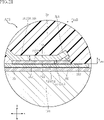
- the conduction member 30 of the semiconductor device A21 has a tip portion 314 connected to the first joint portion 312 .
- the distal end portion 314 is formed on the joint surface of the first joint portion 312 in a direction away from the first electrode 211 of the semiconductor element 21 in the thickness direction z as it becomes farther from the first joint portion 312 in the direction orthogonal to the thickness direction z. It is tilted with respect to 312A.
- the first electrode 211 when viewed in the thickness direction z, has an extended portion 211B located on the opposite side of the first joint portion 312 with the tip portion 314 interposed therebetween.
- the first bonding layer 33 is in contact with the extended portion 211B, and the first bonding layer 33 crawls up along the tip portion 314 . Thereby, a fillet having a relatively large volume is formed in the first bonding layer 33 . Therefore, it is possible to improve the bonding strength of the conductive member 30 to the first electrode 211 and allow a larger current to flow through the conductive member 30 .
- the inclination angle ⁇ of the tip portion 314 with respect to the joint surface 312A is preferably 30° or more and 60° or less. When the inclination angle ⁇ is set within this range, the formation of the fillet of the first bonding layer 33 is promoted and the concentration of thermal stress at the interface between the extension portion 211B and the first bonding layer 33 is reduced.
- the regulator 37 contains a metal element.
- the metal element is aluminum.
- the regulating body 37 becomes a conductive path between the first electrode 211 of the semiconductor element 21 and the first joint portion 312 of the conductive member 30 .
- the liquid repellency of the melted first bonding layer 33 with respect to the regulator 37 is improved.
- the reaction force that the regulation body 37 receives from the first bonding layer 33 is increased. Therefore, the effect of restraining the displacement of the conducting member 30 by the restricting body 37 is improved.
- the first joint portion 312 of the first conduction member 31 includes two regions that are separated from each other in the second direction y. As shown in FIG. 25, one of the two regions is bonded to the top electrode 221 of the first diode 22A via the first bonding layer 33. As shown in FIG. Thereby, the upper surface electrode 221 of the first diode 22A is electrically connected to the first electrode 211 of the first element 21A through the first conduction member 31. As shown in FIG.
- the regulator 37 of the semiconductor device A40 includes a third regulator 37C joined to the upper electrode 221 of the first diode 22A and a fourth regulator 37D joined to the upper electrode 221 of the second diode 22B.
- the semiconductor device A50 differs from the semiconductor device A10 in the configuration of the conductive member 30.
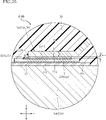
- the convex portion 38 protrudes in the thickness direction z from the joint surface 312A of the third joint portion 322 toward the first electrode 211 of the second element 21B.
- the convex portion 38 is in contact with the first electrode 211 of the second element 21B and the third bonding layer 35 .
- the dimension d of the convex portion 38 in the thickness direction z is smaller than the dimension h of the second restricting body 37B in the thickness direction z.
- the projection 38 has a circular shape when viewed in the thickness direction z.
- the projection 38 may have a polygonal shape such as a square shape when viewed in the thickness direction z.
- the convex portion 38 of the first conduction member 31 includes a first convex portion 381 and a second convex portion 382 that are positioned apart from each other in the first direction x.
- the shape and size of the first protrusion 381 and the second protrusion 382 are equal to each other.
- FIG. 32 is transparent through the sealing resin 50 for convenience of understanding.
- the position of FIG. 32 is the same as the position of FIG.
- the configuration of this modification can be applied not only to the first conduction member 31 described below, but also to the second conduction member 32 shown in FIGS.
- the convex portion 38 of the first conduction member 31 includes a first convex portion 381 and a second convex portion 382 that are positioned apart from each other in the second direction y.
- the first protrusion 381 and the second protrusion 382 extend in the first direction x. That is, the first protrusion 381 and the second protrusion 382 extend in a direction orthogonal to the thickness direction z and the direction in which the first protrusion 381 and the second protrusion 382 separate from each other.
- the dimension a in the first direction x is larger than the dimension b in the second direction y.
- the first protrusion 381 and the second protrusion 382 of the protrusion 38 are orthogonal to the thickness direction z and the direction in which the first protrusion 381 and the second protrusion 382 are separated from each other. extending in the direction
- the first bonding portion 312 of the conductive member 30 is bonded to the first electrode 211 of the semiconductor element 21 via the first bonding layer 33, the first bonding portion 312 moves in the first direction x and in the first direction. Rotational displacement around each of the two directions y can be suppressed.
- FIG. 33 is transparent through the sealing resin 50 for convenience of understanding.
- the position in FIG. 33 is the same as the position in FIG. 27 of the semiconductor device A50.
- the configuration of the present embodiment includes not only the relationship between the first electrode 211 of the first element 21A and the first conductive member 31 described below, but also the relationship between the first electrode 211 of the second element 21B and the relationship shown in FIGS. , the relationship with the second conductive member 32 .
- the first electrode 211 of the first element 21A includes two regions separated from each other in the first direction x.
- the first conducting member 31 has two first joints 312 spaced apart from each other in the first direction x.
- One side of the two first joint portions 312 in the second direction y is connected to the body portion 311 of the first conduction member 31 .
- the convex portion 38 protrudes in the thickness direction z from the joint surfaces 312A of the two first joint portions 312 toward the first electrode 211 of the first element 21A.
- the convex portion 38 is in contact with the first electrode 211 of the first element 21A and the first bonding layer 33 .
- the convex portion 38 includes a first convex portion 381 and a second convex portion 382 spaced apart from each other in the first direction x.
- the first convex portion 381 is provided on one first joint portion 312 of the two first joint portions 312 .
- the second convex portion 382 is provided on the other first joint portion 312 of the two first joint portions 312 . As shown in FIG.
- the semiconductor device A60 includes a semiconductor element 21 (first element 21A) having a first electrode 211, a conduction member 30 (first conduction member 31) having a first joint portion 312 facing the semiconductor element 21, and a first electrode 211. 211 and a bonding layer (first bonding layer 33 ) interposed between the first bonding portion 312 .
- the semiconductor device A50 further includes a regulating body 37 (first regulating body 37A) joined to the first electrode 211 .
- the regulator 37 faces the first bonding layer 33 in a direction perpendicular to the thickness direction z.
- the semiconductor device A60 can also suppress the displacement of the conductive member 30 with respect to the electrode (first electrode 211) of the semiconductor element 21.
- FIG. since the semiconductor device A60 has the same configuration as the semiconductor device A10, the semiconductor device A60 also exhibits the effects of the configuration.
- the conducting member 30 of the semiconductor device A60 has the projections 38 provided on the two first joints 312 .
- the convex portion 38 protrudes in the thickness direction z toward the first electrode 211 of the semiconductor element 21 .
- the protrusion 38 is in contact with the first electrode 211 . Therefore, since the semiconductor device A60 can also control the maximum thickness T max of the first bonding layer 33 shown in FIG. 34, it is possible to improve the durability of the semiconductor device A60 against temperature cycles and power cycles. . Furthermore, the generation of voids in the first bonding layer 33 can be suppressed.
- FIG. 37 is transparent through the sealing resin 50 for convenience of understanding.
- the position in FIG. 37 is the same as the position in FIG. 16 of the semiconductor device A20.
- the configuration of this embodiment is not limited to the relationship between the first conducting member 31 and the first restricting body 37A described below, but also the relationship between the second conducting member 32 and the second restricting body 37B shown in FIGS. can also be applied.
- the semiconductor device A70 differs from the semiconductor device A20 in the configuration of the conductive member 30 and the restrictor 37.
- the recessed portion 39 is recessed in the thickness direction z from the upper surface 312D of the first joint portion 312 toward the first electrode 211 of the first element 21A.
- the upper surface 312D faces the side opposite to the joint surface 312A of the first joint portion 312 in the thickness direction z and is connected to the end surface 312B of the first joint portion 312 .
- the shape of the recessed portion 39 approximates the shape of the convex portion 38 when viewed in the thickness direction z.
- the recessed portion 39 overlaps the convex portion 38 when viewed in the thickness direction z. In this case, the dimension d in the thickness direction z of the convex portion 38 is equal to or less than the thickness t of the first joint portion 312 .
- the conducting member 30 of the semiconductor device A70 has a convex portion 38 provided on the first joint portion 312 .
- the convex portion 38 protrudes in the thickness direction z toward the first electrode 211 of the semiconductor element 21 .
- the protrusion 38 is in contact with the first electrode 211 . Therefore, since the semiconductor device A70 can also control the maximum thickness T max of the first bonding layer 33 shown in FIG. 38, it is possible to improve the durability of the semiconductor device A70 against temperature cycles and power cycles. . Furthermore, the generation of voids in the first bonding layer 33 can be suppressed.
- the dimension d in the thickness direction z of the protrusion 38 shown in FIG. 38 is larger than the dimension h in the thickness direction z of the restricting body 37.
- FIGS. A semiconductor device A80 according to the eighth embodiment of the present disclosure will be described as shown in FIGS.
- elements identical or similar to those of the semiconductor device A10 described above are denoted by the same reference numerals, and overlapping descriptions are omitted.
- FIG. 39 is transparent through the sealing resin 50 for convenience of understanding.
- the position in FIG. 39 is the same as the position in FIG. 22 of the semiconductor device A30.
- the configuration of this embodiment can be applied not only to the first conducting member 31 described below, but also to the second conducting member 32 shown in FIG.
- the semiconductor device A80 differs from the semiconductor device A30 in the configuration of the conducting member 30.
- the first conducting member 31 has a convex portion 38 and an indented portion 39. As shown in FIG. The convex portion 38 and the recessed portion 39 are provided at the first joint portion 312 of the first conducting member 31 . The convex portion 38 and the recessed portion 39 can be formed by pressing the first joint portion 312 .
- the recessed portion 39 is recessed in the thickness direction z from the upper surface 312D of the first joint portion 312 toward the first electrode 211 of the first element 21A.
- the upper surface 312D faces the side opposite to the joint surface 312A of the first joint portion 312 in the thickness direction z and is connected to the end surface 312B of the first joint portion 312 .
- the shape of the recessed portion 39 approximates the shape of the convex portion 38 when viewed in the thickness direction z.
- the recessed portion 39 overlaps the convex portion 38 when viewed in the thickness direction z. In this case, the dimension d in the thickness direction z of the convex portion 38 is equal to or less than the thickness t of the first joint portion 312 .
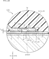
- the semiconductor device A80 includes a semiconductor element 21 (first element 21A) having a first electrode 211, a conduction member 30 (first conduction member 31) having a first joint portion 312 facing the semiconductor element 21, and a first electrode 211. 211 and a bonding layer (first bonding layer 33 ) interposed between the first bonding portion 312 .
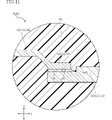
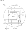
- the first electrode 211 has a first recess 211A recessed in a direction orthogonal to the thickness direction z.
- the first joint portion 312 has a second concave portion 312C that is concave in a direction orthogonal to the thickness direction z. When viewed in the thickness direction z, the second recess 312C overlaps the first recess 211A.
- the semiconductor device A80 can also allow the positional deviation of the conductive member 30 with respect to the electrode (first electrode 211) of the semiconductor element 21.
- FIG. since the semiconductor device A80 has the same configuration as the semiconductor device A10, the semiconductor device A80 also exhibits the effects of the configuration.
- the conductive member 30 of the semiconductor device A80 has a convex portion 38 provided on the first joint portion 312 .
- the convex portion 38 protrudes in the thickness direction z toward the first electrode 211 of the semiconductor element 21 .
- the protrusion 38 is in contact with the first electrode 211 . Therefore, since the semiconductor device A80 can also control the maximum thickness T max of the first bonding layer 33 shown in FIG. 40, it is possible to improve the durability of the semiconductor device A80 against temperature cycles and power cycles. . Furthermore, the generation of voids in the first bonding layer 33 can be suppressed.
- the conductive member has a tip portion connected to the first joint portion, The tip portion is inclined with respect to the joint surface in a direction away from the first electrode in the thickness direction as the distance from the first joint portion increases in a direction orthogonal to the thickness direction, 8.
- Appendix 9. The semiconductor device according to any one of appendices 1 to 8, wherein the regulator is in contact with the bonding layer.
- the semiconductor element has a gate electrode positioned on the same side as the first electrode in the thickness direction, 10.
- a semiconductor element having a first electrode; a conductive member having a first joint facing the first electrode; a bonding layer interposed between the first electrode and the first bonding portion; the first electrode has a first recess recessed in a direction perpendicular to the thickness direction of the semiconductor element, The first joint has a second recess recessed in a direction orthogonal to the thickness direction, The semiconductor device, wherein the second recess overlaps the first recess when viewed in the thickness direction.
- the semiconductor element has a gate electrode positioned on the same side as the first electrode in the thickness direction, 12.
- Appendix 13. further comprising a support member located on the opposite side of the semiconductor element from the first joint portion in the thickness direction; 13.
- Appendix 14. 14 The semiconductor device according to appendix 13, further comprising a sealing resin that covers the semiconductor element, the conduction member, and part of the support member.
- Appendix 15. further comprising a plurality of terminal leads electrically connected to the semiconductor element; 15.
- the semiconductor device according to appendix 14 wherein a part of each of the plurality of terminal leads is covered with the sealing resin.
- Appendix 16. The support member has conductivity, The semiconductor element has a second electrode facing the support member, The second electrode is joined to the support member, 16.
- the semiconductor device according to appendix 15, wherein one of the plurality of terminal leads is connected to the support member.
- Appendix 17. The conducting member has a main body portion to which the first joint portion is connected, and a second joint portion connected to the main body portion and positioned apart from the first joint portion, 17.
- the conducting member has a convex portion provided at the first joint portion and protruding in the thickness direction toward the first electrode; 18.
- Appendix 19 The conductive member has a recessed portion provided in the first joint portion and recessed in the thickness direction toward the first electrode, 19.
- the convex portion includes a first convex portion and a second convex portion positioned apart from each other in a direction perpendicular to the thickness direction, The first convex portion and the second convex portion extend in a direction orthogonal to the thickness direction and the direction in which the first convex portion and the second convex portion separate from each other. 21.
Landscapes
- Structures Or Materials For Encapsulating Or Coating Semiconductor Devices Or Solid State Devices (AREA)
- Lead Frames For Integrated Circuits (AREA)
Abstract
Description
付記1.
第1電極を有する半導体素子と、
前記第1電極に対向する第1接合部を有する導通部材と、
前記第1電極と前記第1接合部との間に介在する接合層と、
前記第1電極および前記第1接合部のいずれかに接合された規制体と、を備え、
前記半導体素子の厚さ方向に対して直交する方向において、前記規制体は、前記接合層に対向している、半導体装置。
付記2.
前記規制体は、金属元素を含む、付記1に記載の半導体装置。
付記3.
前記金属元素は、アルミニウムである、付記2に記載の半導体装置。
付記4.
前記規制体は、前記第1電極に接合されており、
前記第1接合部は、前記厚さ方向に対して直交する第1方向を向く端面を有し、
前記端面は、前記規制体に接触している、付記2または3に記載の半導体装置。
付記5.
前記規制体は、前記厚さ方向および前記第1方向に対して直交する第2方向において互いに離れて位置する第1部および第2部を含む、付記4に記載の半導体装置。
付記6.
前記接合層の一部が、前記第1部と前記第2部との間に位置する、付記5に記載の半導体装置。
付記7.
前記第1接合部は、前記第1電極に対向する接合面を有し、
前記規制体は、前記接合面に接合されており、
前記規制体は、前記第1電極に接している、付記2または3に記載の半導体装置。
付記8.
前記導通部材は、前記第1接合部につながる先端部を有し、
前記先端部は、前記厚さ方向に対して直交する方向において前記第1接合部から遠ざかるほど、前記厚さ方向において前記第1電極から遠ざかる向きに前記接合面に対して傾斜しており、
前記厚さ方向に視て、前記第1電極は、前記先端部を間に挟んで前記第1接合部とは反対側に位置する拡張部を有する、付記7に記載の半導体装置。
付記9.
前記規制体は、前記接合層に接している、付記1ないし8のいずれかに記載の半導体装置。
付記10.
前記半導体素子は、前記厚さ方向において前記第1電極と同じ側に位置するゲート電極を有し、
前記厚さ方向に視て、前記ゲート電極と前記第1接合部との間に前記第1電極の一部が位置する、付記1ないし9のいずれかに記載の半導体装置。
付記11.
第1電極を有する半導体素子と、
前記第1電極に対向する第1接合部を有する導通部材と、
前記第1電極と前記第1接合部との間に介在する接合層と、を備え、
前記第1電極は、前記半導体素子の厚さ方向に対して直交する方向に凹む第1凹部を有し、
前記第1接合部は、前記厚さ方向に対して直交する方向に凹む第2凹部を有し、
前記厚さ方向に視て、前記第2凹部は、前記第1凹部に重なっている、半導体装置。
付記12.
前記半導体素子は、前記厚さ方向において前記第1電極と同じ側に位置するゲート電極を有し、
前記厚さ方向に視て、前記ゲート電極は、前記第1凹部および前記第2凹部に重なっている、付記11に記載の半導体装置。
付記13.
前記厚さ方向において前記半導体素子に対して前記第1接合部とは反対側に位置する支持部材をさらに備え、
前記半導体素子は、前記支持部材に搭載されている、付記1ないし12のいずれかに記載の半導体装置。
付記14.
前記半導体素子および前記導通部材と、前記支持部材の一部と、を覆う封止樹脂をさらに備える、付記13に記載の半導体装置。
付記15.
前記半導体素子に導通する複数の端子リードをさらに備え、
前記複数の端子リードの各々の一部は、前記封止樹脂に覆われている、付記14に記載の半導体装置。
付記16.
前記支持部材は、導電性を有しており、
前記半導体素子は、前記支持部材に対向する第2電極を有し、
前記第2電極は、前記支持部材に接合されており、
前記複数の端子リードのいずれかが、前記支持部材につながっている、付記15に記載の半導体装置。
付記17.
前記導通部材は、前記第1接合部がつながる本体部と、前記本体部につながり、かつ前記第1接合部とは離れて位置する第2接合部を有し、
前記第2接合部は、前記複数の端子リードのいずれかに接合されている、付記15または16のいずれかに記載の半導体装置。
付記18.
前記導通部材は、前記第1接合部に設けられ、かつ前記第1電極に向けて前記厚さ方向に突出する凸部を有し、
前記凸部は、前記第1電極に接している、付記1ないし17のいずれかに記載の半導体装置。
付記19.
前記導通部材は、前記第1接合部に設けられ、かつ前記第1電極に向けて前記厚さ方向に凹む陥入部を有し、
前記厚さ方向に視て、前記陥入部は、前記凸部に重なっている、付記18に記載の半導体装置。
付記20.
前記凸部の前記厚さ方向の寸法は、前記第1接合部の厚さ以下である、付記19に記載の半導体装置。
付記21.
前記凸部は、前記厚さ方向に対して直交する方向に互いに離れて位置する第1凸部および第2凸部を含み、
前記第1凸部および前記第2凸部は、前記厚さ方向と、前記第1凸部および前記第2凸部が互いに離れる方向と、に対して直交する方向に延びている、付記18ないし20のいずれかに記載の半導体装置。
10:支持部材 10A:第1ダイパッド
10B:第2ダイパッド 101:主面
102:裏面 103:第1座面
104:第1起立面 13:端子リード
14:第1入力端子 14A:被覆部
14B:露出部 15:出力端子
15A:被覆部 15B:露出部
16:第2入力端子 16A:被覆部
16B:露出部 16C:第2座面
16D:第2起立面 171:第1ゲート端子
171A:被覆部 171B:露出部
172:第2ゲート端子 172A:被覆部
172B:露出部 181:第1検出端子
181A:被覆部 181B:露出部
182:第2検出端子 182A:被覆部
182B:露出部 21:半導体素子
21A:第1素子 21B:第2素子
211:第1電極 211A:第1凹部
211B:拡張部 212:第2電極
213:ゲート電極 22:保護素子
22A:第1ダイオード 22B:第2ダイオード
221:上面電極 222:下面電極
23:ダイボンディング層 31:第1導通部材
311:本体部 312:第1接合部
312A:接合面 312B:端面
312C:第2凹部 312D:上面
313:第2接合部 314:先端部
32:第2導通部材 321:本体部
322:第3接合部 322A:接合面
322B:端面 322C:第2凹部
322D:上面 323:第4接合部
33:第1接合層 34:第2接合層
35:第3接合層 36:第4接合層
37:規制体 37A:第1規制体
37B:第2規制体 37C:第3規制体
37D:第4規制体 371:第1部
372:第2部 38:凸部
381:第1凸部 382:第2凸部
39:陥入部 41:ゲートワイヤ
42:検出ワイヤ 50:封止樹脂
51:頂面 52:底面
53:第1側面 54:第2側面
55:第3側面 56:凹部
57:溝部 z:厚さ方向
x:第1方向 y:第2方向
Claims (21)
- 第1電極を有する半導体素子と、
前記第1電極に対向する第1接合部を有する導通部材と、
前記第1電極と前記第1接合部との間に介在する接合層と、
前記第1電極および前記第1接合部のいずれかに接合された規制体と、を備え、
前記半導体素子の厚さ方向に対して直交する方向において、前記規制体は、前記接合層に対向している、半導体装置。 - 前記規制体は、金属元素を含む、請求項1に記載の半導体装置。
- 前記金属元素は、アルミニウムである、請求項2に記載の半導体装置。
- 前記規制体は、前記第1電極に接合されており、
前記第1接合部は、前記厚さ方向に対して直交する第1方向を向く端面を有し、
前記端面は、前記規制体に接触している、請求項2または3に記載の半導体装置。 - 前記規制体は、前記厚さ方向および前記第1方向に対して直交する第2方向において互いに離れて位置する第1部および第2部を含む、請求項4に記載の半導体装置。
- 前記接合層の一部が、前記第1部と前記第2部との間に位置する、請求項5に記載の半導体装置。
- 前記第1接合部は、前記第1電極に対向する接合面を有し、
前記規制体は、前記接合面に接合されており、
前記規制体は、前記第1電極に接している、請求項2または3に記載の半導体装置。 - 前記導通部材は、前記第1接合部につながる先端部を有し、
前記先端部は、前記厚さ方向に対して直交する方向において前記第1接合部から遠ざかるほど、前記厚さ方向において前記第1電極から遠ざかる向きに前記接合面に対して傾斜しており、
前記厚さ方向に視て、前記第1電極は、前記先端部を間に挟んで前記第1接合部とは反対側に位置する拡張部を有する、請求項7に記載の半導体装置。 - 前記規制体は、前記接合層に接している、請求項1ないし8のいずれかに記載の半導体装置。
- 前記半導体素子は、前記厚さ方向において前記第1電極と同じ側に位置するゲート電極を有し、
前記厚さ方向に視て、前記ゲート電極と前記第1接合部との間に前記第1電極の一部が位置する、請求項1ないし9のいずれかに記載の半導体装置。 - 第1電極を有する半導体素子と、
前記第1電極に対向する第1接合部を有する導通部材と、
前記第1電極と前記第1接合部との間に介在する接合層と、を備え、
前記第1電極は、前記半導体素子の厚さ方向に対して直交する方向に凹む第1凹部を有し、
前記第1接合部は、前記厚さ方向に対して直交する方向に凹む第2凹部を有し、
前記厚さ方向に視て、前記第2凹部は、前記第1凹部に重なっている、半導体装置。 - 前記半導体素子は、前記厚さ方向において前記第1電極と同じ側に位置するゲート電極を有し、
前記厚さ方向に視て、前記ゲート電極は、前記第1凹部および前記第2凹部に重なっている、請求項11に記載の半導体装置。 - 前記厚さ方向において前記半導体素子に対して前記第1接合部とは反対側に位置する支持部材をさらに備え、
前記半導体素子は、前記支持部材に搭載されている、請求項1ないし12のいずれかに記載の半導体装置。 - 前記半導体素子および前記導通部材と、前記支持部材の一部と、を覆う封止樹脂をさらに備える、請求項13に記載の半導体装置。
- 前記半導体素子に導通する複数の端子リードをさらに備え、
前記複数の端子リードの各々の一部は、前記封止樹脂に覆われている、請求項14に記載の半導体装置。 - 前記支持部材は、導電性を有しており、
前記半導体素子は、前記支持部材に対向する第2電極を有し、
前記第2電極は、前記支持部材に接合されており、
前記複数の端子リードのいずれかが、前記支持部材につながっている、請求項15に記載の半導体装置。 - 前記導通部材は、前記第1接合部がつながる本体部と、前記本体部につながり、かつ前記第1接合部とは離れて位置する第2接合部を有し、
前記第2接合部は、前記複数の端子リードのいずれかに接合されている、請求項15または16のいずれかに記載の半導体装置。 - 前記導通部材は、前記第1接合部に設けられ、かつ前記第1電極に向けて前記厚さ方向に突出する凸部を有し、
前記凸部は、前記第1電極に接している、請求項1ないし17のいずれかに記載の半導体装置。 - 前記導通部材は、前記第1接合部に設けられ、かつ前記第1電極に向けて前記厚さ方向に凹む陥入部を有し、
前記厚さ方向に視て、前記陥入部は、前記凸部に重なっている、請求項18に記載の半導体装置。 - 前記凸部の前記厚さ方向の寸法は、前記第1接合部の厚さ以下である、請求項19に記載の半導体装置。
- 前記凸部は、前記厚さ方向に対して直交する方向に互いに離れて位置する第1凸部および第2凸部を含み、
前記第1凸部および前記第2凸部は、前記厚さ方向と、前記第1凸部および前記第2凸部が互いに離れる方向と、に対して直交する方向に延びている、請求項18ないし20のいずれかに記載の半導体装置。
Priority Applications (4)
| Application Number | Priority Date | Filing Date | Title |
|---|---|---|---|
| DE112022002169.1T DE112022002169T5 (de) | 2021-05-14 | 2022-05-02 | Halbleiterbauelement |
| CN202280033824.1A CN117280452A (zh) | 2021-05-14 | 2022-05-02 | 半导体装置 |
| JP2023520990A JPWO2022239696A1 (ja) | 2021-05-14 | 2022-05-02 | |
| US18/469,351 US20240006368A1 (en) | 2021-05-14 | 2023-09-18 | Semiconductor device |
Applications Claiming Priority (4)
| Application Number | Priority Date | Filing Date | Title |
|---|---|---|---|
| JP2021-082077 | 2021-05-14 | ||
| JP2021082077 | 2021-05-14 | ||
| JP2021134310 | 2021-08-19 | ||
| JP2021-134310 | 2021-08-19 |
Related Child Applications (1)
| Application Number | Title | Priority Date | Filing Date |
|---|---|---|---|
| US18/469,351 Continuation US20240006368A1 (en) | 2021-05-14 | 2023-09-18 | Semiconductor device |
Publications (1)
| Publication Number | Publication Date |
|---|---|
| WO2022239696A1 true WO2022239696A1 (ja) | 2022-11-17 |
Family
ID=84028318
Family Applications (1)
| Application Number | Title | Priority Date | Filing Date |
|---|---|---|---|
| PCT/JP2022/019513 Ceased WO2022239696A1 (ja) | 2021-05-14 | 2022-05-02 | 半導体装置 |
Country Status (4)
| Country | Link |
|---|---|
| US (1) | US20240006368A1 (ja) |
| JP (1) | JPWO2022239696A1 (ja) |
| DE (1) | DE112022002169T5 (ja) |
| WO (1) | WO2022239696A1 (ja) |
Citations (5)
| Publication number | Priority date | Publication date | Assignee | Title |
|---|---|---|---|---|
| JP2011249395A (ja) * | 2010-05-24 | 2011-12-08 | Mitsubishi Electric Corp | 半導体装置 |
| WO2012169044A1 (ja) * | 2011-06-09 | 2012-12-13 | 三菱電機株式会社 | 半導体装置 |
| JP2017050441A (ja) * | 2015-09-03 | 2017-03-09 | ローム株式会社 | 半導体装置 |
| JP2017054877A (ja) * | 2015-09-08 | 2017-03-16 | 株式会社村田製作所 | 半導体モジュール |
| WO2019171795A1 (ja) * | 2018-03-08 | 2019-09-12 | 住友電気工業株式会社 | 半導体モジュール |
-
2022
- 2022-05-02 JP JP2023520990A patent/JPWO2022239696A1/ja active Pending
- 2022-05-02 DE DE112022002169.1T patent/DE112022002169T5/de active Pending
- 2022-05-02 WO PCT/JP2022/019513 patent/WO2022239696A1/ja not_active Ceased
-
2023
- 2023-09-18 US US18/469,351 patent/US20240006368A1/en active Pending
Patent Citations (5)
| Publication number | Priority date | Publication date | Assignee | Title |
|---|---|---|---|---|
| JP2011249395A (ja) * | 2010-05-24 | 2011-12-08 | Mitsubishi Electric Corp | 半導体装置 |
| WO2012169044A1 (ja) * | 2011-06-09 | 2012-12-13 | 三菱電機株式会社 | 半導体装置 |
| JP2017050441A (ja) * | 2015-09-03 | 2017-03-09 | ローム株式会社 | 半導体装置 |
| JP2017054877A (ja) * | 2015-09-08 | 2017-03-16 | 株式会社村田製作所 | 半導体モジュール |
| WO2019171795A1 (ja) * | 2018-03-08 | 2019-09-12 | 住友電気工業株式会社 | 半導体モジュール |
Also Published As
| Publication number | Publication date |
|---|---|
| DE112022002169T5 (de) | 2024-02-29 |
| JPWO2022239696A1 (ja) | 2022-11-17 |
| US20240006368A1 (en) | 2024-01-04 |
Similar Documents
| Publication | Publication Date | Title |
|---|---|---|
| JP7673069B2 (ja) | 半導体装置 | |
| JP7795476B2 (ja) | 半導体装置 | |
| KR102469064B1 (ko) | 반도체 장치 | |
| JP7633257B2 (ja) | 半導体装置 | |
| JP5869285B2 (ja) | 半導体装置 | |
| WO2024116873A1 (ja) | 半導体モジュール | |
| WO2023112662A1 (ja) | 半導体モジュールおよび半導体装置 | |
| WO2022239696A1 (ja) | 半導体装置 | |
| WO2025142335A1 (ja) | 半導体装置 | |
| WO2024018790A1 (ja) | 半導体装置 | |
| JP2013113638A (ja) | 半導体装置 | |
| CN117280452A (zh) | 半导体装置 | |
| WO2022259825A1 (ja) | 半導体装置 | |
| WO2022145266A1 (ja) | 半導体装置、および半導体装置の製造方法 | |
| WO2022230598A1 (ja) | 半導体装置 | |
| WO2025192256A1 (ja) | 半導体装置 | |
| WO2022259809A1 (ja) | 半導体装置 | |
| JP7623066B2 (ja) | 半導体装置 | |
| WO2023112723A1 (ja) | 半導体装置、および半導体装置の実装体 | |
| WO2023181957A1 (ja) | 半導体装置 | |
| JP2024013111A (ja) | 半導体素子および半導体装置 | |
| WO2024018851A1 (ja) | 半導体装置 | |
| WO2024128062A1 (ja) | 半導体装置 | |
| WO2026053967A1 (ja) | 半導体モジュール | |
| WO2023053874A1 (ja) | 半導体装置 |
Legal Events
| Date | Code | Title | Description |
|---|---|---|---|
| 121 | Ep: the epo has been informed by wipo that ep was designated in this application |
Ref document number: 22807398 Country of ref document: EP Kind code of ref document: A1 |
|
| ENP | Entry into the national phase |
Ref document number: 2023520990 Country of ref document: JP Kind code of ref document: A |
|
| WWE | Wipo information: entry into national phase |
Ref document number: 202280033824.1 Country of ref document: CN |
|
| WWE | Wipo information: entry into national phase |
Ref document number: 112022002169 Country of ref document: DE |
|
| 122 | Ep: pct application non-entry in european phase |
Ref document number: 22807398 Country of ref document: EP Kind code of ref document: A1 |