WO2022230810A1 - フィルムヒータ、及び、ヒータ付きガラス - Google Patents
フィルムヒータ、及び、ヒータ付きガラス Download PDFInfo
- Publication number
- WO2022230810A1 WO2022230810A1 PCT/JP2022/018733 JP2022018733W WO2022230810A1 WO 2022230810 A1 WO2022230810 A1 WO 2022230810A1 JP 2022018733 W JP2022018733 W JP 2022018733W WO 2022230810 A1 WO2022230810 A1 WO 2022230810A1
- Authority
- WO
- WIPO (PCT)
- Prior art keywords
- layer
- hard coat
- dielectric layer
- film heater
- coat layer
- Prior art date
- Legal status (The legal status is an assumption and is not a legal conclusion. Google has not performed a legal analysis and makes no representation as to the accuracy of the status listed.)
- Ceased
Links
Images

Classifications
-
- H—ELECTRICITY
- H05—ELECTRIC TECHNIQUES NOT OTHERWISE PROVIDED FOR
- H05B—ELECTRIC HEATING; ELECTRIC LIGHT SOURCES NOT OTHERWISE PROVIDED FOR; CIRCUIT ARRANGEMENTS FOR ELECTRIC LIGHT SOURCES, IN GENERAL
- H05B3/00—Ohmic-resistance heating
- H05B3/20—Heating elements having extended surface area substantially in a two-dimensional [2D] plane, e.g. plate-heater
- H05B3/22—Heating elements having extended surface area substantially in a two-dimensional [2D] plane, e.g. plate-heater non-flexible
-
- H—ELECTRICITY
- H05—ELECTRIC TECHNIQUES NOT OTHERWISE PROVIDED FOR
- H05B—ELECTRIC HEATING; ELECTRIC LIGHT SOURCES NOT OTHERWISE PROVIDED FOR; CIRCUIT ARRANGEMENTS FOR ELECTRIC LIGHT SOURCES, IN GENERAL
- H05B3/00—Ohmic-resistance heating
- H05B3/20—Heating elements having extended surface area substantially in a two-dimensional [2D] plane, e.g. plate-heater
-
- H—ELECTRICITY
- H05—ELECTRIC TECHNIQUES NOT OTHERWISE PROVIDED FOR
- H05B—ELECTRIC HEATING; ELECTRIC LIGHT SOURCES NOT OTHERWISE PROVIDED FOR; CIRCUIT ARRANGEMENTS FOR ELECTRIC LIGHT SOURCES, IN GENERAL
- H05B3/00—Ohmic-resistance heating
- H05B3/84—Heating arrangements specially adapted for transparent or reflecting areas, e.g. for demisting or de-icing windows, mirrors or vehicle windshields
-
- H—ELECTRICITY
- H05—ELECTRIC TECHNIQUES NOT OTHERWISE PROVIDED FOR
- H05B—ELECTRIC HEATING; ELECTRIC LIGHT SOURCES NOT OTHERWISE PROVIDED FOR; CIRCUIT ARRANGEMENTS FOR ELECTRIC LIGHT SOURCES, IN GENERAL
- H05B3/00—Ohmic-resistance heating
- H05B3/84—Heating arrangements specially adapted for transparent or reflecting areas, e.g. for demisting or de-icing windows, mirrors or vehicle windshields
- H05B3/86—Heating arrangements specially adapted for transparent or reflecting areas, e.g. for demisting or de-icing windows, mirrors or vehicle windshields the heating conductors being embedded in the transparent or reflecting material
-
- Y—GENERAL TAGGING OF NEW TECHNOLOGICAL DEVELOPMENTS; GENERAL TAGGING OF CROSS-SECTIONAL TECHNOLOGIES SPANNING OVER SEVERAL SECTIONS OF THE IPC; TECHNICAL SUBJECTS COVERED BY FORMER USPC CROSS-REFERENCE ART COLLECTIONS [XRACs] AND DIGESTS
- Y02—TECHNOLOGIES OR APPLICATIONS FOR MITIGATION OR ADAPTATION AGAINST CLIMATE CHANGE
- Y02B—CLIMATE CHANGE MITIGATION TECHNOLOGIES RELATED TO BUILDINGS, e.g. HOUSING, HOUSE APPLIANCES OR RELATED END-USER APPLICATIONS
- Y02B30/00—Energy efficient heating, ventilation or air conditioning [HVAC]
Definitions
- the present disclosure relates to film heaters and glass with heaters.
- Patent Literature 1 proposes a transparent film heater having a transparent conductive layer containing a conductive polymer and an energizing electrode on at least one side of a transparent film substrate.
- film heaters may be used outdoors, so they are required to have excellent durability. Moreover, depending on the application, excellent transmission visibility may also be required. Accordingly, the present disclosure provides a film heater that is excellent in durability and capable of sufficiently reducing the absorptance of visible light.
- the present disclosure provides a heater-equipped glass having a film heater that is excellent in durability and capable of sufficiently reducing the absorptance of visible light.
- the present disclosure comprises a substrate, a first hard coat layer containing a first resin component and a silica filler, a first dielectric layer, a metal layer containing one or both of silver and a silver alloy, and a second dielectric layer. and an ITO layer or an IZO layer in this order, the thickness of the metal layer is 5.5 to 7.5 nm, and the surface of the first hard coat layer on the first dielectric layer side is detected by X-ray fluorescence analysis. , and a peak intensity of 15 to 35 cps indicating the K ⁇ line of Si element.
- the peak intensity indicating the K ⁇ line of the Si element detected by fluorescent X-ray analysis of the surface of the first hard coat layer on the first dielectric layer side is greater than a predetermined value.
- the silica filler is sufficiently exposed on the surface of the first hard coat layer on the first dielectric layer side. Since the silica filler is exposed in this way, adhesion between the first hard coat layer and the first dielectric layer, or between the first hard coat layer and the first dielectric layer and the layer in contact with the first hard coat layer can be sufficiently high. Therefore, the durability of the film heater can be enhanced.
- the peak intensity indicating the K ⁇ line of Si element detected by fluorescent X-ray analysis of the surface of the first hard coat layer on the second dielectric layer side is smaller than a predetermined value.
- the thickness of the metal layer is within a predetermined range. These factors can sufficiently reduce the absorption of visible light.
- Such film heaters can have high transparency.
- the film heater includes a second hard coat layer containing a second resin component and a low-reflection layer in this order from the base material side on the opposite side of the base material to the first hard coat layer side, and the low-reflection layer is , a refractive index lower than that of the substrate and the second hard coat layer and higher than that of air.
- the film heater may include a high refractive index layer between the first hard coat layer and the first dielectric layer. As a result, the transmittance of visible light incident from the second dielectric layer side of the film heater can be sufficiently increased.
- the content of the silica filler relative to the first resin component of the first hard coat layer may be 8-20% by mass.
- the present disclosure provides a heater-equipped glass comprising any of the film heaters described above, an electrode on the surface of the ITO layer or IZO layer, and a glass plate facing the ITO layer or IZO layer and the electrode.
- the heater-equipped glass includes any one of the film heaters described above. Therefore, the absorptivity of visible light is sufficiently low and the durability is excellent.
- Such glass with a heater can be suitably used for applications requiring high durability and transparency. For example, it is preferably used for vehicles, outdoor display devices, and buildings.
- the application of the glass with heater is not limited to the above.
- a film heater that has excellent durability and can sufficiently reduce the absorption rate of visible light. It is possible to provide a heater-equipped glass provided with a film heater that is excellent in durability and capable of sufficiently reducing the absorptivity of visible light.
- the film heater includes a substrate, a first hard coat layer containing a first resin component and a silica filler, a first dielectric layer, a metal layer containing one or both of silver and a silver alloy, and a second dielectric.
- a layer and an ITO layer or an IZO layer are provided in this order.
- the film heater may be transparent (transparent film heater).
- ITO in the present disclosure is indium tin oxide.
- IZO in the present disclosure is indium zinc oxide.
- Transparent in the present disclosure means that visible light is transmitted, and may scatter light to some extent. The concept of “transparency” in the present disclosure also includes objects that scatter light, which is generally called translucent. For example, a film heater having a transmittance of 75% or more in the wavelength range of 360 to 740 nm corresponds to a transparent film heater. The transmittance of the transparent film heater may be 80% or more. Visible light in the present disclosure refers to light in the wavelength range of 360-740 nm.
- the base material in the film heater is a transparent base material, and may be, for example, a resin base material composed of a flexible organic resin film.
- the organic resin film may be an organic resin sheet.
- organic resin films include polyester films such as polyethylene terephthalate (PET) and polyethylene naphthalate (PEN), polyolefin films such as polyethylene and polypropylene, polycarbonate films, acrylic films, norbornene films, polyarylate films, and polyethersulfone films. , diacetyl cellulose film, and triacetyl cellulose film.
- polyester films such as polyethylene terephthalate (PET) and polyethylene naphthalate (PEN) are preferred.
- the base material is not limited to those made of organic resin, and may be, for example, molded articles of inorganic compounds such as soda lime glass, alkali-free glass, and quartz glass.
- the base material in the film heater is thick.
- the base material is preferably thin from the viewpoint of thinning the film heater. From this point of view, the thickness of the substrate is, for example, 10 to 200 ⁇ m.
- the first hard coat layer contains, for example, a resin component obtained by curing a resin composition (first resin component) and a silica filler dispersed in the resin component.
- the resin composition preferably contains at least one selected from a thermosetting resin composition, an ultraviolet curable resin composition, and an electron beam curable resin composition.
- the thermosetting resin composition may contain at least one selected from epoxy-based resins, phenoxy-based resins, and melamine-based resins.
- a resin composition is, for example, a composition containing a curable compound having an energy ray reactive group such as (meth)acryloyl group or vinyl group.
- a curable compound having an energy ray reactive group such as (meth)acryloyl group or vinyl group.
- the notation of a (meth)acryloyl group means including at least one of an acryloyl group and a methacryloyl group.
- the curable compound preferably contains a polyfunctional monomer or oligomer containing two or more, preferably three or more energy ray reactive groups in one molecule.
- the curable compound preferably contains an acrylic monomer.
- acrylic monomers include 1,6-hexanediol di(meth)acrylate, triethylene glycol di(meth)acrylate, ethylene oxide-modified bisphenol A di(meth)acrylate, trimethylolpropane tri(meth) Acrylate, trimethylolpropane ethylene oxide-modified tri(meth)acrylate, trimethylolpropane propylene oxide-modified tri(meth)acrylate, pentaerythritol tetra(meth)acrylate, ditrimethylolpropane tetra(meth)acrylate, dipentaerythritol penta(meth)acrylate acrylates, dipentaerythritol hexa(meth)acrylate, pentaerythritol tri(meth)acrylate, and 3-(meth)acryloyloxyglycerin mono(meth)acrylate and the like.
- acrylic monomers
- a compound having a vinyl group may be used as the curable compound.
- examples of compounds having a vinyl group include ethylene glycol divinyl ether, pentaerythritol divinyl ether, 1,6-hexanediol divinyl ether, trimethylolpropane divinyl ether, ethylene oxide-modified hydroquinone divinyl ether, ethylene oxide-modified bisphenol A divinyl ether, Pentaerythritol trivinyl ether, dipentaerythritol hexavinyl ether, ditrimethylolpropane polyvinyl ether, and the like. However, it is not necessarily limited to these.
- the resin composition contains a photopolymerization initiator when the curable compound is cured with ultraviolet light.
- a photoinitiator may be appropriately selected from known compounds such as acetophenone-based, benzoin-based, benzophenone-based, and thioxanthone-based compounds. More specifically, Darocure 1173, Irgacure 651, Irgacure 184, Irgacure 907, Irgacure 127 (trade names, manufactured by Ciba Specialty Chemicals), and KAYACURE DETX-S (trade name, manufactured by Nippon Kayaku Co., Ltd.) is mentioned.
- the content of the photopolymerization initiator may be 0.01 to 20% by mass, or may be 1 to 10% by mass, based on the mass of the resin composition.
- the resin composition may be a known one containing an acrylic monomer and a photopolymerization initiator.
- Examples of the resin composition containing an acrylic monomer and a photopolymerization initiator include UV-curable SD-318 (trade name, manufactured by Dainippon Ink and Chemicals Co., Ltd.) and XNR5535 (trade name, Nagase & Co., Ltd.). Co., Ltd.) and the like.
- the resin composition When using a resin composition that cures with energy rays, the resin composition can be cured by irradiating it with energy rays such as ultraviolet rays.
- the average particle size of the silica filler dispersed in the resin component in the first hard coat layer may be 10 nm or more from the viewpoint of improving the adhesion between the first hard coat layer and the layer adjacent thereto, It may be 20 nm or more. From the viewpoint of ensuring sufficient transparency, the average particle size of the silica filler may be 200 nm or less, or 150 nm or less.
- This average particle size is the cumulative distribution of the number-based particle size distribution measured using a particle size distribution analyzer using a laser diffraction/scattering method, when the integrated value from the small particle size reaches 50% of the total. Particle size (median size, D50).
- the silica filler may be treated with a silane coupling agent, and may have energy ray-reactive groups such as (meth)acryloyl groups and/or vinyl groups formed on the surface in the form of a film.
- the content of the silica filler relative to the resin component in the first hard coat layer may be 8-20% by mass.
- the lower limit of the content may be 10% by mass. , 12% by weight, and may be 14% by weight.
- the upper limit of the content may be 17% by mass or 15% by mass. If the content of the silica filler is too low, the effect of thermal expansion and swelling of the resin component will increase in a high-temperature and high-humidity environment, and the durability tends to be impaired. On the other hand, when the content of the silica filler is too large, the absorptivity of visible light tends to increase.
- the peak intensity indicating the K ⁇ line of Si element detected by X-ray fluorescence analysis of the surface of the first hard coat layer on the first dielectric layer side is 15 to 35 cps.
- This peak intensity is an index of the amount of silica filler exposed on the surface of the first hard coat layer on the first dielectric layer side. That is, the higher the strength, the larger the amount of silica filler exposed on the surface of the first hard coat layer. Since the peak intensity is at least the above lower limit, the adhesion between the first hard coat layer and the first dielectric layer, or between the first hard coat layer and the first dielectric layer and the layer in contact with the first hard coat layer can be made high enough. Therefore, the durability of the film heater can be enhanced.
- the lower limit of the peak intensity may be 17 cps, 19 cps, or 25 cps.
- the upper limit of the peak intensity may be 30 cps or 27 cps. Measurement conditions for fluorescent X-ray analysis are as described in Examples.
- the above peak intensity can be adjusted by changing the content of the silica filler in the first hard coat layer.
- the first hard coat layer can be formed by applying a paint (dispersion) containing a solvent, a resin composition, and a silica filler onto one surface of the base material, drying it, and curing the resin composition.
- a paint dispensersion
- the application at this time can be performed by a known method.
- coating methods include extrusion nozzle method, blade method, knife method, bar coating method, kiss coating method, kiss reverse method, gravure roll method, dip method, reverse roll method, direct roll method, curtain method, and squeeze method. etc.
- Usual organic solvents can be used as the solvent. If the viscosity of the above paint is increased, it becomes difficult for the silica filler to settle downward (on the substrate side). This makes it possible to increase the above-mentioned peak intensity. From this point of view, the viscosity (20° C.) of the paint is preferably, for example, 0.8 to 1.2 mPa ⁇ s.
- the thickness of the first hard coat layer may be, for example, 0.1 to 10 ⁇ m, or may be 0.5 to 5 ⁇ m.
- the adhesion between the first hard coat layer and the layer (for example, the high refractive index layer or the first dielectric layer) that is in direct contact with the first hard coat layer is sufficiently high, and the occurrence of thickness unevenness and wrinkles is sufficiently prevented. can be suppressed.
- the refractive index of the first hard coat layer may be, for example, 1.40 to 1.60.
- the absolute value of the difference in refractive index between the substrate and the first hard coat layer may be, for example, 0.1 or less.
- first dielectric layer and the second dielectric layer may be, for example, a layer containing a metal oxide different from ITO and IZO, and a metal oxide (other than ITO and IZO) as a main component. It may be a metal oxide layer containing a metal oxide, or a metal oxide layer composed only of a metal oxide (excluding ITO and IZO).
- the first dielectric layer may contain, for example, four components of zinc oxide, tin oxide, indium oxide and titanium oxide, or three components of zinc oxide, indium oxide and titanium oxide as main components. By including the above four components, the first dielectric layer can have both sufficiently high conductivity and transparency.
- Zinc oxide is for example ZnO and indium oxide is for example In 2 O 3 .
- Titanium oxide is eg TiO 2 and tin oxide is eg SnO 2 .
- the ratio of metal atoms to oxygen atoms in each metal oxide may deviate from the stoichiometric ratio.
- the ratio to the whole is 80% by mass or more.
- the first dielectric layer may have a higher resistance than the second dielectric layer. Therefore, the tin oxide content of the first dielectric layer may be less than that of the second dielectric layer, and may be free of tin oxide.
- the amount is preferably the largest among the above three components.
- the content of ZnO with respect to the total of the above three components is, for example, 45 mol % or more from the viewpoint of suppressing the visible light absorptance of the first dielectric layer.
- the content of ZnO with respect to the total of the above three components is, for example, 85 mol % or less from the viewpoint of sufficiently increasing durability in a high-temperature, high-humidity environment.
- the content of In 2 O 3 with respect to the total of the above three components is, for example, 35 mol % or less from the viewpoint of suppressing the visible light absorption rate of the first dielectric layer.
- the content of In 2 O 3 with respect to the total of the above three components is, for example, 10 mol % or more from the viewpoint of sufficiently increasing durability in a high-temperature, high-humidity environment.
- the content of TiO 2 with respect to the total of the above three components is, for example, 20 mol % or less from the viewpoint of suppressing the visible light absorptance of the first dielectric layer.
- the content of TiO 2 with respect to the total of the above three components is, for example, 5 mol % or more from the viewpoint of sufficiently increasing the durability in a high-temperature, high-humidity environment.
- the content of each of the above three components is a value obtained by converting zinc oxide, indium oxide and titanium oxide into ZnO, In2O3 and TiO2 , respectively .
- the second dielectric layer may contain, for example, four components of zinc oxide, indium oxide, titanium oxide and tin oxide as main components. By containing the above four components as main components, the second dielectric layer can have both conductivity and high transparency.
- Zinc oxide is for example ZnO and indium oxide is for example In 2 O 3 .
- Titanium oxide is eg TiO 2 and tin oxide is eg SnO 2 .
- the ratio of metal atoms to oxygen atoms in each metal oxide may deviate from the stoichiometric ratio.
- the content of zinc oxide with respect to the total of the above four components is, for example, 20 mol % or more from the viewpoint of sufficiently increasing conductivity while maintaining high transparency.
- the content of zinc oxide with respect to the total of the above four components is, for example, 68 mol % or less from the viewpoint of sufficiently increasing durability in a high-temperature, high-humidity environment.
- the content of indium oxide with respect to the total of the above four components is, for example, 35 mol % or less from the viewpoint of keeping the transmittance in an appropriate range while sufficiently reducing the surface resistance.
- the content of indium oxide with respect to the total of the above four components is, for example, 15 mol % or more from the viewpoint of sufficiently increasing durability in a high-temperature, high-humidity environment.
- the content of titanium oxide with respect to the total of the above four components is, for example, 20 mol % or less from the viewpoint of ensuring the transmittance of visible light.
- the content of titanium oxide with respect to the total of the above four components is, for example, 5 mol % or more from the viewpoint of sufficiently increasing alkali resistance.
- the content of tin oxide with respect to the total of the above four components is, for example, 40 mol % or less from the viewpoint of ensuring high transparency.
- the content of tin oxide with respect to the total of the above four components is, for example, 5 mol % or more from the viewpoint of sufficiently increasing durability in a high-temperature, high-humidity environment.
- the content of each of the above four components is a value obtained by converting zinc oxide, indium oxide, titanium oxide and tin oxide into ZnO, In2O3 , TiO2 and SnO2, respectively .
- the first dielectric layer and the second dielectric layer have the functions of adjusting optical properties, protecting the metal layer, and ensuring conductivity.
- the first dielectric layer and the second dielectric layer may contain minor components or unavoidable components in addition to the above-described components within a range that does not significantly impair their functions.
- it is preferable that the ratio of the above three components in the first dielectric layer and the total ratio of the above four components in the second dielectric layer are high. The ratio of both is, for example, 95% by mass or more, preferably 97% by mass or more.
- the first dielectric layer may consist of the above three components.
- the second dielectric layer may consist of the above four components.
- the composition of the first dielectric layer may be the same as or different from the composition of the second dielectric layer. If the first dielectric layer and the second dielectric layer have the same composition, the manufacturing process can be simplified.
- the first dielectric layer may be a layer containing the four components of zinc oxide, indium oxide, titanium oxide and tin oxide as main components in the same manner as the second dielectric layer. In this case, the specific ratio of each metal oxide to the sum of the four components in the first dielectric layer may be the same as in the second dielectric layer.
- the first dielectric layer is a layer containing three components, zinc oxide, indium oxide, and titanium oxide, as main components. may This makes it possible to reduce manufacturing costs while maintaining high transparency.
- the conductivity of the first dielectric layer is lower than that of the second dielectric layer, there is no particular problem because the conductivity can be ensured by the second dielectric layer.
- the thickness of the first dielectric layer and the second dielectric layer is, for example, 3 to 70 nm, preferably 5 to 50 nm, from the viewpoint of achieving both high transparency and high conductivity.
- the thickness of the first dielectric layer and the thickness of the second dielectric layer may be the same or different. For example, by individually adjusting the thickness of the first dielectric layer and the second dielectric layer, it is possible to suppress the color tone change of the transmitted color, or the light interference effect for converting the reflected light generated in the metal layer into transmitted light. can be effectively utilized.
- the first dielectric layer and the second dielectric layer can be produced by a vacuum deposition method such as a vacuum deposition method, a sputtering method, an ion plating method, or a CVD method.
- a vacuum deposition method such as a vacuum deposition method, a sputtering method, an ion plating method, or a CVD method.
- the sputtering method is preferable in that the film formation chamber can be made compact and the film formation speed is high.
- Sputtering methods include DC magnetron sputtering.
- As a target an oxide target, a metal or a metalloid target can be used.
- the metal layer may contain one or both of silver and a silver alloy as a main component.
- the total content of silver and silver alloy in the metal layer may be, for example, 90% by mass or more, or may be 95% by mass or more in terms of silver element.
- the metal layer may contain metals (alloys) other than silver and silver alloys.
- metals alloys
- As a metal or alloy by containing at least one element selected from the group consisting of Cu, Ge, Ga, Nd, Pt, Pd, Bi, Sn and Sb as a constituent element of a silver alloy or a single metal, the metal The environmental resistance of the layer can be improved.
- silver alloys include Ag--Pd, Ag--Cu, Ag--Pd--Cu, Ag--Nd--Cu, Ag--In--Sn, and Ag--Sn--Sb.
- the thickness of the metal layer is 5.5 to 7.5 nm from the viewpoint of sufficiently reducing the absorption rate of visible light. If the thickness of the metal layer is smaller than this range, the absorption rate of visible light increases and the transparency is impaired. That is, if the thickness of the metal layer is too small, the visible light absorptance increases. On the other hand, if the thickness of the metal layer exceeds the above range, the visible light absorptance increases and the transparency is impaired. Therefore, by setting the thickness of the metal layer within the above range, the absorptivity of visible light can be sufficiently reduced.
- the metal layer can be formed using DC magnetron sputtering, for example.
- the method for forming the metal layer is not particularly limited, and other vacuum film forming methods using plasma or ion beams, or coating methods using a liquid in which the constituent components are dispersed in an appropriate binder can be appropriately selected. can.
- the ITO layer or IZO layer is a layer with higher electrical conductivity than the second dielectric layer.
- the ITO layer may contain inevitable impurities in addition to ITO.
- the IZO layer may contain inevitable impurities in addition to IZO.
- the contact resistance can be sufficiently reduced when the electrode is connected to the second dielectric layer side. If the ITO or IZO layer and the second dielectric layer are in direct contact, the thickness of the film heater can be kept sufficiently small while maintaining a sufficiently high transparency.
- the thickness of the ITO layer is, for example, 5 to 40 nm, preferably 10 to 30 nm, from the viewpoint of reducing both the reflectance and transmittance of visible light in a well-balanced manner.
- the ITO layer (IZO layer) can be formed using DC magnetron sputtering, for example.
- the method for forming the ITO layer (IZO layer) is not particularly limited, and other vacuum film forming methods using plasma or ion beams, or coating methods using a liquid in which the constituent components are dispersed in an appropriate binder can be used as appropriate. can be selected.
- the film heater may have one or more arbitrary layers in addition to the layers described above.
- an organic protective layer may be provided over the ITO or IZO layer.
- the organic protective layer may be, for example, a UV curable resin (eg, Z-773L (product name) manufactured by Aica Kogyo Co., Ltd.) or a hard coat layer composed of a thermosetting resin or the like.
- Film heaters are suitably used for vehicles, outdoor display devices, and buildings. For example, it may be attached to the surface of the liquid crystal panel to improve the driveability of the liquid crystal.
- the application of the glass with heater is not limited to the above.
- the film heater may be adhered to one surface of the glass to form a glass with a film heater.
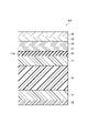
- FIG. 1 is a schematic cross-sectional view showing an example of a film heater.
- a film heater 100 of FIG. A layer 22 and an ITO layer 26 are provided in that order.
- the substrate 10, the first hard coat layer 11, the first dielectric layer 21, the metal layer 24 containing one or both of silver and silver alloy, the second dielectric layer 22, and the ITO layer 26 are as described above. be.
- the high refractive index layer 20 is a layer having a higher refractive index than the substrate 10, the first hard coat layer 11 and the first dielectric layer 21.
- the high refractive index layer 20 may be a layer (third dielectric layer) having a composition different from that of the first dielectric layer 21 .
- High refractive index layer 20 may comprise, for example, an oxide or nitride and may have a refractive index between 1.8 and 2.5. By providing such a high refractive index layer 20, the reflectance of visible light on the substrate 10 side can be sufficiently reduced.
- the high refractive index layer 20 is selected from silicon nitride, niobium oxide, and titanium oxide from the viewpoint of improving adhesion to the first dielectric layer 21 while sufficiently reducing the reflectance of visible light on the base material 10 side. may contain at least one
- the high refractive index layer 20 preferably contains silicon nitride. This increases the affinity with the silica filler contained in the first hard coat layer 11 . Therefore, the adhesion between the first hard coat layer 11 and the high refractive index layer 20 is enhanced, and the durability of the film heater can be further improved.
- the thickness of the high refractive index layer 20 is, for example, 5 to 40 nm, preferably 10 to 30 nm, from the viewpoint of reducing both the reflectance and transmittance of visible light in a well-balanced manner.
- the high refractive index layer 20 can be formed using DC magnetron sputtering, for example.
- the film formation method of the high refractive index layer 20 is not particularly limited, and it may be formed by other vacuum film formation methods using plasma, ion beam, or the like. Such a high refractive index layer 20 has a smooth surface.
- the peak intensity of Si element K ⁇ rays detected by the fluorescent X-ray analysis of the surface 11A of the first hard coat layer 11 is 15 to 35 cps.
- the silica filler is sufficiently exposed on such a surface 11A. Therefore, even if the surface of the layer (high refractive index layer 20) with which the surface 11A of the first hard coat layer 11 contacts is smooth, the first hard coat layer 11 and the high refractive index layer 20 in direct contact therewith can sufficiently maintain the adhesion of. Therefore, the durability of the film heater 100 can be sufficiently increased.
- a portion of the ITO layer 26, a portion of the second dielectric layer 22, and a portion of the metal layer 24 in the film heater 100 may be removed by etching or the like.
- the metal layer 24, the second dielectric layer 22 and the ITO layer 26 form a conductor pattern.
- a portion of the first dielectric layer 21 may also be removed by etching or the like.
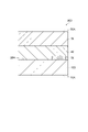
- FIG. 2 is a schematic cross-sectional view showing another example of the film heater.
- the film heater 101 in FIG. 2 has a first hard coat layer 11, a high refractive index layer 20, a first dielectric layer 21, silver and silver on one surface of the substrate 10, similar to the film heater 100 in FIG.
- a metal layer 24 comprising one or both of the alloys, a second dielectric layer 22 and an ITO layer 26 are provided in that order. These configurations are as described above.
- the film heater 101 of FIG. 2 has the second hard coat layer 12 and the low-reflection layer 28 in this order from the substrate 10 side on the other surface of the substrate 10 .
- the second hard coat layer 12 may contain the same components as the first hard coat layer 11 .
- it may contain a resin component (second resin component) obtained by curing a resin composition and a filler dispersed in the resin component.
- the second resin component include those similar to those of the first resin component.
- the filler contained in the second hard coat layer 12 may be the same silica filler as the first hard coat layer 11, or may be a filler different from the silica filler.
- the filler content in the second hard coat layer 12 may be the same as or different from that in the first hard coat layer 11 . May not contain fillers.
- the resin component in the second hard coat layer 12 may be the same as or different from that in the first hard coat layer 11 .
- the second hard coat layer 12 can be formed by the same method as the first hard coat layer 11 .
- the thickness of the second hard coat layer 12 may be, for example, 0.1 to 10 ⁇ m, or may be 0.5 to 5 ⁇ m. As a result, the adhesion between the second hard coat layer 12 and the layer in direct contact therewith (for example, the low-reflection layer 28) can be sufficiently enhanced, and the occurrence of thickness unevenness and wrinkles can be sufficiently suppressed. .
- the refractive index of the second hard coat layer 12 may be, for example, 1.40 to 1.60.
- the absolute value of the difference in refractive index between the substrate 10 and the second hard coat layer 12 may be, for example, 0.1 or less.
- the low-reflection layer 28 reduces reflection of visible light that enters the film heater 101 from one side (ITO layer 26) of the substrate 10 and exits from the other side (low-reflection layer 28) of the substrate 10. It is a layer that has the function of That is, the low-reflection layer 28 forming the other surface of the film heater 101 has a refractive index lower than that of the substrate 10 and the second hard coat layer 12 and higher than that of air. This makes it possible to increase the visible light transmittance of the film heater 101 and achieve even higher transparency.
- the refractive index of the low-reflection layer 28 may be, for example, 1.1 to 1.4.
- the low-reflection layer 28 may contain, for example, a resin component obtained by curing a resin composition and a filler dispersed in the resin component.
- the filler is preferably hollow. Thereby, the refractive index can be made lower than that of the second hard coat layer 12 and the substrate 10 .
- the filler may be a hollow silica filler.
- the resin component may contain an acrylic resin.
- the thickness of the low-reflection layer 28 may be 10-300 nm, 30-200 nm, or 50-150 nm. Thereby, reflection can be sufficiently suppressed while the thickness of the film heater 101 is kept thin.
- film heater in the present disclosure is not limited to the examples of FIGS. 1 and 2.
- film heaters 100 and 101 may each comprise any other layer.
- the film heater 101 does not have to include at least one of the second hard coat layer 12 and the low reflection layer 28 .
- the film heater 100 may have at least one of the second hard coat layer 12 and the low reflection layer 28 .
- the visible light absorptivity of the film heaters 100 and 101 is, for example, 10.3% or less. Thereby, the visible light transmittance can be increased to, for example, 80% or more. Also, the surface resistivity of the ITO layer 26 of the film heaters 100, 101 is, for example, 5 to 30 ⁇ /sq. and 10-20 ⁇ /sq. may be Such a film heater is suitably used for vehicle glass (for example, windshield and rear glass) that are required to have high transparency and excellent defrosting performance and defogging performance.
- vehicle glass for example, windshield and rear glass
- FIG. 3 is a schematic cross-sectional view showing an example of glass with a heater.
- the heater-equipped glass 200 shown in FIG. 3 includes the film heater 100 shown in FIG. , provided.
- a portion of the surface 26A on the ITO layer side is covered with an electrode 60.
- the electrodes 60 may be formed, for example, by applying silver paste to the surface 26A. After providing the electrode 60 so as to partially cover the surface 26A of the ITO layer in this manner, an adhesive is applied so as to cover the surface 26A of the ITO layer and the electrode 60, and the adhesive is applied so as to face the surface 26A and the electrode 60.
- a glass plate 50 is placed. After that, the glass plate 50, the surface 26A and the electrode 60 are pressed against each other to obtain the glass 200 with the heater.
- the adhesive forming the adhesive layer 40 may be optical glue, for example.
- the electrodes 60 are provided in pairs, and are connected to a power source (not shown) to energize the film heater 100 to generate heat.
- a power source not shown
- ice, frost, etc. adhering to the surface 50A of the glass plate 50 can be removed.
- Water droplets (fogging) adhering to the surface 10A opposite to the surface 26A of the film heater 100 on the ITO layer 26 side can also be removed smoothly.
- the temperature rise width ( ⁇ T) of the film heater 100 may be 20 to 45° C., or may be 25 to 40° C., based on the temperature before the temperature rise. As a result, it is possible to suppress an excessive temperature rise on the surface 10A while maintaining a sufficiently high performance of removing ice, frost, etc. on the surface 50A.
- the surface resistivity of the film heater is preferably 5 to 30 ⁇ /sq. and more preferably 10 to 20 ⁇ /sq. is.
- the heater-equipped glass 200 includes the film heater 100 in the example of FIG. 3, it is not limited to this.
- the film heater 101 of FIG. 2 may be provided, or a modification thereof may be provided.
- a variation of film heater 100 or a variation of film heater 101 may include an IZO layer instead of ITO layer 26 .
- an electrode 60 may be provided so as to partially cover the surface of the IZO layer to form glass with a heater.
- the present disclosure includes the following contents [1] to [5].
- a substrate a first hard coat layer containing a first resin component and a silica filler, a first dielectric layer, a metal layer containing one or both of silver and a silver alloy, and a second dielectric layer , an ITO layer or an IZO layer in this order
- the metal layer has a thickness of 5.5 to 7.5 nm
- a film heater having a peak intensity of 15 to 35 cps indicating a K ⁇ ray of Si element detected by fluorescent X-ray analysis of the surface of the first hard coat layer on the first dielectric layer side.
- a second hard coat layer containing a second resin component and a low-reflection layer are provided in this order from the base material side on the side opposite to the first hard coat layer side of the base material,
- Example 1 A polyethylene terephthalate (PET) film having a thickness of 125 ⁇ m was prepared as a base material. A first hard coat layer was formed on one surface of the PET film. Specifically, a silica filler (average particle size: 100 nm, manufactured by CIK Nanotech, trade name: AB-S53), a resin composition containing an acrylic monomer (curable compound) and a photopolymerization initiator, and a solvent was blended to prepare a paint. Z-737-9AL (trade name) manufactured by Aica Kogyo Co., Ltd.
- the content of the photopolymerization initiator based on the mass of the resin composition was 5% by mass.
- the solvent content, based on the weight of the paint, was 80% by weight.
- the viscosity of the paint (20° C.) was 0.9 mPa ⁇ .
- This paint was applied on one side of the PET film, dried, and cured by irradiation with ultraviolet rays to form the first hard coat layer.
- the content of the silica filler relative to the resin component in the first hard coat layer which is calculated from the compounding amount of the resin composition (monomer + Kojugo initiator) and the compounding amount of the silica filler in the paint, was 12% by mass.
- a high refractive index layer was formed on the first hard coat layer by DC magnetron sputtering.
- This high refractive index layer was formed using a boron-doped Si target in a mixed atmosphere containing 80% by volume of argon gas and 20% by volume of nitrogen gas.
- the high refractive index layer thus formed was composed of SiN.
- the refractive index of the high refractive index layer was 1.9.
- a first dielectric layer, a metal layer containing a silver alloy, a second dielectric layer, and an ITO layer were formed in this order on the high refractive index layer.
- a first dielectric layer was formed using a ZnO--In 2 O 3 --TiO 2 target, and a second dielectric layer was formed using a ZnO--In 2 O 3 --TiO 2 --SnO 2 target.
- the composition (molar ratio) of each target was as shown in Table 1.
- the first dielectric layer and the second dielectric layer each had the same composition as the target.
- a metal layer was formed using an Ag--Pd--Cu target.
- the metal layer had the same composition as the target.
- the ITO layer had approximately the same composition as the ITO target.
- a film heater having a PET substrate, a first hard coat layer, a high refractive index layer, a first dielectric layer, a metal layer, a second dielectric layer, and an ITO layer in this order was obtained.
- the obtained film heater was cut along the stacking direction using a focused ion beam device (FIB). The cut surface was observed with a transmission electron microscope to determine the thickness of each layer.
- the thickness of the first hard coat layer was 1.5 ⁇ m
- the thickness of the high refractive index layer was 20 nm
- the thickness of the first dielectric layer was 10 nm
- the thickness of the metal layer was 6 nm
- the thickness of the second dielectric layer was 6 nm.
- the thickness of the ITO layer was 20 nm.
- Examples 2 to 7, Comparative Examples 1 to 4 Same as Example 1, except that the output of DC magnetron sputtering was adjusted to change the thickness of the metal layer and/or the blending amount of the silica filler used in forming the first hard coat layer was changed. Then, film heaters for each example and each comparative example were produced. In the same manner as in Example 1, the thickness of the metal layer and the content of the silica filler in the first hard coat layer in the film heaters of each example and each comparative example were determined. Table 2 shows the results.
- the adhered cellophane tape was peeled off, the state of peeling in 100 squares was visually confirmed, and the results were classified into six grades of 5B, 4B, 3B, 2B, 1B, and 0B. Between the high refractive index layer and the first hard coat layer, the case where there was no peeling was classified as "5B", and the case where the ratio of the peeled region was the highest was classified as "0B". The measurement results were as shown in Table 2.
- the visible light absorptances of the film heaters of Comparative Example 1 in which the thickness of the metal layer is less than 5.5 nm, and Comparative Example 2, in which the thickness of the metal layer exceeds 7.5 nm, are the target values. It exceeded a certain 10.3%. Moreover, in Comparative Example 1, the surface resistivity was high, and ⁇ T tended to be too small. In Comparative Example 2, the surface resistivity was low and ⁇ T tended to be too large.
- Comparative Example 3 in which the peak intensity of the K ⁇ ray of the silicon element was too small, the adhesion between the first hard coat layer and the high refractive index layer was lowered, and it was confirmed that the durability was insufficient. rice field. This is probably because less silica filler is exposed on the surface of the first hard coat layer (the interface between the first hard coat layer and the high refractive index layer).
- the absorptance of visible light in Comparative Example 4 in which the intensity of fluorescent X-rays was excessive, exceeded the target value of 10.3%. This is presumed to be due to the excessive silica filler content.
- the absorption rate of visible light was sufficiently small, and the adhesion between the high refractive index layer and the first hard coat layer was sufficiently excellent. It was also confirmed that ⁇ T is in an appropriate range and is useful in many applications.
- a film heater that has excellent durability and is capable of sufficiently reducing the absorptance of visible light. Also provided is glass with a heater, which has a film heater that is excellent in durability and capable of sufficiently reducing the absorptance of visible light.
- SYMBOLS 10 Base material 10A, 11A, 26A, 50A... Surface 11... First hard coat layer 12... Second hard coat layer 20... High refractive index layer 21... First dielectric layer 22... Second Dielectric layer 24 Metal layer 26 ITO layer 28 Low reflection layer 40 Adhesive layer 50 Glass plate 60 Electrode 100, 101 Film heater 200 Glass with heater.
Landscapes
- Laminated Bodies (AREA)
Priority Applications (3)
| Application Number | Priority Date | Filing Date | Title |
|---|---|---|---|
| CN202280029990.4A CN117204119A (zh) | 2021-04-26 | 2022-04-25 | 薄膜加热器和带加热器的玻璃 |
| JP2023517509A JP7837954B2 (ja) | 2021-04-26 | 2022-04-25 | フィルムヒータ、及び、ヒータ付きガラス |
| US18/288,247 US20240215120A1 (en) | 2021-04-26 | 2022-04-25 | Film heater and heater-equipped glass |
Applications Claiming Priority (2)
| Application Number | Priority Date | Filing Date | Title |
|---|---|---|---|
| JP2021-074132 | 2021-04-26 | ||
| JP2021074132 | 2021-04-26 |
Publications (1)
| Publication Number | Publication Date |
|---|---|
| WO2022230810A1 true WO2022230810A1 (ja) | 2022-11-03 |
Family
ID=83847191
Family Applications (1)
| Application Number | Title | Priority Date | Filing Date |
|---|---|---|---|
| PCT/JP2022/018733 Ceased WO2022230810A1 (ja) | 2021-04-26 | 2022-04-25 | フィルムヒータ、及び、ヒータ付きガラス |
Country Status (4)
| Country | Link |
|---|---|
| US (1) | US20240215120A1 (cg-RX-API-DMAC7.html) |
| JP (1) | JP7837954B2 (cg-RX-API-DMAC7.html) |
| CN (1) | CN117204119A (cg-RX-API-DMAC7.html) |
| WO (1) | WO2022230810A1 (cg-RX-API-DMAC7.html) |
Citations (6)
| Publication number | Priority date | Publication date | Assignee | Title |
|---|---|---|---|---|
| JPH0963754A (ja) * | 1995-06-15 | 1997-03-07 | Mitsui Toatsu Chem Inc | 耐久性透明面状ヒーター及びその製造方法 |
| JP2004031241A (ja) * | 2002-06-27 | 2004-01-29 | Kyocera Corp | セラミックヒータ及びその製造方法 |
| JP2018020771A (ja) * | 2016-07-25 | 2018-02-08 | 日本板硝子株式会社 | ウインドシールドおよびその製造方法 |
| WO2020022270A1 (ja) * | 2018-07-24 | 2020-01-30 | Tdk株式会社 | ヒータ用透明導電フィルム及びヒータ |
| JP2020082513A (ja) * | 2018-11-26 | 2020-06-04 | Tdk株式会社 | 透明導電体、調光体及び透明発熱体 |
| JP2020167047A (ja) * | 2019-03-29 | 2020-10-08 | 日東電工株式会社 | ヒータ |
Family Cites Families (3)
| Publication number | Priority date | Publication date | Assignee | Title |
|---|---|---|---|---|
| US5911899A (en) * | 1995-06-15 | 1999-06-15 | Mitsui Chemicals, Inc. | Corrosion-proof transparent heater panels and preparation process thereof |
| PL2803245T3 (pl) * | 2012-01-10 | 2017-08-31 | Saint-Gobain Glass France | Przezroczysta szyba o powłoce przewodzącej prąd elektryczny |
| KR20170024830A (ko) * | 2015-08-26 | 2017-03-08 | 전자부품연구원 | 단열기능이 있는 스마트 윈도우 코팅 |
-
2022
- 2022-04-25 WO PCT/JP2022/018733 patent/WO2022230810A1/ja not_active Ceased
- 2022-04-25 US US18/288,247 patent/US20240215120A1/en active Pending
- 2022-04-25 JP JP2023517509A patent/JP7837954B2/ja active Active
- 2022-04-25 CN CN202280029990.4A patent/CN117204119A/zh active Pending
Patent Citations (6)
| Publication number | Priority date | Publication date | Assignee | Title |
|---|---|---|---|---|
| JPH0963754A (ja) * | 1995-06-15 | 1997-03-07 | Mitsui Toatsu Chem Inc | 耐久性透明面状ヒーター及びその製造方法 |
| JP2004031241A (ja) * | 2002-06-27 | 2004-01-29 | Kyocera Corp | セラミックヒータ及びその製造方法 |
| JP2018020771A (ja) * | 2016-07-25 | 2018-02-08 | 日本板硝子株式会社 | ウインドシールドおよびその製造方法 |
| WO2020022270A1 (ja) * | 2018-07-24 | 2020-01-30 | Tdk株式会社 | ヒータ用透明導電フィルム及びヒータ |
| JP2020082513A (ja) * | 2018-11-26 | 2020-06-04 | Tdk株式会社 | 透明導電体、調光体及び透明発熱体 |
| JP2020167047A (ja) * | 2019-03-29 | 2020-10-08 | 日東電工株式会社 | ヒータ |
Also Published As
| Publication number | Publication date |
|---|---|
| CN117204119A (zh) | 2023-12-08 |
| JPWO2022230810A1 (cg-RX-API-DMAC7.html) | 2022-11-03 |
| JP7837954B2 (ja) | 2026-03-31 |
| US20240215120A1 (en) | 2024-06-27 |
Similar Documents
| Publication | Publication Date | Title |
|---|---|---|
| JP6601199B2 (ja) | 透明導電体 | |
| WO2020022270A1 (ja) | ヒータ用透明導電フィルム及びヒータ | |
| US9582130B2 (en) | Transparent conductor and touch panel | |
| KR20130099213A (ko) | 투명 도전성 필름 및 그 제조 방법 | |
| KR20160146638A (ko) | 투명 도전성 필름 | |
| JP6048526B2 (ja) | 透明導電体及びタッチパネル | |
| JP7046497B2 (ja) | 液晶調光部材、光透過性導電フィルム、および液晶調光素子 | |
| WO2015046519A1 (ja) | 導電性積層体およびそれを用いるタッチパネル | |
| JP2018124449A (ja) | 調光体用の積層体、及び調光体 | |
| JP6260647B2 (ja) | 透明導電体 | |
| JP6739310B2 (ja) | 光透過性導電フィルム、その製造方法、調光フィルムおよびその製造方法 | |
| JP6923415B2 (ja) | 透明導電性フィルムおよび透明導電性フィルム積層体 | |
| JP6409588B2 (ja) | 透明導電体及びタッチパネル | |
| JP7837954B2 (ja) | フィルムヒータ、及び、ヒータ付きガラス | |
| JP7716172B2 (ja) | 透明導電性フィルム | |
| JP2018022634A (ja) | 透明導電体 | |
| JP2016110899A (ja) | 透明導電体及びタッチパネル | |
| JP7225734B2 (ja) | 透明導電体、調光体及び透明発熱体 | |
| JP7784421B2 (ja) | フィルムヒータ、及び、ヒータ付きガラス | |
| JP7861545B2 (ja) | 接着層付き機能性フィルムおよびガラス積層体 | |
| JP3681280B2 (ja) | ディスプレイ用光学フィルター | |
| JP7024852B2 (ja) | 透明導電体、調光体及び透明発熱体 | |
| KR102187987B1 (ko) | 다층 박막 구조를 갖는 투명 히터용 전극 | |
| JP2019188768A (ja) | ハードコートフィルム、透明導電性フィルム、透明導電性フィルム積層体および画像表示装置 | |
| JP2018051893A (ja) | 透明導電体 |
Legal Events
| Date | Code | Title | Description |
|---|---|---|---|
| 121 | Ep: the epo has been informed by wipo that ep was designated in this application |
Ref document number: 22795723 Country of ref document: EP Kind code of ref document: A1 |
|
| WWE | Wipo information: entry into national phase |
Ref document number: 2023517509 Country of ref document: JP |
|
| WWE | Wipo information: entry into national phase |
Ref document number: 202280029990.4 Country of ref document: CN |
|
| WWE | Wipo information: entry into national phase |
Ref document number: 18288247 Country of ref document: US |
|
| NENP | Non-entry into the national phase |
Ref country code: DE |
|
| 122 | Ep: pct application non-entry in european phase |
Ref document number: 22795723 Country of ref document: EP Kind code of ref document: A1 |