WO2022230505A1 - 高分子フィルムの剥離方法、電子デバイスの製造方法、及び、剥離装置 - Google Patents
高分子フィルムの剥離方法、電子デバイスの製造方法、及び、剥離装置 Download PDFInfo
- Publication number
- WO2022230505A1 WO2022230505A1 PCT/JP2022/014586 JP2022014586W WO2022230505A1 WO 2022230505 A1 WO2022230505 A1 WO 2022230505A1 JP 2022014586 W JP2022014586 W JP 2022014586W WO 2022230505 A1 WO2022230505 A1 WO 2022230505A1
- Authority
- WO
- WIPO (PCT)
- Prior art keywords
- polymer film
- inorganic substrate
- laminate
- peeling
- film
- Prior art date
- Legal status (The legal status is an assumption and is not a legal conclusion. Google has not performed a legal analysis and makes no representation as to the accuracy of the status listed.)
- Ceased
Links
Images







Classifications
-
- H—ELECTRICITY
- H10—SEMICONDUCTOR DEVICES; ELECTRIC SOLID-STATE DEVICES NOT OTHERWISE PROVIDED FOR
- H10W—GENERIC PACKAGES, INTERCONNECTIONS, CONNECTORS OR OTHER CONSTRUCTIONAL DETAILS OF DEVICES COVERED BY CLASS H10
- H10W74/00—Encapsulations, e.g. protective coatings
- H10W74/01—Manufacture or treatment
- H10W74/016—Manufacture or treatment using moulds
- H10W74/017—Auxiliary layers for moulds, e.g. release layers or layers preventing residue
-
- H—ELECTRICITY
- H10—SEMICONDUCTOR DEVICES; ELECTRIC SOLID-STATE DEVICES NOT OTHERWISE PROVIDED FOR
- H10P—GENERIC PROCESSES OR APPARATUS FOR THE MANUFACTURE OR TREATMENT OF DEVICES COVERED BY CLASS H10
- H10P72/00—Handling or holding of wafers, substrates or devices during manufacture or treatment thereof
- H10P72/04—Apparatus for manufacture or treatment
- H10P72/0442—Apparatus for placing on an insulating substrate, e.g. tape
-
- B—PERFORMING OPERATIONS; TRANSPORTING
- B29—WORKING OF PLASTICS; WORKING OF SUBSTANCES IN A PLASTIC STATE IN GENERAL
- B29C—SHAPING OR JOINING OF PLASTICS; SHAPING OF MATERIAL IN A PLASTIC STATE, NOT OTHERWISE PROVIDED FOR; AFTER-TREATMENT OF THE SHAPED PRODUCTS, e.g. REPAIRING
- B29C69/00—Combinations of shaping techniques not provided for in a single one of main groups B29C39/00 - B29C67/00, e.g. associations of moulding and joining techniques; Apparatus therefore
-
- B—PERFORMING OPERATIONS; TRANSPORTING
- B32—LAYERED PRODUCTS
- B32B—LAYERED PRODUCTS, i.e. PRODUCTS BUILT-UP OF STRATA OF FLAT OR NON-FLAT, e.g. CELLULAR OR HONEYCOMB, FORM
- B32B43/00—Operations specially adapted for layered products and not otherwise provided for, e.g. repairing; Apparatus therefor
- B32B43/006—Delaminating
-
- B—PERFORMING OPERATIONS; TRANSPORTING
- B65—CONVEYING; PACKING; STORING; HANDLING THIN OR FILAMENTARY MATERIAL
- B65H—HANDLING THIN OR FILAMENTARY MATERIAL, e.g. SHEETS, WEBS, CABLES
- B65H29/00—Delivering or advancing articles from machines; Advancing articles to or into piles
- B65H29/54—Article strippers, e.g. for stripping from advancing elements
-
- B—PERFORMING OPERATIONS; TRANSPORTING
- B65—CONVEYING; PACKING; STORING; HANDLING THIN OR FILAMENTARY MATERIAL
- B65H—HANDLING THIN OR FILAMENTARY MATERIAL, e.g. SHEETS, WEBS, CABLES
- B65H41/00—Machines for separating superposed webs
-
- H—ELECTRICITY
- H05—ELECTRIC TECHNIQUES NOT OTHERWISE PROVIDED FOR
- H05K—PRINTED CIRCUITS; CASINGS OR CONSTRUCTIONAL DETAILS OF ELECTRIC APPARATUS; MANUFACTURE OF ASSEMBLAGES OF ELECTRICAL COMPONENTS
- H05K3/00—Apparatus or processes for manufacturing printed circuits
- H05K3/22—Secondary treatment of printed circuits
- H05K3/28—Applying non-metallic protective coatings
- H05K3/288—Removal of non-metallic coatings, e.g. for repairing
-
- H—ELECTRICITY
- H10—SEMICONDUCTOR DEVICES; ELECTRIC SOLID-STATE DEVICES NOT OTHERWISE PROVIDED FOR
- H10P—GENERIC PROCESSES OR APPARATUS FOR THE MANUFACTURE OR TREATMENT OF DEVICES COVERED BY CLASS H10
- H10P14/00—Formation of materials, e.g. in the shape of layers or pillars
- H10P14/60—Formation of materials, e.g. in the shape of layers or pillars of insulating materials
- H10P14/66—Formation of materials, e.g. in the shape of layers or pillars of insulating materials characterised by the type of materials
- H10P14/662—Laminate layers, e.g. stacks of alternating high-k metal oxides
-
- H—ELECTRICITY
- H10—SEMICONDUCTOR DEVICES; ELECTRIC SOLID-STATE DEVICES NOT OTHERWISE PROVIDED FOR
- H10P—GENERIC PROCESSES OR APPARATUS FOR THE MANUFACTURE OR TREATMENT OF DEVICES COVERED BY CLASS H10
- H10P72/00—Handling or holding of wafers, substrates or devices during manufacture or treatment thereof
- H10P72/04—Apparatus for manufacture or treatment
- H10P72/0428—Apparatus for mechanical treatment or grinding or cutting
-
- H—ELECTRICITY
- H10—SEMICONDUCTOR DEVICES; ELECTRIC SOLID-STATE DEVICES NOT OTHERWISE PROVIDED FOR
- H10P—GENERIC PROCESSES OR APPARATUS FOR THE MANUFACTURE OR TREATMENT OF DEVICES COVERED BY CLASS H10
- H10P72/00—Handling or holding of wafers, substrates or devices during manufacture or treatment thereof
- H10P72/04—Apparatus for manufacture or treatment
- H10P72/0441—Apparatus for sealing, encapsulating, glassing, decapsulating or the like
-
- H—ELECTRICITY
- H10—SEMICONDUCTOR DEVICES; ELECTRIC SOLID-STATE DEVICES NOT OTHERWISE PROVIDED FOR
- H10P—GENERIC PROCESSES OR APPARATUS FOR THE MANUFACTURE OR TREATMENT OF DEVICES COVERED BY CLASS H10
- H10P72/00—Handling or holding of wafers, substrates or devices during manufacture or treatment thereof
- H10P72/70—Handling or holding of wafers, substrates or devices during manufacture or treatment thereof for supporting or gripping
- H10P72/74—Handling or holding of wafers, substrates or devices during manufacture or treatment thereof for supporting or gripping using temporarily an auxiliary support
-
- H—ELECTRICITY
- H10—SEMICONDUCTOR DEVICES; ELECTRIC SOLID-STATE DEVICES NOT OTHERWISE PROVIDED FOR
- H10P—GENERIC PROCESSES OR APPARATUS FOR THE MANUFACTURE OR TREATMENT OF DEVICES COVERED BY CLASS H10
- H10P72/00—Handling or holding of wafers, substrates or devices during manufacture or treatment thereof
- H10P72/70—Handling or holding of wafers, substrates or devices during manufacture or treatment thereof for supporting or gripping
- H10P72/74—Handling or holding of wafers, substrates or devices during manufacture or treatment thereof for supporting or gripping using temporarily an auxiliary support
- H10P72/744—Details of chemical or physical process used for separating the auxiliary support from a device or a wafer
-
- H—ELECTRICITY
- H10—SEMICONDUCTOR DEVICES; ELECTRIC SOLID-STATE DEVICES NOT OTHERWISE PROVIDED FOR
- H10P—GENERIC PROCESSES OR APPARATUS FOR THE MANUFACTURE OR TREATMENT OF DEVICES COVERED BY CLASS H10
- H10P72/00—Handling or holding of wafers, substrates or devices during manufacture or treatment thereof
- H10P72/70—Handling or holding of wafers, substrates or devices during manufacture or treatment thereof for supporting or gripping
- H10P72/78—Handling or holding of wafers, substrates or devices during manufacture or treatment thereof for supporting or gripping using vacuum or suction, e.g. Bernoulli chucks
-
- B—PERFORMING OPERATIONS; TRANSPORTING
- B65—CONVEYING; PACKING; STORING; HANDLING THIN OR FILAMENTARY MATERIAL
- B65H—HANDLING THIN OR FILAMENTARY MATERIAL, e.g. SHEETS, WEBS, CABLES
- B65H2301/00—Handling processes for sheets or webs
- B65H2301/50—Auxiliary process performed during handling process
- B65H2301/51—Modifying a characteristic of handled material
- B65H2301/511—Processing surface of handled material upon transport or guiding thereof, e.g. cleaning
- B65H2301/5112—Processing surface of handled material upon transport or guiding thereof, e.g. cleaning removing material from outer surface
- B65H2301/51122—Processing surface of handled material upon transport or guiding thereof, e.g. cleaning removing material from outer surface peeling layer of material
-
- B—PERFORMING OPERATIONS; TRANSPORTING
- B65—CONVEYING; PACKING; STORING; HANDLING THIN OR FILAMENTARY MATERIAL
- B65H—HANDLING THIN OR FILAMENTARY MATERIAL, e.g. SHEETS, WEBS, CABLES
- B65H2406/00—Means using fluid
- B65H2406/30—Suction means
- B65H2406/35—Other elements with suction surface, e.g. plate or wall
- B65H2406/351—Other elements with suction surface, e.g. plate or wall facing the surface of the handled material
-
- B—PERFORMING OPERATIONS; TRANSPORTING
- B65—CONVEYING; PACKING; STORING; HANDLING THIN OR FILAMENTARY MATERIAL
- B65H—HANDLING THIN OR FILAMENTARY MATERIAL, e.g. SHEETS, WEBS, CABLES
- B65H2701/00—Handled material; Storage means
- B65H2701/10—Handled articles or webs
- B65H2701/17—Nature of material
- B65H2701/172—Composite material
- B65H2701/1726—Composite material including detachable components
-
- B—PERFORMING OPERATIONS; TRANSPORTING
- B65—CONVEYING; PACKING; STORING; HANDLING THIN OR FILAMENTARY MATERIAL
- B65H—HANDLING THIN OR FILAMENTARY MATERIAL, e.g. SHEETS, WEBS, CABLES
- B65H2701/00—Handled material; Storage means
- B65H2701/10—Handled articles or webs
- B65H2701/17—Nature of material
- B65H2701/175—Plastic
- B65H2701/1752—Polymer film
Definitions
- the present invention relates to a polymer film peeling method, an electronic device manufacturing method, and a peeling apparatus.
- Patent Documents 1 Conventionally, as a method for peeling a polymer film from a support, a method of weakening the adhesion between the polymer film and the support by irradiating laser light is known (see, for example, Patent Documents 1). In addition, various methods for facilitating this laser peeling have been studied. (See Patent Document 2, for example). A method for mechanically peeling the film has also been investigated. (See Patent Document 3, for example).
- Patent Document 2 It is feared that Mechanical detachment also affects the quality of the polymer film itself due to stress damage caused by the deformation of the polymer film, the circuits and devices formed on the surface of the polymer film, and the elements mounted on the polymer film. has been a concern.
- the method of Patent Document 2 is complicated because it requires a step such as forming a layer between the support and the polyimide film in advance to facilitate peeling. In the method of Patent Document 3, it is still difficult to prevent defects from occurring in the device due to the mechanical method.
- the present invention has been made in view of the above-mentioned problems, and its object is to affect the quality of polymer films, circuits and devices formed on the surface of polymer films, and elements mounted on polymer films. It is an object of the present invention to provide a method for peeling a polymer film, a method for manufacturing an electronic device, and a peeling apparatus that can easily peel a polymer film from an inorganic substrate without removing the film.
- the present inventor has conducted intensive research on polymer film peeling methods, electronic device manufacturing methods, and peeling devices.
- the polymer film can be easily formed without affecting the quality of the polymer film, the circuits and devices formed on the surface of the polymer film, and the elements mounted on the polymer film. can be peeled off from the inorganic substrate, and have completed the present invention.
- the present invention provides the following.
- a first method for peeling a polymer film comprising Step C.
- a partition wall is provided on the side surface of the laminate, a second polymer film larger than the inorganic substrate is laminated on the inorganic substrate surface of the laminate, and the second polymer film and the third polymer film are laminated.
- Step C to do A first polymer film peeling method comprising: [3] The step C is [1] or [2], wherein the pressure in the sealed space is made higher than the pressure outside the sealed space by 0.02 atm or more by injecting gas into the peeling portion. 1. The method for peeling the polymer film. [4] The first polymer film peeling method according to any one of [1] to [3], wherein an adhesive protective film is laminated on the surface of the vacuum suction plate.
- a restricting plate for restricting deformation of the inorganic substrate is provided on the opposite side of the second polymer film to the inorganic substrate, and a gap between the restricting plate and the second polymer film is provided.
- the first polymer film peeling method according to any one of [1] to [7], wherein the thickness is 0.5 mm or more and 5 mm or less.
- a restricting plate for restricting deformation of the inorganic substrate is provided on the opposite side of the second polymer film to the inorganic substrate, and the restricting plate and the second polymer film are in contact with each other.
- the peel strength F2 between the inorganic substrate and the second polymer film and the peel strength F1 between the inorganic substrate and the first polymer film are: 2 ⁇ F1 ⁇ F2
- the peel strength F1 of the molecular film is 2 ⁇ F1 ⁇ F2 and 2 ⁇ F1 ⁇ F3
- the first polymer film peeling method according to any one of [2] to [9], wherein the relationship is: [12] Step A of preparing a laminate in which the first polymer film on which the electronic device is formed and the inorganic substrate are in close contact; The laminate is placed and fixed so that the first polymer film surface is in contact with a vacuum adsorption plate, partition walls are provided on the side surfaces of the laminate, and the inorganic substrate surface of the laminate is larger than the inorganic substrate.
- Step B1 of laminating a second polymer film and forming a closed space with the vacuum adsorption plate, the second polymer film and the partition wall; and a step C of injecting gas between the first polymer film and the inorganic substrate of the laminate to separate the first polymer film while maintaining a substantially flat surface.
- a method for producing a polymer film with an electronic device [13] Step A of preparing a laminate in which the first polymer film on which the electronic device is formed and the inorganic substrate are in close contact; A third polymer film larger than the first polymer film is laminated on the surface of the first polymer film of the laminate, and the third polymer film is placed in contact with the vacuum suction plate.
- a partition wall is provided on the side surface of the laminate, a second polymer film larger than the inorganic substrate is laminated on the inorganic substrate surface of the laminate, and the second polymer film and the third polymer film are laminated.
- a peeling device for peeling the first polymer film from the inorganic substrate from the laminate in which the first polymer film on which the electronic device is formed and the inorganic substrate are in close contact, pressure applying means for applying pressure to the peeled portion between the first polymer film provided at the end of the laminate and the inorganic substrate; means for providing a sealed space by placing a vacuum adsorption plate on the first polymer film surface of the laminate, partition walls on the side surface, and a second polymer film larger than the inorganic substrate on the inorganic substrate surface;
- a peeling device comprising means for fixing said first polymer film substantially flat during peeling.
- the polymer film is peeled from the inorganic substrate by injecting gas into the peeling portion and applying pressure instead of mechanically peeling, and the polymer film is not bent. Since it is peeled (substantially flat), it is possible to easily peel the polymer film from the inorganic substrate without affecting the quality of the polymer film.
- the quality of the electronic device including wiring and thin film devices formed on the surface of the polymer film, and the functional element mounted on the polymer film, It becomes possible to easily peel the polymer film from the inorganic substrate.
- FIG. 1 is a schematic cross-sectional view showing an example of a laminate.
- FIG. 2-1(1) is a schematic cross-sectional view of the peeling device according to the first embodiment.
- FIG. 2-1(1) shows a state in which the peeling device is in the process of being set, and the second polymer film is placed on the partition walls.
- FIG. 2-1(2) is a schematic cross-sectional view of the peeling device according to the first embodiment.
- FIG. 2-1(2) shows the peeling device in the middle of setting, in which the laminate is fixed to the vacuum suction plate.
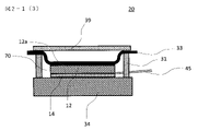
- FIG. 2-1(3) is a schematic cross-sectional view of the peeling device according to the first embodiment.
- FIG. 2-1 (3) shows the state in which the setting is completed.
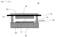
- FIG. 2-1(4) is a schematic cross-sectional view of the peeling device according to the first embodiment.
- FIG. 2-1(4) shows the state after peeling is completed.
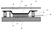
- FIG. 2-2 is a schematic cross-sectional view of a peeling device different from FIG. 2-1 according to the first embodiment.
- FIG. 2-2 is during the setting of the peeling device.
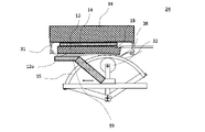
- FIG. 2-3 is a schematic cross-sectional view immediately before the peeling operation of the peeling device different from FIGS. 2-1 and 2-2 according to the first embodiment.
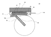
- FIG. 3-1 is a schematic cross-sectional view of a peeling device according to the second embodiment.
- FIG. 3-1 is a schematic cross-sectional view of the peeling device immediately before peeling.
- FIG. 3-2 is a schematic cross-sectional view of a peeling device different from FIG.
- FIG. 3-2 is a schematic cross-sectional view of the peeling device immediately before peeling.
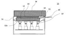
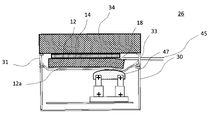
- FIG. 4-1 is a schematic cross-sectional view of the peeling device according to the third embodiment immediately before peeling.
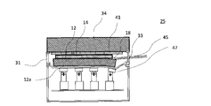
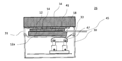
- FIG. 4-2 is a schematic cross-sectional view of a peeling device immediately before peeling, which is different from that shown in FIG. 4-1 according to the third embodiment.
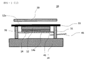
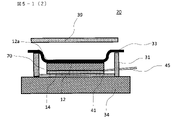
- FIG. 5-1(1) is a schematic cross-sectional view of a peeling device according to the fourth embodiment.
- FIG. 5-1(1) shows a state in which the peeling device is in the process of being set, and the second polymer film is placed on the partition walls.
- FIG. 5-1(2) is a schematic cross-sectional view of a peeling device according to the fourth embodiment.
- FIG. 5-1(1) shows a state in which the peeling device is in the process of being set, and the second polymer film is placed on the partition walls.
- FIG. 5-1(2) is a schematic cross-sectional view of a peeling device according to the fourth
- FIG. 5-1(2) shows the peeling device in the middle of setting, in which the laminate is fixed to the vacuum suction plate.
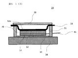
- FIG. 5-1(3) is a schematic cross-sectional view of the peeling device according to the fourth embodiment.
- FIG. 5-1(3) shows the state in which the setting is completed.
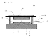
- FIG. 5-1(4) is a schematic cross-sectional view of the peeling device according to the fourth embodiment.
- FIG. 5-1(4) shows the state in which peeling is completed.
- FIG. 5-2 is a schematic cross-sectional view of a peeling device different from FIG. 5-1 according to the fourth embodiment.
- FIG. 5-2 is during the setting of the peeling device.
- FIG. 5-3 is a schematic cross-sectional view immediately before the peeling operation of the peeling device different from FIGS. 5-1 and 5-2 according to the fourth embodiment.
- FIG. 6-1 is a schematic cross-sectional view of a peeling device according to the fifth embodiment.
- FIG. 6-1 is a schematic cross-sectional view of the peeling device immediately before peeling.
- FIG. 6-2 is a schematic cross-sectional view of a peeling device different from FIG. 6-1 according to the fifth embodiment.
- FIG. 6-2 is a schematic cross-sectional view of the peeling device immediately before peeling.
- FIG. 7-1 is a schematic cross-sectional view of the peeling device according to the sixth embodiment immediately before peeling.
- FIG. 7-2 is a schematic cross-sectional view immediately before peeling of a peeling device different from that of FIG. 7-1 according to the sixth embodiment.
- FIG. 8 is a schematic cross-sectional view showing an example of a laminate with functional elements.
- FIG. 8 is a schematic cross-sectional view showing an example of a laminate with functional elements.
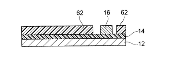
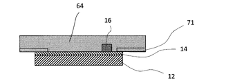
- FIG. 9 is a schematic cross-sectional view showing a state in which a spacer is provided on the first polymer film of the laminate with functional elements.
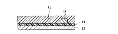
- FIG. 10 is a schematic cross-sectional view showing a state in which an embedding vacuum chuck is placed on the first polymer film of the laminate with the functional element and the functional element is embedded.
- FIG. 11 is a schematic cross-sectional view showing a state in which an embedding vacuum chuck is placed on the first polymer film of the laminate with the functional element and the functional element is embedded.
- the adhesive member is arranged on the periphery of the laminate.
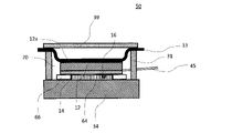
- FIG. 12 is another schematic cross-sectional view of the peeling apparatus according to the first embodiment, in which an embedding vacuum chuck is placed on the first polymer film of the laminate with the functional element, and the functional element is embedded.
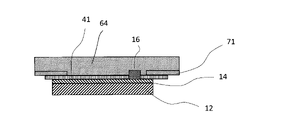
- FIG. 13 is a schematic cross-sectional view of the fourth embodiment showing a state in which an embedding vacuum chuck is placed on the first polymer film of the laminate with the functional element and the functional element is embedded.
- a third polymer film is adhered to the outer circumference of the first polymer film, and this third polymer film is in close contact with the adhesive member arranged on the outer circumference of the laminate. .
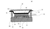
- FIG 14 is another schematic cross-sectional view of the peeling device according to the fourth embodiment, in which an embedding vacuum chuck is arranged on the first polymer film of the laminate with the functional element and the functional element is embedded.
- a third polymer film is adhered to the outer circumference of the first polymer film, and this third polymer film is in close contact with the adhesive member arranged on the outer circumference of the laminate.
- Embodiments of the present invention will be described below.
- the method for peeling the first polymer film will be described, in which the method for manufacturing an electronic device and the peeling apparatus will also be described.
- the polymer film peeling method according to the present embodiment includes the following steps A, B1 and C, or includes the following steps A, B2 and C.
- the process B1 and the process B2 may be collectively referred to as the process B. That is, step A of preparing a laminate in which a first polymer film on which an electronic device is formed and an inorganic substrate are in close contact; The laminate is placed and fixed so that the first polymer film surface is in contact with a vacuum adsorption plate, partition walls are provided on the side surfaces of the laminate, and the inorganic substrate surface of the laminate is larger than the inorganic substrate.
- a partition wall is provided on the side surface of the laminate, a second polymer film larger than the inorganic substrate is laminated on the inorganic substrate surface of the laminate, and the second polymer film and the third polymer film are laminated.
- the first polymer film since it is the first polymer film that is peeled off in the present invention, the first polymer film may be simply referred to as the "polymer film".
- FIG. 1 is a schematic cross-sectional view showing an example of a laminate.
- laminate 10 comprises inorganic substrate 12 and polymer film 14 .
- the inorganic substrate 12 and the polymer film 14 are in close contact.
- the electronic device is formed on the non-contact surface 14a of the polymer film that is not in close contact with the inorganic substrate 12.
- the inorganic substrate 12 and the polymer film 14 may be in close contact via a silane coupling agent layer, an adhesive layer, or an easily peelable layer (not shown). Also, in FIG. 1, the inorganic substrate 12 and the polymer film 14 are drawn with the same size although they have different thicknesses. The polymer film 14 and the inorganic substrate 12 have different sizes, and the polymer film 14 may be larger or smaller than the inorganic substrate 12 . Since a laminate in which the polymer film 14 is smaller than the inorganic substrate 12 is easy to produce, the sizes may differ in this way.
- the peripheral glass of the laminated body in which the polymer film 14 and the inorganic substrate 12 are in close contact with each other is cut and removed so that the polymer film 14 separates from the inorganic substrate 12 .
- the polymer film 14 may be provided with a protective film.
- the protective film size and the polymer film size may be the same, but the protective film may be smaller. It is preferable to apply the protective film before Step C, which will be described later.
- the inorganic substrate 12 may be any plate-shaped substrate that can be used as a substrate made of an inorganic substance.
- Examples of composites of plates, semiconductor wafers, and metals include laminates of these, those in which these are dispersed, and those in which these fibers are contained.
- the thickness of the inorganic substrate 12 is not particularly limited, the thickness is preferably 5 mm or less, more preferably 1.2 mm or less, and even more preferably 0.8 mm or less from the viewpoint of handleability.
- the lower limit of the thickness is not particularly limited, it is preferably 0.05 mm or more, more preferably 0.3 mm or more, and still more preferably 0.5 mm or more.
- the first polymer film 14 examples include, but are not limited to, polyimide-based resins such as polyimide, polyamideimide, polyetherimide, and fluorinated polyimide (e.g., aromatic polyimide resins and alicyclic polyimide resins); polyethylene, polypropylene, Copolyesters such as polyethylene terephthalate, polybutylene terephthalate, and polyethylene-2,6-naphthalate (for example, wholly aromatic polyesters and semi-aromatic polyesters); copolymerized (meth)acrylates typified by polymethyl methacrylate; polycarbonates; polyamides; Polysulfone; polyethersulfone; polyetherketone; cellulose acetate; cellulose nitrate; aromatic polyamide; polyvinyl chloride; Although the thickness of the first polymer film 14 is not particularly limited, it is preferably 250 ⁇ m or less, more preferably 100 ⁇ m or less, and even more preferably 50 ⁇ m or less from the viewpoint of
- the surface of the first polymer film 14 that contacts the inorganic substrate 12 is preferably subjected to surface treatment.
- the surface treatment increases the peel strength of the first polymer film.
- the surface treatment is not particularly limited, but includes plasma treatment or UV/O3 treatment , with plasma treatment being preferred.
- Plasma treatment is preferably performed for 10 seconds or longer, more preferably 30 minutes or longer, and still more preferably 1 minute or longer using a vacuum plasma treatment apparatus, for example. Also, it is preferably 30 minutes or less, more preferably 10 minutes or less, and even more preferably 5 minutes or less.
- Second polymer film 33 and third polymer film 41 are films that are larger than first polymer film 14 .
- the area of the second polymer film 33 is preferably 1.1 times or more the area of the first polymer film 14, more preferably 1.5 times or more, still more preferably 2 times. That's it. Also, it is preferably 10 times or less, more preferably 8 times or less, and still more preferably 5 times or less. By setting it within the above range, it becomes easier to create the sealed space 70 described later.
- the shape of the second polymer film 33 may be a shape covering the entire surface of the inorganic substrate 12, or a central region of the inorganic substrate 12 may be hollowed out.
- the shape of the third polymer film 41 may be a shape covering the entire surface of the first polymer film 14, or a central region of the first polymer film 14 may be hollowed out.
- the second polymer film 33 and the third polymer film 41 are not particularly limited as long as they have airtightness and strength enough to maintain the pressure difference generated when the first polymer film 14 is peeled off. .
- a particularly excellent gas barrier property is not required, and there is no problem as long as the oxygen permeability is 10000 cc/m 2 ⁇ hr ⁇ atm ⁇ 25 ⁇ m (25°C, 50% RH) or less. Moreover, if it has some stretchability, it is suitable because it can easily follow the movement at the time of peeling.
- the material of the second polymer film 33 is not particularly limited, but polyolefins such as polyethylene and polypropylene; copolymerized polyesters such as polyethylene terephthalate, polybutylene terephthalate, and polyethylene-2,6-naphthalate semi-aromatic polyester); copolymerized (meth)acrylate represented by polymethyl methacrylate; polycarbonate; polyamide; polysulfone; polyethersulfone; polyetherketone; polyarylate; polyphenylene sulfide; polyphenylene oxide; and polystyrene.
- Second polymeric film 33 and third polymeric film 41 may be the same as or different from first polymeric film 14 . As long as the second polymer film 33 and the third polymer film 41 satisfy the physical properties described above, they are preferably relatively inexpensive and readily available.
- An electronic device is a concept that includes functional elements, thin film devices, and wiring.
- the electronic device is preferably a functional element with a thickness of 10 ⁇ m or more and 3 mm or less. More preferably, the functional element is 20 ⁇ m or more and 2 mm or less, and more preferably 50 ⁇ m or more and 1 mm or less.
- Functional elements are elements with electronic functions such as semiconductor chips.
- a thin film device is a device formed on a surface by a thin film forming method such as sputtering or CVD and a patterning method.
- a thin film device is one in which, when formed on the first polymer film 14, the unevenness of the surface thereof has a height difference of less than 10 ⁇ m.
- thin films by CVD and sputtering, wet films such as plating, and coating films are patterned to form passive elements such as electrical resistors and capacitors, active elements such as transistors and FETs, and electric circuits made of these. are electrically connected by Wiring is mainly for electrical connection through patterned metal layers, connecting functional elements and thin film devices.
- the vacuum suction plate 34 (hereinafter also referred to as a vacuum chuck) is a plate that fixes the laminate 10 by vacuum suction. It is fixed.
- vacuum adsorption may be used alone, an adhesive may be applied or attached to the surface of the vacuum adsorption plate 34 for adhesive fixation.
- a flexible support member 66 may be layered on the surface of the vacuum suction plate 34 and fixed by both adhesion and vacuum suction.
- the protective film is an adhesive film laminated on the surface of the first polymer film 14 (the side opposite to the inorganic substrate 12). It is a film for protecting electronic devices including devices and wiring.
- the third polymer film 41 may also serve as a protective film.
- the protective film is preferably laminated on the outer periphery of the first polymer film 14 so as not to touch the electronic device formed on the first polymer film 14 .
- the protective film preferably has adhesiveness to the extent that it holds the first polymer film 14 .
- the material of the protective film may be the same as or different from that of the first polymer film 14 , the second polymer film 33 or the third polymer film 41 .
- the restriction plate 39 is a plate that is installed on the side of the second polymer film 33 opposite to the inorganic substrate 12 to restrict deformation of the inorganic substrate 12 .
- the restricting plate 39 preferably has a function of restricting the displacement of the inorganic substrate 12 due to a gas pressure difference, rather than displacing the inorganic substrate by vacuum suction, mechanical gripping mechanism, adhesion or sticking.
- the shape is not particularly limited, and may be a square, rectangle, circle, or the like.
- the restricting plate 39 is preferably placed with a space of 0.5 mm or more and 5 mm or less from the second polymer film 33 . A more preferable interval is 1 mm or more and 4 mm or less.
- a protective film with an adhesive layer or the like in order to protect the thin film device.
- the silane coupling agent layer is physically or chemically interposed between the inorganic substrate 12 and the first polymer film 14 and has a function of adhering the inorganic substrate and the first polymer film.
- the silane coupling agent used in this embodiment is not particularly limited, it preferably contains a coupling agent having an amino group.
- silane coupling agent examples include N-2-(aminoethyl)-3-aminopropylmethyldimethoxysilane, N-2-(aminoethyl)-3-aminopropyltrimethoxysilane, N-2-( aminoethyl)-3-aminopropyltriethoxysilane, 3-aminopropyltrimethoxysilane, 3-aminopropyltriethoxysilane, 3-triethoxysilyl-N-(1,3-dimethyl-butylidene)propylamine, 2- (3,4-epoxycyclohexyl)ethyltrimethoxysilane, 3-glycidoxypropyltrimethoxysilane, 3-glycidoxypropylmethyldiethoxysilane, 3-glycidoxypropyltriethoxysilane, vinyltrichlorosilane, vinyltrimethoxysilane, vinyltriethoxysi
- silane coupling agent in addition to the above, n-propyltrimethoxysilane, butyltrichlorosilane, 2-cyanoethyltriethoxysilane, cyclohexyltrichlorosilane, decyltrichlorosilane, diacetoxydimethylsilane, diethoxydimethylsilane, dimethoxy Dimethylsilane, dimethoxydiphenylsilane, dimethoxymethylphenylsilane, dodecyllichlorosilane, dodecyltrimethoxysilane, ethyltrichlorosilane, hexyltrimethoxysilane, octadecyltriethoxysilane, octadecyltrimethoxysilane, n-octyltrichlorosilane, n-octyltrisilane Ethoxysilane
- silane coupling agents having one silicon atom in one molecule are particularly preferred, for example, N-2-(aminoethyl)-3-aminopropylmethyldimethoxysilane, N- 2-(aminoethyl)-3-aminopropyltrimethoxysilane, N-2-(aminoethyl)-3-aminopropyltriethoxysilane, 3-aminopropyltrimethoxysilane, 3-aminopropyltriethoxysilane, 3- Triethoxysilyl-N-(1,3-dimethyl-butylidene)propylamine, 2-(3,4-epoxycyclohexyl)ethyltrimethoxysilane, 3-glycidoxypropyltrimethoxysilane, 3-glycidoxy propylmethyldiethoxysilane, 3-glycidoxypropyltriethoxysilane, aminophenyltri
- the process requires particularly high heat resistance, it is desirable to have an aromatic group connecting Si and an amino group.
- the coupling agent in addition to the above, 1-mercapto-2-propanol, methyl 3-mercaptopropionate, 3-mercapto-2-butanol, butyl 3-mercaptopropionate, 3-(dimethoxymethylsilyl)- 1-propanethiol, 4-(6-mercaptohexaroyl) benzyl alcohol, 11-amino-1-undeceneol, 11-mercaptoundecylphosphonic acid, 11-mercaptoundecyltrifluoroacetic acid, 2,2′-( ethylenedioxy)diethanethiol, 11-mercaptoundecitri(ethylene glycol), (1-mercaptoundec-11-yl)tetra(ethyleneglycol), 1-(methylcarboxy)undec-11-yl)hexa(ethylene) glycol), hydroxyundecyl disulfide, carb
- silane coupling agent layer As a method of applying the silane coupling agent (method of forming the silane coupling agent layer), a method of applying a silane coupling agent solution to the inorganic substrate 12, a vapor deposition method, or the like can be used. Note that the silane coupling agent layer may be formed on the surface of the first polymer film 14 .
- the film thickness of the silane coupling agent layer is extremely thin compared to the inorganic substrate 12, the first polymer film 14, etc., and the thickness is negligible from the viewpoint of mechanical design. A minimum thickness of the order of a monomolecular layer is sufficient.
- the adhesive strength of the laminate can be developed by the step of adhering the inorganic substrate 12 and the first polymer film 14 and the step of heating.
- the method of adhesion is not particularly limited, but includes lamination, pressing, and the like. Adhesion and heating may be performed simultaneously or sequentially.
- the heating method is not particularly limited, but may include placing in an oven, heat lamination, heat press, and the like.
- the inorganic substrate 12 and the first polymer film 14 may be produced separately and then brought into close contact.
- an easily peelable adhesive agent, adhesive sheet, pressure-sensitive adhesive, or adhesive sheet other than known silane coupling agents may be used for attachment.
- the adhesive, the adhesive sheet, the adhesive, and the adhesive sheet may be attached to the inorganic substrate 12 side first, or may be attached to the first polymer film 14 side first.
- a varnish for forming the first polymer film 14 is applied onto the inorganic substrate 12 and dried.
- a known easy peeling varnish layer (easy peeling layer) and a main varnish layer (first polymer film 14) were used. or a two-layer structure consisting of a main layer (first polymer film 14) and an inorganic thin film layer.
- a sealed space 70 is provided by the vacuum adsorption plate 34 (hereinafter also referred to as a vacuum chuck), the second polymer film 33, and the partition wall 31 (Ste B1). Further, in the fourth embodiment, the sealed space 70 is provided by the second polymer film 33, the third polymer film 41 and the partition wall 31 (step B2). The partition wall 31 is provided on the side surface of the laminate 10 . Further, as described above, in the first embodiment, the laminate 10 is installed and fixed so that the surface of the first polymer film 14 of the laminate 10 is in contact with the vacuum adsorption plate 34 .
- the surface of the first polymer film 14 of the laminate 10 is placed and fixed to the vacuum suction plate 34 via the third polymer film so as to be in contact therewith.
- the second polymer film 33 is laminated on the surface of the inorganic substrate 12 of the laminate 10 .
- the laminate 10 is preferably laminated near the center of the second polymer film 33 .
- the method of laminating the laminate 10 and the second polymer film 33 is not particularly limited. A method of bonding using layers or a method of bonding via an adhesive can be used.
- any method may be used as long as the adhesion is strong enough not to be peeled off when the first polymer film 14 is peeled off in step C.
- the adhesion method it can be realized by combining existing methods such as pressure-sensitive method, heat curing method, and photo-curing method. Also, it is effective to combine with the existing substrate cleaning for stabilizing the adhesive force.
- the partition walls 31 provided on the side surfaces of the laminate 10 are not in contact with the laminate 10 .
- the distance between the side surface of the laminate 10 and the partition wall 31 is preferably 1 mm or more, more preferably 5 mm or more, and still more preferably 10 mm or more.
- the sealed space 70 is preferably 200 mm or less, more preferably 100 mm or less, and even more preferably 50 mm or less.
- the sealed space 70 has an appropriate capacity, and even if the gas is injected and pressurized from the air blow nozzle 45 (hereinafter also simply referred to as a nozzle), the pressure will not leak to the outside. It becomes easy to peel the polymer film 14 of 1. That is, in the first embodiment, the closed space 70 can be said to be a space in which the laminate 10 is surrounded by the vacuum adsorption plate 34 , the second polymer film 33 and the partition wall 31 .
- the closed space 70 can be said to be a space in which the laminate 10 is surrounded by the second polymer film 33 , the third polymer film 41 and the partition wall 31 .
- the restriction plate 39 is set at a predetermined position, the nozzle is set in the apparatus, and depending on the case, the separation portion 18 is formed between the polymer film 14 and the inorganic substrate 12 at the end of the laminate 10 .
- the presence of the third polymer film 41 makes it easier to prevent vacuum leakage from the gap between the vacuum adsorption plate 34 and the first polymer film 14 , and the first polymer film 14 can maintain its holding power. This makes it easier to prevent the first polymer film 14 from being peeled off from the vacuum suction plate 34 (the third polymer film 41) when the inorganic substrate 12 is displaced (peeled off).
- the partition wall 31 is preferably made of a flexible material. Specific examples include rubber materials and elastomer materials such as O-rings and packings. A mixed material of these may also be used. Furthermore, a bellows or a cylinder may be used to replace the flexibility with a machine.
- a limiting plate 39 on the side of the second polymer film 33 opposite to the inorganic substrate 12 .
- Deformation of the inorganic substrate 12 after the first polymer film 14 is peeled off can be restricted by providing the restriction plate 39 .
- the restriction plate 39 is preferably placed at a distance of 0.5 mm or more and 5 mm or less, more preferably 1 mm or more and 4 mm or less, from the second polymer film 33 . By setting the thickness within the above range, damage to the inorganic substrate 12 after peeling can be prevented.
- the limiting plate 39 is in contact with the inorganic substrate 12 .
- a nozzle 45 for injecting gas is not particularly limited as long as the pressure in the sealed space 70 does not leak.
- the tip of the nozzle 45 is preferably placed near the lamination surface (boundary surface) between the first polymer film 14 and the inorganic substrate 12 . By installing near the lamination surface (boundary surface), the first polymer film 14 can be easily peeled off.
- the peeled portion 18 is the lamination surface (boundary surface) of the end portion of the laminate 10 .
- peeling can be performed without forming a special peeling portion 18 .
- the method of providing the peeling portion 18 is not particularly limited, but a method of rolling it up from the end with tweezers or the like, making a cut in the first polymer film 14, attaching an adhesive tape to one side of the cut portion, and then applying the tape.
- a method of rolling up from a part, a method of vacuum-sucking one side of the notched part of the first polymer film 14 and then rolling up from that part can be adopted.
- a method of making a cut in the first polymer film 14 a method of cutting the first polymer film 14 with a cutting tool such as a knife, or a method of relatively scanning a laser and the laminate 10 to cut the first polymer film 14 .
- a non-sticky or non-adhesive film or sheet may be sandwiched between the peeling portions 18 in order to maintain the peeled state so that the peeling portions 18 do not adhere to each other again.
- a film or sheet having stickiness or adhesiveness on one side may be sandwiched between the peeling portions 18 .
- a metal part eg, a needle
- Step C is a step of peeling off the polymer film 14 .
- the first polymer film 14 of the laminate 10 is placed on the vacuum adsorption plate 34 and fixed by vacuum adsorption and/or adhesion.
- a partition wall 31 is provided.
- the first polymer film 14 of the laminate 10 is placed on the vacuum adsorption plate 34 via the third polymer film 41 in the step B2 to perform vacuum adsorption and/or vacuum adsorption.
- the laminated body 10 is fixed by adhesion, and a partition wall 31 is provided on the side surface of the laminate 10 . From this state, by injecting gas into the peeling portion 18, preferably through a nozzle 45, and applying pressure, the first polymer film 14 is peeled off from the inorganic substrate 12 while being kept substantially flat ( Step C).
- the gas is not particularly limited, and air, nitrogen, helium, neon, argon, etc. can be used. These gases may be dry ones, but if they contain moisture, they can easily be peeled off while preventing static electricity.
- the pressure in the closed space 70 is increased by 0.03 atm or more than the pressure in the space opposite to the laminate 10 of the second polymer film 33 (outside the closed space 70). Higher is preferred.
- the pressure is preferably 0.1 atmosphere or more, more preferably 0.2 atmosphere or more, and particularly preferably 0.3 atmosphere or more.
- the pressure is preferably 10 atmospheres or less, more preferably 5 atmospheres or less.
- the inorganic substrate 12 is not greatly curved.
- the substantially flat surface preferably has a minimum radius of curvature of 350 mm or more. Since the load on the inorganic substrate 12 can be reduced, it is more preferably 500 mm or more, and still more preferably 800 mm or more.
- the thickness is preferably 2,000 mm or less, more preferably 1,800 mm or less, because a large amount of deformation is caused in an instantaneous deformation at the time of peeling.
- the peeling devices 20, 21, and 22 according to the first embodiment include a partition wall 31, a second polymer film 33, an air blow nozzle 45, a vacuum chuck 34, and a limiting plate which is a substantially flat plate. 39.
- a second polymer film fixture 37 may be used depending on the configuration of the device.
- the vacuum chuck 34 can suck and hold the laminate 10, and can peel the laminate 10 while sucking it. Since the first polymer film 14 side, that is, 14a, of the laminate 10 is adsorbed to the vacuum chuck 34, pressure is applied from the air blow nozzle 45 to the peeled portion 18 between the first polymer film 14 and the inorganic substrate 12. , the first polymer film 14 can be peeled off from the inorganic substrate 12 while being kept substantially flat. At the time of peeling, the second polymer film 33 is laminated (attached) to the inorganic substrate 12 side, that is, the surface 12a of the laminate 10.
- the air blow nozzle 45 corresponds to the pressure forming means of the present invention. Since the first polymer film 14 is adsorbed to the vacuum chuck 34 when the peel progresses, it remains substantially flat, and the inorganic substrate 12 is displaced. At this time, if the inorganic substrate 12 can move freely, it will bend strongly and the inorganic substrate 12 will crack or fly to an unexpected place. In order to prevent this, the restricting plate 39 is provided. In the first embodiment, the inorganic substrate 12 and the restricting plate 39 are substantially parallel and spaced at a constant interval. Therefore, the deformation of the inorganic substrate 12 is restricted.
- the peeling devices 20, 21, and 22 After laminating (adhering) the second polymer film 33 to the inorganic substrate 12, the end of the second polymer film 33 is placed on the partition wall 31 ( Figure 2-1 (1)). At this time, the peeling device 21 is installed on the partition wall 31 and the porous flexible body 52 . Next, the first polymer film 14 side of the laminate 10 is sucked and fixed by the vacuum chuck 34 (FIG. 2-1(2)). Next, in the peeling devices 20 , 21 and 22 , the limiting plate 39 is pressed against the partition wall 31 .
- the separation between the inorganic substrate 12 and the first polymer film 14 (the peeling portion 18) is displaced from the air blow nozzle 45 penetrating the partition wall 31 in the direction in which the peeling spreads.
- a limiting plate 39 which is a substantially flat plate, is installed in parallel with the inorganic substrate 12 and not in contact with the inorganic substrate 12 .
- a notch (not shown) is made in the vacuum chuck 34 under the first polymer film 14 and an air blow nozzle 45 is introduced from this end to facilitate deformation of the inorganic substrate 12 .
- the non-adhesive surface side (outside of the closed space 70 ) of the second polymer film 33 that is not in close contact with the inorganic substrate 12 is subjected to atmospheric pressure or a lower pressure than the closed space 70 .
- the air blow nozzle 45 may be moved appropriately when the sample size is large.
- a vacuum chamber 30 can be used to lower the pressure of the non-contact surface (outside of the sealed space 70).
- the entire first polymer film 14 is peeled off from the inorganic substrate 12 while maintaining a substantially flat surface.
- substantially flat means not only a complete flat surface but also a flatness of 1000 ⁇ m or less, more preferably 500 ⁇ m or less, and still more preferably 100 ⁇ m or less according to JISB0621 (1984).
- the deviation from the plane in the range of 1 mm 2 is preferably 10 ⁇ m or less, more preferably 3 ⁇ m or less, and still more preferably 0.5 ⁇ m or less.
- the low pressure refers to a pressure lower than the pressure of the gas supplied from the air blow nozzle 45, and refers to a vacuum or reduced pressure state, or a state open to the atmosphere.
- the low pressure also includes a slightly pressurized state in which the pressure is controlled to be constant.
- High pressure refers to the pressure generated in the peeling portion 18 by the pressure of gas supplied from the air blow nozzle 45 .
- a partition wall 31 is provided on the side surface of the laminate 10 . The partition wall 31 is a wall for separating the inside and the outside of the sealed space 70 and prevents the pressure of the gas supplied from the air blow nozzle 45 from leaking to the outside of the sealed space 70 .
- the side surface refers to a position parallel to the thickness direction of the laminate 10 .
- the partition wall 31 exists on the side surface of the laminate 10 , the pressure difference between the inside and outside of the closed space 70 can be roughly maintained when gas is injected into the peeled portion 18 .
- the movement of the inorganic substrate 12 can be restricted only away from the first polymer film 14 .
- Movement in the separating direction refers to movement in which the distance between the inorganic substrate 12 and the first polymer film 14 increases in a direction substantially perpendicular to the plane of the first polymer film 14 at the time of peeling. High pressure and low pressure are separated by a partition.
- FIGS. 3-1 and 3-2 are schematic cross-sectional views of modifications of the peeling device according to the second embodiment.
- the peeling devices 23 and 24 according to the second embodiment have flat limiting plates in the peeling devices 20, 21 and 22 described above.
- a limiting plate 35 having a predetermined curvature and a planar limiting plate 39 are installed. For this reason, a high-pressure gas can be introduced into the peeled portion 18 of the inorganic substrate 12 from the edge of the peeled inorganic substrate 12 .
- the separation can be realized by maintaining the pressure difference between the separation portion 18 and the non-bonded surface 12a of the inorganic substrate. Since the inorganic substrate 12 is aligned with the restricting plate 35, the inorganic substrate 12 is mechanically restricted so as not to be bent beyond the minimum radius of curvature.
- the inorganic substrate 12 is pressed against the restricting plate 39 by gas pressure, and the restricting plate 39 does not bend at a curvature less than a predetermined curvature by taking a movement for restricting the curvature.
- 4-1 and 4-2 are schematic cross-sectional views of modifications of the peeling device according to the third embodiment.
- the stripping devices 25 and 26 according to the third embodiment are such that the limiting plates of the stripping devices 20, 21 and 22 described above are fixed flat.
- a restricting plate 47 that can change its position and angle in accordance with the progress of peeling is installed.
- a high-pressure gas can be introduced into the peeled portion 18 of the inorganic substrate 12 from the edge of the peeled inorganic substrate 12 .
- the 12a side is restrained by the restricting plate 47 through the second film, high-pressure gas does not enter. Therefore, the separation can be realized by maintaining the pressure difference between the separation portion 18 and the non-bonded surface 12a of the inorganic substrate. Since the inorganic substrate 12 follows the restricting plate 47, the position and angle of the restricting plate 47 are controlled, and the inorganic substrate 12 is controlled so as not to be bent beyond the minimum radius of curvature.
- the fourth embodiment is a form in which a third polymer film 41 is laminated on the surface of the first polymer film 14 of the laminate 10 in the first embodiment. That is, the vacuum chuck 34 can adsorb and hold the laminate 10 via the third polymer film 41, and can peel the laminate 10 while adsorbing it.
- 5-1 to 5-3 are schematic cross-sectional views of a peeling device according to the fourth embodiment, and FIGS. 1) to Figure 2-3.
- the fifth embodiment is a form in which the third polymer film 41 is laminated on the surface of the first polymer film 14 of the laminate 10 in the second embodiment.
- 6-1 and 6-2 are schematic cross-sectional views of modifications of the peeling device according to the fifth embodiment, and correspond to FIGS. 3-1 and 3-2 of the second embodiment.
- the sixth embodiment is a form in which a third polymer film 41 is laminated on the surface of the first polymer film 14 of the laminate 10 in the third embodiment.
- 7-1 and 7-2 are schematic cross-sectional views of modifications of the peeling device according to the sixth embodiment, and correspond to FIGS. 4-1 and 4-2 of the third embodiment.
- a vacuum chuck for embedding and/or a spacer having a shape inverted from the shape of the functional element may be placed on the side of the first polymer film 14 opposite to the inorganic substrate 12 . preferable.
- FIG. 12 is a schematic cross-sectional view of the peeling device according to the first embodiment.
- the peeling device 50 according to the first embodiment includes a partition wall 31, a second polymer film 33, an air blow nozzle 45, a vacuum chuck 34, an embedding vacuum chuck 64, and a limiting plate 39.
- a flexible support 66 is also included in this view. This is even better because it makes it less likely that a vacuum leak will occur.
- the embedding vacuum chuck 64 is placed on the vacuum chuck 34 and holds the first polymer film 14 when the laminate 11 with functional elements is placed on the side opposite to the vacuum chuck 34 . It is possible. Although it is in contact with the first polymer film 14 in FIG. 12, it can also be positioned outside the first polymer film 14 .
- the embedded vacuum chuck 64 is not particularly limited as long as it is porous and flexible. Examples include those whose body is processed into a shape in which a functional element can be embedded.
- the peeling device 50 sucks the first polymer film 14 side of the functional element-attached laminate 11 with the embedding vacuum chuck 64 and positions it above the vacuum chuck 34 .
- the functional element 16 of the laminate 11 is positioned at the opening of the embedding vacuum chuck 64 .
- the air blow nozzle 45 penetrates the partition wall 31 . Then, gas is introduced from the air blow nozzle 45 so as to displace the peeled portion 18 between the inorganic substrate 12 and the first polymer film 14 in the direction in which it spreads. Further, on the inorganic substrate 12 side of the laminate 10 , a limiting plate 39 is installed parallel to the inorganic substrate 12 and not in contact with the inorganic substrate 12 . Specifically, the deformation of the first polymer film 14 is facilitated by making a notch (not shown) in the vacuum chuck 64 under the first polymer film 14 or introducing an air blow nozzle 45 from this end. leave it to It is preferable not to bend the inorganic substrate 12 too much. Next, the entire first polymer film 14 is peeled off from the inorganic substrate 12 while maintaining a substantially flat surface.
- the peeling device 50 applies pressure to peel the first polymer film 14 from the inorganic substrate 12 with the functional element 16 embedded in the embedding vacuum chuck 64 . It is possible to suppress an excessive load from being applied to the polymer film 14.
- the first polymer film 14 is also peeled off while maintaining a substantially flat surface in order to maintain a flat surface. This also prevents excessive load from being applied to the first polymer film 14 .
- the air blow nozzle 45 corresponds to the pressure forming means of the present invention.
- the peeled portion 18 can be sealed, and the pressure difference between the inside and outside of the sealed space 70 can be reduced. can be provided efficiently.
- the polymer film 14 with the functional element 16 peeled off in step C can be used as an electronic device, particularly a flexible electronic device. That is, the method including the process A, the process B, and the process C is also an electronic device manufacturing method.
- the peel strength F2 between the inorganic substrate 12 and the second polymer film 33 and the peel strength F1 between the inorganic substrate 12 and the first polymer film 14 are 2 ⁇ F1 ⁇ F2 It is preferable that there is a relationship of More preferably 2.5 ⁇ F1 ⁇ F2, still more preferably 3 ⁇ F1 ⁇ F2. Also, 10 ⁇ F1>F2 is preferable, and 8 ⁇ F1>F2 is more preferable. The above relationship facilitates peeling of the first polymer film.
- the peel strength F3 between 14 and the third polymer film 41 is 2 ⁇ F1 ⁇ F2 and 2 ⁇ F1 ⁇ F3 It is preferable that there is a relationship of More preferably 2.5 ⁇ F1 ⁇ F2 and 2.5 ⁇ F1 ⁇ F3, still more preferably 3 ⁇ F1 ⁇ F2 and 3 ⁇ F1 ⁇ F3. Also, 10 ⁇ F1>F2 and 10 ⁇ F1>F3 are preferred, and 8 ⁇ F1>F2 and 8 ⁇ F1>F3 are more preferred. The above relationship facilitates peeling of the first polymer film.
- Peel strength measurement method The adhesive strength (180 degree peel strength) between the inorganic substrate and the first polymer film (polyimide film) of the laminate is measured under the following conditions according to the 180 degree peel method described in JIS C6471 (1995). did.
- Synthesis example 1 After purging the interior of a reaction vessel equipped with a nitrogen introduction tube, a thermometer, and a stirring bar, 223 parts by mass of 5-amino-2-(p-aminophenyl)benzoxazole (DAMBO), N, 4416 parts by mass of N-dimethylacetamide was added and dissolved completely. Next, along with 217 parts by mass of pyromellitic dianhydride (PMDA), a colloidal silica dispersion (manufactured by Nissan Chemical Industries, Ltd., product name: DMAc-ST-ZL), silica (lubricant) is a polymer in the polyamic acid solution. It was added so as to be 0.12% by mass with respect to the total solid content, and stirred at a reaction temperature of 25° C. for 24 hours to obtain a viscous polyamic acid solution A.
- PMDA pyromellitic dianhydride
- silica dispersion manufactured by Nissan Chemical Industries, Ltd., product name: DMA
- Film preparation example 1 The polyamic acid solution A obtained above was coated on the smooth surface (non-slip surface) of a long polyester film ("A-4100" manufactured by Toyobo Co., Ltd.) with a width of 1050 mm using a comma coater, and the final film thickness (imide The film thickness after curing) is about 5 ⁇ m, and then the polyamic acid solution A is applied using a slit die so that the final film thickness is 38 ⁇ m (including the thickness of the polyamic acid solution A). After drying at 105° C. for 25 minutes, it was peeled off from the polyester film to obtain a self-supporting polyamic acid film with a width of 920 mm.
- A-4100 manufactured by Toyobo Co., Ltd.
- the resulting self-supporting polyamic acid film was imidized by heat treatment by stepwise heating in a temperature range of 180° C. to 495° C. using a pin tenter. Specifically, heat treatment was performed at 180° C. for 5 minutes in the first stage, 220° C. for 5 minutes in the second stage, and 495° C. for 10 minutes in the third stage. Next, the portions held by the pins at both ends were cut off with a slit to obtain a long polyimide film (1000 m roll) with a width of 850 mm. The thickness of the actually obtained polyimide film was 36 ⁇ m. It is referred to as polyimide film 1.
- Laminate production example 1 A liquid crystal glass (OA11 manufactured by Nippon Electric Glass Co., Ltd.) of 370 mm ⁇ 470 mm and 0.5 mm thickness was used as an inorganic substrate, and was treated with a silane coupling agent by a spin coating method. Then, it was cut to 360 mm ⁇ 460 mm, and the plasma-treated surface of the polyimide film 1 subjected to plasma treatment was temporarily laminated using a laminator (SE650nH manufactured by Climb Products Co., Ltd.) so that the plasma-treated surface overlaps the silane coupling agent-treated surface of the inorganic substrate. . Plasma treatment was performed for 2 minutes in a batch-type plasma device.
- a laminator SE650nH manufactured by Climb Products Co., Ltd.
- the lamination conditions were as follows: temperature on the inorganic substrate side: 100° C.; roll pressure during lamination: 5 kg/cm 2 ; roll speed: 5 mm/sec.
- the polyimide film 1 after temporary lamination was not peeled off by its own weight, but had such adhesiveness that it could be easily peeled off by scratching the edge of the film.
- the obtained temporary laminate laminated substrate was placed in a clean oven, heated at 200° C. for 30 minutes, and then allowed to cool to room temperature to obtain a polymer film laminate. Thereafter, it was appropriately cut and used for subsequent experiments. This was designated as Laminate Sample 1.
- Laminate production example 2 Laminate Production Example 2 was produced in the same manner as Laminate Production Example 1, except that the plasma treatment time was set to 1/10 that of Laminate Production Example 1. This was used as laminate sample 2 .
- Examples 1-5 Using 100 ⁇ 100 mm samples of laminate samples 1 and 2 produced in Laminate Production Example, a peeling experiment was conducted. The distance between the upper surface of the glass and the restricting plate was set to 2.5 mm. Also, the experiment was conducted with F1 (the peel strength between the inorganic substrate and the first polymer film) of 2.1 N/cm for the laminate sample 1 and 0.13 N/cm for the laminate sample 2. FIG. F2 (the peel strength between the inorganic substrate and the second polymer film) was 5.4 N/cm for laminate sample 1, and 2.1 N/cm for laminate sample 2. .
- F1 the peel strength between the inorganic substrate and the first polymer film
- FIG. F2 (the peel strength between the inorganic substrate and the second polymer film) was 5.4 N/cm for laminate sample 1, and 2.1 N/cm for laminate sample 2.
- a PET film was used as the second polymer film, and the pressure introduced from the nozzle was 0.01 MPa, 0.02 MPa, 0.05 MPa, 0.10 MPa, and 0.15 MPa.
- a peeling experiment was performed. Table 1 shows the results. ⁇ indicates that the entire surface can be peeled off and the glass is not broken. ⁇ indicates that the glass was partly chipped although it could be peeled off. x indicates the case where the entire surface could not be peeled off.
- Examples 6-9 Using 100 ⁇ 100 mm samples of laminate samples 1 and 2 produced in Laminate Production Example, a peeling experiment was conducted.
- the peeling apparatus shown in FIG. 2-2 was used, and the pressure introduced from the nozzle was 0.1 MPa. Also, the experiment was conducted with F1 (the peel strength between the inorganic substrate and the first polymer film) of 2.1 N/cm for the laminate sample 1 and 0.13 N/cm for the laminate sample 2.
- FIG. F2 (the peel strength between the inorganic substrate and the second polymer film) was 5.4 N/cm for laminate sample 1, and 2.1 N/cm for laminate sample 2. .
- a peeling experiment was conducted by changing the distance between the upper surface of the glass and the restricting plate to 0.5 mm, 1.0 mm, 3.0 mm, and 5.0 mm. Table 2 shows the results. ⁇ indicates that the entire surface can be peeled off and the glass is not broken. ⁇ indicates that the glass was partly chipped or cracked although it could be peeled off. x indicates the case where the entire surface could not be peeled off.
- Examples 10-13 Using 100 ⁇ 100 mm samples of laminate samples 1 and 2 produced in Laminate Production Example, a peeling experiment was conducted. Examples 10 to 12 are laminate sample 1, and Example 13 is laminate sample 2. At this time, the pressure applied to the nozzle was 0.1 MPa, and the distance between the restricting plate and the glass was 2.5 mm. Using the peeling device shown in Fig. 2-2, different double-sided tapes for attaching the second polymer film and the glass were used, and the peeling experiments were carried out by changing the peeling strength as shown in Table 3. Table 3 shows the results. ⁇ indicates that the entire surface can be peeled off and the glass is not broken. x indicates the case where the entire surface could not be peeled off. ⁇ indicates that the second polymer film was partly peeled off from the glass although the film could be peeled off.
- Examples 14-18 Using 100 ⁇ 100 mm samples of laminate samples 1 and 2 produced in Laminate Production Example, a peeling experiment was conducted. The distance between the upper surface of the glass and the restricting plate was set to 2.5 mm. Also, the experiment was conducted with F1 (the peel strength between the inorganic substrate and the first polymer film) of 2.1 N/cm for the laminate sample 1 and 0.13 N/cm for the laminate sample 2. FIG. F2 (the peel strength between the inorganic substrate and the second polymer film) and F3 (the peel strength between the first polymer film and the third polymer film) are 5.4 N/cm for the laminate sample 1. In the laminate sample 2, an experiment was conducted with a tape having a value of 2.1 N/cm.
- Examples 19-22 Using 100 ⁇ 100 mm samples of laminate samples 1 and 2 produced in Laminate Production Example, a peeling experiment was conducted.
- the peeling apparatus shown in FIG. 5-2 was used, and the pressure introduced from the nozzle was 0.1 MPa. Further, the experiment was conducted with F1 (the peel strength between the inorganic substrate and the first polymer film) of 0.9 N/cm for the laminate sample 1 and 0.13 N/cm for the laminate sample 2.
- FIG. F2 (the peel strength between the inorganic substrate and the second polymer film) and F3 (the peel strength between the first polymer film and the third polymer film) are 5.4 N/cm for the laminate sample 1.
- an experiment was conducted with a tape having a value of 2.1 N/cm.
- a peeling experiment was conducted by changing the distance between the upper surface of the glass and the restricting plate to 0.5 mm, 1.0 mm, 3.0 mm, and 5.0 mm. Table 5 shows the results. ⁇ indicates the case where the entire surface can be peeled off and the glass is not broken. .DELTA. indicates the case where the glass was partly chipped or cracked although the glass could be peeled off. x indicates the case where the entire surface could not be peeled off.
- Examples 23-26 Using 100 ⁇ 100 mm samples of laminate samples 1 and 2 produced in Laminate Production Example, a peeling experiment was conducted. Examples 23 to 25 are laminate sample 1, and Example 26 is laminate sample 2. At this time, the pressure applied to the nozzle was 0.1 MPa, and the distance between the restricting plate and the glass was 2.5 mm.
- the peeling device uses Fig. 5-2, and uses different double-sided tapes for attaching the second polymer film and the glass, and the first polymer film and the third polymer film, and measures the peel strength as shown in Table 6. A peeling test was performed by changing the Table 6 shows the results. ⁇ indicates the case where the entire surface can be peeled off and the glass is not broken. x indicates the case where the entire surface could not be peeled off. ⁇ indicates the case where the second polymer film was partly peeled off from the glass although the film could be peeled off.
- Comparative Examples 1-4 Using 100 ⁇ 100 mm samples of laminate samples 1 and 2 produced in Laminate Production Example, a peeling experiment was conducted. In Comparative Examples 1 and 2, laminates were produced under the same conditions as in Example 12, and in Comparative Examples 3 and 4, laminates were produced under the same conditions as in Example 25. At this time, the pressure applied to the nozzle was 0.1 MPa, and the distance between the restricting plate and the glass was 2.5 mm. Comparative Examples 1 and 2 used the peeling apparatus shown in FIG. 2-2, and Comparative Examples 3 and 4 used the apparatus shown in FIG. 5-2.
- Comparative Example 1 is an example in which the second polymer film is not used (no peel strength of F2), and Comparative Example 3 is an example in which the second and third polymer films are not used (F2's No peel strength), and Comparative Examples 2 and 4 are examples in which partition walls are not used.
- Table 7 shows the results. ⁇ indicates that the entire surface can be peeled off and the glass is not broken. ⁇ indicates that the second polymer film was partly peeled off from the glass although the film could be peeled off. x indicates the case where the entire surface could not be peeled off.
- the peeling method and the peeling technology of the present invention are applied to display devices and electronic circuit devices manufactured via a laminate of a first polymer film (polyimide film) and an inorganic substrate (glass substrate). , flexible printed wiring board, tape automated bonding substrate, chip-on-film package, panel-level package, fan-out package, fan-out panel-level package, etc., in the process of peeling the inorganic substrate and the first polymer film. It can be used widely and contributes greatly to the industrial world.
Landscapes
- Engineering & Computer Science (AREA)
- Mechanical Engineering (AREA)
- Manufacturing & Machinery (AREA)
- Microelectronics & Electronic Packaging (AREA)
- Laminated Bodies (AREA)
- Moulding By Coating Moulds (AREA)
Priority Applications (5)
| Application Number | Priority Date | Filing Date | Title |
|---|---|---|---|
| KR1020237037480A KR20240004413A (ko) | 2021-04-28 | 2022-03-25 | 고분자 필름의 박리 방법, 전자 디바이스의 제조 방법, 및 박리 장치 |
| JP2022548047A JPWO2022230505A1 (cg-RX-API-DMAC7.html) | 2021-04-28 | 2022-03-25 | |
| EP22795422.9A EP4331816A1 (en) | 2021-04-28 | 2022-03-25 | Polymer film releasing method, method for manufacturing electronic device, and releasing device |
| CN202280031768.8A CN117223095A (zh) | 2021-04-28 | 2022-03-25 | 高分子膜的剥离方法、电子器件的制造方法以及剥离装置 |
| US18/550,329 US20240153785A1 (en) | 2021-04-28 | 2022-03-25 | Polymer film releasing method, method for manufacturing electronic device, and releasing device |
Applications Claiming Priority (4)
| Application Number | Priority Date | Filing Date | Title |
|---|---|---|---|
| JP2021076402 | 2021-04-28 | ||
| JP2021-076402 | 2021-04-28 | ||
| JP2021082330 | 2021-05-14 | ||
| JP2021-082330 | 2021-05-14 |
Publications (1)
| Publication Number | Publication Date |
|---|---|
| WO2022230505A1 true WO2022230505A1 (ja) | 2022-11-03 |
Family
ID=83847975
Family Applications (1)
| Application Number | Title | Priority Date | Filing Date |
|---|---|---|---|
| PCT/JP2022/014586 Ceased WO2022230505A1 (ja) | 2021-04-28 | 2022-03-25 | 高分子フィルムの剥離方法、電子デバイスの製造方法、及び、剥離装置 |
Country Status (6)
| Country | Link |
|---|---|
| US (1) | US20240153785A1 (cg-RX-API-DMAC7.html) |
| EP (1) | EP4331816A1 (cg-RX-API-DMAC7.html) |
| JP (1) | JPWO2022230505A1 (cg-RX-API-DMAC7.html) |
| KR (1) | KR20240004413A (cg-RX-API-DMAC7.html) |
| TW (1) | TW202243916A (cg-RX-API-DMAC7.html) |
| WO (1) | WO2022230505A1 (cg-RX-API-DMAC7.html) |
Cited By (1)
| Publication number | Priority date | Publication date | Assignee | Title |
|---|---|---|---|---|
| CN116313903A (zh) * | 2023-02-14 | 2023-06-23 | 纳宇半导体材料(宁波)有限责任公司 | 一种芯片粘结和封装互连工艺用防氧化装置及互连方法 |
Citations (7)
| Publication number | Priority date | Publication date | Assignee | Title |
|---|---|---|---|---|
| JPH10125931A (ja) | 1996-08-27 | 1998-05-15 | Seiko Epson Corp | 薄膜素子の転写方法,薄膜素子,薄膜集積回路装置,アクティブマトリクス基板および液晶表示装置 |
| JP2013504178A (ja) * | 2009-09-01 | 2013-02-04 | エーファウ・グループ・ゲーエムベーハー | 製品基板をキャリア基板から剥離するための装置及び方法 |
| JP2015038001A (ja) | 2013-08-19 | 2015-02-26 | 東洋紡株式会社 | フレキシブル電子デバイスの製造方法 |
| JP2015202674A (ja) * | 2014-04-16 | 2015-11-16 | 東洋紡株式会社 | 高分子前駆体フィルム層/無機基板積層体、およびその製造方法、高分子フィルム層/無機基板積層体の製造方法、およびフレキシブル電子デバイスの製造方法 |
| JP2018199163A (ja) | 2015-12-25 | 2018-12-20 | 鴻海精密工業股▲ふん▼有限公司 | ラインビーム光源およびラインビーム照射装置ならびにレーザリフトオフ方法 |
| JP2021027130A (ja) * | 2019-08-02 | 2021-02-22 | 東京エレクトロン株式会社 | 基板加工装置、基板処理システム、及び基板加工方法 |
| WO2022009451A1 (ja) * | 2020-07-06 | 2022-01-13 | 東洋紡株式会社 | 高分子フィルムの剥離方法、電子デバイスの製造方法、及び、剥離装置 |
Family Cites Families (1)
| Publication number | Priority date | Publication date | Assignee | Title |
|---|---|---|---|---|
| WO1988002551A1 (en) * | 1986-09-26 | 1988-04-07 | General Electric Company | Method and apparatus for packaging integrated circuit chips employing a polymer film overlay layer |
-
2022
- 2022-03-25 JP JP2022548047A patent/JPWO2022230505A1/ja active Pending
- 2022-03-25 KR KR1020237037480A patent/KR20240004413A/ko active Pending
- 2022-03-25 US US18/550,329 patent/US20240153785A1/en not_active Abandoned
- 2022-03-25 WO PCT/JP2022/014586 patent/WO2022230505A1/ja not_active Ceased
- 2022-03-25 EP EP22795422.9A patent/EP4331816A1/en not_active Withdrawn
- 2022-04-28 TW TW111116161A patent/TW202243916A/zh unknown
Patent Citations (7)
| Publication number | Priority date | Publication date | Assignee | Title |
|---|---|---|---|---|
| JPH10125931A (ja) | 1996-08-27 | 1998-05-15 | Seiko Epson Corp | 薄膜素子の転写方法,薄膜素子,薄膜集積回路装置,アクティブマトリクス基板および液晶表示装置 |
| JP2013504178A (ja) * | 2009-09-01 | 2013-02-04 | エーファウ・グループ・ゲーエムベーハー | 製品基板をキャリア基板から剥離するための装置及び方法 |
| JP2015038001A (ja) | 2013-08-19 | 2015-02-26 | 東洋紡株式会社 | フレキシブル電子デバイスの製造方法 |
| JP2015202674A (ja) * | 2014-04-16 | 2015-11-16 | 東洋紡株式会社 | 高分子前駆体フィルム層/無機基板積層体、およびその製造方法、高分子フィルム層/無機基板積層体の製造方法、およびフレキシブル電子デバイスの製造方法 |
| JP2018199163A (ja) | 2015-12-25 | 2018-12-20 | 鴻海精密工業股▲ふん▼有限公司 | ラインビーム光源およびラインビーム照射装置ならびにレーザリフトオフ方法 |
| JP2021027130A (ja) * | 2019-08-02 | 2021-02-22 | 東京エレクトロン株式会社 | 基板加工装置、基板処理システム、及び基板加工方法 |
| WO2022009451A1 (ja) * | 2020-07-06 | 2022-01-13 | 東洋紡株式会社 | 高分子フィルムの剥離方法、電子デバイスの製造方法、及び、剥離装置 |
Cited By (1)
| Publication number | Priority date | Publication date | Assignee | Title |
|---|---|---|---|---|
| CN116313903A (zh) * | 2023-02-14 | 2023-06-23 | 纳宇半导体材料(宁波)有限责任公司 | 一种芯片粘结和封装互连工艺用防氧化装置及互连方法 |
Also Published As
| Publication number | Publication date |
|---|---|
| TW202243916A (zh) | 2022-11-16 |
| EP4331816A1 (en) | 2024-03-06 |
| US20240153785A1 (en) | 2024-05-09 |
| KR20240004413A (ko) | 2024-01-11 |
| JPWO2022230505A1 (cg-RX-API-DMAC7.html) | 2022-11-03 |
Similar Documents
| Publication | Publication Date | Title |
|---|---|---|
| JP7013875B2 (ja) | 積層体、積層体の製造方法、フレキシブル電子デバイスの製造方法 | |
| JP7400976B2 (ja) | 高分子フィルムの剥離方法、電子デバイスの製造方法、及び、剥離装置 | |
| JP6447135B2 (ja) | 積層体、積層体の製造方法、およびフレキシブル電子デバイスの製造方法 | |
| JP6181984B2 (ja) | 高分子フィルム積層基板 | |
| JP7205687B2 (ja) | 積層体、積層体の製造方法、及び、金属含有層付き耐熱高分子フィルム | |
| JP6210201B2 (ja) | フレキシブル電子デバイスの製造方法 | |
| JP7757795B2 (ja) | 電子表示装置およびその製造方法 | |
| JP2020128077A (ja) | 積層フィルム、エッジクリーニング装置、及び、クリーニングされた積層フィルムの製造方法 | |
| JP2020059169A (ja) | 積層体、及び、積層体の製造方法 | |
| US11267216B2 (en) | Polymer film laminated substrate and method for producing flexible electronic device | |
| WO2019135367A1 (ja) | スティフナー | |
| US20240153785A1 (en) | Polymer film releasing method, method for manufacturing electronic device, and releasing device | |
| WO2017010419A1 (ja) | 積層体およびその製造方法 | |
| JP2018126922A (ja) | 積層体 | |
| JP7336087B2 (ja) | 高分子フィルムの剥離方法、電子デバイスの製造方法、及び、剥離装置 | |
| CN117223095A (zh) | 高分子膜的剥离方法、电子器件的制造方法以及剥离装置 | |
| JP2017170728A (ja) | 高分子複合フィルム | |
| JP7705092B2 (ja) | 積層体 | |
| JP6953823B2 (ja) | 液体塗布装置、および液体塗布方法。 | |
| JP7651824B2 (ja) | 品位が良く、耐折り曲げ性に優れたスティフナー | |
| JP2020037265A (ja) | ポリイミドフィルム積層体および、ポリイミドフィルム積層体の製造方法 | |
| JP7095283B2 (ja) | 剥離層形成剤および、フレキシブル電子デバイスの製造方法 | |
| JP2020111066A (ja) | 高分子複合フィルム |
Legal Events
| Date | Code | Title | Description |
|---|---|---|---|
| ENP | Entry into the national phase |
Ref document number: 2022548047 Country of ref document: JP Kind code of ref document: A |
|
| 121 | Ep: the epo has been informed by wipo that ep was designated in this application |
Ref document number: 22795422 Country of ref document: EP Kind code of ref document: A1 |
|
| WWE | Wipo information: entry into national phase |
Ref document number: 18550329 Country of ref document: US |
|
| WWE | Wipo information: entry into national phase |
Ref document number: 202280031768.8 Country of ref document: CN |
|
| WWE | Wipo information: entry into national phase |
Ref document number: 2022795422 Country of ref document: EP |
|
| NENP | Non-entry into the national phase |
Ref country code: DE |
|
| ENP | Entry into the national phase |
Ref document number: 2022795422 Country of ref document: EP Effective date: 20231128 |