WO2022224866A1 - フレキシブルプリント回路基板及びフレキシブルプリント回路基板の製造方法 - Google Patents
フレキシブルプリント回路基板及びフレキシブルプリント回路基板の製造方法 Download PDFInfo
- Publication number
- WO2022224866A1 WO2022224866A1 PCT/JP2022/017552 JP2022017552W WO2022224866A1 WO 2022224866 A1 WO2022224866 A1 WO 2022224866A1 JP 2022017552 W JP2022017552 W JP 2022017552W WO 2022224866 A1 WO2022224866 A1 WO 2022224866A1
- Authority
- WO
- WIPO (PCT)
- Prior art keywords
- layer
- land
- printed circuit
- circuit board
- flexible printed
- Prior art date
- Legal status (The legal status is an assumption and is not a legal conclusion. Google has not performed a legal analysis and makes no representation as to the accuracy of the status listed.)
- Ceased
Links
Images


Classifications
-
- H—ELECTRICITY
- H05—ELECTRIC TECHNIQUES NOT OTHERWISE PROVIDED FOR
- H05K—PRINTED CIRCUITS; CASINGS OR CONSTRUCTIONAL DETAILS OF ELECTRIC APPARATUS; MANUFACTURE OF ASSEMBLAGES OF ELECTRICAL COMPONENTS
- H05K3/00—Apparatus or processes for manufacturing printed circuits
- H05K3/40—Forming printed elements for providing electric connections to or between printed circuits
- H05K3/42—Plated through-holes or plated via connections
- H05K3/429—Plated through-holes specially for multilayer circuits, e.g. having connections to inner circuit layers
-
- H—ELECTRICITY
- H05—ELECTRIC TECHNIQUES NOT OTHERWISE PROVIDED FOR
- H05K—PRINTED CIRCUITS; CASINGS OR CONSTRUCTIONAL DETAILS OF ELECTRIC APPARATUS; MANUFACTURE OF ASSEMBLAGES OF ELECTRICAL COMPONENTS
- H05K1/00—Printed circuits
- H05K1/02—Details
- H05K1/11—Printed elements for providing electric connections to or between printed circuits
- H05K1/118—Printed elements for providing electric connections to or between printed circuits specially for flexible printed circuits, e.g. using folded portions
-
- H—ELECTRICITY
- H05—ELECTRIC TECHNIQUES NOT OTHERWISE PROVIDED FOR
- H05K—PRINTED CIRCUITS; CASINGS OR CONSTRUCTIONAL DETAILS OF ELECTRIC APPARATUS; MANUFACTURE OF ASSEMBLAGES OF ELECTRICAL COMPONENTS
- H05K1/00—Printed circuits
- H05K1/02—Details
- H05K1/14—Structural association of two or more printed circuits
- H05K1/147—Structural association of two or more printed circuits at least one of the printed circuits being bent or folded, e.g. by using a flexible printed circuit
-
- H—ELECTRICITY
- H05—ELECTRIC TECHNIQUES NOT OTHERWISE PROVIDED FOR
- H05K—PRINTED CIRCUITS; CASINGS OR CONSTRUCTIONAL DETAILS OF ELECTRIC APPARATUS; MANUFACTURE OF ASSEMBLAGES OF ELECTRICAL COMPONENTS
- H05K3/00—Apparatus or processes for manufacturing printed circuits
- H05K3/10—Apparatus or processes for manufacturing printed circuits in which conductive material is applied to the insulating support in such a manner as to form the desired conductive pattern
- H05K3/18—Apparatus or processes for manufacturing printed circuits in which conductive material is applied to the insulating support in such a manner as to form the desired conductive pattern using precipitation techniques to apply the conductive material
- H05K3/181—Apparatus or processes for manufacturing printed circuits in which conductive material is applied to the insulating support in such a manner as to form the desired conductive pattern using precipitation techniques to apply the conductive material by electroless plating
-
- H—ELECTRICITY
- H05—ELECTRIC TECHNIQUES NOT OTHERWISE PROVIDED FOR
- H05K—PRINTED CIRCUITS; CASINGS OR CONSTRUCTIONAL DETAILS OF ELECTRIC APPARATUS; MANUFACTURE OF ASSEMBLAGES OF ELECTRICAL COMPONENTS
- H05K2201/00—Indexing scheme relating to printed circuits covered by H05K1/00
- H05K2201/01—Dielectrics
- H05K2201/0137—Materials
- H05K2201/0154—Polyimide
-
- H—ELECTRICITY
- H05—ELECTRIC TECHNIQUES NOT OTHERWISE PROVIDED FOR
- H05K—PRINTED CIRCUITS; CASINGS OR CONSTRUCTIONAL DETAILS OF ELECTRIC APPARATUS; MANUFACTURE OF ASSEMBLAGES OF ELECTRICAL COMPONENTS
- H05K3/00—Apparatus or processes for manufacturing printed circuits
- H05K3/22—Secondary treatment of printed circuits
- H05K3/24—Reinforcing of the conductive pattern
- H05K3/244—Finish plating of conductors, especially of copper conductors, e.g. for pads or lands
Definitions
- the present disclosure relates to a flexible printed circuit board and a method of manufacturing a flexible printed circuit board.
- Patent Document 1 Japanese Patent Application Laid-Open No. 2016-35992 describes a method for manufacturing a flexible printed circuit board by a semi-additive method.
- a base metal layer is formed on the base film.
- a patterned resist layer is formed over the underlying metal layer.
- a conductive pattern is electroplated onto the underlying metal layer exposed from the resist layer.
- the underlying metal layer under the resist layer is removed by etching while the resist layer is removed.
- a flexible printed circuit board of the present disclosure includes an insulating layer having a first surface and a second surface opposite to the first surface, first wiring disposed on the first surface, and and a conductive layer.
- the first wiring has a first land.
- the second wiring has a second land.
- the first wiring has a first layer arranged on the first surface and a second layer arranged on the first layer.
- the second wiring has a third layer arranged on the second surface and a fourth layer arranged on the third layer.
- the first land and the second land overlap in plan view.
- a through hole is formed in the insulating layer so as to penetrate the insulating layer in the thickness direction and at least partially overlap the first land and the second land in a plan view.
- a conductive layer is arranged on the inner wall surface of the through hole so as to be connected to the first land and the second land.
- the second layer, the fourth layer and the conductive layer are electrolytic plating layers made of the same material.
- the thickness of the first land and the second land is 0.5 times or more the thickness of the insulating layer.
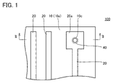
- FIG. 1 is a plan view of a flexible printed circuit board 100.
- FIG. FIG. 2 is a cross-sectional view along II-II in FIG.
- FIG. 3 is a process diagram of a method for manufacturing the flexible printed circuit board 100.
- FIG. FIG. 4 is a cross-sectional view of the flexible printed circuit board 100 after performing the sputtering process S21.
- FIG. 5 is a cross-sectional view of the flexible printed circuit board 100 after the through-hole forming step S22 is performed.
- FIG. 6 is a cross-sectional view of the flexible printed circuit board 100 after the resist layer forming step S23 is performed.
- FIG. 7 is a cross-sectional view of the flexible printed circuit board 100 after the electroplating step S24 is performed.
- FIG. 8 is a cross-sectional view of the flexible printed circuit board 100 during the electroplating step S24.
- FIG. 9 is a cross-sectional view of the flexible printed circuit board 100 after the resist removing step S25 is performed.
- FIG. 10 is a cross-sectional view of the flexible printed circuit board 100A.
- FIG. 11 is a cross-sectional view of the flexible printed circuit board 100A in the vicinity of the electroless plating layer 60.
- FIG. FIG. 12 is a cross-sectional view of the flexible printed circuit board 100 after the electroplating step S24 is performed when the inner diameter D is smaller than the thickness T1.
- FIG. 13 is a cross-sectional view of the flexible printed circuit board 100B.
- a through hole is formed in the base film, and a base film is formed on the inner wall surface of the through hole.
- a conductive layer is formed to connect the wiring arranged on the surface of the base film and the wiring arranged on the back surface of the base film.
- the inner wall surface of the through hole is subjected to a conductive treatment before forming the resist layer. Conductive treatment is performed by forming an electroless plated layer on the inner wall surface of the through hole.
- the present disclosure has been made in view of the problems of the prior art as described above. More specifically, the present disclosure provides a flexible printed circuit board capable of suppressing wiring undercuts.
- a flexible printed circuit board includes an insulating layer having a first surface and a second surface opposite to the first surface, and first wiring disposed on the first surface. , a second wiring disposed on the second surface, and a conductive layer.
- the first wiring has a first land.
- the second wiring has a second land.
- the first wiring has a first layer arranged on the first surface and a second layer arranged on the first layer.
- the second wiring has a third layer arranged on the second surface and a fourth layer arranged on the third layer.
- the first land and the second land overlap in plan view.
- a through hole is formed in the insulating layer so as to penetrate the insulating layer in the thickness direction and at least partially overlap the first land and the second land in a plan view.
- a conductive layer is arranged on the inner wall surface of the through hole so as to be connected to the first land and the second land.
- the second layer, the fourth layer and the conductive layer are electrolytic plating layers made of the same material.
- the thickness of the first land and the second land is 0.5 times or more the thickness of the insulating layer.
- the thickness of the first land and the second land may be 0.75 times or more the thickness of the insulating layer.
- the reliability of the conductive layer can be enhanced.
- palladium particles may be dispersed between the inner wall surface of the through hole and the conductive layer.
- the inner diameter of the through hole may be equal to or greater than the thickness of the insulating layer.
- the first layer may be a sputter layer.
- a method for manufacturing a flexible printed circuit board includes the steps of preparing an insulating layer and forming a first wiring having a first land and a second wiring having a second land.
- the insulating layer has a first surface and a second surface opposite the first surface.
- the insulating layer is formed with a through hole that penetrates the insulating layer in the thickness direction and at least partially overlaps the first land and the second land in a plan view.
- the steps of forming the first wiring and the second wiring include forming a first layer on the first surface, forming a first resist layer on the first layer, and exposing from the first resist layer.
- the step of forming the second layer and the step of forming the fourth layer are performed by electroplating.
- the conductive layer is formed on the inner wall surface of the through hole by growing the second layer and the fourth layer along the inner wall surface of the through hole. .
- the first resist layer and the second resist layer are removed after the second layer and the fourth layer are formed.
- the first layer underlying the removed first resist layer and the third layer underlying the removed second resist layer are etched away after the second and fourth layers are formed.
- the thickness of the first land and the second land is 0.5 times or more the thickness of the insulating layer.
- FIG. 1 is a plan view of the flexible printed circuit board 100.
- FIG. FIG. 2 is a cross-sectional view along II-II in FIG.
- the flexible printed circuit board 100 has an insulating layer 10 , first wirings 20 , second wirings 30 and a conductive layer 40 .
- the insulating layer 10 is made of a material having electrical insulation and flexibility. Specific examples of the material forming the insulating layer 10 include polyimide, polyethylene terephthalate, and fluororesin.
- the insulating layer 10 has a first surface 10a and a second surface 10b. The first surface 10a and the second surface 10b are end surfaces in the thickness direction of the insulating layer 10 . The second surface 10b is the opposite surface of the first surface 10a.
- the thickness of the insulating layer 10 is assumed to be a thickness T1.
- the thickness T1 is, for example, 5 ⁇ m or more and 100 ⁇ m or less.
- the first wiring 20 is arranged on the first surface 10a.
- the first wiring 20 has a first land 20a.
- the first land 20a is at the end of the first wiring 20, for example.
- the first land 20a has, for example, a rectangular shape in plan view.
- the thickness of the first land 20a is assumed to be thickness T2.
- the thickness T2 is at least 0.5 times the thickness T1.
- the thickness T2 may be 0.75 times or more the thickness T1.
- the thickness T2 may be 1.0 times or more the thickness T1.
- the thickness T2 may be less than or equal to 2.0 times the thickness T1.
- the thickness T2 may be 4.0 times or less than the thickness T1, or may be 6.0 times or less than the thickness T1.
- the thickness T2 may be less than 0.5 times the inner diameter D described below.
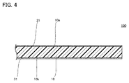
- the first wiring 20 has a first layer 21 and a second layer 22 .
- the first layer 21 is made of copper (Cu), for example.
- the first layer 21 is, for example, a sputter layer (a layer formed by sputtering).
- the second layer 22 is made of copper, for example.
- the second layer 22 is an electrolytic plated layer (a layer formed by electrolytic plating).
- the second layer 22 is arranged on the first layer 21 .
- the thickness of the first layer 21 is smaller than the thickness of the second layer 22 .
- the second wiring 30 is arranged on the second surface 10b.
- the second wiring 30 has a second land 30a.
- the second land 30a is at the end of the second wiring 30, for example.
- the second land 30a has, for example, a rectangular shape in plan view.
- the second land 30a overlaps the first land 20a in plan view.
- the first land 20a and the second land 30a may have the same shape and the same size in plan view.
- the first land 20a and the second land 30a may have different shapes or different sizes in plan view.
- the thickness of the second land 30a is assumed to be thickness T3.
- the thickness T3 is 0.5 times or more the thickness T1.
- the thickness T3 is at least 0.75 times the thickness T1.
- the thickness T3 may be 1.0 times or more the thickness T1.
- the thickness T3 may be less than or equal to 2.0 times the thickness T1.
- the thickness T3 may be 4.0 times or less than the thickness T1, or may be 6.0 times or less than the thickness T1.
- the thickness T3 may be less than 0.5 times the inner diameter D described later.
- the second wiring 30 has a third layer 31 and a fourth layer 32 .
- the third layer 31 is made of copper, for example.
- the third layer 31 is, for example, a sputter layer.
- the fourth layer 32 is made of copper, for example.
- the fourth layer 32 is an electrolytic plating layer. That is, the fourth layer 32 is an electrolytic plated layer made of the same material as the second layer 22 .
- the fourth layer 32 is arranged on the third layer 31 .
- the thickness of the third layer 31 is smaller than the thickness of the fourth layer 32 .
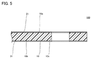
- a through hole 10 c is formed in the insulating layer 10 .
- the through hole 10c penetrates the insulating layer 10 along the thickness direction.
- the through hole 10c overlaps the first land 20a and the second land 30a in plan view.
- the through hole 10c may partially overlap the first land 20a and the second land 30a in plan view.
- An inner diameter D is the inner diameter of the through hole 10c.
- the inner diameter D is equal to or greater than the thickness T1.
- the conductive layer 40 is arranged on the inner wall surface of the through hole 10c.
- the conductive layer 40 is connected to the first land 20a and the second land 30a. Thereby, the first land 20a and the second land 30a are electrically connected to each other.
- the conductive layer 40 is made of copper, for example.
- the conductive layer 40 is an electrolytic plating layer. That is, the conductive layer 40 is an electrolytic plated layer made of the same material as the second layer 22 and the fourth layer 32 .
- the conductive layer 40 arranged on the inner wall surface of the through hole 10c may have a single-layer structure.
- FIG. 3 is a process diagram of a method for manufacturing the flexible printed circuit board 100.
- the method for manufacturing the flexible printed circuit board 100 includes a preparation step S1 and a wiring formation step S2.
- the wiring formation step S2 is performed after the preparation step S1.
- the wiring forming step S2 includes a sputtering step S21, a through hole forming step S22, a resist layer forming step S23, an electrolytic plating step S24, a resist removing step S25, and an etching step S26.
- the through-hole forming step S22 is performed after the sputtering step S21.
- the resist layer forming step S23 is performed after the through hole forming step S22.
- the electrolytic plating step S24 is performed after the resist layer forming step S23.
- the resist removing step S25 is performed after the electroplating step S24.
- the etching step S26 is performed after the resist removing step S25.
- FIG. 4 is a cross-sectional view of the flexible printed circuit board 100 after performing the sputtering step S21. As shown in FIG. 4, in the sputtering step S21, sputtering is performed to form the first layer 21 on the first surface 10a and to form the third layer 31 on the second surface 10b. .
- FIG. 5 is a cross-sectional view of the flexible printed circuit board 100 after the through-hole forming step S22 has been performed. As shown in FIG. 5, in the through-hole forming step S22, through-holes 10c are formed.
- the through hole 10c is formed by, for example, laser processing or machining using a drill or the like.
- FIG. 6 is a cross-sectional view of the flexible printed circuit board 100 after performing the resist layer forming step S23.
- a resist layer 50 is formed on the first layer 21 and the third layer 31 in the resist layer forming step S23.
- a photosensitive organic material forming the resist layer 50 is deposited.
- the photosensitive organic material forming the deposited resist layer 50 is exposed and developed. Thereby, a patterned resist layer 50 is formed on the first layer 21 and the third layer 31 .
- FIG. 7 is a cross-sectional view of the flexible printed circuit board 100 after the electroplating step S24 has been performed.
- the flexible printed circuit board 100 in the electrolytic plating step S24, the flexible printed circuit board 100 is immersed in a plating solution, and the first layer 21 and the third layer 31 are energized. Thereby, the second layer 22 is electroplated on the first layer 21 exposed from the resist layer 50 , and the fourth layer 32 is electroplated on the third layer 31 exposed from the resist layer 50 .
- FIG. 8 is a cross-sectional view of the flexible printed circuit board 100 during the electroplating step S24.
- the second layer 22 is formed into the through holes 10c during the electroplating step S24. It also grows along the inner wall surface in the direction from the first surface 10a to the second surface 10b.
- the fourth layer 32 also grows in the direction from the second surface 10b toward the first surface 10a along the inner wall surface of the through hole 10c during the electroplating step S24.
- the conductive layer 40 is formed by integrating the second layer 22 and the fourth layer 32 grown along the inner wall surface of the through hole 10c.
- FIG. 9 is a cross-sectional view of the flexible printed circuit board 100 after performing the resist removing step S25.
- the resist layer 50 is removed in the resist removing step S25.
- the etching step S26 the first layer 21 and the third layer 31 under the removed resist layer 50 are removed by etching. This etching is performed by wet etching or dry etching. As described above, the flexible printed circuit board 100 having the structure shown in FIGS. 1 and 2 is manufactured.
- FIG. 10 is a cross-sectional view of the flexible printed circuit board 100A.
- the flexible printed circuit board 100A further has an electroless plated layer 60.
- the electroless plating layer 60 is arranged between the first layer 21 and the second layer 22, between the third layer 31 and the fourth layer 32, and between the inner wall surface of the through hole 10c and the conductive layer 40.
- the flexible printed circuit board 100A is in common with the flexible printed circuit board 100.
- the electroless plated layer 60 is formed after the through-hole forming step S22 and before the resist layer forming step S23.
- FIG. 11 is a cross-sectional view of the flexible printed circuit board 100A in the vicinity of the electroless plating layer 60.
- FIG. Since it is necessary to remove the electroless plated layer 60 in addition to the first layer 21 (the third layer 31) in the etching step S26, the flexible printed circuit board 100A requires a longer time for the etching step S26. Moreover, in the flexible printed circuit board 100A, etching easily progresses at the interface between the first layer 21 (third layer 31) and the electroless plated layer 60 . Therefore, in the flexible printed circuit board 100A, as shown in FIG. 11, undercuts are likely to occur under the second layer 22 (fourth layer 32).
- the undercut of the first wiring 20 means that at least one of the first layer 21, the second layer 22 and the electroless plated layer 60 at the bottom of the first wiring 20 or at least one of the interface between these layers is It refers to a phenomenon in which the bottom of the first wiring 20 becomes concave due to excessive etching compared to the top of the first wiring 20 .
- the undercut of the second wiring 30 means at least one of the third layer 31, the fourth layer 32, and the electroless plated layer 60 at the bottom of the second wiring 30, or at least the interface between these layers. It refers to a phenomenon in which the bottom of the second wiring 30 becomes concave due to excessive etching of either of them compared to the top of the second wiring 30 .
- the flexible printed circuit board 100 since the electroless plating layer 60 is not formed, the time required for the etching step S26 is shortened and the interface between the first layer 21 and the electroless plating layer 60 does not exist. Therefore, according to the flexible printed circuit board 100, occurrence of undercut under the second layer 22 and the fourth layer 32 is suppressed.
- FIG. 12 is a cross-sectional view of the flexible printed circuit board 100 after the electroplating step S24 is performed when the inner diameter D is smaller than the thickness T1.
- the second layer 22 and the fourth layer 32 do not grow along the inner wall surface of the through hole 10c, and penetrate through. It may straddle the hole 10c.
- the second layer 22 and the fourth layer 32 are likely to grow along the inner wall surface of the through hole 10c, and the conductive layer 40 allows the first land 20a and the second land 30a to be separated from each other. It becomes easier to secure an electrical connection between the
- the peel strength of the conductive layer 40 on the inner wall surface of the through hole 10c can be increased.
- the thickness T2 and the thickness T3 are 2.0 times or less, 4.0 times or less, or 6.0 times or less the thickness T1
- the peel strength of the conductive layer 40 on the inner wall surface of the through hole 10c can be increased. can.
- the thickness T2 and the thickness T3 are less than 0.5 times the inner diameter D, the through hole 10c is partially filled with the conductive layer 40, thereby suppressing the generation of voids.
- Example 2 A heat shock test was performed on the flexible printed circuit board 100 in order to evaluate the reliability of the conductive layer 40 .
- thickness T1, thickness T2 and thickness T3 were varied.
- the inner diameter D was constant at 100 ⁇ m.
- one cycle consisted of changing the temperature within the range of -40°C to 130°C for 30 minutes, and this cycle was repeated 1000 times.
- the electrical resistance value between the first land 20a and the second land 30a was measured.
- electrical resistance values were measured for 1,000,000 locations of the conductive layer 40 for each sample.
- the results of the heat shock test were all C when the thickness T2 and the thickness T3 were less than 0.5 times the thickness T1.
- all the results of the heat shock test were B or more. Therefore, by satisfying the condition that the thickness T2 and the thickness T3 are 0.5 times or more the thickness T1, the conductive layer 40 is appropriately formed on the inner wall surface of the through hole 10c. It has been found that an electrical connection is made between the first land 20a and the second land 30a.
- a flexible printed circuit board 100 (referred to as “flexible printed circuit board 100B”) according to a modification will be described below.
- points different from the flexible printed circuit board 100 will be mainly described, and redundant description will not be repeated.
- FIG. 13 is a cross-sectional view of the flexible printed circuit board 100B.
- flexible printed circuit board 100B further has palladium particles 70 .
- Palladium particles 70 are dispersed between the inner wall surface of through hole 10 c and conductive layer 40 .
- the flexible printed circuit board 100A is common to the flexible printed circuit board 100.
- the palladium particles 70 are arranged on the inner wall surfaces of the through holes 10c after the through hole forming step S22 and before the resist layer forming step S23.
- the second layer 22 grows from the first surface 10a toward the second surface 10b along the inner wall surface of the through hole 10c, and the fourth layer 32 grows on the inner wall surface of the through hole 10c. Since the conductive layer 40 is formed by growing along the second surface 10b toward the first surface 10a side, the second layer 22 grown from the first surface 10a toward the second surface 10b side and the second layer 22 growing toward the second surface 10b side are formed. Voids may occur in the vicinity of the portion where the fourth layer 32 grown from the second surface 10b toward the first surface 10a contacts.
- the flexible printed circuit board 100B in addition to the growth of the second layer 22 from the first surface 10a toward the second surface 10b and the growth of the fourth layer 32 from the second surface 10b toward the first surface 10a, The growth of the electroplated layer on the inner wall surface of through-hole 10 c with palladium particles 70 as nuclei also contributes to the formation of conductive layer 40 . Therefore, according to the flexible printed circuit board 100B, the occurrence of voids as described above in the conductive layer 40 is suppressed.
Landscapes
- Engineering & Computer Science (AREA)
- Microelectronics & Electronic Packaging (AREA)
- Manufacturing & Machinery (AREA)
- Printing Elements For Providing Electric Connections Between Printed Circuits (AREA)
- Manufacturing Of Printed Wiring (AREA)
Priority Applications (3)
| Application Number | Priority Date | Filing Date | Title |
|---|---|---|---|
| CN202280007300.5A CN116530222A (zh) | 2021-04-22 | 2022-04-12 | 柔性印刷电路基板及柔性印刷电路基板的制造方法 |
| US18/036,816 US20230413451A1 (en) | 2021-04-22 | 2022-04-12 | Flexible printed circuit board and method of manufacturing flexible printed circuit board |
| JP2023516454A JP7544965B2 (ja) | 2021-04-22 | 2022-04-12 | フレキシブルプリント回路基板及びフレキシブルプリント回路基板の製造方法 |
Applications Claiming Priority (2)
| Application Number | Priority Date | Filing Date | Title |
|---|---|---|---|
| JP2021072660 | 2021-04-22 | ||
| JP2021-072660 | 2021-04-22 |
Publications (1)
| Publication Number | Publication Date |
|---|---|
| WO2022224866A1 true WO2022224866A1 (ja) | 2022-10-27 |
Family
ID=83722990
Family Applications (1)
| Application Number | Title | Priority Date | Filing Date |
|---|---|---|---|
| PCT/JP2022/017552 Ceased WO2022224866A1 (ja) | 2021-04-22 | 2022-04-12 | フレキシブルプリント回路基板及びフレキシブルプリント回路基板の製造方法 |
Country Status (4)
| Country | Link |
|---|---|
| US (1) | US20230413451A1 (https=) |
| JP (1) | JP7544965B2 (https=) |
| CN (1) | CN116530222A (https=) |
| WO (1) | WO2022224866A1 (https=) |
Cited By (1)
| Publication number | Priority date | Publication date | Assignee | Title |
|---|---|---|---|---|
| JP7680647B1 (ja) * | 2024-10-22 | 2025-05-20 | 住友電気工業株式会社 | プリント配線板 |
Citations (2)
| Publication number | Priority date | Publication date | Assignee | Title |
|---|---|---|---|---|
| CN102686052A (zh) * | 2011-03-16 | 2012-09-19 | 钒创科技股份有限公司 | 软性印刷电路板及其制造方法 |
| KR101555014B1 (ko) * | 2014-04-07 | 2015-09-22 | (주) 화인켐 | 미세배선용 인쇄회로기판 및 이의 제조방법 |
Family Cites Families (10)
| Publication number | Priority date | Publication date | Assignee | Title |
|---|---|---|---|---|
| US3099608A (en) * | 1959-12-30 | 1963-07-30 | Ibm | Method of electroplating on a dielectric base |
| US3506482A (en) * | 1967-04-25 | 1970-04-14 | Matsushita Electric Industrial Co Ltd | Method of making printed circuits |
| JPS5686964A (en) * | 1979-12-13 | 1981-07-15 | Kollmorgen Tech Corp | High resolving power screen printable resist |
| FR2759528B1 (fr) * | 1997-02-11 | 2006-12-22 | Thomson Csf | Procede de realisation de circuits imprimes a double epargne |
| BR0114436A (pt) * | 2000-10-06 | 2003-07-01 | Tanabe Seiyaku Co | Composto com anel de cinco elementos contendo nitrogênio alifático |
| US7317245B1 (en) * | 2006-04-07 | 2008-01-08 | Amkor Technology, Inc. | Method for manufacturing a semiconductor device substrate |
| JP6061470B2 (ja) * | 2012-01-20 | 2017-01-18 | 旭化成株式会社 | フレキシブル配線板 |
| JP6601814B2 (ja) * | 2014-05-21 | 2019-11-06 | 住友電工プリントサーキット株式会社 | プリント配線板及びプリント配線板の製造方法 |
| KR102014462B1 (ko) * | 2015-10-23 | 2019-08-26 | 주식회사 엘지화학 | 이차 전지용 카트리지 및 이를 포함하는 배터리 모듈 |
| JP6943681B2 (ja) * | 2017-08-24 | 2021-10-06 | 住友電気工業株式会社 | プリント配線板 |
-
2022
- 2022-04-12 WO PCT/JP2022/017552 patent/WO2022224866A1/ja not_active Ceased
- 2022-04-12 CN CN202280007300.5A patent/CN116530222A/zh active Pending
- 2022-04-12 US US18/036,816 patent/US20230413451A1/en active Pending
- 2022-04-12 JP JP2023516454A patent/JP7544965B2/ja active Active
Patent Citations (2)
| Publication number | Priority date | Publication date | Assignee | Title |
|---|---|---|---|---|
| CN102686052A (zh) * | 2011-03-16 | 2012-09-19 | 钒创科技股份有限公司 | 软性印刷电路板及其制造方法 |
| KR101555014B1 (ko) * | 2014-04-07 | 2015-09-22 | (주) 화인켐 | 미세배선용 인쇄회로기판 및 이의 제조방법 |
Cited By (1)
| Publication number | Priority date | Publication date | Assignee | Title |
|---|---|---|---|---|
| JP7680647B1 (ja) * | 2024-10-22 | 2025-05-20 | 住友電気工業株式会社 | プリント配線板 |
Also Published As
| Publication number | Publication date |
|---|---|
| JP7544965B2 (ja) | 2024-09-03 |
| CN116530222A (zh) | 2023-08-01 |
| US20230413451A1 (en) | 2023-12-21 |
| JPWO2022224866A1 (https=) | 2022-10-27 |
Similar Documents
| Publication | Publication Date | Title |
|---|---|---|
| US20080128288A1 (en) | Method of manufacturing a multi-layer wiring board using a metal member having a rough surface | |
| US20070246252A1 (en) | Manufacture of printed circuit boards with stubless plated through-holes | |
| KR101055501B1 (ko) | 인쇄회로기판 및 인쇄회로기판의 제조방법 | |
| JP2017504193A (ja) | 印刷回路基板用セグメントビアの形成方法 | |
| KR20060047598A (ko) | 배선 회로 기판 및 그 제조 방법 | |
| JP2002134864A (ja) | 配線基板及び配線基板の製造方法 | |
| WO2022224866A1 (ja) | フレキシブルプリント回路基板及びフレキシブルプリント回路基板の製造方法 | |
| JP2009099964A (ja) | 配線基板の製造方法 | |
| JP7294588B2 (ja) | 印刷回路基板の製造方法及びこれを用いて製造した印刷回路基板 | |
| CN107347231B (zh) | 线路基板的制作方法 | |
| JP2009295635A (ja) | プリント配線板 | |
| KR101102789B1 (ko) | 이종금속 종자층을 기반으로 하는 에스에이피 공법의 홀 도금처리 방법 | |
| KR20050046565A (ko) | 양면 배선 회로 기판 | |
| JP2002324968A (ja) | 配線基板の製造方法 | |
| TWI394246B (zh) | 封裝基板及其製法 | |
| JPS6336598A (ja) | 配線板の製造方法 | |
| KR101067074B1 (ko) | 인쇄회로기판 및 인쇄회로기판의 제조방법 | |
| KR20050017905A (ko) | 연성인쇄회로기판 제조방법 및 그에 의해 제조된연성회로기판 | |
| JP4160813B2 (ja) | 多層回路基板の製造法 | |
| TWI621379B (zh) | 電路板及其製造方法 | |
| KR101363076B1 (ko) | 인쇄회로기판 및 그 제조 방법 | |
| JPH03181195A (ja) | 配線基板の製造方法 | |
| JP2022189660A (ja) | プリント配線板 | |
| JP2026046879A (ja) | プリント配線板の製造方法 | |
| JP2005268593A (ja) | プリント配線板およびその製造方法 |
Legal Events
| Date | Code | Title | Description |
|---|---|---|---|
| 121 | Ep: the epo has been informed by wipo that ep was designated in this application |
Ref document number: 22791640 Country of ref document: EP Kind code of ref document: A1 |
|
| ENP | Entry into the national phase |
Ref document number: 2023516454 Country of ref document: JP Kind code of ref document: A |
|
| WWE | Wipo information: entry into national phase |
Ref document number: 202280007300.5 Country of ref document: CN |
|
| NENP | Non-entry into the national phase |
Ref country code: DE |
|
| 122 | Ep: pct application non-entry in european phase |
Ref document number: 22791640 Country of ref document: EP Kind code of ref document: A1 |