WO2022209950A1 - 高エネルギー線用レジスト組成物、高エネルギー線用レジスト組成物の製造方法、レジストパターン形成方法、及び半導体装置の製造方法 - Google Patents
高エネルギー線用レジスト組成物、高エネルギー線用レジスト組成物の製造方法、レジストパターン形成方法、及び半導体装置の製造方法 Download PDFInfo
- Publication number
- WO2022209950A1 WO2022209950A1 PCT/JP2022/012230 JP2022012230W WO2022209950A1 WO 2022209950 A1 WO2022209950 A1 WO 2022209950A1 JP 2022012230 W JP2022012230 W JP 2022012230W WO 2022209950 A1 WO2022209950 A1 WO 2022209950A1
- Authority
- WO
- WIPO (PCT)
- Prior art keywords
- resist composition
- energy ray
- group
- present disclosure
- resist
- Prior art date
- Legal status (The legal status is an assumption and is not a legal conclusion. Google has not performed a legal analysis and makes no representation as to the accuracy of the status listed.)
- Ceased
Links
Images


Classifications
-
- G—PHYSICS
- G03—PHOTOGRAPHY; CINEMATOGRAPHY; ANALOGOUS TECHNIQUES USING WAVES OTHER THAN OPTICAL WAVES; ELECTROGRAPHY; HOLOGRAPHY
- G03F—PHOTOMECHANICAL PRODUCTION OF TEXTURED OR PATTERNED SURFACES, e.g. FOR PRINTING, FOR PROCESSING OF SEMICONDUCTOR DEVICES; MATERIALS THEREFOR; ORIGINALS THEREFOR; APPARATUS SPECIALLY ADAPTED THEREFOR
- G03F7/00—Photomechanical, e.g. photolithographic, production of textured or patterned surfaces, e.g. printing surfaces; Materials therefor, e.g. comprising photoresists; Apparatus specially adapted therefor
- G03F7/004—Photosensitive materials
- G03F7/0042—Photosensitive materials with inorganic or organometallic light-sensitive compounds not otherwise provided for, e.g. inorganic resists
-
- G—PHYSICS
- G03—PHOTOGRAPHY; CINEMATOGRAPHY; ANALOGOUS TECHNIQUES USING WAVES OTHER THAN OPTICAL WAVES; ELECTROGRAPHY; HOLOGRAPHY
- G03F—PHOTOMECHANICAL PRODUCTION OF TEXTURED OR PATTERNED SURFACES, e.g. FOR PRINTING, FOR PROCESSING OF SEMICONDUCTOR DEVICES; MATERIALS THEREFOR; ORIGINALS THEREFOR; APPARATUS SPECIALLY ADAPTED THEREFOR
- G03F7/00—Photomechanical, e.g. photolithographic, production of textured or patterned surfaces, e.g. printing surfaces; Materials therefor, e.g. comprising photoresists; Apparatus specially adapted therefor
- G03F7/004—Photosensitive materials
-
- G—PHYSICS
- G03—PHOTOGRAPHY; CINEMATOGRAPHY; ANALOGOUS TECHNIQUES USING WAVES OTHER THAN OPTICAL WAVES; ELECTROGRAPHY; HOLOGRAPHY
- G03F—PHOTOMECHANICAL PRODUCTION OF TEXTURED OR PATTERNED SURFACES, e.g. FOR PRINTING, FOR PROCESSING OF SEMICONDUCTOR DEVICES; MATERIALS THEREFOR; ORIGINALS THEREFOR; APPARATUS SPECIALLY ADAPTED THEREFOR
- G03F7/00—Photomechanical, e.g. photolithographic, production of textured or patterned surfaces, e.g. printing surfaces; Materials therefor, e.g. comprising photoresists; Apparatus specially adapted therefor
- G03F7/20—Exposure; Apparatus therefor
- G03F7/2002—Exposure; Apparatus therefor with visible light or UV light, through an original having an opaque pattern on a transparent support, e.g. film printing, projection printing; by reflection of visible or UV light from an original such as a printed image
- G03F7/2004—Exposure; Apparatus therefor with visible light or UV light, through an original having an opaque pattern on a transparent support, e.g. film printing, projection printing; by reflection of visible or UV light from an original such as a printed image characterised by the use of a particular light source, e.g. fluorescent lamps or deep UV light
Definitions
- the present invention relates to a resist composition for high energy rays. Specifically, it relates to a resist composition for extreme ultraviolet light and/or a resist composition for electron beams. The present invention also relates to a method for producing a resist composition for high-energy radiation, a method for forming a resist pattern, and a method for producing a semiconductor device.
- Non-Patent Document 1 discloses EUV lithography using a high-energy ray resist composition containing a compound containing tin-oxocage and OH ⁇ , an acetate anion, a malonate anion, or a tosylate anion.
- an object of the present disclosure is to provide a resist composition for high-energy radiation that can form a resist film (resist pattern) with good film quality and substrate adhesion when used in lithography using high-energy radiation. do.
- the composition of the present disclosure is a high-energy ray resist composition containing an anion represented by the following general formula (1) and a cluster containing a metal.
- R 1 represents an organic group having 1 to 30 carbon atoms
- R 2 and R 3 each independently represent a fluorine atom, a hydrogen atom, or a represents an organic group.
- the high-energy beam resist composition of the present disclosure in high-energy beam lithography, it is possible to create a good pattern in which the occurrence of defects is suppressed.
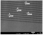
- 1 is an SEM image of a pattern formed by electron beam lithography using a resist composition containing tin oxocluster hydroxide (Compound A).
- the concentration of compound A in the resist composition is 20 mg/ml
- the magnification of the SEM image is 10,000
- the pattern has a pitch of 600 nm and a pattern of 200 nm
- the output of the high energy beam is 2000 ⁇ C/cm 2 .
- 1 is an SEM image of a pattern formed by electron beam lithography using a resist composition (high-energy ray resist composition (1) of the present disclosure) containing tin oxocluster vinyl trifluoroborate (compound 1).
- the concentration of compound 1 in the resist composition was 20 mg/ml, the magnification of the SEM image was 10,000 times, the pattern had a pitch of 600 nm and a pattern of 200 nm, and the output of the high energy beam was 2000 ⁇ C/cm 2 .
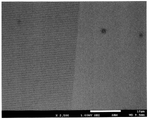
- 1 is an SEM image of a pattern formed by electron beam lithography using a resist composition containing tin oxocluster hydroxide (Compound A).
- the concentration of compound A in the resist composition was 20 mg/ml, the magnification of the SEM image was 2,500 times, the pattern had a pitch of 600 nm and a pattern of 200 nm, and the output of the high energy beam was 2000 ⁇ C/cm 2 .
- 1 is an SEM image of a pattern formed by electron beam lithography using a resist composition (high-energy ray resist composition (1) of the present disclosure) containing tin oxocluster vinyl trifluoroborate (compound 1).
- the concentration of compound 1 in the resist composition was 20 mg/ml, the magnification of the SEM image was 2,500 times, the pattern had a pitch of 600 nm and a pattern of 200 nm, and the output of the high energy beam was 2000 ⁇ C/cm 2 .
- 1 is an SEM image of a pattern formed by electron beam lithography using a resist composition (high-energy ray resist composition (1) of the present disclosure) containing tin oxocluster vinyl trifluoroborate (compound 1).
- the concentration of compound 1 in the resist composition is 20 mg/ml, the magnification of the SEM image is 100,000 times, the pattern has a pitch of 60 nm and a pattern of 20 nm, and the output of the high energy beam is 240 ⁇ C/cm 2 .
- 1 is a NMR chart of 119 Sn of tin oxocluster vinyl trifluoroborate (Compound 1).
- the high-energy ray resist composition of the present disclosure contains a fluorinated borate anion and a metal-containing cluster.
- a compound containing the above fluorinated borate anion and a metal-containing cluster is hereinafter also referred to as a “compound of the present disclosure”.
- high-energy radiation means ionizing radiation or non-ionizing radiation with a wavelength of 13.5 nm or less, ionizing radiation non-particle radiation (electromagnetic waves) such as X-rays, wavelengths from 1 to Light rays (non-ionizing radiation) such as 13.5 nm (especially 13.5 nm) EUV, or ionizing radiation particle beams such as electron beams are exemplified.
- the high-energy ray resist composition of the present disclosure and the compound of the present disclosure contain a fluorinated borate anion (hereinafter also referred to as "fluorinated borate anion of the present disclosure").
- the fluorinated borate anion of the present disclosure may be an anion having at least one BF bond, but is preferably an anion having a structure represented by the following general formula (1).
- R 1 represents an organic group having 1 to 30 carbon atoms
- R 2 and R 3 each independently represent a fluorine atom, a hydrogen atom, or a represents an organic group.
- examples of the organic group represented by R 1 include an alkyl group, an alkenyl group, an aryl group, a heterocyclic group, a group in which a hydrocarbon group is bonded to a silicon atom, a cyano group, an acyl group, and the like. are exemplified, and these may have substituents.
- the hydrocarbon groups bonded to silicon atoms include aliphatic hydrocarbon groups and aromatic hydrocarbon groups.
- Aliphatic hydrocarbon groups may be saturated or unsaturated and may be linear or alicyclic.
- the hydrocarbon group bonded to the silicon atom is preferably an aliphatic hydrocarbon group having 1 or more and 10 or less carbon atoms, an aromatic hydrocarbon group having 6 or more and 15 or less carbon atoms, and a saturated hydrocarbon group having 1 or more and 6 or less carbon atoms.
- a chain aliphatic hydrocarbon group and an aromatic hydrocarbon group having 6 or more and 12 or less carbon atoms are more preferable.
- Examples of the substituents that the organic group represented by R 1 may have include alkyl groups, alkenyl groups, aryl groups, heterocyclic groups, cyano groups, acyl groups, amino groups, alkoxy groups, and aryloxy groups (aryl oxy group), hydroxyl group, carboxy group, sulfonic acid group, sulfate ester group, phosphoric acid group, halogen atom and the like.
- the organic group represented by R 1 may have one or more substituents, and may have one or more substituents.
- the number of carbon atoms in the organic group represented by R 1 is preferably 1 or more, more preferably 2 or more, preferably 30 or less, more preferably 20 or less, and 10 or less. is more preferable.
- the organic group represented by R 1 has a substituent, the number of carbon atoms including the substituent is preferably within the above range.
- Examples of the organic group represented by R 1 in the general formula (1) include methyl group, n-propyl group, iso-propyl group, n-butyl group, sec-butyl group, iso-butyl group, tert -butyl group, n-hexyl group, n-octyl group, n-decyl group, cyclopentyl group, cyclohexyl group, benzyl group, p-methoxybenzyl group, phenylethyl group, etc., unsubstituted or substituted alkyl group; unsubstituted or substituted alkenyl groups such as vinyl group, allyl group, crotyl group, cinnamyl group; phenyl group, biphenyl group, naphthyl group, anthracenyl group, toluyl group, p-tert-butylphenyl group, m-methoxy unsubstitute
- the organic group represented by R 1 is preferably an unsubstituted or substituted alkyl group, an unsubstituted or substituted alkenyl group, and an unsubstituted or substituted aryl group.
- examples of the substituent that the organic group represented by R 1 may have include the groups exemplified as the organic group represented by R 1 above.
- substituents that the organic group represented by R 1 may have include, in addition to the groups exemplified as the organic group represented by R 1 , halogen atoms such as iodine, bromine, and fluorine.
- alkoxy group having unsubstituted or substituted group such as methoxy group and ethoxy group; aryloxy group having unsubstituted or substituted group such as phenoxy group; unsubstituted amino group; monomethylamino group, dimethylamino group, monodiethylamino group, diethylamino substituted amino groups such as groups; acid group-containing groups such as carboxy groups, sulfonic acid groups, sulfate ester groups, phosphoric acid groups, and salts thereof; sulfur-containing groups such as thiol groups and methylsulfanyl groups;
- the substituent that the organic group represented by R 1 may have is preferably a halogen atom, an unsubstituted or substituted alkoxy group, more preferably a halogen atom or an unsubstituted alkoxy group.
- the organic group represented by R 1 when it has a substituent, it may have one, two or more, or one type. , may have two or more kinds.
- R 2 and/or R 3 are organic groups having 1 to 5 carbon atoms are the above examples and preferred forms of the organic groups represented by R 1 . It is the same as that which is an organic group of 1 or more and 5 or less.
- the organic group represented by R 2 and/or R 3 may have a substituent, and examples and preferred forms of the substituent are Examples of optional substituents and preferred forms are the same.
- the number of carbon atoms including the substituent is preferably in the range of 1 to 5.
- At least one of R 2 and R 3 is preferably a fluorine atom, more preferably both R 2 and R 3 are fluorine atoms.
- the high-energy ray resist composition of the present disclosure and the compound of the present disclosure contain clusters containing metal (hereinafter also referred to as “metal clusters of the present disclosure”).
- the metal cluster of the present disclosure preferably contains a metal sensitive to high-energy rays, and more preferably contains at least one selected from Sn, Hf, Zr, Co, Pt, Pd, and Zn. Also, the metal is preferably contained as a constituent element of the cluster.
- the absorption cross-section of carbon to one or more types of ionizing radiation of 13.5 nm or less or non-ionizing radiation (especially EUV of 13.5 nm) is 1.5 nm. It means 2 times or more, preferably 2 times or more, more preferably 4 times or more, and still more preferably 8 times or more.
- the absorption cross-section of carbon is, for example, 3.5 ⁇ 10 5 cm 2 /mol when the wavelength is 13.5 nm (92 eV), and 7.7 ⁇ 10 cm 2 /mol when the wavelength is 6.75 nm (183 eV). 4 cm 2 /mol.
- a cluster containing a metal is a metal compound in which a plurality of metal atoms are directly or indirectly linked by a ligand, and may be a compound with a cage structure.
- the metal-comprising clusters of the present disclosure may optionally include ligands such as aqua ligands, hydroxo ligands, oxo ligands, peroxo ligands, thiolato ligands, sulfide ligands, fluoro one or more selected from ligands, chloro ligands, iodo ligands, hydride ligands, cyanato ligands, azide ligands, carboxylate ligands, oxalato ligands, etc.
- ligands such as aqua ligands, hydroxo ligands, oxo ligands, peroxo ligands, thiolato ligands, sulfide ligand
- the metal cluster of the present disclosure preferably contains one or two selected from oxo ligands and peroxo ligands, and a plurality of metal atoms indirectly by oxo ligands and / or peroxo ligands More preferably, they are connected. For example, when two or more metal atoms are linked via an oxo ligand, a structure such as MOM, MO(-M)-M (where M represents a metal atom) will include. Also, when two metal atoms are linked via a peroxo ligand, it includes the structure MOM (where M represents a metal atom).
- the metal clusters of the present disclosure are preferably metal oxide clusters.
- the metal cluster of the present disclosure preferably contains 2 or more metal atoms in one molecule, preferably 30 or less, more preferably 20 or less, and even more preferably 10 or less. Within the above range, the sensitivity in lithography using high-energy rays tends to be improved.
- the metal clusters of the present disclosure are preferably divalent cations. Specific examples of metal clusters of the present disclosure include tin oxo clusters, tin hydroxo clusters, Hf oxo clusters, Zr oxo clusters, and the like.
- the metal cluster of the present disclosure preferably has an organic group bonded to some or all of the metal atoms.
- the organic group that binds to the metal atom include the same organic groups as the organic group represented by R 1 in the general formula (1). More than one species of organic groups are preferred.
- the above alkyl group and alkenyl group may be linear, branched or cyclic.
- the organic group bonded to the metal atom is preferably an organic group having 1 or more and 30 or less carbon atoms, and the organic group may have one or more substituents.
- Preferred forms of the organic group that binds to the metal atom are the same as those of R 1 in the general formula (1) unless otherwise specified.
- the organic group that binds to the metal atom is particularly preferably an alkyl group, an alkenyl group or an aryl group having 1 to 20 carbon atoms, more preferably an alkyl group having 1 to 20 carbon atoms.
- An alkyl group of 1 or more and 10 or less is more preferable.
- the high-energy ray resist composition of the present disclosure may contain optional components other than the fluorinated borate anion of the present disclosure and the cluster containing the metal of the present disclosure.
- the high-energy ray resist composition of the present disclosure may contain an organic solvent.
- organic solvents examples include alcohols such as ethanol, isopropanol and 1-butanol; polyhydric alcohols such as ethylene glycol, diethylene glycol, propylene glycol and dipropylene glycol; acetone, methyl ethyl ketone, cyclohexanone, methyl-n-amyl ketone, methyl Ketones such as isoamyl ketone and 2-heptanone; ethyl acetate, propyl acetate, butyl acetate, methyl lactate, ethyl lactate, methyl pyruvate, ethyl pyruvate, methyl methoxypropionate, ethyl methoxypropionate, methyl ethoxypropionate, ethoxy Esters such as ethyl propionate and propylene glycol monomethyl ether acetate; anisole, ethylbenzyl ether, cresyl methyl ether, dipheny
- the ratio of the boron atom to the metal contained in the resist composition for high-energy radiation of the present disclosure is preferably 1 to 1 ⁇ 10 5 mol, more preferably 1 to 1000 mol, of the metal per 1 mol of the boron atom. and more preferably 1 to 20 mol. Within the above range, the film quality of the resist film tends to be improved.
- the metal is preferably at least one selected from Sn, Hf, Zr, Co, Pt, Pd and Zn.
- the ratio of the fluorinated borate anions of the present disclosure to the metal clusters of the present disclosure contained in the resist composition for high energy rays of the present disclosure is 0.001 to 5 metal clusters per 1 mol of the fluorinated borate anions. It is preferably ⁇ 10 4 mol, more preferably 0.01 to 100 mol, even more preferably 0.1 to 10 mol. Within the above range, the film quality of the resist film tends to be improved.
- the high-energy ray resist composition of the present disclosure preferably contains 1 ppm or more of boron atoms, more preferably 10 ppm or more, and even more preferably 100 ppm or more. Within the above range, the film quality of the resist film tends to be improved.
- ppm means a value calculated in terms of mass (for example, 10,000 ppm corresponds to 1% by mass).
- the high-energy ray resist composition of the present disclosure preferably contains 1 ppm or more of metal, more preferably 10 ppm or more, and even more preferably 100 ppm or more.
- the metal content in the high-energy ray resist composition of the present disclosure is preferably 60% by mass or less, more preferably 50% by mass or less, and even more preferably 40% by mass or less. Within the above range, the film quality of the resist film tends to be improved.
- the metal is preferably at least one selected from Sn, Hf, Zr, Co, Pt, Pd and Zn.
- the boron atom content and metal content can usually be analyzed by, for example, ICP, ICP-AES, or ICP-MS.
- the content of the organic solvent in the high-energy ray resist composition of the present disclosure is not particularly limited, and may be set as appropriate according to, for example, the coating film thickness. It is preferably 50% by mass or more, more preferably 80% by mass or more, and even more preferably 100% by mass or more relative to the total solid content of 100% by mass. In addition, it is preferably 1000% by mass or less, more preferably 800% by mass or less, and 500% by mass or less with respect to 100% by mass of the total solid content of the high-energy ray resist composition of the present disclosure. is more preferred. Within the above range, the film quality of the resist film tends to be improved.
- the total solid content of the resist composition for high-energy radiation refers to the total amount of the resist composition for high-energy radiation excluding the content of the solvent. The total solid content can be measured by known analysis means such as liquid chromatography or gas chromatography.
- the high-energy ray resist composition of the present disclosure or the compound of the present disclosure includes a step of mixing a metal-containing cluster and a fluorinated borate salt (hereinafter also referred to as a “mixing step”), and can be produced. preferable.
- the mixing step it is preferable to salt-exchange the anion contained in the metal-containing cluster and the fluorinated borate anion contained in the salt of the fluorinated borate.
- a solvent can be used in the mixing step. The type and amount of solvent to be used may be appropriately selected.
- the method for producing the high-energy ray resist composition of the present disclosure or the compound of the present disclosure preferably includes a purification step.
- a purification step for example, after the mixing step, distilling off the solvent and washing with water or an organic solvent are exemplified.
- the method for producing the high-energy ray resist composition of the present disclosure or the compound of the present disclosure preferably includes a solvent addition step.
- a solvent for example, it is preferable to add a solvent to the high-energy ray resist composition of the present disclosure or the compound of the present disclosure after the purification step to dissolve or disperse it.
- the metal-containing clusters used for producing the high-energy ray resist composition of the present disclosure or the compound of the present disclosure may be produced by a known method.
- the method of preparation by reacting below is preferred.
- M A is preferably a metal sensitive to high-energy rays, and the preferred form of R A is the same as R 1 in the general formula (1).
- M A is more preferably one selected from Sn, Hf, Zr, Co, Pt, Pd, and Zn
- R A is an alkyl group having 1 to 20 carbon atoms, an alkenyl group, or An aryl group is more preferred, an alkyl group having 1 to 20 carbon atoms is even more preferred, and an alkyl group having 1 to 10 carbon atoms is even more preferred.
- the acid catalyst may be either an organic acid or an inorganic acid.
- inorganic acids such as hydrochloric acid, sulfuric acid and phosphoric acid; p-toluenesulfonic acid, methanesulfonic acid, trifluoromethanesulfonic acid; and the like can be used.
- the fluorinated borate salt used in the production of the high-energy ray resist composition of the present disclosure or the compound of the present disclosure may also be produced by a known method, but the method of synthesizing from boronic acid is simple and preferred.
- Vedejs, E.; ; Chapman, R.; W. Fields, S.; C. Lin, S.; Schrimpf, M.; R. et al. Org. Chem. 1995, 60, 3020. can be easily synthesized from any boronic acid according to the synthesis method described in .
- the pattern forming method of the present disclosure comprises the steps (i) of applying the high-energy ray resist composition of the present disclosure, the step (ii) of drying the coating film of the high-energy ray resist composition, and The method includes a step (iii) of exposing the coating film of the resist composition to high-energy radiation, and a step (iv) of developing the film of the high-energy radiation resist composition.
- the resist pattern forming method of the present disclosure includes the step of applying the high-energy ray resist composition of the present disclosure (step (i)).
- step (i) By applying the high-energy ray resist composition of the present disclosure, a coating film of the high-energy ray resist composition of the present disclosure is formed.
- the method of applying the high-energy ray resist composition of the present disclosure is not particularly limited.
- the resist film can be formed using any coating method, the spin coating method is preferable from the viewpoint that a uniform thin film can be formed.
- the high-energy ray resist composition of the present disclosure is applied, for example, to a substrate or the like, but the substrate is not particularly limited and may have any size and dimension. GaAs, AlGaAs and the like are exemplified. Further, the substrate on which the resist film is formed may have a thin film processed into a desired pattern by dry etching or the like. insulating thin films such as films, metal thin films, Si oxide films, Si nitride films, and Si oxynitride films; An organic film may be further formed on the thin film.
- the high-energy ray resist composition of the present disclosure may be used to form an upper layer resist film in a multilayer resist structure.
- the coating amount of the resist composition for high-energy radiation of the present disclosure in step (i) can be appropriately adjusted, for example, so that the resist film has a film thickness described below.
- the method for forming a resist pattern of the present disclosure includes a step of drying a coating film of a resist composition for high-energy radiation (step (ii)).
- a coating film of the high-energy ray resist composition with a reduced solvent content is formed.
- Step (ii) is usually performed after step (i).
- the method for drying the coating film of the high-energy ray resist composition of the present disclosure is not particularly limited.
- the heating temperature is preferably 70° C. or higher, more preferably 80° C. or higher, still more preferably 90° C.
- Step (ii) may be carried out under reduced pressure, normal pressure or increased pressure, and may be carried out in an inert atmosphere.
- step (ii) it is preferable to carry out the coating film after drying (resist film after drying) so that the residual amount of the solvent is as small as possible.
- the coating film after drying has a solvent content of 1000 ppm or less.
- the resist pattern forming method of the present disclosure includes a step of exposing a coating film of a resist composition for high energy rays to high energy rays (step (iii)).
- a coating film is formed in which the exposed or unexposed portions are cured.
- Step (iii) is usually performed after step (ii).
- the method of exposing the coating film of the high-energy ray resist composition of the present disclosure to high-energy rays is not particularly limited. preferably done. Preferred forms of high-energy radiation are as described above.
- the exposure source used for exposure includes an EUV exposure source (LPP) that extracts EUV light from plasma generated by irradiating a target such as tin, its compound, or xenon with a laser beam, and the vicinity of an electrode made of tungsten, silicon carbide, or the like.
- An EUV exposure source (DPP) that extracts EUV light from a plasma generated by high-voltage discharge in which tin, its compounds, and xenon are present, EUV light from plasma generated by irradiating a target with laser light and discharging
- An EUV exposure source that extracts EUV light, an EUV exposure source that extracts EUV light from a radiation light source, an electron beam irradiation source, or the like is used.
- a reflective or transmissive filter may be used to extract high-energy radiation from a high-energy light source.
- the output of the high-energy radiation is preferably 0.5 mJ/cm 2 or more, and is preferably 1 mJ/cm 2 for non-ionizing radiation such as X-rays and non-ionizing radiation such as EUV light. more preferably at 2 mJ/cm 2 or more, more preferably at 500 mJ/cm 2 or less, more preferably 200 mJ/cm 2 or less, more preferably 100 mJ/cm 2 or less. is more preferred.
- Ionizing particle beams such as electron beams are preferably carried out at 10 ⁇ C/cm 2 or more, more preferably 20 ⁇ C/cm 2 or more, even more preferably 50 ⁇ C/cm 2 or more, and 10000 ⁇ C/cm 2 or less. It is preferably carried out at 5000 ⁇ C/cm 2 or less, more preferably 2500 ⁇ C/cm 2 or less.
- the resist pattern forming method of the present disclosure includes a step of developing the film of the high-energy ray resist composition of the present disclosure (step (iv)).
- a resist pattern can be formed by the development treatment.
- Step (iv) is usually performed after step (iii).
- the film (resist film) of the high-energy ray resist composition of the present disclosure is optionally developed using water, alkaline water, an organic solvent, or a mixture thereof.
- the solvent that can be used as the developer include the above organic solvents.
- Suitable organic solvents include alcohols such as 4-methyl-2-pentanol, 1-butanol, isopropanol, 1-propanol, and methanol; esters such as ethyl lactate; ethers such as tetrahydrofuran, dioxane, and anisole. ; amines such as tetramethylammonium hydroxide; and the like.
- the developer is optional, it may contain viscosity modifiers, solubilizing aids, surfactants, etc., if desired.
- the development time is preferably 10 seconds or longer, more preferably 20 seconds or longer, still more preferably 30 seconds or longer, preferably 300 seconds or shorter, more preferably 200 seconds or shorter, and even more preferably 100 seconds or shorter.
- the development method is not particularly limited, and examples thereof include an immersion method, a puddle method, and a spray method.
- the thickness of the resist film after development is preferably 10 nm or more, more preferably 20 nm or more, further preferably 30 nm or more, and 100 nm or less. is preferred, 80 nm or less is more preferred, and 60 nm or less is even more preferred. Also, the film thickness may be determined according to the minimum processing dimension of the desired pattern. Within the above range, the film quality of the resist film and the dimensional stability of the resist pattern tend to improve.
- the pattern formation method of the present disclosure may include arbitrary steps in addition to the steps (i), (ii), (iii), and (iv) described above.
- the optional step is exemplified by the step of baking the resist film after exposure to the high-energy rays (step (v)).
- step (v) is optional, but usually performed after step (iii).
- the heating temperature is preferably 70° C. or higher, more preferably 90° C. or higher, still more preferably 110° C. or higher, preferably 300° C. or lower, more preferably 250° C. or lower, and still more preferably 200° C. or lower. Heating may be performed under two or more different conditions.
- the heating time is preferably 10 seconds or longer, more preferably 30 seconds or longer, still more preferably 60 seconds or longer, preferably 300 seconds or shorter, more preferably 150 seconds or shorter, and even more preferably 120 seconds or shorter.
- the line width of the resist pattern is preferably, for example, 500 nm or less, more preferably 400 nm or less, and even more preferably 300 nm or less, from the viewpoint of miniaturization of the semiconductor device.
- a resist film having excellent film quality (pattern clarity) and substrate adhesion (developer resistance) can be formed. It is possible to form a good pattern in which the generation of defects is suppressed and the residual film in unnecessary portions is also suppressed.
- the method for manufacturing a semiconductor device of the present disclosure includes the step (i-b) of applying the high-energy ray resist composition of the present disclosure onto a substrate, and drying the coating film of the high-energy ray resist composition to obtain a resist.
- step (i-b), step (ii-b), step (iii-b), and step (iv-b) are respectively the above step (i), step (ii), step (iii), and step (iv) in the same form and preferred form.
- the method of manufacturing a semiconductor device according to the present disclosure may include arbitrary steps in addition to the steps described above. Examples of optional steps include the steps exemplified in the pattern formation method of the present disclosure.
- the high-energy ray resist composition of the present disclosure can be used for manufacturing semiconductor devices, manufacturing masks for semiconductor manufacturing devices, and the like.
- a resist film (resist pattern) formed using the resist composition for high-energy radiation of the present disclosure has good substrate adhesion (developer resistance). Specifically, it is preferable that the resist film is not peeled off by development. Moreover, the resist film (resist pattern) formed using the resist composition for high-energy radiation of the present disclosure has good film quality. Specifically, it is preferable that the resist pattern is clear without joining or disappearing.
- 1,4-Dioxane was added to the resulting solid, and the resulting solid was purified by recrystallization, and then filtered to obtain 14 g of the desired tin oxocluster p-toluenesulfonate.
- Example 9 400 mg of tin oxocluster hydroxide (compound A) and 98.4 mg of potassium (4-t-butylphenyl)trifluoroborate were added to a 100 mL round-bottom flask, 10 mL of tetrahydrofuran was added thereto, and the mixture was stirred at room temperature for 30 minutes. Then, the solvent was distilled off, and the resulting solid was washed with water and acetonitrile and dried to obtain 370 mg of tin oxocluster (4-t-butylphenyl)trifluoroborate (compound 7).
- Silicon wafers were cut into squares of approximately 1.5 cm and ultrasonically cleaned in isopropanol for 10 minutes. Moreover, it was made to boil for 3 minutes in isopropanol as it was. After that, the silicon wafer was taken out from the isopropanol, dried by blowing nitrogen, and UV ozone cleaning was performed for 2 minutes. Next, the silicon wafer was placed on a spin coater, 150 ⁇ L of hexamethyldisilazane was dropped, rotated at 4000 rpm for 35 seconds, and then baked on a hot plate at 150° C. for 1 minute to complete the surface treatment. .
- ⁇ Film formation on silicon wafer> As a reference, a 20 mg/mL 1-butanol solution of tin oxocluster hydroxide (compound A) was prepared (comparative resist composition). A 20 mg/mL 1-butanol solution of tin oxocluster vinyl trifluoroborate (compound 1) was also prepared (high-energy ray resist composition (1) of the present disclosure). The surface-treated silicon wafer was placed on a spin coater, each solution prepared was dropped, rotated at 1500 rpm for 45 seconds, and then baked on a hot plate at 90°C for 1 minute to complete the surface film formation. .
- the formed silicon wafer was set in an ultra-high-definition electron beam lithography apparatus (Elionix: ELS-100T), and lithography was performed while changing the output from 240 ⁇ C/cm 2 to 2000 ⁇ C/cm 2 .
- FIG. 2 is an SEM image at 10,000 times of a pattern formed by electron beam lithography (high energy beam output: 2000 ⁇ C/cm 2 ) using a resist composition containing tin oxocluster vinyl trifluoroborate (compound 1).
- an SEM image at 2,500 times is shown in FIG.
- FIGS. 1 and 2 show that the composition containing tin oxocluster vinyl trifluoroborate (Compound 1) is superior to tin oxocluster vinyl trifluoroborate (Compound A). It can be seen that the resist pattern obtained by using the film has fewer defects, and the film quality is good and the definition is high (the pattern is clear). Further, as shown in FIG. 5, by using the high-energy ray resist composition (1) of the present disclosure containing tin oxocluster vinyl trifluoroborate (compound 1), a pattern of about 20 nm can be drawn. , 240 ⁇ C/cm 2 , it can be confirmed that the negative type is reversed and the positive type is acting.
- the resist composition for high-energy radiation of the present disclosure can form a clear resist pattern in lithography using high-energy radiation, and can form a resist film having good film quality and substrate adhesion. became.
Landscapes
- Physics & Mathematics (AREA)
- General Physics & Mathematics (AREA)
- Chemical & Material Sciences (AREA)
- Organic Chemistry (AREA)
- Materials For Photolithography (AREA)
- Exposure And Positioning Against Photoresist Photosensitive Materials (AREA)
Priority Applications (2)
| Application Number | Priority Date | Filing Date | Title |
|---|---|---|---|
| KR1020237037503A KR102861297B1 (ko) | 2021-03-31 | 2022-03-17 | 고에너지선용 레지스트 조성물, 고에너지선용 레지스트 조성물의 제조 방법, 레지스트 패턴 형성 방법 및 반도체 장치의 제조 방법 |
| JP2023510936A JP7634650B2 (ja) | 2021-03-31 | 2022-03-17 | 高エネルギー線用レジスト組成物、高エネルギー線用レジスト組成物の製造方法、レジストパターン形成方法、及び半導体装置の製造方法 |
Applications Claiming Priority (2)
| Application Number | Priority Date | Filing Date | Title |
|---|---|---|---|
| JP2021059689 | 2021-03-31 | ||
| JP2021-059689 | 2021-03-31 |
Publications (1)
| Publication Number | Publication Date |
|---|---|
| WO2022209950A1 true WO2022209950A1 (ja) | 2022-10-06 |
Family
ID=83459160
Family Applications (1)
| Application Number | Title | Priority Date | Filing Date |
|---|---|---|---|
| PCT/JP2022/012230 Ceased WO2022209950A1 (ja) | 2021-03-31 | 2022-03-17 | 高エネルギー線用レジスト組成物、高エネルギー線用レジスト組成物の製造方法、レジストパターン形成方法、及び半導体装置の製造方法 |
Country Status (4)
| Country | Link |
|---|---|
| JP (1) | JP7634650B2 (https=) |
| KR (1) | KR102861297B1 (https=) |
| TW (1) | TWI877468B (https=) |
| WO (1) | WO2022209950A1 (https=) |
Cited By (3)
| Publication number | Priority date | Publication date | Assignee | Title |
|---|---|---|---|---|
| JP2023013561A (ja) * | 2021-07-16 | 2023-01-26 | 三星電子株式会社 | イオン性塩および感放射線レジスト組成物 |
| WO2024122460A1 (ja) * | 2022-12-08 | 2024-06-13 | 株式会社日本触媒 | レジスト組成物及びその製造方法 |
| WO2024242121A1 (ja) * | 2023-05-24 | 2024-11-28 | 東京応化工業株式会社 | パターン形成方法及び金属化合物含有膜用処理液 |
Citations (2)
| Publication number | Priority date | Publication date | Assignee | Title |
|---|---|---|---|---|
| JP2018502173A (ja) * | 2014-10-23 | 2018-01-25 | インプリア・コーポレイションInpria Corporation | 有機金属溶液に基づいた高解像度パターニング組成物および対応する方法 |
| JP2019113855A (ja) * | 2013-08-22 | 2019-07-11 | インプリア・コーポレイションInpria Corporation | 有機金属溶液に基づいた高解像度パターニング組成物 |
Family Cites Families (6)
| Publication number | Priority date | Publication date | Assignee | Title |
|---|---|---|---|---|
| JP4554665B2 (ja) * | 2006-12-25 | 2010-09-29 | 富士フイルム株式会社 | パターン形成方法、該パターン形成方法に用いられる多重現像用ポジ型レジスト組成物、該パターン形成方法に用いられるネガ現像用現像液及び該パターン形成方法に用いられるネガ現像用リンス液 |
| KR101945055B1 (ko) * | 2011-09-26 | 2019-02-01 | 제이에스알 가부시끼가이샤 | 감방사선성 수지 조성물, 레지스트 패턴 형성 방법, 산 발생제 및 화합물 |
| WO2018101463A1 (ja) * | 2016-12-02 | 2018-06-07 | 三菱瓦斯化学株式会社 | 化合物、樹脂、組成物、パターン形成方法及び精製方法 |
| JP7101932B2 (ja) * | 2017-03-23 | 2022-07-19 | Jsr株式会社 | Euvリソグラフィー用ケイ素含有膜形成組成物、euvリソグラフィー用ケイ素含有膜及びパターン形成方法 |
| JP7236817B2 (ja) * | 2017-06-19 | 2023-03-10 | 日本化薬株式会社 | 反応性ポリカルボン酸化合物、それを用いた活性エネルギー線硬化型樹脂組成物、その硬化物及びその用途 |
| JP7147687B2 (ja) * | 2019-05-27 | 2022-10-05 | 信越化学工業株式会社 | 分子レジスト組成物及びこれを用いるパターン形成方法 |
-
2022
- 2022-03-17 WO PCT/JP2022/012230 patent/WO2022209950A1/ja not_active Ceased
- 2022-03-17 JP JP2023510936A patent/JP7634650B2/ja active Active
- 2022-03-17 KR KR1020237037503A patent/KR102861297B1/ko active Active
- 2022-03-23 TW TW111110786A patent/TWI877468B/zh active
Patent Citations (2)
| Publication number | Priority date | Publication date | Assignee | Title |
|---|---|---|---|---|
| JP2019113855A (ja) * | 2013-08-22 | 2019-07-11 | インプリア・コーポレイションInpria Corporation | 有機金属溶液に基づいた高解像度パターニング組成物 |
| JP2018502173A (ja) * | 2014-10-23 | 2018-01-25 | インプリア・コーポレイションInpria Corporation | 有機金属溶液に基づいた高解像度パターニング組成物および対応する方法 |
Cited By (5)
| Publication number | Priority date | Publication date | Assignee | Title |
|---|---|---|---|---|
| JP2023013561A (ja) * | 2021-07-16 | 2023-01-26 | 三星電子株式会社 | イオン性塩および感放射線レジスト組成物 |
| JP7737106B2 (ja) | 2021-07-16 | 2025-09-10 | 三星電子株式会社 | イオン性塩および感放射線レジスト組成物 |
| WO2024122460A1 (ja) * | 2022-12-08 | 2024-06-13 | 株式会社日本触媒 | レジスト組成物及びその製造方法 |
| JPWO2024122460A1 (https=) * | 2022-12-08 | 2024-06-13 | ||
| WO2024242121A1 (ja) * | 2023-05-24 | 2024-11-28 | 東京応化工業株式会社 | パターン形成方法及び金属化合物含有膜用処理液 |
Also Published As
| Publication number | Publication date |
|---|---|
| JP7634650B2 (ja) | 2025-02-21 |
| KR20240009394A (ko) | 2024-01-22 |
| TW202248202A (zh) | 2022-12-16 |
| KR102861297B1 (ko) | 2025-09-19 |
| JPWO2022209950A1 (https=) | 2022-10-06 |
| TWI877468B (zh) | 2025-03-21 |
Similar Documents
| Publication | Publication Date | Title |
|---|---|---|
| US12129271B2 (en) | Organotin clusters, solutions of organotin clusters, and application to high resolution patterning | |
| US12522621B2 (en) | Tin dodecamers and radiation patternable coatings with strong euv absorption | |
| JP7634650B2 (ja) | 高エネルギー線用レジスト組成物、高エネルギー線用レジスト組成物の製造方法、レジストパターン形成方法、及び半導体装置の製造方法 | |
| JP2021102604A (ja) | 有機修飾金属酸化物ナノ粒子、有機修飾金属酸化物ナノ粒子含有溶液、有機修飾金属酸化物ナノ粒子含有レジスト組成物及びレジストパターン形成方法 | |
| TWI642654B (zh) | 組成物及製造器件之方法 | |
| WO2018123537A1 (ja) | 感放射線性組成物、パターン形成方法及び金属酸化物 | |
| EP3575872A1 (en) | Radiation-sensitive composition and pattern formation method | |
| Chen et al. | Effect of free radicals on irradiation chemistry of a double-coordination organotin (Sn4) photoresist by adjusting alkyl ligands | |
| JP7737106B2 (ja) | イオン性塩および感放射線レジスト組成物 | |
| Kang et al. | Enhancement of photosensitivity and stability of Sn-12 EUV resist by integrating photoactive nitrate anion | |
| JPWO2005097725A1 (ja) | カリックスレゾルシナレン化合物、フォトレジスト基材及びその組成物 | |
| WO2025105013A1 (ja) | スズ化合物、スズ組成物、それらの製造方法、レジスト溶液、パターン形成方法、薄膜、パターン化された薄膜、および基板の製造方法 | |
| WO2025115332A1 (ja) | スズ化合物およびそれを用いたレジスト溶液、パターン形成方法、薄膜、パターン化された薄膜、並びにスズ化合物の製造方法 | |
| CN118393812B (zh) | 图案化组合物、图案化薄膜、图案化基底、半导体器件及其制备方法 | |
| CN118239975B (zh) | 有机锡簇结构及其制备方法、图案化组合物、图案化方法、图案化薄膜、图案化基底和电子元器件 | |
| US20260056462A1 (en) | Positive-tone organometallic euv resists | |
| KR102894992B1 (ko) | 주석-사이클로 실록산 화합물 및 이를 포함하는 포토레지스트 조성물 | |
| CN118393811B (zh) | 图案化组合物、图案化薄膜、图案化基底、半导体器件及其制备方法 | |
| Ye et al. | Synthesis, Characterization, and Radiation Chemistry of Fluorine-Rich Zr-Sn-oxo Clusters | |
| CN118978546B (zh) | 一类三核锡络合物、其制备方法及在极紫外光刻和电子束光刻中的应用 | |
| US20230022002A1 (en) | Ionic salt, radiation-sensitive resist composition comprising the same, and method of forming pattern using the same | |
| EP4527842A2 (en) | Tin compounds containing a tin-oxygen double bond, a photoresist composition containing the same and a method of forming a photoresist pattern using the same | |
| JP2026047349A (ja) | レジスト組成物及びそれを用いたパターン形成方法 | |
| WO2012133050A1 (ja) | チアカリックス[4]アレーン誘導体 | |
| KR20250009842A (ko) | 건식 현상이 가능한 포토레지스트 조성물 |
Legal Events
| Date | Code | Title | Description |
|---|---|---|---|
| 121 | Ep: the epo has been informed by wipo that ep was designated in this application |
Ref document number: 22780170 Country of ref document: EP Kind code of ref document: A1 |
|
| ENP | Entry into the national phase |
Ref document number: 2023510936 Country of ref document: JP Kind code of ref document: A |
|
| NENP | Non-entry into the national phase |
Ref country code: DE |
|
| 122 | Ep: pct application non-entry in european phase |
Ref document number: 22780170 Country of ref document: EP Kind code of ref document: A1 |