WO2022209231A1 - 受光素子及び電子機器 - Google Patents
受光素子及び電子機器 Download PDFInfo
- Publication number
- WO2022209231A1 WO2022209231A1 PCT/JP2022/003005 JP2022003005W WO2022209231A1 WO 2022209231 A1 WO2022209231 A1 WO 2022209231A1 JP 2022003005 W JP2022003005 W JP 2022003005W WO 2022209231 A1 WO2022209231 A1 WO 2022209231A1
- Authority
- WO
- WIPO (PCT)
- Prior art keywords
- pixel
- pixels
- inter
- receiving element
- light
- Prior art date
- Legal status (The legal status is an assumption and is not a legal conclusion. Google has not performed a legal analysis and makes no representation as to the accuracy of the status listed.)
- Ceased
Links
Images








Classifications
-
- H—ELECTRICITY
- H10—SEMICONDUCTOR DEVICES; ELECTRIC SOLID-STATE DEVICES NOT OTHERWISE PROVIDED FOR
- H10F—INORGANIC SEMICONDUCTOR DEVICES SENSITIVE TO INFRARED RADIATION, LIGHT, ELECTROMAGNETIC RADIATION OF SHORTER WAVELENGTH OR CORPUSCULAR RADIATION
- H10F39/00—Integrated devices, or assemblies of multiple devices, comprising at least one element covered by group H10F30/00, e.g. radiation detectors comprising photodiode arrays
- H10F39/80—Constructional details of image sensors
- H10F39/807—Pixel isolation structures
-
- H—ELECTRICITY
- H10—SEMICONDUCTOR DEVICES; ELECTRIC SOLID-STATE DEVICES NOT OTHERWISE PROVIDED FOR
- H10F—INORGANIC SEMICONDUCTOR DEVICES SENSITIVE TO INFRARED RADIATION, LIGHT, ELECTROMAGNETIC RADIATION OF SHORTER WAVELENGTH OR CORPUSCULAR RADIATION
- H10F30/00—Individual radiation-sensitive semiconductor devices in which radiation controls the flow of current through the devices, e.g. photodetectors
- H10F30/20—Individual radiation-sensitive semiconductor devices in which radiation controls the flow of current through the devices, e.g. photodetectors the devices having potential barriers, e.g. phototransistors
- H10F30/21—Individual radiation-sensitive semiconductor devices in which radiation controls the flow of current through the devices, e.g. photodetectors the devices having potential barriers, e.g. phototransistors the devices being sensitive to infrared, visible or ultraviolet radiation
- H10F30/22—Individual radiation-sensitive semiconductor devices in which radiation controls the flow of current through the devices, e.g. photodetectors the devices having potential barriers, e.g. phototransistors the devices being sensitive to infrared, visible or ultraviolet radiation the devices having only one potential barrier, e.g. photodiodes
- H10F30/221—Individual radiation-sensitive semiconductor devices in which radiation controls the flow of current through the devices, e.g. photodetectors the devices having potential barriers, e.g. phototransistors the devices being sensitive to infrared, visible or ultraviolet radiation the devices having only one potential barrier, e.g. photodiodes the potential barrier being a PN homojunction
-
- H—ELECTRICITY
- H10—SEMICONDUCTOR DEVICES; ELECTRIC SOLID-STATE DEVICES NOT OTHERWISE PROVIDED FOR
- H10F—INORGANIC SEMICONDUCTOR DEVICES SENSITIVE TO INFRARED RADIATION, LIGHT, ELECTROMAGNETIC RADIATION OF SHORTER WAVELENGTH OR CORPUSCULAR RADIATION
- H10F39/00—Integrated devices, or assemblies of multiple devices, comprising at least one element covered by group H10F30/00, e.g. radiation detectors comprising photodiode arrays
- H10F39/10—Integrated devices
- H10F39/12—Image sensors
- H10F39/18—Complementary metal-oxide-semiconductor [CMOS] image sensors; Photodiode array image sensors
- H10F39/182—Colour image sensors
-
- H—ELECTRICITY
- H10—SEMICONDUCTOR DEVICES; ELECTRIC SOLID-STATE DEVICES NOT OTHERWISE PROVIDED FOR
- H10F—INORGANIC SEMICONDUCTOR DEVICES SENSITIVE TO INFRARED RADIATION, LIGHT, ELECTROMAGNETIC RADIATION OF SHORTER WAVELENGTH OR CORPUSCULAR RADIATION
- H10F39/00—Integrated devices, or assemblies of multiple devices, comprising at least one element covered by group H10F30/00, e.g. radiation detectors comprising photodiode arrays
- H10F39/80—Constructional details of image sensors
- H10F39/802—Geometry or disposition of elements in pixels, e.g. address-lines or gate electrodes
- H10F39/8027—Geometry of the photosensitive area
-
- H—ELECTRICITY
- H10—SEMICONDUCTOR DEVICES; ELECTRIC SOLID-STATE DEVICES NOT OTHERWISE PROVIDED FOR
- H10F—INORGANIC SEMICONDUCTOR DEVICES SENSITIVE TO INFRARED RADIATION, LIGHT, ELECTROMAGNETIC RADIATION OF SHORTER WAVELENGTH OR CORPUSCULAR RADIATION
- H10F39/00—Integrated devices, or assemblies of multiple devices, comprising at least one element covered by group H10F30/00, e.g. radiation detectors comprising photodiode arrays
- H10F39/80—Constructional details of image sensors
- H10F39/803—Pixels having integrated switching, control, storage or amplification elements
- H10F39/8033—Photosensitive area
-
- H—ELECTRICITY
- H10—SEMICONDUCTOR DEVICES; ELECTRIC SOLID-STATE DEVICES NOT OTHERWISE PROVIDED FOR
- H10F—INORGANIC SEMICONDUCTOR DEVICES SENSITIVE TO INFRARED RADIATION, LIGHT, ELECTROMAGNETIC RADIATION OF SHORTER WAVELENGTH OR CORPUSCULAR RADIATION
- H10F39/00—Integrated devices, or assemblies of multiple devices, comprising at least one element covered by group H10F30/00, e.g. radiation detectors comprising photodiode arrays
- H10F39/80—Constructional details of image sensors
- H10F39/806—Optical elements or arrangements associated with the image sensors
- H10F39/8063—Microlenses
-
- H—ELECTRICITY
- H10—SEMICONDUCTOR DEVICES; ELECTRIC SOLID-STATE DEVICES NOT OTHERWISE PROVIDED FOR
- H10F—INORGANIC SEMICONDUCTOR DEVICES SENSITIVE TO INFRARED RADIATION, LIGHT, ELECTROMAGNETIC RADIATION OF SHORTER WAVELENGTH OR CORPUSCULAR RADIATION
- H10F77/00—Constructional details of devices covered by this subclass
- H10F77/10—Semiconductor bodies
- H10F77/14—Shape of semiconductor bodies; Shapes, relative sizes or dispositions of semiconductor regions within semiconductor bodies
- H10F77/148—Shapes of potential barriers
-
- H—ELECTRICITY
- H10—SEMICONDUCTOR DEVICES; ELECTRIC SOLID-STATE DEVICES NOT OTHERWISE PROVIDED FOR
- H10F—INORGANIC SEMICONDUCTOR DEVICES SENSITIVE TO INFRARED RADIATION, LIGHT, ELECTROMAGNETIC RADIATION OF SHORTER WAVELENGTH OR CORPUSCULAR RADIATION
- H10F77/00—Constructional details of devices covered by this subclass
- H10F77/20—Electrodes
- H10F77/206—Electrodes for devices having potential barriers
-
- H—ELECTRICITY
- H04—ELECTRIC COMMUNICATION TECHNIQUE
- H04N—PICTORIAL COMMUNICATION, e.g. TELEVISION
- H04N25/00—Circuitry of solid-state image sensors [SSIS]; Control thereof
- H04N25/70—SSIS architectures; Circuits associated therewith
- H04N25/76—Addressed sensors, e.g. MOS or CMOS sensors
- H04N25/77—Pixel circuitry, e.g. memories, A/D converters, pixel amplifiers, shared circuits or shared components
- H04N25/771—Pixel circuitry, e.g. memories, A/D converters, pixel amplifiers, shared circuits or shared components comprising storage means other than floating diffusion
-
- H—ELECTRICITY
- H10—SEMICONDUCTOR DEVICES; ELECTRIC SOLID-STATE DEVICES NOT OTHERWISE PROVIDED FOR
- H10F—INORGANIC SEMICONDUCTOR DEVICES SENSITIVE TO INFRARED RADIATION, LIGHT, ELECTROMAGNETIC RADIATION OF SHORTER WAVELENGTH OR CORPUSCULAR RADIATION
- H10F39/00—Integrated devices, or assemblies of multiple devices, comprising at least one element covered by group H10F30/00, e.g. radiation detectors comprising photodiode arrays
- H10F39/10—Integrated devices
- H10F39/12—Image sensors
- H10F39/199—Back-illuminated image sensors
Definitions
- the present disclosure relates to a light-receiving element and an electronic device provided with the light-receiving element.
- CIS CMOS Image Sensor
- CMOS Image Sensor which is an imaging device, tends to increase the number of pixels per unit area (pixel density) by increasing the density and miniaturization technology of semiconductor devices in order to acquire high-resolution images. be.
- CMOS Image Sensor which is an imaging device
- a technique is used in which even if the size of each pixel is reduced, the saturation capacitance of a photodiode is increased by completely separating pixels with a trench.
- the CIS has a pixel array in which photodiodes forming each pixel are arranged in an array.
- a pixel array is configured by vertically and horizontally arranging rectangular pixels in plan view.
- Patent Document 1 a pixel array in which hexagonal pixels are arranged has also been proposed.
- Patent Document 1 discloses hexagonal pixels, no consideration is given to forming a sufficient photodiode area.
- the present disclosure has been made in view of such circumstances, and aims to provide a light-receiving element and an electronic device capable of suppressing reduction in the photodiode area of a pixel.
- One aspect of the present disclosure includes a pixel array section in which a plurality of pixels capable of generating an electric signal in response to incident light from the outside are arranged in an array, and each of the plurality of pixels receives the incident light.
- a first-conductivity-type photoelectric conversion region that performs photoelectric conversion
- an inter-pixel separation section that defines an outer edge shape of the pixel and insulates and separates adjacent pixels; and the photoelectric conversion region and the inter-pixel separation section.
- the light receiving elements are arranged in an array so as to form a honeycomb structure.
- Another aspect of the present disclosure includes a pixel array section in which a plurality of pixels capable of generating an electric signal in response to incident light from the outside are arranged in an array, and each of the plurality of pixels is configured to receive the incident light.
- a first-conductivity-type photoelectric conversion region that photoelectrically converts the pixel
- an inter-pixel separation section that defines an outer edge shape of the pixel and insulates and separates the adjacent pixels
- FIG. 1 is a schematic configuration diagram showing the entire solid-state imaging device according to a first embodiment of the present technology
- FIG. 4 is a diagram showing an equivalent circuit of a pixel according to the first embodiment
- FIG. FIG. 2 is a cross-sectional view of a pixel taken along a dashed-dotted line A-A' passing through the pixel in FIG. 1 in the vertical direction
- FIG. 7 is a plan view showing an example of a pixel array section in a comparative example of the first embodiment
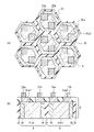
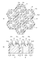
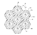
- 4 is a plan view showing an example of pixel arrangement in a pixel array section according to the first embodiment
- FIG. It is a figure which shows an example at the time of comparing the 1st Embodiment and a comparative example.
- FIG. 4 is a diagram showing a process flow (part 1) for forming a pixel according to the first embodiment
- FIG. 10 is a diagram showing a process flow (part 2) for forming pixels according to the first embodiment
- FIG. 3 is a diagram showing a process flow (part 3) for forming pixels according to the first embodiment
- FIG. 4 is a diagram showing a process flow (part 4) for forming pixels according to the first embodiment
- FIG. 10 is a plan view showing an example of arranging an on-chip lens for each pixel in a comparative example of a modified example of the first embodiment
- FIG. 11 is a plan view showing an example of arranging an on-chip lens for each pixel in a modification of the first embodiment
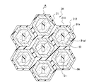
- FIG. 10 is a plan view showing an example of pixels arranged in a pixel array section in a solid-state imaging device according to a second embodiment of the present technology
- 2 is a cross-sectional view of a pixel taken along the dashed-dotted line A-A' in FIG. 1 in the vertical direction in the second embodiment
- FIG. FIG. 11 is a plan view showing an example of pixels arranged in a pixel array section in a modification of the second embodiment
- FIG. 11 is a plan view showing an example of pixels arranged in a pixel array section in a solid-state imaging device according to a third embodiment of the present technology
- 2 is a cross-sectional view of a pixel taken along the dashed-dotted line A-A' in FIG.
- FIG. 11 is a plan view showing an example of pixels arranged in a pixel array section in a first modification of the third embodiment
- FIG. 11 is a plan view showing an example of pixels arranged in a pixel array section in a second modification of the third embodiment
- FIG. 11 is a plan view showing an example of pixels arranged in a pixel array section in a third modification of the third embodiment
- 1 is a block diagram showing a configuration example of an embodiment of an imaging device as an electronic device to which the present technology is applied;
- first conductivity type is one of p-type or n-type
- second conductivity type means one of p-type or n-type, which is different from “first conductivity type”.
- first conductivity type is one of p-type or n-type
- second conductivity type means one of p-type or n-type, which is different from “first conductivity type”.
- +" and “-” attached to "n” and “p” refer to semiconductor regions having relatively high or low impurity densities, respectively, compared to semiconductor regions not marked with “+” and “-”. It means to be an area. However, even if the same "n” is attached to the semiconductor region, it does not mean that the impurity density of each semiconductor region is exactly the same.
- each pixel is configured to have a regular hexagonal outer edge shape in plan view (or in a plane parallel to the aperture surface (principal surface) of the pixel).
- the outer edge shape of the pixel is a regular hexagon will be described.
- the term “outer edge shape” refers to the geometric shape of the outer edge of an object in plan view, and the term “plan view” is omitted when the meaning is clear in the context. may be
- FIG. 1 is a schematic configuration diagram showing the entire solid-state imaging device 1 according to the first embodiment of the present technology.
- the solid-state imaging device 1 in FIG. 1 is a back-illuminated CMOS (Complementary Metal Oxide Semiconductor) image sensor.
- CMOS Complementary Metal Oxide Semiconductor
- the solid-state imaging device 1 takes in image light from a subject through an optical lens, converts the amount of incident light formed on an imaging surface into an electric signal on a pixel-by-pixel basis, and outputs the electric signal as a pixel signal.
- the solid-state imaging device 1 of the first embodiment includes a substrate 2, a pixel array section 3, a vertical drive circuit 4, a column signal processing circuit 5, a horizontal drive circuit 6, and an output circuit. 7 and a control circuit 8 .
- the pixel array section 3 has a plurality of pixels 9 regularly arranged in a two-dimensional array on the substrate 2 .
- Each pixel 9 in the pixel array section 3 has a regular hexagonal shape in plan view, and is arranged in an array to form a honeycomb structure.
- the vertical drive circuit 4 is composed of, for example, a shift register, selects a desired pixel drive wiring 10, supplies a pulse for driving the pixels 9 to the selected pixel drive wiring 10, and drives each pixel 9 in units of rows. drive. That is, the vertical driving circuit 4 sequentially selectively scans the pixels 9 of the pixel array section 3 in the vertical direction row by row, and generates pixel signals based on signal charges generated by the photoelectric conversion sections of the pixels 9 according to the amount of received light. , to the column signal processing circuit 5 through the vertical signal line 11 .
- the column signal processing circuit 5 is arranged, for example, for each column of the pixels 9, and performs signal processing such as noise removal on the signals output from the pixels 9 of one row for each pixel column.
- the column signal processing circuit 5 performs signal processing such as CDS (Correlated Double Sampling) and AD (Analog Digital) conversion for removing pixel-specific fixed pattern noise.
- the horizontal driving circuit 6 is composed of, for example, a shift register, sequentially outputs horizontal scanning pulses to the column signal processing circuits 5, selects each of the column signal processing circuits 5 in order, and from each of the column signal processing circuits 5, The pixel signal subjected to the signal processing is output to the horizontal signal line 12 .
- the output circuit 7 performs signal processing on pixel signals sequentially supplied from each of the column signal processing circuits 5 through the horizontal signal line 12 and outputs the processed pixel signals.
- signal processing for example, buffering, black level adjustment, column variation correction, and various digital signal processing can be used.
- the control circuit 8 generates a clock signal and a control signal that serve as references for the operation of the vertical drive circuit 4, the column signal processing circuit 5, the horizontal drive circuit 6, etc. based on the vertical synchronization signal, the horizontal synchronization signal, and the master clock signal. Generate. The control circuit 8 then outputs the generated clock signal and control signal to the vertical drive circuit 4, the column signal processing circuit 5, the horizontal drive circuit 6, and the like.
- FIG. 2 shows an equivalent circuit of the pixel 9.
- the pixel 9 includes a photodiode (PD) 91a, a transfer transistor (TG) 91b, a floating diffusion (FD) portion 91c, a conversion efficiency adjustment transistor (FDG) 91d, an amplification transistor (AMP) 91e, a selection transistor ( SEL) 91f and a reset transistor (RST) 91g.
- the transfer transistor 91b, the conversion efficiency adjustment transistor 91d, the amplification transistor 91e, the selection transistor 91f, and the reset transistor 91g are composed of MOS transistors, for example.
- the photodiode 91a constitutes a photoelectric conversion section that photoelectrically converts incident light.
- the anode of the photodiode 91a is grounded.
- the source of the transfer transistor 91b is connected to the cathode of the photodiode 91a.
- the drain of the transfer transistor 91b is connected to the FD section 91c.
- the transfer transistor 91b transfers the signal charge from the photodiode 91a to the FD portion 91c based on the transfer signal applied to the gate.
- the FD portion 91c accumulates signal charges transferred from the photodiode 91a via the transfer transistor 91b.
- the potential of the FD portion 91c is modulated according to the signal charge amount accumulated in the FD portion 91c.
- the source of the conversion efficiency adjustment transistor 91d is connected to the FD section 91c.
- the drain of the conversion efficiency adjustment transistor 91d is connected to the source of the reset transistor 91g.
- the conversion efficiency adjustment transistor 91d adjusts the conversion efficiency of the signal charges according to the conversion efficiency adjustment signal applied to the gate.
- the gate of the amplification transistor 91e is connected to the FD section 91c.
- the source of the selection transistor 91f is connected to the drain of the amplification transistor 91e.
- a power supply potential (VDD) is applied to the source of the amplification transistor 91e.
- the amplification transistor 91e amplifies the potential of the FD section 91c.
- a power supply potential (VDD) is applied to the drain of the reset transistor 91g.
- the reset transistor 91g initializes (resets) signal charges accumulated in the FD section 91c based on a reset signal applied to the gate.
- a drain of the selection transistor 91f is connected to the vertical signal line 11 .
- the selection transistor 91f selects the pixel 9 based on the selection signal applied to the gate. When the pixel 9 is selected, a pixel signal corresponding to the potential amplified by the amplification transistor 91 e is output through the vertical signal line 11 .
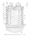
- FIG. 3 shows a cross-sectional view of the pixel 9 taken along the dashed-dotted line AA' passing through the pixel 9 in FIG. 1 in the vertical direction.
- the surface on the light incident surface side (lower side in FIG. 3) of each member of the solid-state imaging device 1 will be referred to as the “back surface”, and the side opposite to the light incident surface side of each member of the solid-state imaging device 1 (on the side in FIG. 3). upper side) is called the "surface”.
- a photodiode 91 a is formed on the substrate 2 of the solid-state imaging device 1 .
- the substrate 2 for example, a semiconductor substrate made of silicon (Si) can be used.
- the photodiode 91 a has an n-type semiconductor region 91 a 1 and a p-type semiconductor region 91 a 2 formed on the surface side of the substrate 2 .
- signal charges corresponding to the amount of incident light are generated, and the generated signal charges are accumulated in the n-type semiconductor region 91a1.
- each pixel 9 is electrically isolated by the inter-pixel isolation section 31 .
- the inter-pixel separation part 31 is formed in the depth direction from the back surface side of the substrate 2, as shown in FIG.
- the inter-pixel separation portion 31 is formed in a lattice shape so as to surround each pixel 9, as will be described later.
- an insulating film is embedded in the inter-pixel separation section 31 to improve the light shielding performance.
- a pinning region 19 to be a p-type semiconductor region implanted with boron is formed between the side wall of the inter-pixel isolation portion 31 and the n-type semiconductor region 91a1. Electrons that cause dark current are absorbed by holes that are majority carriers in the pinning region 19, thereby suppressing the dark current.
- the on-chip lens 18 converges the irradiation light and makes the condensed light efficiently enter the photodiode 91 a in the substrate 2 via the color filter 17 .
- the on-chip lens 18 can be constructed of an insulating material that does not have light absorption properties. Silicon oxide, silicon nitride, silicon oxynitride, organic SOG, polyimide-based resin, fluorine-based resin, and the like are examples of insulating materials that do not have light absorption properties.
- the color filter 17 transmits the wavelength of light to be received by each pixel 9 and causes the transmitted light to enter the photodiode 91 a in the substrate 2 .
- the wiring layer 40 is formed on the surface side of the substrate 2, and includes a transfer transistor 91b as a pixel transistor, a floating diffusion portion 91c, a conversion efficiency adjustment transistor 91d, an amplification transistor 91e, a selection transistor 91f, a reset transistor 91g, and wiring. consists of In the example of FIG. 3, the transfer transistor 91b, the floating diffusion portion 91c, and the amplification transistor 91e are illustrated as representatives.
- the solid-state imaging device 1 having the above configuration, light is irradiated from the back side of the substrate 2, the irradiated light is transmitted through the on-chip lens 18 and the color filter 17, and the transmitted light is photoelectrically converted by the photodiode 91a. Thus, signal charges are generated. Then, the generated signal charge is output as a pixel signal through the pixel transistor formed in the wiring layer 40 to the vertical signal line 11 shown in FIG.
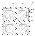
- FIG. 4 is a plan view showing an example of the pixel array section B3 in the comparative example.
- a plurality of pixels B9 are arranged at equal pitches in the row and column directions.
- the plurality of pixels B9 are electrically isolated by an inter-pixel isolation portion B31.
- the inter-pixel separation portion B31 is formed in a lattice shape so as to surround each pixel B9.
- an n-type semiconductor region B91a1 of a photodiode B91a is formed at the center position.
- a pinning region B19 to be a p-type semiconductor region is formed between the pixel separation portion B31 and the n-type semiconductor region B91a1.
- the corner portion B312 where the side B311 of the inter-pixel separation portion B31 intersects is a right angle. , the penetration of boron and the application of the electric field become rounded. Therefore, the n-type semiconductor region B91a1 of the photodiode B91a becomes smaller.
- the outer edge shape of the pixel 9 is a regular hexagon so that the corner portion 312 where the side 311 of the inter-pixel separation portion 31 intersects has an obtuse angle (90 degrees or more). It has a rectangular shape.
- the inter-pixel separation part 31 is formed in a lattice shape so as to surround each regular hexagonal pixel 9 .
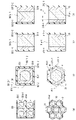
- FIG. 6 is a diagram showing an example of comparison between the first embodiment and a comparative example.
- FIG. 6A shows a state in which a plurality of pixels B9 are arranged in the comparative example and a state in which a plurality of pixels 9 are arranged in the first embodiment.
- one pixel B9 has a square outer edge shape, and is composed of four sides B311 and four corners B312 where the four sides B311 intersect.
- one pixel 9 has a regular hexagonal outer edge and consists of six sides 311 and six corners 312 where the six sides 311 intersect.
- FIG. 6C shows a cross section between sides B311-1 and B311-2 of pixel B9 in the comparative example, and a cross section between sides 311-1 and 311-2 of pixel 9 in the first embodiment. shows a cross-section between In FIG. 6C, the n-type semiconductor region B91a1 of the comparative example and the n-type semiconductor region 91a1 of the first embodiment are substantially equal.
- FIG. 6D shows a cross section between the corner portions B312-1 and B312-2 of the pixel B9 in the comparative example, and the corner portions 312-1 and 312 of the pixel 9 in the first embodiment. -2.
- the n-type semiconductor region B91a1 of the comparative example and the n-type semiconductor region 91a1 of the first embodiment are wider than the n-type semiconductor region B91a1 of the comparative example. Therefore, by forming the outer edge shape of the pixel 9 into a regular hexagonal shape, it is possible to reduce the overlap of the p-type semiconductor regions at the corner portions 312 and reduce the decrease in the n-type semiconductor regions 91a1.
- FIG. 7A the inter-pixel isolation part 31 is formed along the outer edge shape of the pixel 9 .
- FIG. 7B grooves are formed in the depth direction from the rear surface side of the substrate 2 between the adjacent pixels 9, and an insulating film is embedded in the grooves to form the inter-pixel isolation part 31.
- a pinning region 19 is formed by implanting boron into the side wall of the inter-pixel isolation portion 31 .
- the pinning region 19 is formed in the depth direction from the back side of the substrate 2, as shown in FIG. 8(b).
- gate electrodes 21a and 21b are formed in each pixel 9.
- the gate electrodes 21a and 21b are formed on the surface of the substrate 2, as shown in FIG. 9(b).
- a contact 22 made of wiring is formed in each pixel 9.
- the conversion efficiency adjustment transistor 91d, amplification transistor 91e, selection transistor 91f, and reset transistor 91g are shared by four pixels 9 arranged in two rows and two columns.
- Contacts 22 are also formed on the upper surfaces of the gate electrodes 21a and 21b.
- the contacts 22 are formed on the surface of the substrate 2, as shown in FIG. 10(b). These gate electrodes 21a and 21b and contact 22 form a transfer transistor 91b, an amplification transistor 91e, and a reset transistor 91g. A contact 22 between the transfer transistor 91b and the amplification transistor 91e forms an FD portion 91c. Further, the FD portion 91c is formed by the contact 22 between the transfer transistor 91b and the reset transistor 91g.
- the pixel array section 3 can have a honeycomb structure, thereby increasing the density of the pixels 9 per unit area. is increased, and efficient light collection becomes possible. Further, by forming the outer edge of the pixel 9 into a regular hexagonal shape, the angle of the corner portion 312 formed by the adjacent sides 311 becomes an obtuse angle, thereby suppressing the reduction of the n-type semiconductor region 91a1 of the photodiode 91a. Since the reduction of the n-type semiconductor region 91a1 can be suppressed, an improvement in the amount of signal charge (Qs) can be expected particularly in the fine pixels 9.
- Qs signal charge
- a modification of the first embodiment describes the arrangement of the on-chip lens 18 .
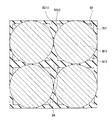
- FIG. 11 is a plan view showing an example of arranging an on-chip lens B18 for each pixel B9 in a comparative example. 11, the same parts as in FIG. 4 are denoted by the same reference numerals, and detailed description thereof will be omitted. As shown in FIG. 11, a plurality of pixels B9 are arranged at equal pitches in the row and column directions. When the on-chip lens B18 is arranged for each pixel 9, an optically ineffective invalid area BA is formed between adjacent on-chip lenses B18.
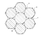
- the outer edge shape of the pixels 9 is a regular hexagon, and the pixels 9 are arranged to form a honeycomb structure, thereby forming an ineffective area of the on-chip lens 18 as shown in FIG. BA can be reduced.
- a pixel 9A has a dual pixel structure in which an n-type semiconductor region 91a1 and a p-type semiconductor region 91a2 of a photodiode 91a are separated into two by an intra-pixel separating portion.
- FIG. 13 is a plan view showing an example of pixels 9A arranged in the pixel array section 3A in the solid-state imaging device 1A according to the second embodiment. 13, the same parts as in FIG. 5 are denoted by the same reference numerals, and detailed description thereof will be omitted.
- a trench (FFTI) 51 is formed as an intra-pixel isolation section in the pixel 9A.
- the trench 51 contains a metal film or an oxide film.
- the trench 51 is positioned at the center of the pixel 9A and formed from the center of the pixel 9A toward the side 311 of the inter-pixel isolation portion 31. As shown in FIG.
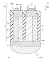
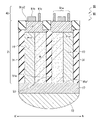
- FIG. 14 shows a cross-sectional view of the pixel 9A cut along the dashed-dotted line AA' in FIG. 1 in the vertical direction.
- the trench 51 is formed from the front surface to the rear surface of the substrate 2 of the pixel 9A.
- FIG. 15 is a plan view showing an example of pixels 9A arranged in the pixel array section 3A in the modification of the second embodiment. 15, the same parts as in FIG. 13 are denoted by the same reference numerals, and detailed description thereof will be omitted.
- a trench (FFTI) 52 is formed in the pixel 9A.
- the trench 52 contains a metal film or an oxide film.
- the trench 52 is positioned at the center of the pixel 9A and formed from the center of the pixel 9A toward the corner portion 312 of the inter-pixel isolation portion 31. As shown in FIG.
- a pixel 9B has a dual pixel structure in which an n-type semiconductor region 91a1 and a p-type semiconductor region 91a2 of a photodiode 91a are separated into two by an intra-pixel separating portion.
- FIG. 16 is a plan view showing an example of pixels 9B arranged in the pixel array section 3B in the solid-state imaging device 1B according to the third embodiment. 16, the same parts as in FIG. 13 are denoted by the same reference numerals, and detailed description thereof will be omitted.
- a trench (RDTI) 53 is formed as an intra-pixel isolation section in the pixel 9B.
- the trench 53 contains a metal film or an oxide film.
- the trench 53 is positioned at the center of the pixel 9B and formed from the center of the pixel 9B toward the side 311 of the inter-pixel isolation portion 31 .
- FIG. 17 shows a cross-sectional view of the pixel 9B cut along the dashed-dotted line AA' in FIG. 1 in the vertical direction.
- the trench 53 is formed from the back surface to the front surface of the substrate 2 of the pixel 9B.
- the same effects as those of the first embodiment can be obtained, and the n-type semiconductor region 91a1 of the photodiode 91a can be reduced even if the same-color isolation is performed by the trench 53. can be suppressed.
- FIG. 18 is a plan view showing an example of pixels 9B arranged in the pixel array section 3B in the first modification of the third embodiment. 18, the same parts as in FIG. 16 are denoted by the same reference numerals, and detailed description thereof will be omitted.
- a trench (RDTI) 54 is formed in the pixel 9B.
- the trench 54 contains a metal film or an oxide film.
- the trench 54 is positioned at the center of the pixel 9B and formed from the center of the pixel 9B toward the corner portion 312 of the inter-pixel isolation portion 31 .
- FIG. 19 is a plan view showing an example of pixels 9B arranged in the pixel array section 3B in the second modification of the third embodiment. 19, the same parts as in FIG. 16 are denoted by the same reference numerals, and detailed description thereof will be omitted.
- Trench (RDTI) 551 and 552 are formed in the pixel 9B.
- the trenches 551 and 552 contain metal films or oxide films.
- the trench 551 is positioned on the side 311-1 of the inter-pixel isolation portion 31 of the pixel 9B and formed from the side 311-1 toward the center of the pixel 9B.
- the trench 552 is located on the side 311-2 of the inter-pixel isolation portion 31 of the pixel 9B and formed from the side 311-2 toward the center of the pixel 9B.
- FIG. 20 is a plan view showing an example of pixels 9B arranged in the pixel array section 3B in the third modification of the third embodiment. 20, the same parts as in FIG. 16 are denoted by the same reference numerals, and detailed description thereof will be omitted.
- Trench (RDTI) 561 and 562 are formed in the pixel 9B.
- the trenches 561 and 562 contain metal films or oxide films.
- the trench 561 is positioned at the corner portion 312-1 of the inter-pixel isolation portion 31 of the pixel 9B and formed from the corner portion 312-1 toward the center of the pixel 9B.
- the trench 562 is positioned at the corner portion 312-2 of the inter-pixel isolation portion 31 of the pixel 9B and formed from the corner portion 312-2 toward the center of the pixel 9B.
- the present technology can be achieved by the first to third embodiments, the modified example of the first embodiment, the modified example of the second embodiment, and the first to third modified examples of the third embodiment.
- the discussion and drawings forming part of this disclosure should not be understood as limiting the technology.
- the gist of the technical contents disclosed by the first to third embodiments, the modified example of the first embodiment, the modified example of the second embodiment, and the first to third modified examples of the third embodiment it will be apparent to those skilled in the art that various alternative embodiments, implementations and operating techniques may be included in the present technology.
- the configurations disclosed in the first to third embodiments, the modified example of the first embodiment, the modified example of the second embodiment, and the first to third modified examples of the third embodiment are They can be appropriately combined within a range that does not cause contradiction.
- configurations disclosed by a plurality of different embodiments may be combined, or configurations disclosed by a plurality of different modifications of the same embodiment may be combined.
- FIG. 21 is a block diagram showing a configuration example of an embodiment of an imaging device as an electronic device to which the present technology is applied.
- An imaging device 1000 in FIG. 21 is a video camera, a digital still camera, or the like.
- the imaging apparatus 1000 comprises a lens group 1001 , a solid-state imaging device 1002 , a DSP circuit 1003 , a frame memory 1004 , a display section 1005 , a recording section 1006 , an operation section 1007 and a power supply section 1008 .
- DSP circuit 1003 , frame memory 1004 , display unit 1005 , recording unit 1006 , operation unit 1007 and power supply unit 1008 are interconnected via bus line 1009 .
- a lens group 1001 captures incident light (image light) from a subject and forms an image on the imaging surface of the solid-state imaging device 1002 .
- the solid-state image pickup device 1002 consists of the first to fourteenth embodiments of the solid-state image pickup device described above.
- the solid-state imaging device 1002 converts the amount of incident light, which is imaged on the imaging surface by the lens group 1001, into an electric signal for each pixel and supplies the electric signal to the DSP circuit 1003 as a pixel signal.
- the DSP circuit 1003 performs predetermined image processing on the pixel signals supplied from the solid-state imaging device 1002, and supplies the image signals after the image processing to the frame memory 1004 in units of frames for temporary storage.
- the display unit 1005 is composed of a panel-type display device such as a liquid crystal panel or an organic EL (Electro Luminescence) panel, and displays an image based on the frame-by-frame pixel signals temporarily stored in the frame memory 1004 .
- a recording unit 1006 is composed of a DVD (Digital Versatile Disk), a flash memory, or the like, and reads and records pixel signals in frame units temporarily stored in the frame memory 1004 .
- An operation unit 1007 issues operation commands for various functions of the imaging apparatus 1000 under user's operation.
- the power supply unit 1008 appropriately supplies power to the DSP circuit 1003 , the frame memory 1004 , the display unit 1005 , the recording unit 1006 and the operation unit 1007 .
- the electronic device to which the present technology is applied may be any device that uses a photodetector in its image capture unit (photoelectric conversion unit). There are copiers and the like that use devices.
- a pixel array section in which a plurality of pixels capable of generating an electric signal in response to light incident from the outside are arranged in an array, each of the plurality of pixels, a first conductivity type photoelectric conversion region that photoelectrically converts the incident light; an inter-pixel separation section that defines an outer edge shape of the pixel and insulates and separates the adjacent pixels; a pinning region of a second conductivity type opposite to the first conductivity type formed between the photoelectric conversion region and a sidewall of the inter-pixel isolation portion;
- the plurality of pixels are arranged in an array so as to form a honeycomb structure in which the corners where the plurality of sides intersect are obtuse angles in a plan view, Light receiving element.
- the outer edge shape of the pixel is a regular hexagon, The light receiving element according to (1) above.
- the intra-pixel isolation section is a first trench containing a metal film or an oxide film formed from a surface opposite to the incident side of the pixel toward the incident side.
- the first trench is positioned at the center of the pixel and is formed from the center of the pixel toward at least one corner of the inter-pixel isolation section.
- the intra-pixel isolation section is a second trench containing a metal film or an oxide film formed from a surface of the pixel on the incident side to a surface opposite to the incident side. element.
- the second trench is positioned at the center of the pixel and is formed from the center of the pixel toward at least one corner of the inter-pixel isolation section.
- the plurality of pixels includes light receiving elements arranged in an array so as to form a honeycomb structure in which corners where a plurality of sides intersect are obtuse angles in plan view, Electronics.
- conversion efficiency adjustment transistor 91e... amplification transistor, 91f... selection transistor, 91g... reset transistor, 311, 311- 1,311-2...side 312,312-1,312-2...corner part 1000...imaging device 1001...lens group 1002...solid-state image sensor 1003...DSP circuit 1004...frame memory 1005...display Section 1006 Recording section 1007 Operation section 1008 Power supply section 1009 Bus line.
Landscapes
- Solid State Image Pick-Up Elements (AREA)
- Light Receiving Elements (AREA)
- Transforming Light Signals Into Electric Signals (AREA)
Abstract
Description
なお、本明細書中に記載される効果はあくまで例示であって限定されるものでは無く、また他の効果があってもよい。
本開示では、各画素が、平面視で(又は画素の開口面(主面)に平行な面において)、正六角形形状の外縁形状を有するように構成された、アレイ型の受光素子が説明される。とりわけ、本実施形態では、画素の外縁形状が正六角形形状である例が説明される。なお、本開示において、「外縁形状」とは、平面視での物体の外縁の幾何学的形状をいい、文脈上、その意味であることが明らかなときは、「平面視」といった語が省略されることがある。
本技術の第1の実施形態に係る受光素子としての固体撮像装置1について説明する。図1は、本技術の第1の実施形態に係る固体撮像装置1の全体を示す概略構成図である。
画素アレイ部3は、基板2上に、2次元アレイ状に規則的に配列された複数の画素9を有している。画素アレイ部3における各画素9は、平面視で、正六角形形状を有し、ハニカム構造をなすようにアレイ状に配置される。
出力回路7は、カラム信号処理回路5の各々から水平信号線12を通して、順次に供給される画素信号に対し信号処理を行って出力する。信号処理としては、例えば、バファリング、黒レベル調整、列ばらつき補正、各種デジタル信号処理等を用いることができる。
図2は、画素9の等価回路を示す。
画素9は、フォトダイオード(PD)91a、転送トランジスタ(TG)91b、浮遊拡散(フローティング・ディフュージョン(FD))部91c、変換効率調整トランジスタ(FDG)91d、増幅トランジスタ(AMP)91e、選択トランジスタ(SEL)91f、リセットトランジスタ(RST)91gを含む。転送トランジスタ91b、変換効率調整トランジスタ91d、増幅トランジスタ91e、選択トランジスタ91f、リセットトランジスタ91gは、例えばMOSトランジスタで構成されている。
転送トランジスタ91bのドレインは、FD部91cに接続される。転送トランジスタ91bは、ゲートに印加される転送信号に基づき、フォトダイオード91aからの信号電荷をFD部91cに転送する。
FD部91cには、変換効率調整トランジスタ91dのソースが接続されている。変換効率調整トランジスタ91dのドレインは、リセットトランジスタ91gのソースに接続されている。変換効率調整トランジスタ91dは、ゲートに印加される変換効率調整信号に応じて、信号電荷の変換効率を調整する。
選択トランジスタ91fのドレインは、垂直信号線11に接続されている。選択トランジスタ91fは、ゲートに印加される選択信号に基づき、画素9を選択する。画素9が選択された場合、増幅トランジスタ91eにより増幅された電位に応じた画素信号が垂直信号線11を介して出力される。
図3は、図1の画素9を通る一点鎖線A-A’を垂直方向に切断した画素9の断面図を示している。
以下、固体撮像装置1の各部材の光入射面側(図3の下側)の面を「裏面」と呼び、固体撮像装置1の各部材の光入射面側とは反対側(図3の上側)の面を「表面」と呼ぶ。
固体撮像装置1の基板2には、フォトダイオード91aが形成されている。基板2としては、例えば、シリコン(Si)からなる半導体基板を使用できる。フォトダイオード91aは、n型半導体領域91a1と、基板2の表面側に形成されたp型半導体領域91a2とを有している。フォトダイオード91aでは、入射された光の光量に応じた信号電荷が生成され、生成された信号電荷がn型半導体領域91a1に蓄積される。
カラーフィルタ17は、各画素9に受光させたい光の波長を透過させ、透過させた光を基板2内のフォトダイオード91aに入射させる。
図4は、比較例における画素アレイ部B3の一例を示す平面図である。図4に示すように、複数の画素B9が行方向及び列方向に等ピッチで配列されている。複数の画素B9の間は、画素間分離部B31により電気的に分離されている。画素間分離部B31は、各画素B9を取り囲むように格子状に形成されている。
比較例では、画素B9が正方形であるために、画素間分離部B31の辺B311が交わるコーナー部B312が直角であり、画素間分離部B31からピニング領域B19を形成する際には、コーナー部B312でホウ素(Boron)の侵入や電界のかかり方が丸くなる。このため、フォトダイオードB91aのn型半導体領域B91a1が小さくなる。
本技術の第1の実施形態では、図5に示すように、画素9の外縁形状を、画素間分離部31の辺311が交わるコーナー部312が鈍角(90度以上)になるように、正六角形形状としている。画素間分離部31は、正六角形形状の各画素9を取り囲むように格子状に形成されている。
1つの画素B9は、図6(b)に示すように、その外縁形状が正方形で、4つの辺B311と、4つの辺B311それぞれが交わる4つのコーナー部B312とから成る。一方、1つの画素9は、図6(b)に示すように、その外縁形状が正六角形で、6つの辺311と、6つの辺311それぞれが交わる6つのコーナー部312とから成る。
従って、画素9の外縁形状を正六角形形状にすることで、コーナー部312でのp型半導体領域の重なりを小さくでき、n型半導体領域91a1の減少を低減できる。
図7乃至図10は、第1の実施形態に係る画素9を形成するためのプロセスフローを示す。
図7(a)に示すように、画素9の外縁形状に沿って、画素間分離部31を形成する。この場合、図7(b)に示すように、隣接する画素9の間に、基板2の裏面側から深さ方向に溝部を形成し、溝部に絶縁膜を埋め込むことにより、画素間分離部31を形成する。
次に、図9(a)に示すように、各画素9にゲート電極21a,21bを形成する。ゲート電極21a,21bは、図9(b)に示すように、基板2の表面に形成される。
以上のように第1の実施形態によれば、画素9の外縁形状が正六角形形状であるため、画素アレイ部3はハニカム構造を有することができ、これにより、単位面積当たりの画素9の密度を高め、効率的な集光ができるようになる。また、画素9の外縁形状を正六角形形状にすることで、隣接する辺311がなすコーナー部312の角度が鈍角となり、これによりフォトダイオード91aのn型半導体領域91a1の減少を抑えることができる。n型半導体領域91a1の減少を抑えることができるため、特に微細の画素9において信号電荷量(Qs)の向上が期待できる。
第1の実施形態の変形例は、上記オンチップレンズ18の配置について説明する。
図11は、比較例における画素B9ごとにオンチップレンズB18を配置する一例を示す平面図である。なお、図11において、上記図4と同一部分については同一符号を付して詳細な説明を省略する。
図11に示すように、複数の画素B9が行方向及び列方向に等ピッチで配列されている。画素9ごとにオンチップレンズB18を配置すると、隣接するオンチップレンズB18の間は、光学的に無効となる無効領域BAになる。
第1の実施形態の変形例では、画素9の外縁形状が正六角形形状であり、各画素9が配列してハニカム構造をなすことにより、図12に示すように、オンチップレンズ18の無効領域BAを減らすことが可能となる。
第2の実施形態は、画素9Aにおいて、フォトダイオード91aのn型半導体領域91a1及びp型半導体領域91a2を画素内分離部により2つに分離するデュアルピクセル構造を有する場合について説明する。
画素9Aには、画素内分離部としてトレンチ(FFTI)51が形成されている。トレンチ51は、金属膜または酸化膜を含むものである。トレンチ51は、画素9Aの中心に位置し、画素9Aの中心から画素間分離部31の辺311に向かって形成される。
トレンチ51は、画素9Aの基板2の表面から裏面側へ形成される。
以上のように第2の実施形態によれば、上記第1の実施形態と同様の作用効果が得られ、トレンチ51により同色間分離を行っても、フォトダイオード91aのn型半導体領域91a1の減少を抑えることができる。
図15は、第2の実施形態の変形例において、画素アレイ部3Aに配列した画素9Aの一例を示す平面図である。なお、図15において、上記図13と同一部分には同一符号を付して詳細な説明を省略する。
第3の実施形態は、画素9Bにおいて、フォトダイオード91aのn型半導体領域91a1及びp型半導体領域91a2を画素内分離部により2つに分離するデュアルピクセル構造を有する場合について説明する。
画素9Bには、画素内分離部としてトレンチ(RDTI)53が形成されている。トレンチ53は、金属膜または酸化膜を含むものである。トレンチ53は、画素9Bの中心に位置し、画素9Bの中心から画素間分離部31の辺311に向かって形成される。
トレンチ53は、画素9Bの基板2の裏面から表面側へ形成される。
以上のように第3の実施形態によれば、上記第1の実施形態と同様の作用効果が得られ、トレンチ53により同色間分離を行っても、フォトダイオード91aのn型半導体領域91a1の減少を抑えることができる。
図18は、第3の実施形態の第1の変形例において、画素アレイ部3Bに配列した画素9Bの一例を示す平面図である。なお、図18において、上記図16と同一部分には同一符号を付して詳細な説明を省略する。
図19は、第3の実施形態の第2の変形例において、画素アレイ部3Bに配列した画素9Bの一例を示す平面図である。なお、図19において、上記図16と同一部分には同一符号を付して詳細な説明を省略する。
図20は、第3の実施形態の第3の変形例において、画素アレイ部3Bに配列した画素9Bの一例を示す平面図である。なお、図20において、上記図16と同一部分には同一符号を付して詳細な説明を省略する。
上記のように、本技術は第1から第3の実施形態、第1の実施形態の変形例、第2の実施形態の変形例、第3の実施形態の第1乃至第3の変形例によって記載したが、この開示の一部をなす論述及び図面は本技術を限定するものであると理解すべきではない。上記の第1から第3の実施形態、第1の実施形態の変形例、第2の実施形態の変形例、第3の実施形態の第1乃至第3の変形例が開示する技術内容の趣旨を理解すれば、当業者には様々な代替実施形態、実施例及び運用技術が本技術に含まれ得ることが明らかとなろう。また、第1から第3の実施形態、第1の実施形態の変形例、第2の実施形態の変形例、第3の実施形態の第1乃至第3の変形例がそれぞれ開示する構成を、矛盾の生じない範囲で適宜組み合わせることができる。例えば、複数の異なる実施形態がそれぞれ開示する構成を組み合わせてもよく、同一の実施形態の複数の異なる変形例がそれぞれ開示する構成を組み合わせてもよい。
図21は、本技術を適用した電子機器としての撮像装置の一実施形態の構成例を示すブロック図である。
図21の撮像装置1000は、ビデオカメラやデジタルスチルカメラ等である。撮像装置1000は、レンズ群1001、固体撮像素子1002、DSP回路1003、フレームメモリ1004、表示部1005、記録部1006、操作部1007、および電源部1008からなる。DSP回路1003、フレームメモリ1004、表示部1005、記録部1006、操作部1007、および電源部1008は、バスライン1009を介して相互に接続されている。
表示部1005は、例えば、液晶パネルや有機EL(Electro Luminescence)パネル等のパネル型表示装置からなり、フレームメモリ1004に一時的に記憶されたフレーム単位の画素信号に基づいて、画像を表示する。
操作部1007は、ユーザによる操作の下に、撮像装置1000が持つ様々な機能について操作指令を発する。電源部1008は、電源を、DSP回路1003、フレームメモリ1004、表示部1005、記録部1006、および操作部1007に対して適宜供給する。
(1)
外部から入射した光に応じて電気信号を生成可能な複数の画素がアレイ状に配置された画素アレイ部を備え、
前記複数の画素のそれぞれは、
入射した前記光を光電変換する第1導電型の光電変換領域と、
前記画素の外縁形状を規定し、隣接する前記画素間を絶縁して分離する画素間分離部と、
前記光電変換領域と前記画素間分離部の側壁との間に形成される、前記第1導電型とは逆の第2導電型のピニング領域と
を備え、
前記複数の画素は、平面視において、複数の辺が交わる角部が鈍角となるハニカム構造をなすようにアレイ状に配置される、
受光素子。
(2)
前記画素の外縁形状は、正六角形形状である、
上記(1)に記載の受光素子。
(3)
前記複数の画素のそれぞれは、前記光電変換領域を画素内分離部により2つに分離するデュアルピクセル構造である
上記(1)に記載の受光素子。
(4)
前記画素内分離部は、前記画素の入射側とは反対側の面から前記入射側へ形成される、金属膜または酸化膜を含む第1のトレンチである
上記(3)に記載の受光素子。
(5)
前記第1のトレンチは、前記画素の中心に位置し、前記画素の中心から前記画素間分離部の少なくとも1つの角部に向かって形成される
上記(4)に記載の受光素子。
(6)
前記第1のトレンチは、前記画素の中心に位置し、前記画素の中心から前記画素間分離部の少なくともの1つの辺に向かって形成される
上記(4)に記載の受光素子。
(7)
前記画素内分離部は、前記画素の入射側の面から前記入射側とは反対側の面へ形成される、金属膜または酸化膜を含む第2のトレンチである
上記(3)に記載の受光素子。
(8)
前記第2のトレンチは、前記画素の中心に位置し、前記画素の中心から前記画素間分離部の少なくとも1つの角部に向かって形成される
上記(7)に記載の受光素子。
(9)
前記第2のトレンチは、前記画素の中心に位置し、前記画素の中心から前記画素間分離部の少なくとも1つの辺に向かって形成される
上記(7)に記載の受光素子。
(10)
前記第2のトレンチは、前記画素間分離部の少なくとも1つの角部に位置し、前記画素間分離部の角部から前記画素の中心に向かって形成される
上記(7)に記載の受光素子。
(11)
前記第2のトレンチは、前記画素間分離部の少なくとも1つの辺に位置し、前記画素間分離部の辺から前記画素の中心に向かって形成される
上記(7)に記載の受光素子。
(12)
前記画素アレイ部は、前記画素ごとに形成され、前記光が前記画素に集光するように形成されたオンチップレンズをさらに備える
上記(1)に記載の受光素子。
(13)
外部から入射した光に応じて電気信号を生成可能な複数の画素がアレイ状に配置された画素アレイ部を備え、
前記複数の画素のそれぞれは、
入射した前記光を光電変換する第1導電型の光電変換領域と、
前記画素の外縁形状を規定し、隣接する前記画素間を絶縁して分離する画素間分離部と、
前記光電変換領域と前記画素間分離部の側壁との間に形成される、前記第1導電型とは逆の第2導電型のピニング領域と
を備え、
前記複数の画素は、平面視において、複数の辺が交わる角部が鈍角となるハニカム構造をなすようにアレイ状に配置される、受光素子を備えた、
電子機器。
Claims (13)
- 外部から入射した光に応じて電気信号を生成可能な複数の画素がアレイ状に配置された画素アレイ部を備え、
前記複数の画素のそれぞれは、
入射した前記光を光電変換する第1導電型の光電変換領域と、
前記画素の外縁形状を規定し、隣接する前記画素の間を絶縁して分離する画素間分離部と、
前記光電変換領域と前記画素間分離部の側壁との間に形成される、前記第1導電型とは逆の第2導電型のピニング領域と
を備え、
前記複数の画素は、平面視において、複数の辺が交わる角部が鈍角となるハニカム構造をなすようにアレイ状に配置される、
受光素子。 - 前記画素の外縁形状は、正六角形形状である、
請求項1に記載の受光素子。 - 前記複数の画素のそれぞれは、前記光電変換領域を画素内分離部により2つに分離するデュアルピクセル構造である
請求項1に記載の受光素子。 - 前記画素内分離部は、前記画素の入射側とは反対側の面から前記入射側へ形成される、金属膜または酸化膜を含む第1のトレンチである
請求項3に記載の受光素子。 - 前記第1のトレンチは、前記画素の中心に位置し、前記画素の中心から前記画素間分離部の少なくとも1つの角部に向かって形成される
請求項4に記載の受光素子。 - 前記第1のトレンチは、前記画素の中心に位置し、前記画素の中心から前記画素間分離部の少なくともの1つの辺に向かって形成される
請求項4に記載の受光素子。 - 前記画素内分離部は、前記画素の入射側の面から前記入射側とは反対側の面へ形成される、金属膜または酸化膜を含む第2のトレンチである
請求項3に記載の受光素子。 - 前記第2のトレンチは、前記画素の中心に位置し、前記画素の中心から前記画素間分離部の少なくとも1つの角部に向かって形成される
請求項7に記載の受光素子。 - 前記第2のトレンチは、前記画素の中心に位置し、前記画素の中心から前記画素間分離部の少なくとも1つの辺に向かって形成される
請求項7に記載の受光素子。 - 前記第2のトレンチは、前記画素間分離部の少なくとも1つの角部に位置し、前記画素間分離部の角部から前記画素の中心に向かって形成される
請求項7に記載の受光素子。 - 前記第2のトレンチは、前記画素間分離部の少なくとも1つの辺に位置し、前記画素間分離部の辺から前記画素の中心に向かって形成される
請求項7に記載の受光素子。 - 前記画素アレイ部は、前記画素ごとに形成され、前記光が前記画素に集光するように形成されたオンチップレンズをさらに備える
請求項1に記載の受光素子。 - 外部から入射した光に応じて電気信号を生成可能な複数の画素がアレイ状に配置された画素アレイ部を備え、
前記複数の画素のそれぞれは、
入射した前記光を光電変換する第1導電型の光電変換領域と、
前記画素の外縁形状を規定し、隣接する前記画素の間を絶縁して分離する画素間分離部と、
前記光電変換領域と前記画素間分離部の側壁との間に形成される、前記第1導電型とは逆の第2導電型のピニング領域と
を備え、
前記複数の画素は、平面視において、複数の辺が交わる角部が鈍角となるハニカム構造をなすようにアレイ状に配置される、受光素子を備えた、
電子機器。
Priority Applications (4)
| Application Number | Priority Date | Filing Date | Title |
|---|---|---|---|
| CN202280022727.2A CN116998018A (zh) | 2021-03-31 | 2022-01-27 | 光接收元件和电子设备 |
| JP2023510542A JPWO2022209231A1 (ja) | 2021-03-31 | 2022-01-27 | |
| US18/551,643 US20240178254A1 (en) | 2021-03-31 | 2022-01-27 | Light-receiving element and electronic apparatus |
| DE112022001897.6T DE112022001897T5 (de) | 2021-03-31 | 2022-01-27 | Lichtempfangselement und elektronische einrichtung |
Applications Claiming Priority (2)
| Application Number | Priority Date | Filing Date | Title |
|---|---|---|---|
| JP2021062419A JP2021103793A (ja) | 2021-03-31 | 2021-03-31 | 受光素子及び電子機器 |
| JP2021-062419 | 2021-03-31 |
Publications (1)
| Publication Number | Publication Date |
|---|---|
| WO2022209231A1 true WO2022209231A1 (ja) | 2022-10-06 |
Family
ID=76755355
Family Applications (1)
| Application Number | Title | Priority Date | Filing Date |
|---|---|---|---|
| PCT/JP2022/003005 Ceased WO2022209231A1 (ja) | 2021-03-31 | 2022-01-27 | 受光素子及び電子機器 |
Country Status (5)
| Country | Link |
|---|---|
| US (1) | US20240178254A1 (ja) |
| JP (2) | JP2021103793A (ja) |
| CN (1) | CN116998018A (ja) |
| DE (1) | DE112022001897T5 (ja) |
| WO (1) | WO2022209231A1 (ja) |
Families Citing this family (1)
| Publication number | Priority date | Publication date | Assignee | Title |
|---|---|---|---|---|
| US12471394B2 (en) * | 2022-02-24 | 2025-11-11 | Omnivision Technologies, Inc. | Central deep trench isolation shift |
Citations (7)
| Publication number | Priority date | Publication date | Assignee | Title |
|---|---|---|---|---|
| JP2013084742A (ja) * | 2011-10-07 | 2013-05-09 | Canon Inc | 光電変換装置および撮像システム |
| JP2014116472A (ja) * | 2012-12-10 | 2014-06-26 | Canon Inc | 固体撮像装置およびその製造方法 |
| JP2017085065A (ja) * | 2015-10-30 | 2017-05-18 | ルネサスエレクトロニクス株式会社 | 半導体装置およびその製造方法 |
| WO2017130723A1 (ja) * | 2016-01-27 | 2017-08-03 | ソニー株式会社 | 固体撮像素子および電子機器 |
| JP2017212351A (ja) * | 2016-05-26 | 2017-11-30 | キヤノン株式会社 | 撮像装置 |
| WO2018221443A1 (ja) * | 2017-05-29 | 2018-12-06 | ソニーセミコンダクタソリューションズ株式会社 | 固体撮像装置、及び電子機器 |
| WO2020054282A1 (ja) * | 2018-09-11 | 2020-03-19 | ソニーセミコンダクタソリューションズ株式会社 | 固体撮像素子 |
Family Cites Families (9)
| Publication number | Priority date | Publication date | Assignee | Title |
|---|---|---|---|---|
| JP2006029839A (ja) | 2004-07-13 | 2006-02-02 | Ge Medical Systems Global Technology Co Llc | X線検出装置およびx線ct装置 |
| JP2016082067A (ja) * | 2014-10-16 | 2016-05-16 | 株式会社東芝 | 固体撮像装置および固体撮像装置の製造方法 |
| KR102481481B1 (ko) * | 2015-12-15 | 2022-12-26 | 삼성전자 주식회사 | 이미지 센서 및 그 제조 방법 |
| US20180301484A1 (en) * | 2017-04-17 | 2018-10-18 | Semiconductor Components Industries, Llc | Image sensors with high dynamic range and autofocusing hexagonal pixels |
| EP3709358B1 (en) * | 2017-11-09 | 2024-02-21 | Sony Semiconductor Solutions Corporation | Solid-state image pickup device and electronic apparatus |
| US20210408090A1 (en) * | 2018-11-16 | 2021-12-30 | Sony Semiconductor Solutions Corporation | Imaging device |
| US10886318B2 (en) * | 2019-01-30 | 2021-01-05 | Samsung Electronics Co., Ltd. | Image sensor |
| KR102831295B1 (ko) * | 2020-07-10 | 2025-07-07 | 삼성전자주식회사 | 이미지 센서 |
| KR102923543B1 (ko) * | 2020-11-27 | 2026-02-06 | 삼성전자주식회사 | 이미지 센서 |
-
2021
- 2021-03-31 JP JP2021062419A patent/JP2021103793A/ja active Pending
-
2022
- 2022-01-27 WO PCT/JP2022/003005 patent/WO2022209231A1/ja not_active Ceased
- 2022-01-27 CN CN202280022727.2A patent/CN116998018A/zh active Pending
- 2022-01-27 DE DE112022001897.6T patent/DE112022001897T5/de active Pending
- 2022-01-27 US US18/551,643 patent/US20240178254A1/en active Pending
- 2022-01-27 JP JP2023510542A patent/JPWO2022209231A1/ja active Pending
Patent Citations (7)
| Publication number | Priority date | Publication date | Assignee | Title |
|---|---|---|---|---|
| JP2013084742A (ja) * | 2011-10-07 | 2013-05-09 | Canon Inc | 光電変換装置および撮像システム |
| JP2014116472A (ja) * | 2012-12-10 | 2014-06-26 | Canon Inc | 固体撮像装置およびその製造方法 |
| JP2017085065A (ja) * | 2015-10-30 | 2017-05-18 | ルネサスエレクトロニクス株式会社 | 半導体装置およびその製造方法 |
| WO2017130723A1 (ja) * | 2016-01-27 | 2017-08-03 | ソニー株式会社 | 固体撮像素子および電子機器 |
| JP2017212351A (ja) * | 2016-05-26 | 2017-11-30 | キヤノン株式会社 | 撮像装置 |
| WO2018221443A1 (ja) * | 2017-05-29 | 2018-12-06 | ソニーセミコンダクタソリューションズ株式会社 | 固体撮像装置、及び電子機器 |
| WO2020054282A1 (ja) * | 2018-09-11 | 2020-03-19 | ソニーセミコンダクタソリューションズ株式会社 | 固体撮像素子 |
Also Published As
| Publication number | Publication date |
|---|---|
| DE112022001897T5 (de) | 2024-01-18 |
| US20240178254A1 (en) | 2024-05-30 |
| CN116998018A (zh) | 2023-11-03 |
| JP2021103793A (ja) | 2021-07-15 |
| JPWO2022209231A1 (ja) | 2022-10-06 |
Similar Documents
| Publication | Publication Date | Title |
|---|---|---|
| KR101799262B1 (ko) | 촬상소자 및 촬상장치 | |
| CN104425535B (zh) | 固态成像装置、固态成像装置的制造方法和电子设备 | |
| CN102208423B (zh) | 固体摄像装置、制造固体摄像装置的方法和电子设备 | |
| JP6138661B2 (ja) | 固体撮像素子およびその製造方法、並びに電子機器 | |
| JP5651976B2 (ja) | 固体撮像素子およびその製造方法、並びに電子機器 | |
| JP6334203B2 (ja) | 固体撮像装置、および電子機器 | |
| JP5531580B2 (ja) | 固体撮像装置、および、その製造方法、電子機器 | |
| JP6126666B2 (ja) | 固体撮像装置及び電子機器 | |
| WO2014141900A1 (ja) | 固体撮像素子およびその製造方法、並びに電子機器 | |
| JP2011204878A (ja) | 固体撮像デバイスおよび電子機器 | |
| US9590003B2 (en) | Solid-state imaging element, method of manufacturing the same, and imaging device | |
| CN110050345B (zh) | 固态图像拾取元件和电子装置 | |
| US7667183B2 (en) | Image sensor with high fill factor pixels and method for forming an image sensor | |
| WO2015079944A1 (ja) | 固体撮像素子およびその製造方法、並びに電子機器 | |
| JP2013051327A (ja) | 固体撮像素子および電子機器 | |
| CN1839477A (zh) | 固体摄像装置 | |
| CN1893540A (zh) | 包括有源像素传感器阵列的图像传感器和系统 | |
| CN102833496A (zh) | 成像装置、驱动方法和电子设备 | |
| CN101038927A (zh) | 具有高填充系数像素的图像传感器及形成图像传感器的方法 | |
| WO2022209231A1 (ja) | 受光素子及び電子機器 | |
| US20230047442A1 (en) | Solid-state imaging device and electronic device | |
| JP2006059995A (ja) | 増幅型固体撮像装置 | |
| WO2022064900A1 (ja) | 光検出装置及び電子機器 | |
| WO2022102400A1 (ja) | 撮像装置 | |
| JP2010287799A (ja) | 固体撮像装置 |
Legal Events
| Date | Code | Title | Description |
|---|---|---|---|
| 121 | Ep: the epo has been informed by wipo that ep was designated in this application |
Ref document number: 22779461 Country of ref document: EP Kind code of ref document: A1 |
|
| WWE | Wipo information: entry into national phase |
Ref document number: 2023510542 Country of ref document: JP |
|
| WWE | Wipo information: entry into national phase |
Ref document number: 202280022727.2 Country of ref document: CN |
|
| WWE | Wipo information: entry into national phase |
Ref document number: 18551643 Country of ref document: US |
|
| WWE | Wipo information: entry into national phase |
Ref document number: 112022001897 Country of ref document: DE |
|
| 122 | Ep: pct application non-entry in european phase |
Ref document number: 22779461 Country of ref document: EP Kind code of ref document: A1 |