WO2022202553A1 - 配線体、実装基板、配線付き配線転写版、配線体用中間材、及び、配線体の製造方法 - Google Patents
配線体、実装基板、配線付き配線転写版、配線体用中間材、及び、配線体の製造方法 Download PDFInfo
- Publication number
- WO2022202553A1 WO2022202553A1 PCT/JP2022/011952 JP2022011952W WO2022202553A1 WO 2022202553 A1 WO2022202553 A1 WO 2022202553A1 JP 2022011952 W JP2022011952 W JP 2022011952W WO 2022202553 A1 WO2022202553 A1 WO 2022202553A1
- Authority
- WO
- WIPO (PCT)
- Prior art keywords
- wiring
- layer
- insulating layer
- transfer plate
- film
- Prior art date
- Legal status (The legal status is an assumption and is not a legal conclusion. Google has not performed a legal analysis and makes no representation as to the accuracy of the status listed.)
- Ceased
Links
Images


Classifications
-
- H—ELECTRICITY
- H05—ELECTRIC TECHNIQUES NOT OTHERWISE PROVIDED FOR
- H05K—PRINTED CIRCUITS; CASINGS OR CONSTRUCTIONAL DETAILS OF ELECTRIC APPARATUS; MANUFACTURE OF ASSEMBLAGES OF ELECTRICAL COMPONENTS
- H05K3/00—Apparatus or processes for manufacturing printed circuits
- H05K3/46—Manufacturing multilayer circuits
- H05K3/4644—Manufacturing multilayer circuits by building the multilayer layer by layer, i.e. build-up multilayer circuits
- H05K3/4652—Adding a circuit layer by laminating a metal foil or a preformed metal foil pattern
- H05K3/4658—Adding a circuit layer by laminating a metal foil or a preformed metal foil pattern characterized by laminating a prefabricated metal foil pattern, e.g. by transfer
-
- H—ELECTRICITY
- H10—SEMICONDUCTOR DEVICES; ELECTRIC SOLID-STATE DEVICES NOT OTHERWISE PROVIDED FOR
- H10W—GENERIC PACKAGES, INTERCONNECTIONS, CONNECTORS OR OTHER CONSTRUCTIONAL DETAILS OF DEVICES COVERED BY CLASS H10
- H10W70/00—Package substrates; Interposers; Redistribution layers [RDL]
- H10W70/60—Insulating or insulated package substrates; Interposers; Redistribution layers
- H10W70/62—Insulating or insulated package substrates; Interposers; Redistribution layers characterised by their interconnections
- H10W70/65—Shapes or dispositions of interconnections
-
- H—ELECTRICITY
- H05—ELECTRIC TECHNIQUES NOT OTHERWISE PROVIDED FOR
- H05K—PRINTED CIRCUITS; CASINGS OR CONSTRUCTIONAL DETAILS OF ELECTRIC APPARATUS; MANUFACTURE OF ASSEMBLAGES OF ELECTRICAL COMPONENTS
- H05K3/00—Apparatus or processes for manufacturing printed circuits
- H05K3/10—Apparatus or processes for manufacturing printed circuits in which conductive material is applied to the insulating support in such a manner as to form the desired conductive pattern
- H05K3/20—Apparatus or processes for manufacturing printed circuits in which conductive material is applied to the insulating support in such a manner as to form the desired conductive pattern by affixing prefabricated conductor pattern
- H05K3/205—Apparatus or processes for manufacturing printed circuits in which conductive material is applied to the insulating support in such a manner as to form the desired conductive pattern by affixing prefabricated conductor pattern using a pattern electroplated or electroformed on a metallic carrier
-
- H—ELECTRICITY
- H05—ELECTRIC TECHNIQUES NOT OTHERWISE PROVIDED FOR
- H05K—PRINTED CIRCUITS; CASINGS OR CONSTRUCTIONAL DETAILS OF ELECTRIC APPARATUS; MANUFACTURE OF ASSEMBLAGES OF ELECTRICAL COMPONENTS
- H05K3/00—Apparatus or processes for manufacturing printed circuits
- H05K3/38—Improvement of the adhesion between the insulating substrate and the metal
- H05K3/386—Improvement of the adhesion between the insulating substrate and the metal by the use of an organic polymeric bonding layer, e.g. adhesive
- H05K3/387—Improvement of the adhesion between the insulating substrate and the metal by the use of an organic polymeric bonding layer, e.g. adhesive for electroless plating
-
- H—ELECTRICITY
- H10—SEMICONDUCTOR DEVICES; ELECTRIC SOLID-STATE DEVICES NOT OTHERWISE PROVIDED FOR
- H10W—GENERIC PACKAGES, INTERCONNECTIONS, CONNECTORS OR OTHER CONSTRUCTIONAL DETAILS OF DEVICES COVERED BY CLASS H10
- H10W70/00—Package substrates; Interposers; Redistribution layers [RDL]
- H10W70/01—Manufacture or treatment
- H10W70/05—Manufacture or treatment of insulating or insulated package substrates, or of interposers, or of redistribution layers
-
- H—ELECTRICITY
- H10—SEMICONDUCTOR DEVICES; ELECTRIC SOLID-STATE DEVICES NOT OTHERWISE PROVIDED FOR
- H10W—GENERIC PACKAGES, INTERCONNECTIONS, CONNECTORS OR OTHER CONSTRUCTIONAL DETAILS OF DEVICES COVERED BY CLASS H10
- H10W70/00—Package substrates; Interposers; Redistribution layers [RDL]
- H10W70/60—Insulating or insulated package substrates; Interposers; Redistribution layers
- H10W70/611—Insulating or insulated package substrates; Interposers; Redistribution layers for connecting multiple chips together
-
- H—ELECTRICITY
- H10—SEMICONDUCTOR DEVICES; ELECTRIC SOLID-STATE DEVICES NOT OTHERWISE PROVIDED FOR
- H10W—GENERIC PACKAGES, INTERCONNECTIONS, CONNECTORS OR OTHER CONSTRUCTIONAL DETAILS OF DEVICES COVERED BY CLASS H10
- H10W70/00—Package substrates; Interposers; Redistribution layers [RDL]
- H10W70/60—Insulating or insulated package substrates; Interposers; Redistribution layers
- H10W70/67—Insulating or insulated package substrates; Interposers; Redistribution layers characterised by their insulating layers or insulating parts
- H10W70/68—Shapes or dispositions thereof
- H10W70/685—Shapes or dispositions thereof comprising multiple insulating layers
-
- H—ELECTRICITY
- H05—ELECTRIC TECHNIQUES NOT OTHERWISE PROVIDED FOR
- H05K—PRINTED CIRCUITS; CASINGS OR CONSTRUCTIONAL DETAILS OF ELECTRIC APPARATUS; MANUFACTURE OF ASSEMBLAGES OF ELECTRICAL COMPONENTS
- H05K1/00—Printed circuits
- H05K1/02—Details
- H05K1/11—Printed elements for providing electric connections to or between printed circuits
- H05K1/115—Via connections; Lands around holes or via connections
-
- H—ELECTRICITY
- H05—ELECTRIC TECHNIQUES NOT OTHERWISE PROVIDED FOR
- H05K—PRINTED CIRCUITS; CASINGS OR CONSTRUCTIONAL DETAILS OF ELECTRIC APPARATUS; MANUFACTURE OF ASSEMBLAGES OF ELECTRICAL COMPONENTS
- H05K1/00—Printed circuits
- H05K1/18—Printed circuits structurally associated with non-printed electric components
- H05K1/181—Printed circuits structurally associated with non-printed electric components associated with surface mounted components
-
- H—ELECTRICITY
- H05—ELECTRIC TECHNIQUES NOT OTHERWISE PROVIDED FOR
- H05K—PRINTED CIRCUITS; CASINGS OR CONSTRUCTIONAL DETAILS OF ELECTRIC APPARATUS; MANUFACTURE OF ASSEMBLAGES OF ELECTRICAL COMPONENTS
- H05K2201/00—Indexing scheme relating to printed circuits covered by H05K1/00
- H05K2201/03—Conductive materials
- H05K2201/0332—Structure of the conductor
- H05K2201/0335—Layered conductors or foils
- H05K2201/0338—Layered conductor, e.g. layered metal substrate, layered finish layer or layered thin film adhesion layer
-
- H—ELECTRICITY
- H05—ELECTRIC TECHNIQUES NOT OTHERWISE PROVIDED FOR
- H05K—PRINTED CIRCUITS; CASINGS OR CONSTRUCTIONAL DETAILS OF ELECTRIC APPARATUS; MANUFACTURE OF ASSEMBLAGES OF ELECTRICAL COMPONENTS
- H05K2201/00—Indexing scheme relating to printed circuits covered by H05K1/00
- H05K2201/03—Conductive materials
- H05K2201/0332—Structure of the conductor
- H05K2201/0335—Layered conductors or foils
- H05K2201/0344—Electroless sublayer, e.g. Ni, Co, Cd or Ag; Transferred electroless sublayer
-
- H—ELECTRICITY
- H05—ELECTRIC TECHNIQUES NOT OTHERWISE PROVIDED FOR
- H05K—PRINTED CIRCUITS; CASINGS OR CONSTRUCTIONAL DETAILS OF ELECTRIC APPARATUS; MANUFACTURE OF ASSEMBLAGES OF ELECTRICAL COMPONENTS
- H05K2201/00—Indexing scheme relating to printed circuits covered by H05K1/00
- H05K2201/09—Shape and layout
- H05K2201/09209—Shape and layout details of conductors
- H05K2201/095—Conductive through-holes or vias
- H05K2201/09563—Metal filled via
-
- H—ELECTRICITY
- H05—ELECTRIC TECHNIQUES NOT OTHERWISE PROVIDED FOR
- H05K—PRINTED CIRCUITS; CASINGS OR CONSTRUCTIONAL DETAILS OF ELECTRIC APPARATUS; MANUFACTURE OF ASSEMBLAGES OF ELECTRICAL COMPONENTS
- H05K2203/00—Indexing scheme relating to apparatus or processes for manufacturing printed circuits covered by H05K3/00
- H05K2203/03—Metal processing
- H05K2203/0307—Providing micro- or nanometer scale roughness on a metal surface, e.g. by plating of nodules or dendrites
-
- H—ELECTRICITY
- H05—ELECTRIC TECHNIQUES NOT OTHERWISE PROVIDED FOR
- H05K—PRINTED CIRCUITS; CASINGS OR CONSTRUCTIONAL DETAILS OF ELECTRIC APPARATUS; MANUFACTURE OF ASSEMBLAGES OF ELECTRICAL COMPONENTS
- H05K3/00—Apparatus or processes for manufacturing printed circuits
- H05K3/46—Manufacturing multilayer circuits
- H05K3/4644—Manufacturing multilayer circuits by building the multilayer layer by layer, i.e. build-up multilayer circuits
Definitions
- the present disclosure relates to a wiring body, a mounting substrate, a wiring transfer plate with wiring, an intermediate material for the wiring body, and a method for manufacturing the wiring body. ; Re Distribution Layer).
- a silicon interposer is composed of a silicon wafer.
- a fine multilayer wiring layer is formed by a semiconductor process on the surface of the silicon wafer on which the semiconductor device is mounted, and connection terminals and electric circuits connected to the semiconductor package substrate are formed on the back surface of the silicon wafer. , and the front and back circuits are electrically connected by TSV (Through Silicon Via) penetrating the silicon wafer.
- silicon interposers which require a wafer-level manufacturing process, have the problem of high manufacturing costs. Therefore, the application of silicon interposers is often limited to servers, high-end PCs, high-end graphics, and the like, which require performance rather than cost, which is an obstacle to their widespread use.
- silicon is a semiconductor
- forming a wiring layer directly on a silicon wafer has the problem of degrading electrical characteristics.
- the transmission distance from the semiconductor package substrate becomes longer by the amount of the silicon interposer than when the semiconductor device is directly mounted on the semiconductor package substrate. There is a problem that noise becomes easy to ride.
- thin fine wiring can be formed such that at least L/S is 2/2 ⁇ m to 5/5 ⁇ m and the wiring layer thickness per layer is 3 to 10 ⁇ m. requested.
- one layer of wiring on the outermost surface of the semiconductor element mounting surface of a semiconductor package substrate manufactured by a normal process is polished by CMP (Chemical Mechanical Polishing).
- CMP Chemical Mechanical Polishing
- SAP Semi Additive Process
- MSAP Modified Semi Additive Process
- wiring and via electrodes are provided as wiring bodies.
- a via electrode is provided in an interlayer insulating layer formed between wiring layers to connect wirings of upper and lower wiring layers.
- a seed layer seed electrode
- a plating film is laminated on the seed layer to form the via electrode. be able to.
- the via electrodes formed by the conventional plating method have low reliability due to poor adhesion between the seed layer and the insulating layer.
- the present disclosure has been made to solve such problems, and aims to provide a wiring body, a mounting substrate, and the like having highly reliable via electrodes.
- one aspect of the wiring body according to the present disclosure is a wiring body arranged on a substrate having a conductor, the wiring body comprising a via hole formed in an insulating layer positioned on the substrate. a via electrode provided inside the via hole and connected to the conductor through the via hole; and wiring provided above the substrate through the insulating layer, wherein the via electrode is provided in the via hole. a seed layer formed along the inner side surface of the insulating layer from above the conductor; a via electrode body layer positioned on the seed layer and formed to fill the via hole; and an adhesion layer formed between the seed layer and the inner surface of the insulating layer.
- one aspect of the mounting board according to the present disclosure includes a board having a conductor, and the wiring body according to any one of claims 1 to 4, which is positioned on the board.
- one aspect of the wiring transfer plate with wiring is a wiring transfer plate with wiring, which is a wiring transfer plate on which transfer wiring for transferring to another member is formed, comprising: a base material; a release layer formed on a base material; a transfer plate insulating layer covering the base material so as to have an opening on the release layer; a protruding structure for forming a via hole for a via electrode in an insulating layer of a member to be coated, a plated film formed on the release layer in the opening, and an adhesion film covering at least the side surface of the protruding structure , wherein the plated film and the adhesion film are wirings for transfer to be transferred to another member.
- one aspect of the intermediate material for a wiring body according to the present disclosure is an intermediate material for a wiring body, which is an intermediate material for a wiring body arranged on a substrate having a conductor, the wiring body intermediate material being positioned on the substrate.
- an insulating layer having a concave portion; an adhesion film formed over inner side surfaces and a bottom surface of the concave portion and a main surface of the insulating layer; It is positioned above the body and is recessed from the main surface of the insulating layer.
- one aspect of the wiring body manufacturing method includes the steps of: preparing a substrate having a conductor; preparing a wiring transfer plate with wiring in which wiring is formed on the wiring transfer plate; forming an insulating layer between the substrate and the wiring transfer plate with wiring by arranging an insulating material between the wiring transfer plate with wiring; and the wiring transfer plate included in the wiring transfer plate with wiring. from the insulating layer, wherein the wiring transfer plate with wiring has a base material, a release layer formed on the base material, and an opening on the release layer. a projection structure formed on the transfer plate insulating layer for forming a via hole in the insulating layer; and a projection structure formed on the release layer in the opening portion.
- the protruding structure of the wiring transfer plate with the wiring is arranged in the insulating material, and the wiring transfer plate is disposed in the insulating material.
- the adhesion film is transferred to the inner surface of the concave portion of the insulating layer, and the The plating film formed on the wiring transfer plate with wiring is transferred to the insulating layer.
- the adhesion between the seed layer and the insulating layer can be improved, it is possible to obtain a wiring body and a mounting substrate having highly reliable via electrodes.
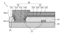
- FIG. 1 is a plan view showing an example of a wiring pattern of one wiring layer in a wiring body of a mounting substrate according to Embodiment 1.
- FIG. FIG. 2 is a cross-sectional view of the inter-via wiring portion of the mounting substrate taken along line II-II of FIG.
- FIG. 3 is a cross-sectional view of the interlayer connection portion of the mounting board taken along line III-III in FIG.
- FIG. 4 is a diagram for explaining a method of manufacturing a wiring transfer plate with wiring used when manufacturing the wiring body and the mounting substrate 1 according to the first embodiment.
- FIG. 5 is a diagram for explaining a method of manufacturing a wiring transfer plate.
- FIG. 6A is a cross-sectional view showing a modification of the wiring transfer plate.
- FIG. 6B is a cross-sectional view of an inter-via wiring portion of the mounting board according to the modification.
- FIG. 6C is a cross-sectional view of an interlayer connection portion of a mounting substrate according to a modification.
- FIG. 7 is a diagram showing a configuration when the wiring transfer plate with wiring produced in FIG. 4 is cut along another cross section.
- FIG. 8 is a diagram (cross-sectional view of a portion corresponding to the inter-via wiring portion in FIG. 2) for explaining the wiring body manufacturing method and the mounting substrate manufacturing method according to the first embodiment.
- FIG. 9 is a diagram (a cross-sectional view of a portion corresponding to the interlayer connection portion in FIG. 3) for explaining the wiring body manufacturing method and the mounting substrate manufacturing method according to the first embodiment.
- FIG. 10 is a cross-sectional view of a mounting board showing a first application example of the wiring body according to the first embodiment.
- FIG. 11 is a cross-sectional view of a mounting board showing a second application example of the wiring body according to the first embodiment.
- FIG. 12 is a cross-sectional view of a mounting substrate showing a third application example of the wiring body according to the first embodiment.
- 13 is a cross-sectional view of a mounting substrate according to Embodiment 2.
- FIG. 14A and 14B are diagrams for explaining the wiring body manufacturing method and the mounting board manufacturing method according to the second embodiment.
- FIG. 15 is a cross-sectional view of a mounting board according to the third embodiment.
- FIG. 16 is a diagram for explaining another example of the method of manufacturing the wiring transfer plate.
- each figure is a schematic diagram and is not necessarily strictly illustrated. Therefore, scales and the like are not always the same in each drawing. Moreover, in each figure, the same code
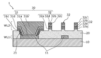
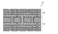
- FIG. 1 is a plan view showing an example of a wiring pattern of one wiring layer in a wiring body 30 of a mounting substrate 1 according to Embodiment 1.
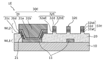
- FIG. FIG. 2 is a cross-sectional view of the inter-via wiring portion of the mounting substrate 1 along line II-II of FIG. 3 is a cross-sectional view of the interlayer connection portion of the mounting board 1 taken along line III--III in FIG.
- the mounting board 1 is, for example, a semiconductor package board, and has a plurality of wiring layers on which wiring is formed. Therefore, as shown in FIG. 1, the mounting substrate 1 includes, as the wiring bodies 30, via electrodes 31 for electrically connecting wiring between wiring layers, and wiring 32 which is wiring in one of the wiring layers. .
- the wiring 32 is connected to the via electrode 31 .
- the via electrode 31 is formed, for example, at the end of the portion where the wiring 32 extends, but it is not limited to this.
- the via electrode 31 may be formed in the middle of the wiring 32 .
- each wiring layer a plurality of via electrodes 31 and wirings 32 are formed.
- the mounting board 1 is a small ultra-high-density mounting board on which wirings 32 are mounted at high density.
- the mounting substrate 1 includes a substrate 10 and an insulating layer 20 and a wiring body 30 located on the substrate 10 .
- the wiring body 30 includes at least via electrodes 31 and wirings 32 as conductive members.
- the insulating layer 20 may be a part of the wiring body 30 .
- the substrate 10 has conductors 11 .
- the conductor 11 is, for example, a wiring or an electrode formed in a wiring layer different from the wiring 32 .
- the substrate 10 is a wiring board that is a board with wiring having wiring formed of copper foil or the like, and is, for example, a buildup board, a multilayer wiring board, a double-sided wiring board, or a single-sided wiring board. . Therefore, the substrate 10 is provided with a plurality of wirings or the like as the conductors 11 over a single layer or a plurality of layers. 2 and 3 schematically show only the conductors 11 formed on the outermost surface layer of the conductors 11 of the substrate 10. As shown in FIG.
- the mounting board 1 is an ultra-high-density mounting board
- the board 10 is a build-up board.
- the substrate 10 is not limited to a wiring substrate such as a build-up substrate, and may be an IC package substrate or an IC chip itself as long as it has wiring or electrodes as the conductor 11. good too.
- the insulating layer 20 is formed on the substrate 10 . Specifically, the insulating layer 20 covers the entire substrate 10 so as to cover the conductors 11 in the surface layer of the substrate 10 .
- the insulating layer 20 is arranged between the conductor 11 of the substrate 10 and the wiring 32 . Therefore, the insulating layer 20 is an interlayer insulating layer.
- the wiring layer in which the wiring that is the conductor 11 on the surface layer of the substrate 10 is formed is defined as the first wiring layer WL1, and the wiring 32 of the wiring body 30 is formed.
- the insulating layer 20 is an interlayer insulating layer between the first wiring layer WL1 and the second wiring layer WL2.
- a via hole 21 is formed in the insulating layer 20 .
- the via hole 21 is a through hole formed on the conductor 11 of the substrate 10 .
- a via electrode 31 is formed in the via hole 21 .
- the via hole 21 has a truncated cone shape with an inclined inner surface (tapered surface). Therefore, the opening shape (top view shape) of via hole 21 is circular, and the cross-sectional shape of via hole 21 is trapezoidal.
- the shape of the via hole 21 may be a truncated pyramid shape such as a quadrangular truncated pyramid shape, or may be a columnar shape or a prismatic shape.
- the insulating layer 20 is made of an insulating material.
- the insulating material forming the insulating layer 20 is, for example, an insulating resin.
- the insulating resin material for forming the insulating layer 20 may be a liquid insulating resin material having fluidity, which is composed of a photocurable resin such as an ultraviolet curable resin or a thermosetting resin.
- a prepreg made of a film-like insulating resin made of a thermosetting resin or a thermoplastic resin may also be used.
- An insulating resin sheet can be used as the film-like insulating resin. In this case, the insulating resin sheet preferably has adhesiveness.
- the insulating material forming the insulating layer 20 is not limited to an organic insulating material such as an insulating resin, and may be an inorganic insulating material such as a silicon oxide film or a silicon nitride film.
- the wiring body 30 is arranged on the substrate 10 having the conductor 11 .
- the via electrode 31 of the wiring body 30 is arranged on the conductor 11 of the substrate 10
- the wiring 32 of the wiring body 30 is arranged above the substrate 10 with the insulating layer 20 interposed therebetween.
- the wiring 32 is arranged on the insulating layer 20 . As shown in FIG. 2, the wiring 32 is arranged above the conductor 11 as the wiring of the substrate 10 with the insulating layer 20 interposed therebetween, but it is not limited to this.
- the wiring 32 is formed on the insulating layer 20 by a transfer method using a wiring transfer plate. It should be noted that the wiring 32 may not be entirely located on the surface of the insulating layer 20 , and the lower portion of the wiring 32 may be located within the insulating layer 20 .
- the via electrode 31 is connected to the conductor 11 of the substrate 10 through the via hole 21 of the insulating layer 20 .
- the via electrode 31 is a plug that connects upper and lower wirings sandwiching the insulating layer 20 .
- the via electrodes 31 are composed of wirings (conductors 11) of the first wiring layer WL1 located directly below the insulating layer 20 and wirings (wirings 32) of the second wiring layer WL2 located directly above the insulating layer 20. is connected to
- At least a part of the via electrode 31 is provided inside the via hole 21 .
- the via electrode 31 is embedded in the via hole 21 without gaps.
- the via electrode 31 is formed so as to protrude from the surface of the insulating layer 20 as well as inside the via hole 21 .
- the height of the via electrode 31 from the surface of the insulating layer 20 is higher than the height of the wiring 32 from the surface of the insulating layer 20 .
- the via electrode 31 is formed over the conductor 11 of the substrate 10 and over the insulating layer 20 .
- the via electrode 31 is formed so as to run over the surface of the insulating layer 20 from inside the via hole 21 of the insulating layer 20 . Therefore, the planar view area of the portion of the via electrode 31 protruding from the insulating layer 20 is larger than the maximum diameter area of the portion of the via electrode 31 embedded in the via hole 21 .
- the shape of the portion of the via electrode 31 embedded in the via hole 21 is the same as the shape of the via hole 21 . Therefore, in the present embodiment, the portion of the via electrode 31 embedded in the via hole 21 has a truncated cone shape with an inclined side surface (tapered surface). The minimum diameter of the portion of the via electrode 31 embedded in the via hole 21 is larger than the width of the wiring 32 .
- the via electrode 31 has a seed layer 31a, a via electrode body layer 31b provided on the seed layer 31a, and an adhesion layer 31c.
- the via electrode 31 further includes an electroless plated layer 31d between the adhesion layer 31c and the seed layer 31a. Note that the electroless plated layer 31d may be omitted.
- the seed layer 31 a is formed on the conductor 11 of the substrate 10 within the via hole 21 . Specifically, seed layer 31 a is formed on the upper surface of conductor 11 so as to be in contact with conductor 11 . The seed layer 31 a is formed along the inner surface of the insulating layer 20 from above the conductor 11 within the via hole 21 .
- the seed layer 31a is formed up to the main surface of the insulating layer 20 . That is, it is formed over the conductor 11 of the substrate 10 and over the main surface of the insulating layer 20 .
- the film thickness of the seed layer 31a is constant. Therefore, the seed layer 31 a is formed so as to extend over the main surface of the insulating layer 20 from the conductor 11 in the via hole 21 .
- the seed layer 31a is a seed electrode made of a conductive material for forming the via electrode body layer 31b by plating. Therefore, the seed layer 31a is preferably made of a conductive material with low electrical resistance.
- the seed layer 31a is a metal film made of a metal material containing copper, which is a low-resistance material, for example. In this case, the seed layer 31a may not be made of copper only, but may contain copper and other metal such as nickel. Note that the seed layer 31a may be a single film composed of only one metal film, or may be a laminated film in which a plurality of metal films are stacked.
- the via electrode body layer 31b is a plated film laminated on the seed layer 31a.
- via electrode body layer 31b is an electrolytic plated film formed by an electrolytic plating method.
- the via electrode body layer 31b is an electrolytic Cu-plated film made of copper.
- the via electrode body layer 31b is positioned on the seed layer 31a and is formed so as to fill the inside of the via hole 21 .
- the via electrode body layer 31b is formed up to the main surface of the insulating layer 20 .
- the via electrode body layer 31b is formed over the conductor 11 and the insulating layer 20 on the seed layer 31a.
- the via electrode body layer 31b is formed so as to run over the main surface of the insulating layer 20 from inside the via hole 21 of the insulating layer 20 .
- the via electrode body layer 31b constitutes most of the via electrode 31. In the present embodiment, via electrode body layer 31b occupies 90% or more of via electrode 31 in the cross-sectional view of FIG.
- the adhesion layer 31c is formed at least inside the via hole 21. Specifically, the adhesion layer 31 c is formed between the seed layer 31 a and the inner surface of the insulating layer 20 within the via hole 21 . The adhesion layer 31 c is sandwiched between the seed layer 31 a and the insulating layer 20 and contacts the seed layer 31 a and the insulating layer 20 . In the present embodiment, the adhesion layer 31c is formed over the main surface of the insulating layer 20, similarly to the seed layer 31a. Therefore, the adhesion layer 31 c is formed over the main surface of the insulating layer 20 and the position facing the inner side surface of the insulating layer 20 in the via hole 21 . The film thickness of the adhesion layer 31c is constant. Therefore, the adhesion layer 31 c is formed so as to run over the main surface of the insulating layer 20 from within the via hole 21 .
- the portion of the adhesion layer 31 c located above the insulating layer 20 is located between the insulating layer 20 and the portion of the via-electrode body layer 31 b located above the insulating layer 20 .
- an adhesion layer 31c, an electroless plated layer 31d, a seed layer 31a, and a via electrode body layer 31b are laminated in this order on the insulating layer 20.
- the adhesion layer 31 c is the lowest layer of the portion of the via electrode 31 located above the insulating layer 20 .
- the seed layer 31 a is the bottom layer of the via electrode 31 in the portion of the via electrode 31 inside the via hole 21 of the insulating layer 20 .
- the adhesion layer 31c (first adhesion layer) of the via electrode 31 is formed in the same layer as the adhesion layer 32a (second adhesion layer) of the wiring 32, which will be described later. That is, the adhesion layer 31c of the via electrode 31 and the adhesion layer 32a of the wiring 32 are made of the same material and formed in the same process.
- the electroless plated layer 31d is an electroless plated film formed by an electroless plating method. Specifically, the electroless plated layer 31d is an electroless Cu plated film made of copper. As described above, in the via electrode 31, the via electrode body layer 31b and the electroless plated layer 31d are both Cu plated films, and the electroless plated layer 31d is an electroless Cu plated film.
- the layer 31b is an electrolytic Cu plating film. Therefore, the via electrode body layer 31b and the electroless plated layer 31d contain copper with different crystal grain sizes.
- the average crystal grain size of copper forming the via-electrode body layer 31b which is an electrolytic Cu-plated film
- the average crystal grain size of copper forming the electroless-plated layer 31d is larger than the average crystal grain size of copper forming the electroless-plated layer 31d, which is an electroless-plated film.
- the average crystal grain size of copper forming the electroless plated layer 31d is smaller than the average crystal grain size of copper forming the via electrode body layer 31b, which is an electrolytic Cu plated film.
- the wiring 32 has an adhesion layer 32a provided as a lower layer of the wiring 32, and a wiring body layer 32b provided on the adhesion layer 32a.
- the adhesion layer 32 a is the bottom layer of the wiring 32 .
- the adhesion layer 32 a is provided on the main surface of the insulating layer 20 .
- the wiring 32 further has a conductive layer 32c provided on the wiring body layer 32b, and an electroless plated layer 32d provided between the adhesion layer 32a and the wiring body layer 32b. That is, the wiring 32 has a laminated structure in which the adhesion layer 32a, the electroless plated layer 32d, the wiring body layer 32b, and the conductive layer 32c are laminated in this order in the direction away from the insulating layer 20.
- FIG. The lower portion of the wiring body layer 32b and the adhesion layer 32a have the same line width.
- the adhesion layer 32a is provided to facilitate adhesion between the wiring 32 and the insulating layer 20.
- the adhesion layer 32 a has a function or structure for enhancing adhesion between the wiring 32 and the insulating layer 20 .
- the adhesion layer 32 a has a fine uneven structure as a structure for enhancing the adhesion between the wiring 32 and the insulating layer 20 .
- the adhesion layer 32a has a fine uneven structure as a whole layer, but it is not limited to this. 20 side. By providing the adhesion layer 32a having the fine uneven structure in this way, the adhesion layer 32a can be easily adhered to the insulating layer 20 by the anchor effect.
- Such a fine concavo-convex structure of the adhesion layer 32a is, for example, a needle-like concavo-convex shape with a height of 500 nm or less.
- the adhesion layer 32a is made of a metal film containing copper.
- the fine concavo-convex structure of the adhesion layer 32a is made of copper and/or copper oxide.
- a fine concave-convex structure can be formed by forming copper oxide having needle-like crystals on the copper surface and roughening the copper surface.
- the micro unevenness structure may be formed by slightly etching the copper surface by micro-roughening etching to roughen the surface.
- the adhesion layer 32a may be composed of a metal element other than copper.
- the adhesion layer 32a of the wiring 32 and the adhesion layer 31c of the via electrode 31 are formed in the same layer. That is, the adhesion layer 32a, which is the lower layer of the wiring 32, and the adhesion layer 31c, which is the lower layer of the via electrode 31 located on the insulating layer 20, are made of the same material and have the same fine uneven structure. Note that the adhesion layer 32a may be formed on the electroless plated layer 32d.
- the wiring body layer 32b is a plated film laminated under the conductive layer 32c.
- the wiring body layer 32b is an electroless plated film formed by an electroless plating method.
- the wiring body layer 32b is an electroless Cu plating film made of copper.
- the wiring body layer 32b of the wiring 32 and the via electrode body layer 31b of the via electrode 31 are both Cu-plated films, but the wiring body layer 32b is an electroless Cu-plated film, and the via electrode body layer 31b is an electroless Cu-plated film.
- 31b is an electrolytic Cu plating film. Therefore, the via electrode main layer 31b and the wiring main layer 32b contain copper with different crystal grain sizes. Specifically, the average crystal grain size of copper forming the via electrode main layer 31b, which is an electrolytic Cu-plated film, is larger than the average crystal grain size of copper forming the wiring main body layer 32b, which is an electroless plated film. In other words, the average crystal grain size of copper forming the wiring body layer 32b, which is an electroless plated film, is smaller than the average crystal grain size of copper forming the via electrode body layer 31b, which is an electrolytic Cu plated film.
- the via electrode body layer 31b as a relatively low-stress electrolytic plated film, it is possible to suppress the occurrence of plating peeling and cracks in the via electrode 31 due to internal stress. Further, by forming the wiring body layer 32b with an electroless plated film that can have a uniform film thickness, it is possible to easily form a plurality of wirings 32 having a large area and a uniform film thickness.
- Both the wiring body layer 32b of the wiring 32 and the via electrode body layer 31b of the via electrode 31 are plated films, but the wiring 32 does not have a seed layer as a lower layer. That is, the via electrode 31 has the seed layer 31a as its lower layer, but the wiring 32 does not have the seed layer as its lower layer.
- the wiring body layer 32b of the wiring 32 constitutes most of the wiring 32. In this embodiment, the wiring body layer 32b occupies 90% or more of the wiring 32 in the cross-sectional view of FIG.
- the conductive layer 32c formed on the wiring body layer 32b functions as a part of the conductor of the wiring 32 and also functions as a protective layer that protects the wiring body layer 32b. That is, when the seed layer 31a of the via electrode 31 is formed by etching and patterning the seed film, the conductive layer 32c can prevent the wiring body layer 32b from being etched and reduced. That is, the wiring body layer 32b can be protected by the conductive layer 32c when the seed film is etched. Thus, the conductive layer 32c functions as a protective layer that protects the wiring body layer 32b during etching.
- the conductive layer 32c is an electroless plated film like the wiring body layer 32b.
- the conductive layer 32c is composed of a material or structure different from that of the wiring body layer 32b.
- the conductive layer 32c is made of a conductive material different from that of the wiring body layer 32b.
- the conductive layer 32c is made of a conductive material other than copper.
- the conductive layer 32c is made of a material containing any one of nickel (Ni), palladium (Pd), platinum (Pt), and silver (Ag). That is, the conductive layer 32c is an electroless plated film containing any of these materials.
- the electroless plated layer 32d is an electroless plated film formed by an electroless plating method, like the wiring body layer 32b. Specifically, the electroless plated layer 32d is an electroless Cu plated film made of copper. However, the electroless plated film of the wiring body layer 32b and the electroless plated film of the electroless plated layer 32d are formed in separate steps.
- the electroless plated film of the wiring body layer 32b is of a type that is selectively deposited on the electrodes, and the electroless plated film of the electroless plated layer 32d can be formed uniformly over the entire surface of the insulating layer. is of type.
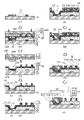
- FIG. 4A and 4B are diagrams for explaining a method of manufacturing the wiring transfer plate 200 with wiring used when manufacturing the wiring body 30 and the mounting substrate 1 according to the first embodiment.
- 5A and 5B are diagrams for explaining a method of manufacturing the wiring transfer plate 100.
- FIG. FIG. 6A is a cross-sectional view showing a modification of the wiring transfer plate.
- FIG. 6B is a cross-sectional view of an inter-via wiring portion of the mounting board according to the modification.
- FIG. 6C is a cross-sectional view of an interlayer connection portion of a mounting substrate according to a modification.
- FIG. 7 is a diagram showing a configuration when the wiring transfer plate 200 with wiring produced in FIG. 4 is cut along another cross section.
- 8 and 9 are diagrams for explaining the method for manufacturing the wiring body 30 and the method for manufacturing the mounting board 1 according to the first embodiment.
- 8 shows a method of manufacturing a portion corresponding to the inter-via wiring portion of FIG. 2
- FIG. 9 shows a method of manufacturing a portion corresponding to the interlayer connection portion of FIG.
- the wiring body 30 and the mounting substrate 1 are produced using the wiring transfer plate 100.
- the wiring transfer plate 100 is a wiring pattern plate for forming wiring (transfer wiring) to be transferred to another member (transfer target member) in a predetermined pattern.
- the wiring transfer plate 100 in the present embodiment is a plating pattern plate for forming an electroless plating film as transfer wiring.
- the electroless plated film formed by the wiring transfer plate 100 becomes at least part of the wiring to be transferred to another member.
- a method of manufacturing the wiring body 30 and the mounting board 1 using the wiring transfer plate 100 will be described below.
- a wiring transfer plate 200 with wiring is prepared in advance.
- the wiring transfer plate 200 with wiring is obtained by forming transfer wiring on the wiring transfer plate 100 .
- the wiring transfer plate 200 with wiring is the wiring transfer plate 100 on which the transfer wiring is formed.
- transfer wirings 36 for transferring to members constituting the mounting board 1 are formed.
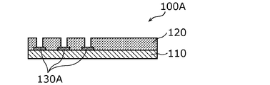
- a wiring transfer plate 100 is prepared.
- the wiring transfer plate 100 is prepared in advance as shown in FIG.
- a substrate with a plating base material is received, in which a plating base material layer 130 is formed on a base material 110 serving as a support substrate.
- a highly rigid substrate such as a glass substrate or a metal substrate is preferably used.
- a metal substrate made of SUS is used as base material 110 .
- the plating base material layer 130 is a catalyst base material layer for forming an electroless plating film.
- the plating base material constituting the plating base material layer 130 one or a plurality of materials selected from nickel (Ni), palladium (Pd), platinum (Pt), chromium (Cr), iron (Fe), etc. can be used.
- the plating base material layer 130 is a nickel film.
- an insulating layer 120 that will become a transfer plate insulating layer is formed on the plating base material layer 130 .
- the insulating layer 120 for example, a photoresist can be used.
- the insulating layer 120 which is a photoresist, is exposed and developed to form a plurality of openings 121 in the insulating layer 120, and the plating base material layer 130 is formed. expose the That is, the insulating layer 120 covers the base material 110 so as to have the opening 121 on the plating base material layer 130 .
- a protruding structure 140 is formed on the insulating layer 120 . Specifically, the protrusion structure 140 is formed on the insulating layer 120 . Thus, the wiring transfer plate 100 is completed.
- the protruding structures 140 formed on the insulating layer 120 are pillars for forming via holes for via electrodes in the insulating layer of the member (transferred member) to which the transfer wiring is transferred by the wiring transfer plate 100 .
- One or more protrusion structures 140 are formed according to the number of via holes to be formed.
- the protruding structure 140 is a protruding portion that protrudes from the main surface of the insulating layer 120 .
- the protrusion structure 140 is columnar. Since the projecting structure 140 is a projection for forming a via hole, it has the same shape as the via hole. In other words, the via hole has the same shape as the protrusion structure 140 . That is, the shape of the protrusion structure 140 is transferred to the insulating layer as the via hole.
- the protruding structure 140 has a truncated cone shape with an inclined side surface (tapered surface).
- the protruding structure 140 may have a truncated pyramid shape such as a truncated quadrangular pyramid shape, or may have a cylindrical shape, a prism shape, or the like.
- the side surface of the protrusion structure 140 does not have to be inclined with respect to the main surface of the insulating layer 120, but by making the side surface of the protrusion structure 140 an inclined surface, the transfer member can be insulated when the via hole is formed. The projecting structure 140 is easily removed from the layer.
- the protruding structure 140 may be made of either an organic material or an inorganic material, but preferably has a high rigidity that does not undergo plastic deformation.
- the protrusion structure 140 is made of an insulating resin material.
- the protrusion structure 140 is preferably made of a hard resin material.
- the protruding structure 140 may be made of a conductive resin material, or may be made of a material other than the resin material.
- the protrusion structure 140 may be made of a metal material, a ceramic material, or the like.
- the protrusion structure 140 may be made of the same material as the insulating layer 120 .
- the protrusion structure 140 may be formed integrally with the insulating layer 120 instead of being formed separately from the insulating layer 120 .
- the protruding structure 140 may be formed when exposing and developing the insulating layer 120 without providing the step (f) of FIG. .
- the plating base material layer 130 functions as a release layer. good too. Giving releasability to the plating base material layer 130 means weakening the catalytic reaction effect of the plating base material layer 130 .
- the plating base material layer 130 can be provided with releasability.
- the release treatment for the plating base material layer 130 is not limited to the oxidation treatment.
- the plating base material layer 130 is a continuous film in FIG. 5, it is not limited to this.
- the plating base material layer 130 may be patterned and separated to form the plating base material layer 130A for each opening 121.
- FIG. 5 is a continuous film in FIG. 5, it is not limited to this.
- the plating base material layer 130 may be patterned and separated to form the plating base material layer 130A for each opening 121.
- the transfer wiring 36 is formed on the wiring transfer plate 100 .
- an electroless plating film (electroless plating layer) is formed on the plating base material layer 130 by an electroless plating method.
- a metal is deposited and grown by a catalytic reaction caused by the catalyst of the plating base material layer 130 , thereby forming an electroless plating film on the plating base material layer 130 .
- a conductive layer 32c and a wiring body layer 32b made of different materials are laminated as electroless plating films.
- the plating base material layer 130 is a nickel film
- a conductive layer 32c made of an electrolytic pd-plated film is formed, and a wiring body layer 32b made of an electroless Cu-plated film is laminated on the conductive layer 32c.
- the conductive layer 32c is preferably an electroless plated film.
- the conductive layer 32c can be formed thin and with a uniform film thickness.
- the conductive layer 32c may be an electroplated film instead of an electroless plated film.
- the electroless Ni film or the electroless silver-plated film is removed without corroding Cu when forming a wiring body in a later step. Therefore, the wiring body can be easily made of only Cu. If the electroless Ni film remains, there is a concern that the wiring resistance of the wiring body will increase because the electroless Ni film generally contains substances such as boron and phosphorus and thus has high resistance. In addition, the electroless Ni film has magnetism, and there is a concern that the high-frequency characteristics and the like may be deteriorated. In addition, since silver is a metal that easily causes ion migration, there is a concern that reliability characteristics may deteriorate.
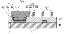
- FIG. 6B shows a cross-sectional view of the inter-via wiring portion of the mounting board corresponding to line II-II in FIG.
- FIG. 6C shows a cross-sectional view of the interlayer connection portion of the mounting board corresponding to line III-III in FIG.
- the conductive layer 32c remains at the connecting portion between the via electrode 31A and the wiring 32A. Good connection characteristics can be obtained as the seed layer 31a that forms the electrolytic Ni film or the electroless silver plating film and the electroless Cu film.
- the conductive layer 32c is an electroless Pd film or an electroless Pt film
- the electroless Pd film or the electroless Pt film generally contains almost no impurities, the surface resistance of the wiring can be kept low.
- it does not have magnetism, it is also advantageous in terms of high-frequency characteristics.
- Pd or Pt forming the electroless Pd film or the electroless Pt film is a metal that is more stable than Cu, it can function as a barrier layer that suppresses ion migration.
- the conductive layer 32c is preferably an electroless plated film.
- the film thickness of the conductive layer 32c can be formed to be uniform.
- the conductive layer 32c may be an electroplated film instead of an electroless plated film.
- an electroless plated film 33 is formed by an electroless plating method.
- an electroless Cu plating film is formed as the electroless plating film 33 .
- the electroless plated film 33 is formed not only on the metal but also on the insulating material. be.
- the electroless plated film 33 on the wiring body layer 32b is thinner than the electroless plated film on the insulating layer 120 because the electroless plated film 33 is difficult to self-grow on copper.
- an adhesion film 34 is formed.
- the adhesion film 34 covers at least the side surfaces of the protrusion structure 140 .
- the adhesion film 34 covers not only the side surfaces of the protruding structure 140 but also the upper surface thereof.
- the adhesion film 34 is formed on the entire surface of the insulating layer 120 so as to cover the protruding structure 140 and the electroless plated film 33 . That is, the adhesion film 34 is formed over the entire upper surface of the substrate 110 .
- the adhesion film 34 can be formed by forming a metal film such as a copper film made of copper over the entire upper surface of the base material 110 and performing an adhesion treatment for imparting adhesion to the metal film.
- the adhesion film 34 having a fine uneven structure can be formed by roughening the metal film as adhesion treatment.
- the conductive layer 32c, the wiring body layer 32b, the electroless plated film 33, and the adhesion film 34 constituting the transfer wiring 36 are formed on the wiring transfer plate 100.
- the attached wiring transfer plate 200 is completed.
- the wiring transfer plate 200 with wiring has a structure as shown in FIG.
- the wiring transfer plate 200 with wiring thus manufactured can transfer the transfer wiring 36 to another member. That is, the conductive layer 32c, the wiring body layer 32b, the electroless plated film 33, and the adhesion film 34 are the transfer wiring 36 to be transferred to another member.
- the wiring transfer plate 100 after transferring the transfer wirings 36 of the wiring transfer plate 200 with wires to another member returns to the state of (a) in FIG. 4 and can be used repeatedly. That is, the wiring transfer plate 100 can be reused. Specifically, as shown in (b) to (e) of FIG. It can be transferred to another member.
- the wiring body 30 and the mounting board 1 are manufactured by using the wiring transfer plate 200 with wiring. 8 showing the cross section of the inter-via wiring portion of the mounting board 1 and FIG. 9 showing the cross section of the interlayer connecting portion of the mounting board 1.
- FIG. 8 showing the cross section of the inter-via wiring portion of the mounting board 1
- FIG. 9 showing the cross section of the interlayer connecting portion of the mounting board 1.
- the transfer wiring 36 is arranged on the substrate 10 with the insulating layer 20 interposed therebetween.
- the transfer wiring 36 is formed by a transfer method using a wiring transfer plate 200 with wiring prepared in advance.
- a substrate 10 having conductors 11 is prepared.
- a build-up substrate is prepared in which wirings, electrodes, etc. are formed as conductors 11 on the uppermost layer.
- an insulating material is placed between the substrate 10 having the conductor 11 and the wiring transfer plate 200 with wiring, thereby separating the substrate 10 and the wiring.
- An insulating layer 20 is formed between the attached wiring transfer plate 200 and the wiring transfer plate 200 .
- an insulating material to be the insulating layer 20 is placed on the substrate 10 having the conductors 11, and the wiring transfer plate 200 with wires is placed on the insulating material. That is, the insulating material of the insulating layer 20 is inserted between the substrate 10 and the wiring transfer plate 200 with wiring. At this time, the wiring transfer plate 200 with wiring is arranged so that the transfer wiring 36 and the projecting structure 140 are on the insulating layer 20 side. In this case, the protrusion structure 140 is arranged so as to face the conductor 11 connecting the via electrode.
- the liquid insulating resin material is used as the insulating material for the insulating layer 20
- the liquid insulating resin material is applied onto the substrate 10 having the conductors 11, and the wiring transfer plate 200 with wiring is applied thereon. to cure the liquid insulating resin material.
- the liquid insulating resin material is a thermosetting resin
- it is cured by heating or drying
- the liquid insulating resin material is a photocurable resin
- the insulating layer 20 can be formed between the substrate 10 and the wiring transfer plate 200 with wiring in a state in which the protruding structures 140 are embedded in the insulating layer 20 .
- the film-like insulating resin sheet is placed on the substrate 10 having the conductors 11, and the wiring transfer plate 200 with wires is placed thereon. and heat-compress. At this time, since the wiring transfer plate 200 with wiring is pressed toward the substrate 10 , the portions of the insulating resin sheet corresponding to the projecting structures 140 are spread out by the projecting structures 140 . As a result, the insulating layer 20 can be formed between the substrate 10 and the wiring transfer plate 200 with wiring in a state in which the protruding structures 140 are embedded in the insulating layer 20 .
- the protrusion structure 140 of the wiring transfer plate 200 with wiring is arranged in the insulating material.
- the protrusion structure 140 is arranged in the insulating material so that the tip faces the conductor 11 with the adhesion film 34 interposed therebetween.
- the adhesion film 34 covering the upper surface of the protruding structure 140 is in contact with the conductor 11 .
- the protruding structure 140 is embedded in the insulating layer 20 in a state in which the tip is in contact with or close to the conductor 11 .
- a very thin insulating thin film 20a may exist partially or entirely between the adhesion film 34 covering the upper surface of the protruding structure 140 and the conductor 11 .
- the portion of the adhesion film 34 formed on the main surface of the insulating layer 120 of the wiring transfer plate 100 is formed on the upper surface of the insulating layer 20 .
- the wiring transfer plate 100 included in the wiring transfer plate 200 with wiring is separated from the insulating layer 20 . That is, the wiring transfer plate 100 and the insulating layer 20 are separated. As a result, the transfer wiring 36 of the wiring transfer plate 200 with wiring is separated from the plating base material layer 130 (release layer) and transferred to the substrate 10 side. Specifically, the transfer wiring 36 of the wiring transfer plate 200 with wiring is transferred to the insulating layer 20 , and the transfer wiring 36 is formed on the insulating layer 20 .
- the conductive layer 32c, the wiring body layer 32b, the electroless plated film 33, and the adhesion film 34 are transferred to the insulating layer 20. As shown in FIG.
- the insulating layer 20 in which the protruding structures 140 are embedded corresponds to the via hole 21 in the insulating layer 20 on the conductor 11.
- a recess 21a is formed. Recess 21 a is located above conductor 11 and is recessed from the main surface of insulating layer 20 .
- the recesses 21a corresponding to the via holes 21 are formed in the insulating layer 20 on the conductor 11, and the electroless plated film 33 and the adhesion film 34 form the insulating layer.
- the electroless plated film (conductive layer 32c, wiring body layer 32b) transferred to the inner side surface of the concave portion 21a of 20 and formed on the wiring transfer plate 200 with wiring is transferred to the insulating layer 20.
- FIG. Specifically, the electroless plated film 33 and the adhesion film 34 are transferred not only to the inner surface of the concave portion 21 a of the insulating layer 20 but also to the bottom surface.
- the transfer wiring 36 is easily separated from the plating base material layer 130, and the transfer wiring Since 36 has the adhesion film 34 , it is easily adhered to the insulating layer 20 . Thereby, the transfer wiring 36 can be easily transferred to the insulating layer 20 .
- the laminated wiring of the conductive layer 32 c and the wiring body layer 32 b , the electroless plated film 33 and the adhesion film 34 can be easily transferred to the insulating layer 20 .
- the insulating resin sheet when a film-shaped insulating resin sheet is used as the insulating material for the insulating layer 20, the insulating resin sheet preferably has adhesiveness. This makes it easier for the adhesion film 34 of the transfer wiring 36 to adhere to the insulating layer 20 , so that the transfer wiring 36 can be transferred to the insulating layer 20 more easily.
- the member in which the transfer wiring 36 is transferred by the wiring transfer plate 200 with wiring and the concave portion 21 a is formed in the insulating layer 20 is an intermediate member of the wiring body 30 arranged on the substrate 10 . It is an intermediate body material 300 . Therefore, the wiring body intermediate material 300 is positioned on the substrate 10, and includes the insulating layer 20 having the recess 21a, the adhesion film 34 formed on the inner side surface and the bottom surface of the recess 21a, and the insulating layer 20, and the adhesive film 34 is formed on the insulating layer 20. A laminate (laminated wiring) of a conductive layer 32c functioning as a wiring located on the film 34 and a wiring body layer 32b is provided. Intermediate material 300 for a wiring body in the present embodiment is formed using wiring transfer plate 200 with wiring, and concave portions 21a are formed by projecting structures 140 in wiring transfer plate 200 with wiring.
- the electroless plated film 33 and the adhesion film 34 existing on the conductor 11 are removed.
- the residue of the insulating material of the insulating layer 20 inside the via hole 21 is also removed.
- the insulating thin film 20a remaining on the conductor 11 as a residue of the insulating material of the insulating layer 20 is also removed.
- the electroless plated film 33 and the adhesion film 34 on the conductor 11 and the residue of the insulating material may be removed by laser patterning or by etching. It may be removed by dry or wet ashing.
- the wiring body intermediate material 300 may be obtained by performing this removing process.
- a seed film 35 is formed so as to cover the exposed conductor 11, the electroless plated film, and the wiring body layer 32b. Specifically, after removing the residue of the insulating layer 20 by desmearing and laser processing, the seed film 35 is formed over the entire upper surface of the substrate 10 by electroless plating or sputtering. Further, in the present embodiment, since the conductive layer 32c exists on the wiring body layer 32b, the seed film 35 is laminated on each of the conductor 11, the electroless plated film 33 and the conductive layer 32c.
- the seed film 35 is a seed electrode for forming the via electrode body layer 31b of the via electrode 31 by electroplating. Therefore, the wiring body layer 32b and the conductive layer 32c can be protected by the seed film 35 until the seed film 35 is removed in subsequent steps.
- the seed film 35 covers not only the upper portion of the conductive layer 32c but also the side portions of the wiring body layer 32b and the conductive layer 32c. Therefore, a small amount of the seed film 35 component (such as Pd) is present on the top and side portions of the wiring body layer 32b and the conductive layer 32c.
- the seed film 35 is a metal film made of a metal material containing copper.
- the seed film 35 may consist of only copper, or may contain copper and other metals such as nickel.
- a resist 40 is selectively formed on the seed film 35 so that the portion of the seed film 35 covering the conductor 11 is exposed. . Specifically, an opening 41 is formed in the resist 40 above the conductor 11 .
- the resist 40 covers the wiring body layer 32b.
- a dry film resist (DFR), for example, can be used as the resist 40 .
- the via electrode body layer 31b is formed on the exposed seed film 35. Then, as shown in FIG. Specifically, the via electrode body layer 31b is formed so as to fill the inside of the opening 41 of the resist 40 .
- an electrolytic plated film is formed on the seed film 35 in the opening 41 by an electrolytic plating method as the via electrode main body layer 31b.
- the via electrode body layer 31b is an electrolytic Cu plating film.
- part of the via electrode body layer 31b is formed on the end of the transfer wiring 36 in the interlayer connection. Specifically, part of the via electrode body layer 31 b is formed on the seed film 35 laminated on the transfer wiring 36 .
- the resist 40 is removed. Specifically, the resist 40, which is a dry film resist, is removed. As a result, the portion of the seed film 35 covered with the resist 40 is exposed.
- the exposed seed film 35 is removed, and the electroless plated film 33 and the adhesion film existing under the exposed seed film 35 are removed.
- 34 is removed. That is, the portion of the seed film 35 that covers the wiring body layer 32b is removed, and the portions of the electroless plated film 33 and the adhesion film 34 that are not covered with the wiring body layer 32b and the via electrode body layer 31b are removed.
- the exposed seed film 35 and the electroless plated film 33 and adhesion film 34 existing under the exposed seed film 35 are removed by etching using an etchant.
- the seed film 35 and the conductive layer 32c of the transfer wiring 36 are made of different conductive materials, the seed film 35 can be selectively etched without etching the conductive layer 32c. As a result, undercutting of the lower layer of the transfer wiring 36 due to this etching can be suppressed, so that reduction of the line width of the lower layer of the wiring 32 can be suppressed.
- the seed film 35, the electroless plated film 33, and the adhesion film 34 remain under the via electrode body layer 31b.
- the remaining seed film 35 becomes the seed layer 31a
- the remaining electroless plating film 33 becomes the electroless plating layer 31d
- the remaining adhesion film 34 becomes the adhesion layer 31c.
- the seed film 35, the electroless plating film 33 and the adhesion film 34 are etched so that the electroless plating film 33 and the adhesion film 34 remain under the wiring body layer 32b.
- the remaining electroless plating film 33 becomes the electroless plating layer 32d, and the remaining adhesion film 34 becomes the adhesion layer 32a. and wiring 32 is formed.
- the electroless plated film 33 laminated on the wiring body layer 32b is thinner than the electroless plated film laminated on the insulating layer 120, so the thickness of the electroless plated layer 32d in the wiring 32 is The thickness is thinner than the thickness of the electroless plated layer 31 d in the via electrode 31 . In other words, the thickness of the electroless plated layer 31 d in the via electrode 31 is thicker than the thickness of the electroless plated layer 32 d in the wiring 32 .
- the wiring bodies 30 having the via electrodes 31 and the wirings 32 are formed, and the mounting substrate 1 having the wiring bodies 30 can be produced. That is, the wiring body 30 can be manufactured on the substrate 10 having the conductor 11 , and the mounting substrate 1 with the wiring body 30 arranged on the substrate 10 can be manufactured.
- the wiring 32 of the wiring body 30 is formed by the transfer method. Specifically, the wiring 32 is formed using the wiring transfer plate 100 .
- the fine wiring 32 can be formed with high accuracy.
- the wiring is formed by the photolithography method, if the surface of the portion where the wiring is formed has unevenness, the focus is shifted and the fine wiring cannot be formed with high precision.
- the wiring transfer plate 100 by transferring and forming the wiring 32 using the wiring transfer plate 100, even if the surface of the portion where the wiring 32 is formed has unevenness and the flatness is not good, the unevenness can be absorbed. can be formed, and fine wiring 32 can be formed with high accuracy.
- the wiring 32 can be formed with high alignment accuracy.
- the wiring transfer plate 200 with the wiring in which the transfer wiring 36 is formed on the wiring transfer plate 100 having the projection structure 140 is used.
- the wiring transfer plate 200 with wiring includes, as the transfer wiring 36, the adhesion film 34 covering at least the side surface of the protrusion structure 140 of the wiring transfer plate 100, and the laminated wiring of the conductive layer 32c and the wiring body layer 32b.
- the protrusion structure 140 of the wiring transfer plate 200 with wiring is arranged in an insulating material, and by separating the wiring transfer plate 100, the conductor A recessed portion 21a corresponding to the via hole 21 is formed in the portion of the insulating layer 20 on the 11, and the adhesion film 34 is transferred to the inner surface of the recessed portion 21a of the insulating layer 20 and formed on the wiring transfer plate 200 with wiring.
- the conductive layer 32c and the wiring body layer 32b, which are plated films, are transferred to the insulating layer 20. Then, as shown in FIG.
- the wiring transfer plate 100 according to the present embodiment includes the protrusion structure 140 having the adhesion film 34 formed on at least the side surface thereof, the wiring transfer plate 200 having the wiring transfer plate 100 is used.
- the recess 21a for the via electrode 31 and the adhesion film 34 can be formed on the substrate 10 at the same time.
- the recess 21a having the adhesive film 34 formed on the inner surface can be formed in the insulating layer 20 at the same time. Adhesion with the layer 20 can be improved.
- the via electrode body layer 31b which is a plating film, on the seed layer 31a to form the via electrode 31, it is possible to obtain the wiring body 30 and the mounting substrate 1 having the highly reliable via electrode 31. .
- the adhesion film 34 in the wiring transfer plate 200 with wiring in the present embodiment is formed on the insulating layer 120 of the wiring transfer plate 100 so as to cover the protrusion structure 140 and the laminated wiring of the conductive layer 32c and the wiring body layer 32b. formed.
- the concave portion 21 a having the adhesion film 34 formed on the inner surface is formed in the insulating layer 20 .
- the adhesion film 34, and the conductive layer 32c and the wiring body layer 32b as the wiring positioned on the adhesion film 34 are transferred.
- the wiring body intermediate member 300 in which the concave portion 21a having the adhesion film 34 formed on the inner surface thereof and the wiring (the conductive layer 32c and the wiring body layer 32b) on the insulating layer 20 are simultaneously formed.
- the wiring body 30 and the mounting substrate 1 according to the present embodiment manufactured in this way are provided in the via holes 21 formed in the insulating layer 20 located on the substrate 10, and are mounted through the via holes 21.
- a via electrode 31 connected to the conductor 11 and a wiring 32 provided above the substrate 10 via the insulating layer 20 are provided.
- the adhesion layer 31 c is interposed between the seed layer 31 a and the insulating layer 20 on the lateral side of the via hole 21 . That is, in the via hole 21, the seed layer 31a and the insulating layer 20 are adhered to each other through the adhesion layer 31c.
- the adhesion layer 31c in this way, the adhesion between the seed layer 31a and the insulating layer 20 can be improved. Therefore, it is possible to obtain the wiring body 30 and the mounting substrate 1 having the via electrodes 31 with high reliability.
- the adhesion layer 31c of the via electrode 31 is formed on the main surface of the insulating layer 20 as well.
- the adhesion layer 31c is formed not only in the via hole 21 but also on the main surface of the insulating layer 20 .
- the adhesion layer 31c can be brought into close contact with the insulating layer 20 even on the insulating layer 20 .
- the adhesion between the seed layer 31a and the insulating layer 20 is further improved, so that the reliability of the via electrode 31 is further improved.
- the seed layer 31a and the via electrode main layer 31b are formed on the main surface of the insulating layer 20, and the adhesion layer 31c of the via electrode 31 is The portion located above the insulating layer 20 is located between the portion located above the insulating layer 20 and the insulating layer 20 in the via-electrode body layer 31b.
- the seed layer 31a and the insulating layer 20 can be adhered to each other even on the insulating layer 20 via the adhesion layer 31c. Thereby, the adhesion between the seed layer 31a and the insulating layer 20 can be greatly improved. Therefore, it is possible to realize the wiring body 30 and the mounting board 1 having the via electrodes 31 with higher reliability.
- the adhesion layer 31c of the via electrode 31 has a fine uneven structure.
- the adhesion layer 31c can easily adhere to the insulating layer 20 and the seed layer 31a due to the anchor effect. Thereby, the adhesion between the seed layer 31a and the insulating layer 20 is further improved.
- the line width of the wiring 32 in the present embodiment is preferably 5 ⁇ m or less, more preferably 2 ⁇ m or less.
- the wiring 32 is preferably 5 ⁇ m or less, more preferably 2 ⁇ m or less.
- the wiring body 30 manufactured in this manner can be used as a wiring layer or a redistribution layer (RDL) in a semiconductor package substrate.
- RDL redistribution layer
- the wiring body 30 can be used as a rewiring layer in a mounting substrate 1A, which is a 2.1D semiconductor package substrate (organic interposer).
- a rewiring layer in the mounting substrate 1B which is a 2.3D semiconductor package substrate (organic interposer).
- the substrate 10 is a buildup substrate.
- the wiring body 30 can be used as a rewiring layer in the mounting substrate 1C, which is a 2.5D semiconductor package substrate (Si or Glass interposer).
- the wiring body 30 can also be used as a rewiring layer in a mounting board that is an FO-WLP (Fan Out-Wafer Level Package).
- FO-WLP Full Out-Wafer Level Package
- the mounting substrates 1A, 1B, and 1C shown in FIGS. 10 to 12 can also be applied to the following second and third embodiments.
- the wiring body 30 can also be applied to the buildup layer (wiring layer) itself of a general buildup board instead of the rewiring layer.
- the wiring body 30 can be applied to the wiring layer of the board 10, which is a buildup board shown in FIGS. 11 to 13. FIG.
- the wiring distance from the electronic component formed in the core such as an inductor or capacitor to the semiconductor is shortened, so the electrical characteristics are improved, and an interposer or rewiring layer is not required. Therefore, an inexpensive semiconductor package can be obtained.
- FIG. 13 is a cross-sectional view of a mounting board 1D according to the second embodiment.
- the wiring 32 in the first embodiment has the conductive layer 32c formed on the wiring body layer 32b, as shown in FIG. 2, the conductive layer 32c is not formed on the wiring body layer 32b.
- the wiring 32D is composed only of the adhesion layer 32a, the electroless plated layer 32d, and the wiring body layer 32b.
- the seed layer 31a of the via electrode 31 and the wiring body layer 32b of the wiring 32 contain the same metal.
- seed layer 31aD of via electrode 31D and wiring body layer 32b of wiring 32D contain different kinds of metals.
- both the seed layer 31a and the wiring body layer 32b are metal films containing copper, but in the present embodiment, the wiring body layer 32b is composed only of copper.
- the seed layer 31aD is a metal film containing a metal other than copper. That is, in the present embodiment, the wiring body layer 32b of the wiring 32D is the same as that of the first embodiment, but the seed layer 31aD of the via electrode 31D is different from that of the first embodiment and is made of a metal other than copper. contains.
- the wiring body 30D and the mounting structure according to the present embodiment are the same.
- the substrate 1D is the same as the wiring body 30 and the mounting substrate 1 according to the first embodiment.
- the wiring body 30D and mounting board 1D configured in this manner are manufactured by the method shown in FIG. 14A and 14B are diagrams for explaining a method for manufacturing the wiring body 30D and a method for manufacturing the mounting board 1D according to the second embodiment.
- a wiring transfer plate 200D with wiring is used in which transfer wirings 36D are formed on the wiring transfer plate 100 having the projecting structures 140.
- the wiring 32D is formed by the transfer method using the wiring transfer plate 200D with the wiring prepared in advance.
- the transfer wiring 36D does not have the conductive layer 32c.
- the transfer wiring 36D is composed of the wiring body layer 32b, the electroless plated film 33, and the adhesion film .
- transfer wiring 36D is arranged on substrate 10 with insulating layer 20 interposed therebetween.
- a substrate 10 having conductors 11 is prepared in the same manner as in the step of FIG. 8(a).
- an insulating material is placed between the substrate 10 having the conductors 11 and the wiring transfer plate 200D with wiring, similarly to the step of FIG. 8(b).
- the insulating layer 20 is formed between the substrate 10 and the wiring transfer plate 200D.
- the wiring transfer plate 100 included in the wiring transfer plate 200D with wiring is separated from the insulating layer 20 in the same manner as in the step of FIG. 8(c).
- the transfer wiring 36D of the wiring transfer plate 200D with wiring is separated from the plating base material layer 130 and transferred to the substrate 10 side.
- the transfer wiring 36 ⁇ /b>D of the wiring transfer plate 200 ⁇ /b>D with wiring is transferred to the insulating layer 20 and formed on the insulating layer 20 .
- the wiring body layer 32b, the electroless plated film 33, and the adhesion film 34 are transferred to the insulating layer 20.
- FIG. 14(c) the wiring transfer plate 100 included in the wiring transfer plate 200D with wiring is separated from the insulating layer 20 in the same manner as in the step of FIG. 8(c).
- the insulating layer 20 in which the protruding structures 140 are embedded corresponds to the via hole 21 in the insulating layer 20 on the conductor 11.
- a recess 21a is formed. That is, also in this embodiment, the recess 21a for the via electrode 31D and the wiring 32D can be formed on the substrate 10 at the same time.
- the electroless plated film 33 and the adhesion film 34 on the conductor 11 are removed in the same manner as in the step of FIG. 8(d).
- the residue of the insulating material of the insulating layer 20 may be removed together with the electroless plated film 33 and the adhesion film 34 in this embodiment as well.
- the insulating thin film 20a remaining on the conductor 11 as a residue of the insulating material of the insulating layer 20 is removed.
- a seed film is formed so as to cover the exposed conductor 11, the electroless plated film 33, and the wiring body layer 32b in the same manner as in the step (e) of FIG. Form 35D.
- a seed film 35 ⁇ /b>D is formed over the entire upper surface of the substrate 10 .
- the seed film 35D contains a different kind of metal than the wiring body layer 32b.
- the wiring body layer 32b is composed only of copper, but the seed film 35D contains a metal other than copper.
- the seed film 35D is selectively deposited on the seed film 35D so that the portion of the seed film 35D covering the conductor 11 is exposed.
- a resist 40 is formed.
- the via electrode body layer 31b is formed on the exposed seed film 35D in the same manner as in the step (g) of FIG. Specifically, the via electrode body layer 31b is formed so as to fill the inside of the opening 41 of the resist 40 .
- the via electrode body layer 31b is an electroplated film laminated on the seed film 35D of the opening 41 by electroplating.
- the via electrode body layer 31b is an electrolytic Cu plating film.
- the resist 40 is removed in the same manner as in the step of FIG. 8(h). As a result, the portion of the seed film 35D covered with the resist 40 is exposed.
- the film 34 is removed by etching using an etchant. That is, the portion of the seed film 35D that covers the wiring body layer 32b is removed, and the electroless plated film 33 and the adhesion film 34 that are not covered with the wiring body layer 32b and the via electrode body layer 31b are removed.
- the wiring body layer 32b of the transfer wiring 36D contains a metal different from that of the seed film 35D. 31c are formed, and wiring 32D having an adhesion layer 32a, an electroless plated layer 31d, and a wiring body layer 32b is formed.
- the wiring body 30D having the via electrode 31D and the wiring 32D is formed, and the mounting substrate 1D having the wiring body 30D can be manufactured. That is, the wiring body 30D can be manufactured on the substrate 10 having the conductor 11, and the mounting board 1D having the wiring body 30D arranged on the substrate 10 can be manufactured.
- the adhesion layer 31c is formed between the seed layer 31aD and the inner surface of the insulating layer 20 within the via hole 21 .
- the adhesion between the seed layer 31aD and the insulating layer 20 is improved, so that it is possible to obtain the via electrode 31D with high reliability.
- the wiring 32D does not have the conductive layer 32c in the present embodiment, the wiring 32D may have the conductive layer 32c.
- FIG. 15 is a cross-sectional view of a mounting board 1E according to the third embodiment.
- the wiring 32 includes an adhesion layer 32a having a fine uneven structure, an electroless plating layer 32d (seed layer) that is an electroless plating film of Cu, and a wiring main body that is an electroless plating film of Cu.
- an adhesion layer 32a having a fine uneven structure an electroless plating layer 32d (seed layer) that is an electroless plating film of Cu
- a wiring main body that is an electroless plating film of Cu.
- the present invention is not limited to this.
- the wiring 32E does not have the conductive layer 32c as a protective layer, and the adhesion layer 32aE and It is composed of an electroless plated layer 32d and a wiring body layer 32bE.
- the adhesion layer 32aE does not form a micro uneven structure by copper oxide treatment or the like, but is formed by forming an organic thin film by organic adhesion treatment.
- the adhesive layer 32aE is chemically bonded to the resin forming the insulating layer 20. It is possible to form an organic thin film composed of an organic component and an organic component chemically bonded to copper constituting the wiring body layer 32bE.
- the adhesion layer 32a is formed by copper oxide treatment, there is a possibility that the electroless plated layer 32d (seed layer) may be peeled off during the copper oxide treatment, or the wiring 32 may be peeled off during etching because copper oxide is vulnerable to acid.
- the adhesion layer 32aE by forming the adhesion layer 32aE by an organic adhesion process as in the present embodiment, such a problem can be suppressed.
- the wiring body layer 32bE is not an electroless plated film but an electroplated film.
- the wiring body layer 32bE is an electroplating film made of copper. Accordingly, since there is etching selectivity between the wiring body layer 32bE, which is an electroplating film, and the electroless plating layer 32d, which is an electroless plating film, the conductive layer 32c as a protective layer as in the first embodiment is unnecessary. Become.
- the wiring body 30E and the mounting board 1E according to the present embodiment are the same as the wiring body 30 and the mounting board 1 according to the first embodiment except for the configuration of the wiring 32E. Moreover, this embodiment can be applied not only to the first embodiment but also to the second embodiment.
- the insulating layer 120 serving as the transfer plate insulating layer in the wiring transfer plate 100 is a resist, but the present invention is not limited to this.
- the insulating layer 120 may be an insulating resin material made of an inorganic material such as SiO2 .
- the wiring transfer plate 100B having the insulating layer 120B can be manufactured by the method shown in FIG.
- a substrate with a plating base material is received, which is a base material 110 serving as a support substrate and a plating base material layer 130 formed thereon.
- an insulating layer 120B (transfer plate insulating layer) made of SiO 2 is formed on the plating base material layer 130 .
- a resist 150 is formed on the insulating layer 120.
- the resist 150 is patterned by exposing and developing the resist 150 to form an opening 151 in the resist 150 and expose the insulating layer 120 .
- the electroless plated film may be an electroplated film, and the electroplated film may be an electrolytic plated film.
- the electroless plated film and the electroplated film may be plated films without distinction.
- a wiring body according to the present disclosure is useful as a wiring layer or the like in a mounting substrate such as a semiconductor package substrate.
Landscapes
- Engineering & Computer Science (AREA)
- Manufacturing & Machinery (AREA)
- Microelectronics & Electronic Packaging (AREA)
- Manufacturing Of Printed Wiring (AREA)
- Physics & Mathematics (AREA)
- Geometry (AREA)
- Ceramic Engineering (AREA)
Priority Applications (3)
| Application Number | Priority Date | Filing Date | Title |
|---|---|---|---|
| JP2023509074A JPWO2022202553A1 (https=) | 2021-03-22 | 2022-03-16 | |
| EP22775341.5A EP4319510A4 (en) | 2021-03-22 | 2022-03-16 | WIRING BODY, MOUNTING SUBSTRATE, WIRING TRANSFER BOARD WITH WIRING, INTERMEDIATE MATERIAL FOR WIRING BODY, AND METHOD FOR MANUFACTURING WIRING BODY |
| US18/548,450 US20240145374A1 (en) | 2021-03-22 | 2022-03-16 | Wiring body, mounting substrate, wiring-equipped wiring transfer plate, wiring body intermediate material, and method for manufacturing wiring body |
Applications Claiming Priority (2)
| Application Number | Priority Date | Filing Date | Title |
|---|---|---|---|
| JP2021047463 | 2021-03-22 | ||
| JP2021-047463 | 2021-03-22 |
Publications (1)
| Publication Number | Publication Date |
|---|---|
| WO2022202553A1 true WO2022202553A1 (ja) | 2022-09-29 |
Family
ID=83396159
Family Applications (1)
| Application Number | Title | Priority Date | Filing Date |
|---|---|---|---|
| PCT/JP2022/011952 Ceased WO2022202553A1 (ja) | 2021-03-22 | 2022-03-16 | 配線体、実装基板、配線付き配線転写版、配線体用中間材、及び、配線体の製造方法 |
Country Status (4)
| Country | Link |
|---|---|
| US (1) | US20240145374A1 (https=) |
| EP (1) | EP4319510A4 (https=) |
| JP (1) | JPWO2022202553A1 (https=) |
| WO (1) | WO2022202553A1 (https=) |
Families Citing this family (2)
| Publication number | Priority date | Publication date | Assignee | Title |
|---|---|---|---|---|
| US12414231B2 (en) * | 2022-03-29 | 2025-09-09 | Ibiden Co., Ltd. | Printed wiring board |
| JP2024172826A (ja) * | 2023-06-01 | 2024-12-12 | イビデン株式会社 | プリント配線板 |
Citations (6)
| Publication number | Priority date | Publication date | Assignee | Title |
|---|---|---|---|---|
| JPH11112126A (ja) * | 1997-10-06 | 1999-04-23 | Matsushita Electric Ind Co Ltd | 微細パターンの製造方法 |
| US20080052905A1 (en) * | 2006-09-06 | 2008-03-06 | Samsung Electro-Mechanics Co., Ltd. | Fabricating method for printed circuit board |
| JP2009221498A (ja) * | 2008-03-13 | 2009-10-01 | Seiko Epson Corp | めっき膜、めっき膜の製造方法、配線基板、配線基板の製造方法 |
| WO2011058978A1 (ja) * | 2009-11-10 | 2011-05-19 | 株式会社フジクラ | 配線基板の製造方法 |
| JP2017073530A (ja) * | 2015-10-09 | 2017-04-13 | 富士通株式会社 | 密着性向上材料、配線構造、及びその製造方法、並びに半導体装置、及びその製造方法 |
| JP2020107681A (ja) | 2018-12-26 | 2020-07-09 | 新光電気工業株式会社 | 配線基板、半導体装置、及び配線基板の製造方法 |
Family Cites Families (9)
| Publication number | Priority date | Publication date | Assignee | Title |
|---|---|---|---|---|
| MY139405A (en) * | 1998-09-28 | 2009-09-30 | Ibiden Co Ltd | Printed circuit board and method for its production |
| JPWO2003032701A1 (ja) * | 2001-09-28 | 2005-01-27 | 富士通株式会社 | 多層配線基板の製造方法およびこれにより製造される多層配線基板 |
| US20040251548A1 (en) * | 2003-06-16 | 2004-12-16 | United Microelectronics Corp. | Method for forming barrier layer and structure |
| JP5113544B2 (ja) * | 2008-01-30 | 2013-01-09 | 新光電気工業株式会社 | 配線基板の製造方法 |
| KR101152822B1 (ko) * | 2009-07-31 | 2012-06-12 | 에스케이하이닉스 주식회사 | 웨이퍼의 형성방법 |
| JP5436995B2 (ja) * | 2009-09-14 | 2014-03-05 | 新光電気工業株式会社 | 配線基板及びその製造方法 |
| JP5602584B2 (ja) * | 2010-10-28 | 2014-10-08 | 新光電気工業株式会社 | 配線基板及びその製造方法 |
| JP2012216773A (ja) * | 2011-03-29 | 2012-11-08 | Shinko Electric Ind Co Ltd | 配線基板及びその製造方法 |
| JP6324876B2 (ja) * | 2014-07-16 | 2018-05-16 | 新光電気工業株式会社 | 配線基板、半導体装置及び配線基板の製造方法 |
-
2022
- 2022-03-16 JP JP2023509074A patent/JPWO2022202553A1/ja not_active Withdrawn
- 2022-03-16 EP EP22775341.5A patent/EP4319510A4/en not_active Withdrawn
- 2022-03-16 US US18/548,450 patent/US20240145374A1/en active Pending
- 2022-03-16 WO PCT/JP2022/011952 patent/WO2022202553A1/ja not_active Ceased
Patent Citations (6)
| Publication number | Priority date | Publication date | Assignee | Title |
|---|---|---|---|---|
| JPH11112126A (ja) * | 1997-10-06 | 1999-04-23 | Matsushita Electric Ind Co Ltd | 微細パターンの製造方法 |
| US20080052905A1 (en) * | 2006-09-06 | 2008-03-06 | Samsung Electro-Mechanics Co., Ltd. | Fabricating method for printed circuit board |
| JP2009221498A (ja) * | 2008-03-13 | 2009-10-01 | Seiko Epson Corp | めっき膜、めっき膜の製造方法、配線基板、配線基板の製造方法 |
| WO2011058978A1 (ja) * | 2009-11-10 | 2011-05-19 | 株式会社フジクラ | 配線基板の製造方法 |
| JP2017073530A (ja) * | 2015-10-09 | 2017-04-13 | 富士通株式会社 | 密着性向上材料、配線構造、及びその製造方法、並びに半導体装置、及びその製造方法 |
| JP2020107681A (ja) | 2018-12-26 | 2020-07-09 | 新光電気工業株式会社 | 配線基板、半導体装置、及び配線基板の製造方法 |
Non-Patent Citations (1)
| Title |
|---|
| See also references of EP4319510A4 |
Also Published As
| Publication number | Publication date |
|---|---|
| EP4319510A1 (en) | 2024-02-07 |
| EP4319510A4 (en) | 2024-10-02 |
| US20240145374A1 (en) | 2024-05-02 |
| JPWO2022202553A1 (https=) | 2022-09-29 |
Similar Documents
| Publication | Publication Date | Title |
|---|---|---|
| KR101103857B1 (ko) | 인쇄 배선 보드 및 그 제조 방법 | |
| CN110890320A (zh) | 半导体封装件及其制造方法 | |
| US9455219B2 (en) | Wiring substrate and method of manufacturing the same | |
| JP5300558B2 (ja) | 半導体装置の製造方法 | |
| US10777495B2 (en) | Printed circuit board and semiconductor package including the same | |
| WO2022202548A1 (ja) | 配線体、実装基板、配線付き配線転写版、配線体用中間材、配線体の製造方法、及び、実装基板の製造方法 | |
| TW200921876A (en) | Method for making copper-core layer multi-layer encapsulation substrate | |
| TW200303609A (en) | Semiconductor device and manufacturing method thereof | |
| CN104377187B (zh) | Ic载板、具有该ic载板的半导体器件及制作方法 | |
| CN104247584A (zh) | 印刷电路板及其制造方法 | |
| WO2022202553A1 (ja) | 配線体、実装基板、配線付き配線転写版、配線体用中間材、及び、配線体の製造方法 | |
| CN108701660B (zh) | 半导体封装衬底及其制造方法 | |
| JP2007324559A (ja) | ファインピッチを有するマルチレイヤー回路板及びその製作方法 | |
| JPH0536756A (ja) | 半導体装置用テープキヤリア及びその製造方法 | |
| CN102111954A (zh) | 线路板及其制作工艺 | |
| US10874018B2 (en) | Printed wiring board having embedded pads and method for manufacturing the same | |
| WO2008007617A1 (en) | Electrode connection structure of semiconductor chip, conductive member, and semiconductor device and method for manufacturing the same | |
| WO2022202552A1 (ja) | 配線転写版、配線付き配線転写版、配線体用中間材、及び、配線体の製造方法 | |
| WO2021253574A1 (zh) | 多层基板及其制作方法 | |
| WO2022202547A1 (ja) | 配線体、実装基板、配線体の製造方法、及び、実装基板の製造方法 | |
| KR101272664B1 (ko) | 시드층 및 도금층을 포함하는 금속 패턴을 포함하는 다층 인쇄 회로 기판 및 이의 제조 방법 | |
| KR100925669B1 (ko) | 코어리스 패키지 기판 제조 공법에 의한 솔더 온 패드 제조방법 | |
| KR20090038758A (ko) | 패키지 기판 및 그 제조방법 | |
| KR101574019B1 (ko) | 인쇄회로기판의 제조 방법 | |
| CN110349934A (zh) | 线路板、封装结构及其制造方法 |
Legal Events
| Date | Code | Title | Description |
|---|---|---|---|
| 121 | Ep: the epo has been informed by wipo that ep was designated in this application |
Ref document number: 22775341 Country of ref document: EP Kind code of ref document: A1 |
|
| WWE | Wipo information: entry into national phase |
Ref document number: 2023509074 Country of ref document: JP |
|
| WWE | Wipo information: entry into national phase |
Ref document number: 18548450 Country of ref document: US |
|
| WWE | Wipo information: entry into national phase |
Ref document number: 2022775341 Country of ref document: EP |
|
| NENP | Non-entry into the national phase |
Ref country code: DE |
|
| ENP | Entry into the national phase |
Ref document number: 2022775341 Country of ref document: EP Effective date: 20231023 |
|
| WWW | Wipo information: withdrawn in national office |
Ref document number: 2022775341 Country of ref document: EP |