WO2022201752A1 - 圧電デバイス - Google Patents
圧電デバイス Download PDFInfo
- Publication number
- WO2022201752A1 WO2022201752A1 PCT/JP2022/000760 JP2022000760W WO2022201752A1 WO 2022201752 A1 WO2022201752 A1 WO 2022201752A1 JP 2022000760 W JP2022000760 W JP 2022000760W WO 2022201752 A1 WO2022201752 A1 WO 2022201752A1
- Authority
- WO
- WIPO (PCT)
- Prior art keywords
- package
- piezoelectric
- main surface
- piezoelectric element
- piezoelectric device
- Prior art date
- Legal status (The legal status is an assumption and is not a legal conclusion. Google has not performed a legal analysis and makes no representation as to the accuracy of the status listed.)
- Ceased
Links
Images






Classifications
-
- H—ELECTRICITY
- H03—ELECTRONIC CIRCUITRY
- H03H—IMPEDANCE NETWORKS, e.g. RESONANT CIRCUITS; RESONATORS
- H03H9/00—Networks comprising electromechanical or electro-acoustic elements; Electromechanical resonators
- H03H9/02—Details
- H03H9/05—Holders or supports
- H03H9/09—Elastic or damping supports
-
- H—ELECTRICITY
- H03—ELECTRONIC CIRCUITRY
- H03H—IMPEDANCE NETWORKS, e.g. RESONANT CIRCUITS; RESONATORS
- H03H9/00—Networks comprising electromechanical or electro-acoustic elements; Electromechanical resonators
- H03H9/02—Details
- H03H9/05—Holders or supports
- H03H9/0504—Holders or supports for bulk acoustic wave devices
- H03H9/0533—Holders or supports for bulk acoustic wave devices consisting of wire
-
- H—ELECTRICITY
- H03—ELECTRONIC CIRCUITRY
- H03H—IMPEDANCE NETWORKS, e.g. RESONANT CIRCUITS; RESONATORS
- H03H9/00—Networks comprising electromechanical or electro-acoustic elements; Electromechanical resonators
- H03H9/02—Details
- H03H9/05—Holders or supports
- H03H9/0538—Constructional combinations of supports or holders with electromechanical or other electronic elements
- H03H9/0542—Constructional combinations of supports or holders with electromechanical or other electronic elements consisting of a lateral arrangement
-
- H—ELECTRICITY
- H03—ELECTRONIC CIRCUITRY
- H03H—IMPEDANCE NETWORKS, e.g. RESONANT CIRCUITS; RESONATORS
- H03H9/00—Networks comprising electromechanical or electro-acoustic elements; Electromechanical resonators
- H03H9/02—Details
- H03H9/05—Holders or supports
- H03H9/0538—Constructional combinations of supports or holders with electromechanical or other electronic elements
- H03H9/0547—Constructional combinations of supports or holders with electromechanical or other electronic elements consisting of a vertical arrangement
-
- H—ELECTRICITY
- H03—ELECTRONIC CIRCUITRY
- H03H—IMPEDANCE NETWORKS, e.g. RESONANT CIRCUITS; RESONATORS
- H03H9/00—Networks comprising electromechanical or electro-acoustic elements; Electromechanical resonators
- H03H9/02—Details
- H03H9/05—Holders or supports
- H03H9/0538—Constructional combinations of supports or holders with electromechanical or other electronic elements
- H03H9/0547—Constructional combinations of supports or holders with electromechanical or other electronic elements consisting of a vertical arrangement
- H03H9/0557—Constructional combinations of supports or holders with electromechanical or other electronic elements consisting of a vertical arrangement the other elements being buried in the substrate
-
- H—ELECTRICITY
- H03—ELECTRONIC CIRCUITRY
- H03H—IMPEDANCE NETWORKS, e.g. RESONANT CIRCUITS; RESONATORS
- H03H9/00—Networks comprising electromechanical or electro-acoustic elements; Electromechanical resonators
- H03H9/02—Details
- H03H9/05—Holders or supports
- H03H9/10—Mounting in enclosures
- H03H9/1007—Mounting in enclosures for bulk acoustic wave [BAW] devices
- H03H9/1014—Mounting in enclosures for bulk acoustic wave [BAW] devices the enclosure being defined by a frame built on a substrate and a cap, the frame having no mechanical contact with the BAW device
- H03H9/1021—Mounting in enclosures for bulk acoustic wave [BAW] devices the enclosure being defined by a frame built on a substrate and a cap, the frame having no mechanical contact with the BAW device the BAW device being of the cantilever type
-
- H—ELECTRICITY
- H03—ELECTRONIC CIRCUITRY
- H03H—IMPEDANCE NETWORKS, e.g. RESONANT CIRCUITS; RESONATORS
- H03H9/00—Networks comprising electromechanical or electro-acoustic elements; Electromechanical resonators
- H03H9/15—Constructional features of resonators consisting of piezoelectric or electrostrictive material
- H03H9/17—Constructional features of resonators consisting of piezoelectric or electrostrictive material having a single resonator
- H03H9/19—Constructional features of resonators consisting of piezoelectric or electrostrictive material having a single resonator consisting of quartz
-
- H—ELECTRICITY
- H10—SEMICONDUCTOR DEVICES; ELECTRIC SOLID-STATE DEVICES NOT OTHERWISE PROVIDED FOR
- H10W—GENERIC PACKAGES, INTERCONNECTIONS, CONNECTORS OR OTHER CONSTRUCTIONAL DETAILS OF DEVICES COVERED BY CLASS H10
- H10W76/00—Containers; Fillings or auxiliary members therefor; Seals
- H10W76/10—Containers or parts thereof
Definitions
- the present disclosure relates to a piezoelectric device having a piezoelectric element.
- Piezoelectric devices that house piezoelectric elements in packages are widely used. Piezoelectric devices including a piezoelectric element and an electronic element are also popular. Examples of these piezoelectric devices include SPXO (Simple Packaged Crystal Oscillator), VCXO (Voltage Controlled Crystal Oscillator), TCXO (Temperature Compensated Crystal Oscillator), and OCXO (Oven Controlled Crystal Oscillator) and the like.
- SPXO Simple Packaged Crystal Oscillator
- VCXO Voltage Controlled Crystal Oscillator
- TCXO Tempoture Compensated Crystal Oscillator
- OCXO Oven Controlled Crystal Oscillator
- Patent Document 1 discloses a piezoelectric device in which a piezoelectric element and an electronic element are housed in a first package, and the first package is further housed in a second package.
- Patent Document 2 discloses a piezoelectric device in which a piezoelectric element is housed in a first package, and the first package and the electronic element are further housed in a second package. According to this type of piezoelectric device, since the first package containing the piezoelectric element is isolated from the surrounding atmosphere by the second package, temperature changes in the surrounding atmosphere are less likely to reach the piezoelectric element. can be stabilized.
- a piezoelectric device includes: a piezoelectric element; a package containing at least the piezoelectric element; a vibration absorber that supports the package on a mounting member on which the package is mounted and absorbs vibration transmitted from the mounting member to the package; is provided.
- FIG. 1 is a perspective view showing a piezoelectric device of Embodiment 1;
- FIG. 2 is an exploded perspective view showing the inside of the package in the piezoelectric device of Embodiment 1.
- FIG. 10 is a perspective view showing a piezoelectric device of Embodiment 2;
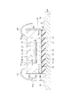
- FIG. 6 is a sectional view taken along the line VI-VI in FIG. 5;
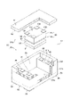
- FIG. 10 is an exploded perspective view showing a piezoelectric device of Embodiment 2;
- FIG. 10 is an exploded perspective view showing the inside of the first package in the piezoelectric device of Embodiment 2;
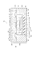
- FIG. 10 is a cross-sectional view showing a piezoelectric device of Embodiment 3;
- FIG. 11 is a cross-sectional view showing a piezoelectric device of Embodiment 4;
- FIG. 11 is a cross-sectional view showing a piezoelectric device of Embodiment 5;
- FIG. 11 is a cross-sectional view showing a piezoelectric device of Embodiment 6;
- FIG. 1 and 3 the mounting member 50 is cut away.
- FIG. 4 a part of the substrate 30a is cut away.
- the structure inside the package 30 (piezoelectric element 20, etc.) is shown only in FIGS.
- the piezoelectric device 11 includes a piezoelectric element 20, a package 30 containing at least the piezoelectric element 20, and a mounting member 50 on which the package 30 is mounted. and an absorbent body 60.
- the piezoelectric element 20 has a substantially rectangular shape in plan view, and includes a crystal piece 27 having a first main surface 21 and a second main surface 22 that are in a front-back relationship, and a crystal piece 27 having a first main surface 21 and a second main surface 22 . and electrodes 23 and 24 extending to the surface 22 .
- the crystal piece 27 is made of, for example, an AT cut plate.
- the electrodes 23 and 24 are insulated from each other, divided into an excitation electrode, an extraction electrode, a pad electrode, and the like, and extend from the first main surface 21 to the second main surface 22 across the side surfaces.
- the piezoelectric element 20 operates to output a signal with a constant oscillation frequency based on the piezoelectric effect and the inverse piezoelectric effect of the crystal piece 27 .
- the piezoelectric element 20 is a thickness-shear vibration element, but instead of this, a tuning-fork type bending vibration element, a contour-shear vibration element, or the like may be used.
- a piezoelectric element made of ceramics or the like may be used instead of the crystal oscillator.
- the planar shape of the piezoelectric element 20 is not limited to a rectangular shape, and may be any shape, such as a circular shape, an elliptical shape, or a polygonal shape.
- the package 30 includes a base 30a on which the piezoelectric element 20 is mounted, and a lid 30b that hermetically seals the piezoelectric element 20 by bonding to the base 30a.
- the package 30 in Embodiment 1 is a piezoelectric vibrator, it may be SPXO, VCXO, TCXO, or OCXO.
- the three-dimensional shape of the package 30 is not limited to a rectangular parallelepiped shape, and may be, for example, a columnar shape or an elliptical columnar shape.
- the base body 30 a includes a substrate portion 33 on which the piezoelectric element 20 is mounted and a frame portion 34 located on the periphery of the substrate portion 33 .
- the substrate portion 33 includes a first main surface 31 and a second main surface 32 which are in a front-back relationship, a pair of piezoelectric element pads 36 and 37 provided on the first main surface 31, and four corners of the second main surface 32. Each has an external terminal 38 provided.
- the frame portion 34 is provided in the shape of a square frame on the peripheral edge of the first main surface 31 of the substrate portion 33 .
- the inside of the package 30 is a recessed space 35 surrounded by the substrate portion 33 and the frame portion 34 .
- the electrodes 23 and 24 of the piezoelectric element 20 and the piezoelectric element pads 36 and 37 are electrically connected by bonding materials 25 and 26 such as a conductive adhesive.
- the substrate part 33 and the frame part 34 are made of laminated ceramic plates, for example, in which a plurality of green sheets are laminated and fired.
- the piezoelectric element pads 36 and 37 and the external terminals 38 are electrically connected to each other by internal wiring (not shown) formed in the substrate portion 33 and the frame portion 34 .
- the internal wiring consists of, for example, conductor patterns or via-hole conductors printed on a green sheet.
- the piezoelectric element pads 36 and 37 and the external terminals 38 are composed of, for example, a surface Au (gold) layer and an underlying Ni (nickel) layer.
- the lid body 30b is a rectangular flat plate, and has a first main surface 41 and a second main surface 42 that are in a front-back relationship.
- the material of the lid 30b is, for example, metal such as Kovar or ceramics.
- the lid 30b is joined to the base 30a by electric welding or glass sealing to hermetically seal the concave space 35.
- the lid 30b and the external terminal 38 are electrically connected by internal wiring (not shown) formed in the substrate portion 33 and the frame portion 34. As shown in FIG.
- the mounting member 50 is a component in electronic equipment on which the piezoelectric device 11 is mounted, and has a principal surface 51 and packaging pads 52 .
- An example of the mounting member 50 is a printed wiring board.
- a printed wiring board is a synthetic resin board on which lands and wiring patterns (not shown) are formed with copper foil or the like.
- the package pads 52 are provided on the main surface 51 at positions corresponding to the external terminals 38 of the package 30 .
- the package pads 52 and the external terminals 38 are electrically connected by wires 53 .
- the wire 53 is made of metal such as gold or aluminum and has flexibility. A common wire bonding technique is used for the connection method of the wire 53 .
- the package pad 52 is electrically connected to a predetermined location by a wiring pattern (not shown) formed on the main surface 51 of the mounting member 50, inside, or on the back surface.
- the mounting member 50 may be a laminated ceramic plate or the like.
- the vibration absorber 60 is a rectangular flat plate, and has a first main surface 61 and a second main surface 62 that are opposite to each other. Any material can be used for the vibration absorber 60 as long as it can absorb the vibration transmitted from the mounting member 50 to the package 30.
- a gel-like material particularly silicon gel (polymer gel composition) is preferable.
- Silicon-based gel is a moderately soft gel-like material whose main raw material is silicone, and is commercially available, for example, as ⁇ GEL (registered trademark).
- ⁇ GEL registered trademark
- the vibration absorber 60 is not limited to a rectangular shape, and may be any shape, such as a circular shape, an elliptical shape, or a polygonal shape.
- the number of vibration absorbers 60 is not limited to one, and may be plural.
- the bonding materials 25 and 26 made of a conductive adhesive are applied to the piezoelectric element pads 36 and 37 .
- the electrodes 23 and 24 of the piezoelectric element 20 are placed on the bonding materials 25 and 26, and the bonding materials 25 and 26 are cured by heat treatment at a predetermined temperature and time.
- the piezoelectric element 20 is fixed on the substrate portion 33 in a cantilever manner.
- the package 30 is completed by sealing the concave space 35 of the base 30a with the lid 30b.
- the package 30 is turned upside down (with the lid 30b side down) from the state shown in FIG. 4 (with the lid 30b side up). Then, the package 30 is fixed onto the main surface 51 of the mounting member 50 via the vibration absorber 60 .
- the external terminals 38 of the package 30 and the package pads 52 of the mounting member 50 are connected by wires 53 .
- the piezoelectric device 11 is mounted on the mounting member 50 .
- the vibration absorber 60 between the mounting member 50 and the package 30, the vibration of the mounting member 50 is absorbed by the vibration absorber 60, so that the vibration transmitted from the mounting member 50 to the package 30 is suppressed. be. Therefore, according to the piezoelectric device 11, further stabilization of the oscillation frequency can be achieved.
- FIG. 5 shows a state before the cover 80b is joined to the base 80a, with a part of the base 80a cut away.
- FIG. 7 a part of the lid 80b and a part of the base 80a are cut away.
- FIG. 8 a part of the base 130a is cut away.
- the structure (piezoelectric element 20, etc.) inside the first package 30 is shown only in FIGS.
- the piezoelectric device 12 includes a piezoelectric element 20, an electronic element 70 for driving the piezoelectric element 20, a first package 130 containing the piezoelectric element 20 and the electronic element 70, and a second package 80 further containing the first package 130. and a vibration absorber 60 that supports the first package 130 within the second package 80 and absorbs vibration transmitted from the second package 80 to the first package 130 .
- the following description will focus on the portions that differ from the first embodiment. Since the piezoelectric element 20 is the same as the piezoelectric element in the first embodiment, the description is omitted.
- the first package 130 includes a base 130a on which the electronic element 70 and the piezoelectric element 20 are mounted, and a lid 130b that hermetically seals the electronic element 70 and the piezoelectric element 20 by bonding to the base 130a.
- the first package 130 in the second embodiment is TCXO, but may be VCXO or OCXO.
- the three-dimensional shape of the first package 130 and the second package 80 is not limited to a rectangular parallelepiped shape, and may be, for example, a columnar shape or an elliptical columnar shape.
- the base 130a includes a substrate portion 133 on which the electronic element 70 is mounted, a first frame portion 134a positioned on the periphery of the substrate portion 133 and on which the piezoelectric element 20 is mounted, and a second frame portion positioned on the periphery of the first frame portion 134a. and a portion 134b.
- the substrate portion 133 includes a first main surface 131a and a second main surface 132 which are in front-back relationship, a plurality of electronic element pads 139 provided on the first main surface 131a, and four corners of the second main surface 132, respectively. It has an external terminal 138 .
- the first frame portion 134a has a main surface 131b and a pair of piezoelectric element pads 136 and 137 provided on the main surface 131b.
- the first frame portion 134a is provided in the shape of a square frame on the periphery of the first main surface 131a of the substrate portion 133
- the second frame portion 134b is provided in the shape of a square frame on the periphery of the main surface 131b of the first frame portion 134a. It is The inside of the first package 130 is a recessed space 135 surrounded by the substrate portion 133, the first frame portion 134a, and the second frame portion 134b.
- the electrodes 23 and 24 of the piezoelectric element 20 and the piezoelectric element pads 136 and 137 are electrically connected by bonding materials 25 and 26 such as a conductive adhesive.
- the substrate portion 133, the first frame portion 134a and the second frame portion 134b are made of laminated ceramic plates, for example, by laminating and firing a plurality of green sheets.
- the piezoelectric element pads 136 and 137, the external terminal 138, and the electronic element pad 139 are interconnected by internal wiring (not shown) formed in the substrate portion 133, the first frame portion 134a, and the second frame portion 134b. electrically connected.
- the internal wiring consists of, for example, conductor patterns or via-hole conductors printed on a green sheet.
- the piezoelectric element pads 136 and 137, the external terminals 138, and the electronic element pads 139 are composed of, for example, a surface Au layer and an underlying Ni layer.
- the lid body 130b is a rectangular flat plate, and has a first main surface 141 and a second main surface 142 that are in front-back relationship.
- the material of the lid 130b is, for example, metal such as Kovar or ceramics.
- the lid 130b is joined to the base 130a by electric welding or glass sealing to hermetically seal the concave space 135.
- the lid 130b and the external terminal 138 are electrically connected by internal wiring (not shown) formed in the substrate portion 133, the first frame portion 134a and the second frame portion 134b.
- the electronic element 70 is an IC having the function of the temperature sensor 71 and the function of the oscillation circuit of the piezoelectric element 20, etc., and is an FC (Flip Chip) in which the connection terminals 72 are bumps.
- the bumps are made of gold or solder, for example, and are electrically connected to the electronic element pads 139 .
- the connection terminals 72 and the electronic element pads 139 are provided in the same number. That is, the electronic element 70 is mounted on the base 130a via the connection terminals 72 with the circuit forming surface including the connection terminals 72 of the electronic element 70 facing the electronic element pads 139 of the first main surface 131a, that is, face down. .
- the temperature sensor 71 utilizes, for example, the forward voltage of a pn junction formed within the IC.
- the forward voltage of this pn junction decreases as the temperature increases. Therefore, voltage information can be obtained by applying a constant current to the pn junction and measuring the forward voltage. Temperature information of the electronic element 70 and thus the piezoelectric element 20 can be obtained by converting from the voltage information.
- the electronic element 70 may be a thermistor or a diode consisting only of a temperature sensor, or may be a resin molded product or a package, not limited to FC. Wires made of aluminum, gold, or the like may be used instead of the bumps for the connection terminals 72 .
- the second package 80 includes a base 80a on which the first package 130 is mounted, and a lid body 80b that hermetically seals the first package 130 by bonding to the base 80a.
- the base 80a includes a substrate portion 83 on which the first package 130 is mounted, a first frame portion 84a located on the periphery of the substrate portion 83, and a second frame portion 84b located on the periphery of the first frame portion 84a.
- the substrate portion 83 has a first principal surface 81 a and a second principal surface 82 that are in a front-back relationship, and external terminals 88 provided at the four corners of the second principal surface 82 .
- the first frame portion 84a has a main surface 81b and a package pad 86 provided on the main surface 81b.
- the first frame portion 84a is provided in the shape of a square frame on the periphery of the first main surface 81a of the substrate portion 83
- the second frame portion 84b is provided in the shape of a square frame on the periphery of the main surface 81b of the first frame portion 84a. It is The inside of the second package 80 is a recessed space 85 surrounded by the substrate portion 83, the first frame portion 84a, and the second frame portion 84b.
- the external terminals 138 of the first package 130 and the package pads 86 are electrically connected by wires 87 .
- the wire 87 is made of metal such as gold or aluminum and has flexibility. A common wire bonding technique is used for the connection method of the wire 87 .
- the substrate portion 83, the first frame portion 84a and the second frame portion 84b are made of laminated ceramic plates, for example, by laminating and firing a plurality of green sheets.
- the package pads 86 and the external terminals 88 are electrically connected to each other by internal wiring (not shown) formed in the substrate portion 83, the first frame portion 84a and the second frame portion 84b.
- the internal wiring consists of, for example, conductor patterns or via-hole conductors printed on a green sheet.
- the package pads 86 and the external terminals 88 are composed of, for example, a surface Au layer and an underlying Ni layer.
- the lid body 80b is a rectangular flat plate, and has a first main surface 91 and a second main surface 92 that are in a front-back relationship.
- the material of the lid 80b is, for example, metal such as Kovar or ceramics.
- the lid 80b is joined to the base 80a by electrical welding or glass sealing, and hermetically seals the concave space 85. As shown in FIG.
- the lid 80b and the external terminal 88 are electrically connected by internal wiring (not shown) formed in the substrate portion 83, the first frame portion 84a and the second frame portion 84b.
- the vibration absorber 60 is similar to the vibration absorber in Embodiment 1, but the first principal surface 61 is fixed to the first principal surface 81a of the second package 80 via an adhesive, and the second principal surface 62 is It is fixed to the first package 130 via an adhesive.
- connection terminals 72 of the electronic element 70 faces the first main surface 131a in the recessed space 135, and the positions of the electronic element pads 139 and the connection terminals 72 are aligned. Heat or ultrasonic waves are applied while pressing the connection terminal 72 against the pad 139 . As a result, the connection terminals 72 are joined to the electronic element pads 139 , and the electronic element 70 is mounted in the first package 130 .
- the bonding materials 25 and 26 made of a conductive adhesive are applied to the piezoelectric element pads 136 and 137.
- the electrodes 23 and 24 of the piezoelectric element 20 are placed on the bonding materials 25 and 26, and the bonding materials 25 and 26 are cured by heat treatment at a predetermined temperature and time.
- the piezoelectric element 20 is fixed on the first frame portion 134 a in a cantilever beam shape, and the piezoelectric element 20 is mounted inside the first package 130 .
- the first package 130 is completed by sealing the concave space 135 of the base 130a with the lid 130b.
- the first package 130 is turned upside down (with the lid 130b side down) from the state shown in FIG. 8 (with the lid 130b side up). Then, the first package 130 is fixed on the first major surface 81a inside the second package 80 via the vibration absorber 60 .
- the external terminals 138 of the first package 130 and the package pads 86 of the second package 80 are connected by wires 87 .
- the first package 130 is mounted inside the second package 80 .
- the piezoelectric device 12 configured as described above is fixed to the printed wiring board by soldering, Au bumps, conductive adhesive, or the like at the bottom surface of the external terminals 88, thereby forming an electronic device on the surface of the printed wiring board.
- the piezoelectric device 12 is used as an oscillation source in various electronic devices such as personal computers, clocks, game machines, communication devices, and in-vehicle devices such as car navigation systems.
- the piezoelectric device 12 has a structure in which the piezoelectric element 20 and the electronic element 70 are housed in the first package 130 , and the first package 130 is further housed in the second package 80 . Therefore, according to the piezoelectric device 12, the first package 130 housing the piezoelectric element 20 and the electronic element 70 is isolated from the surrounding atmosphere by the second package 80, so that temperature changes in the surrounding atmosphere are Since it becomes difficult for the light to reach the electronic element 70, the oscillation frequency can be stabilized.
- the vibration absorber 60 between the second package 80 and the first package 130, the vibration of the second package 80 is absorbed by the vibration absorber 60. Vibration transmitted to the one package 130 is suppressed. Therefore, according to the piezoelectric device 12, these effects can be combined to achieve further stabilization of the oscillation frequency. In particular, the piezoelectric device 12 exhibits a remarkable effect against sudden temperature changes and vibrations caused by the wind of the cooling fan. Other configurations, actions and effects of the second embodiment are the same as those of the first embodiment.
- the piezoelectric device 13 of Embodiment 3 will be described.
- the cross section shown in FIG. 9 corresponds to the cross sections shown in FIGS.
- the piezoelectric device 13 of the third embodiment has many parts in common with the piezoelectric device 11 (FIG. 2) of the first embodiment and the piezoelectric device 12 (FIG. 6) of the second embodiment. Therefore, the first package 30 uses the reference numerals of the package 30 (FIG. 2) in the first embodiment, and the second package 80 uses the reference numerals of the second package 80 (FIG. 6) in the second embodiment.
- the piezoelectric device 13 includes a piezoelectric element 20, a first package 30 containing the piezoelectric element 20, an electronic element 70 for driving the piezoelectric element 20, and a second package 80 further containing the electronic element 70 and the first package 30. , and a vibration absorber 60 that supports the first package 30 within the second package 80 and absorbs vibration transmitted from the second package 80 to the first package 30 .
- the first package 30 has a first substrate 30a on which the piezoelectric element 20 is mounted, and a first lid 30b that hermetically seals the piezoelectric element 20 together with the first substrate 30a.
- the second package 80 includes a second base 80a on which the electronic element 70 is mounted and the first package 30 is mounted via the vibration absorber 60, and the electronic element 70 and the first package 30 are hermetically sealed together with the second base 80a. and a second lid body 80b.
- the piezoelectric device 13 differs from the piezoelectric device 12 of Embodiment 2 (FIG. 6) in that the electronic element 70 is mounted on the first main surface 81a of the second package 80 instead of inside the first package 30.
- the electronic device pads 89 are formed on the first main surface 81a, and the electronic device 70 and the first package 30 are arranged side by side on the first main surface 81a.
- the piezoelectric device 13 since the electronic element 70 and the first package 30 are arranged side by side on the first main surface 81a, the heat conduction via the first main surface 81a is reduced between the electronic element 70 and the first package. The same conditions apply to 30. Therefore, the temperature sensor 71 in the electronic element 70 can more accurately measure the temperature of the piezoelectric element 20 in the first package 30, thereby improving the temperature compensation accuracy.
- Other configurations, actions and effects of the third embodiment are the same as those of the first and second embodiments. Therefore, according to the piezoelectric device 12, these effects can be combined to further stabilize the oscillation frequency.
- a piezoelectric device 14 according to Embodiment 4 will be described with reference to FIG. Also in the fourth embodiment, as in the third embodiment, the first package 30 uses the reference numerals of the package 30 (FIG. 2) in the first embodiment, and the second package 80 uses the second package 80 (FIG. 6) in the second embodiment. ) will be used.
- the piezoelectric device 14 includes a piezoelectric element 20, a first package 30 containing the piezoelectric element 20, an electronic element 70 for driving the piezoelectric element 20, and a second package 80 further containing the electronic element 70 and the first package 30. , and a vibration absorber 160 that supports the first package 30 within the second package 80 and absorbs vibration transmitted from the second package 80 to the first package 30 .
- the first package 30 has a first substrate 30a on which the piezoelectric element 20 is mounted, and a first lid 30b that hermetically seals the piezoelectric element 20 together with the first substrate 30a.
- the second package 80 includes a second base 80a on which the electronic element 70 is mounted and the first package 30 is mounted via a vibration absorber 160, and the electronic element 70 and the first package 30 are hermetically sealed together with the second base 80a. and a second lid body 80b.
- the piezoelectric device 14 differs from the piezoelectric device 12 (FIG. 9) of Embodiment 3 in that the electronic element 70 and the first package 30 overlap when viewed from above.
- the vibration absorber 160 is divided into two along two opposing sides of the first package 30 in plan view, and the first main surface 161 is attached to the first main surface 81a of the second package 80 via an adhesive.
- the second major surface 162 is fixed to the first package 30 via an adhesive.
- the electronic element 70 can be inserted between the pair of vibration absorbers 160 by setting the height of the vibration absorber 160 higher than the height of the electronic element 70 mounted on the first main surface 81a.
- the material and the like of the vibration absorber 60 are the same as those of the vibration absorber in the first embodiment.
- the vibration absorbers 160 may be provided at the four corners of the first package 30 in plan view.
- the piezoelectric device 14 since the electronic element 70 and the first package 30 overlap in plan view, the area occupied by the piezoelectric device 14 can be reduced, which contributes to miniaturization of electronic equipment incorporating the piezoelectric device 14. can.
- Other configurations, actions and effects of the third embodiment are the same as those of the first to third embodiments.
- a piezoelectric device 15 according to Embodiment 5 will be described with reference to FIG. Also in the fifth embodiment, as in the third embodiment, the first package 30 uses the reference numerals of the package 30 (FIG. 2) in the first embodiment, and the second package 80 uses the second package 80 (FIG. 6) in the second embodiment. ) will be used.
- the piezoelectric device 15 includes a piezoelectric element 20, a first package 30 containing the piezoelectric element 20, an electronic element 70 for driving the piezoelectric element 20, and a second package 80 further containing the electronic element 70 and the first package 30. , and a vibration absorber 60 that supports the first package 30 within the second package 80 and absorbs vibration transmitted from the second package 80 to the first package 30 .
- the first package 30 includes a first main surface 31 and a second main surface 32 that are in front-back relationship, and has the piezoelectric element 20 mounted on the first main surface 31 and the electronic element 70 mounted on the second main surface 32 . It has a substrate 30a and a first lid 30b that hermetically seals the piezoelectric element 20 together with the first substrate 30a.
- the second package 80 includes a second base 80a on which the first package 30 is mounted via the vibration absorber 60, and a second cover 80b that hermetically seals the electronic element 70 and the first package 30 together with the second base 80a. , have The connection terminals 72 of the electronic element 70 are electrically connected to the electronic element pads 39 provided on the second main surface 32 of the first substrate 30a.
- the piezoelectric device 15 differs from the piezoelectric device 14 (FIG. 10) of the fourth embodiment in that the piezoelectric element 20 is mounted on the first main surface 31 and the electronic element 70 is mounted on the second main surface 32 of the first package 30. different.
- the vibration absorber 60 is similar to the vibration absorber in Embodiment 1, but the first principal surface 61 is fixed to the first principal surface 81a of the second package 80 via an adhesive, and the second principal surface 62 is It is fixed to the first package 30 via an adhesive.
- the electronic element 70 is mounted on the first package 30 supported by the vibration absorber 60, not only the vibration transmitted from the second package 80 to the first package 30 but also the Vibration transmitted to the electronic element 70 is also suppressed by the vibration absorber 60 . Therefore, according to the piezoelectric device 15, malfunction of the electronic element 70 can be suppressed and the life of the electronic element 70 can be extended, and these effects can be combined to achieve further stabilization of the oscillation frequency.
- Other configurations, actions and effects of the third embodiment are the same as those of the first to fourth embodiments.
- a piezoelectric device 16 according to the sixth embodiment will be described with reference to FIG. Also in the sixth embodiment, as in the third embodiment, the first package 30 uses the reference numerals of the package 30 (FIG. 2) in the first embodiment, and the second package 80 uses the second package 80 (FIG. 6) in the second embodiment. ) will be used.
- the piezoelectric device 16 includes a piezoelectric element 20, a first package 30 containing the piezoelectric element 20, an electronic element 70 for driving the piezoelectric element 20, and a second package 80 further containing the electronic element 70 and the first package 30. , and a vibration absorber 260 that supports the first package 30 within the second package 80 and absorbs vibration transmitted from the second package 80 to the first package 30 .
- the first package 30 has a first substrate 30a on which the piezoelectric element 20 is mounted, and a first lid 30b that hermetically seals the piezoelectric element 20 together with the first substrate 30a.
- the second package 80 includes a second base 80a on which the electronic element 70 is mounted while the first package 30 is fixed via the vibration absorber 260, and an airtight seal between the electronic element 70 and the first package 30 together with the second base 80a. and a second lid body 80b that stops.
- the vibration absorber 260 has a first main surface 261 fixed to the electronic element 70 with an adhesive, and a second main surface 262 fixed to the first package 30 with an adhesive.
- the material and the like of the vibration absorber 260 are the same as those of the vibration absorber in the first embodiment.
- the piezoelectric device 16 has the vibration absorber 260 between the first package 30 and the electronic element 70 instead of the vibration absorber 260 between the first package 30 and the first main surface 81a. It differs from the piezoelectric device 14 (FIG. 9) of the third embodiment. According to the piezoelectric device 16, by inserting the electronic element 70 and the vibration absorber 60 between the second package 80 and the first package 130, the vibration of the second package 80 is damped by the electronic element 70, and then the vibration is absorbed. Since the vibration is absorbed by the body 260, the vibration transmitted from the second package 80 to the first package 130 is further suppressed. Therefore, according to the piezoelectric device 16, further stabilization of the oscillation frequency can be achieved more reliably. Other configurations, actions and effects of the sixth embodiment are the same as those of the first to fourth embodiments.
- the present disclosure can be used as a piezoelectric device.
Landscapes
- Physics & Mathematics (AREA)
- Acoustics & Sound (AREA)
- Piezo-Electric Or Mechanical Vibrators, Or Delay Or Filter Circuits (AREA)
Abstract
圧電デバイス11は、圧電素子20と、少なくとも圧電素子20を内蔵したパッケージ30と、パッケージ30を実装する実装部材50においてパッケージ30を支持するとともに、実装部材50からパッケージ30へ伝わる振動を吸収する振動吸収体60と、を備えたものである。圧電素子20は、平面視して略四角形状であり、表裏関係にある第一主面21及び第二主面22を有する水晶片27と、水晶片27の第一主面21から第二主面22まで延びる電極23,24と、を備えた水晶振動素子である。
Description
本開示は、圧電素子を備えた圧電デバイスに関する。
圧電素子をパッケージ内に収めた圧電デバイスが広く普及している。また、圧電素子と電子素子とを備えた圧電デバイスも普及している。これらの圧電デバイスとしては、例えば、SPXO(Simple Packaged Crystal Oscillator:パッケージ水晶発振器)、VCXO(Voltage Controlled Crystal Oscillator:電圧制御水晶発振器)、TCXO(Tempe rature Compensated Crystal Oscillator:温度補償水晶発振器)、及び、OCXO(Oven Controlled Crystal Oscillator:恒温槽付水晶発振器)などが挙げられる。
更に、二つのパッケージによって圧電素子を二重に封止した圧電デバイスも知られている。例えば特許文献1には、圧電素子と電子素子とを第一パッケージ内に収め、その第一パッケージを更に第二パッケージ内に収めた圧電デバイスが開示されている。特許文献2には、圧電素子を第一パッケージ内に収め、その第一パッケージと電子素子とを更に第二パッケージ内に収めた圧電デバイスが開示されている。この種の圧電デバイスによれば、圧電素子を収納した第一パッケージが第二パッケージによって周囲の雰囲気から遮断されることにより、周囲の雰囲気の温度変化が圧電素子まで到達しにくくなるので、発振周波数の安定化が図れる。
本開示に係る圧電デバイスは、
圧電素子と、
少なくとも前記圧電素子を内蔵したパッケージと、
前記パッケージを実装する実装部材において前記パッケージを支持するとともに、前記実装部材から前記パッケージへ伝わる振動を吸収する振動吸収体と、
を備えたものである。
圧電素子と、
少なくとも前記圧電素子を内蔵したパッケージと、
前記パッケージを実装する実装部材において前記パッケージを支持するとともに、前記実装部材から前記パッケージへ伝わる振動を吸収する振動吸収体と、
を備えたものである。
以下、添付図面を参照しながら、本開示を実施するための形態(以下「実施形態」という。)について説明する。なお、本明細書及び図面において、実質的に同一の構成要素については同一の符号を用いることにより、重複説明を省略する。図面に描かれた形状は、見やすさ書きやすさを優先しているため、実際の寸法及び比率とは必ずしも一致していない。
<実施形態1>
図1乃至図4に基づき、実施形態1の圧電デバイス11について説明する。なお、図1及び図3では、実装部材50を切り欠いて示している。図4では、基体30aの一部を切り欠いて示している。パッケージ30内の構造(圧電素子20等)は、図2及び図4のみに示す。
図1乃至図4に基づき、実施形態1の圧電デバイス11について説明する。なお、図1及び図3では、実装部材50を切り欠いて示している。図4では、基体30aの一部を切り欠いて示している。パッケージ30内の構造(圧電素子20等)は、図2及び図4のみに示す。
圧電デバイス11は、圧電素子20と、少なくとも圧電素子20を内蔵したパッケージ30と、パッケージ30を実装する実装部材50においてパッケージ30を支持するとともに、実装部材50からパッケージ30へ伝わる振動を吸収する振動吸収体60と、を備えたものである。
圧電素子20は、平面視して略四角形状であり、表裏関係にある第一主面21及び第二主面22を有する水晶片27と、水晶片27の第一主面21から第二主面22まで延びる電極23,24と、を備えた水晶振動素子である。水晶片27は例えばATカット板からなる。電極23,24は、互いに絶縁されており、それぞれ励振電極、引き出し電極、パッド電極などに分けられ、第一主面21から側面を跨いで第二主面22まで延びている。
ここで、電極23,24を介して、水晶片27に交番電圧を印加する。すると、水晶片27は、第一主面21と第二主面22とが互いにずれるように厚みすべり振動を起こし、特定の発振周波数を発生させる。このように、圧電素子20は、水晶片27の圧電効果及び逆圧電効果に基づき、一定の発振周波数の信号を出力するように動作する。
圧電素子20は厚みすべり振動素子であるが、これに代えて音叉型屈曲振動素子又は輪郭すべり振動素子などを用いてもよい。なお、水晶振動素子の代わりに、セラミックスなどからなる圧電素子を用いてもよい。圧電素子20の平面形状は、四角形状に限らずどのような形状でもよく、例えば、円形状、楕円形状、又は多角形状などとしてもよい。
パッケージ30は、圧電素子20を実装する基体30aと、基体30aに接合することにより圧電素子20を気密封止する蓋体30bと、を備えている。本実施形態1におけるパッケージ30は、圧電振動子であるが、SPXO、VCXO、TCXO又はOCXOとしてもよい。パッケージ30の立体形状は、直方体状に限らず、例えば円柱状又は楕円柱状などとしてもよい。
基体30aは、圧電素子20を実装する基板部33と、基板部33の周縁に位置する枠部34と、を含む。基板部33は、表裏関係にある第一主面31及び第二主面32、第一主面31に設けられた一対の圧電素子用パッド36,37、並びに、第二主面32の四隅にそれぞれ設けられた外部端子38を有する。枠部34は、基板部33の第一主面31の周縁上に、四角枠状に設けられている。パッケージ30内は、基板部33と枠部34とによって囲まれた凹部空間35になっている。圧電素子20の電極23,24と圧電素子用パッド36,37とは、導電性接着剤などの接合材25,26によって電気的に接続される。
基板部33及び枠部34は、例えば複数枚のグリーンシートが積層及び焼成された積層セラミックス板からなる。圧電素子用パッド36,37と外部端子38とは、基板部33及び枠部34に形成された内部配線(図示せず)によって、相互に電気的に接続されている。その内部配線は、例えばグリーンシートに印刷された導体パターン又はビアホール導体からなる。圧電素子用パッド36,37及び外部端子38は、例えば表面のAu(金)層と、その下地のNi(ニッケル)層とからなる。
蓋体30bは、四角状の平板となっており、表裏関係にある第一主面41及び第二主面42を有する。蓋体30bの材質は、例えばコバール(Kovar)などの金属又はセラミックスなどである。また、蓋体30bは、基体30aに電気溶接又はガラス封止などにより接合され、凹部空間35を気密封止する。蓋体30bと外部端子38とは、基板部33及び枠部34に形成された内部配線(図示せず)によって電気的に接続されている。
実装部材50は、圧電デバイス11が実装される電子機器内の部品であり、主面51及びパッケージ用パッド52を有する。実装部材50の一例として、プリント配線板が挙げられる。プリント配線板は、合成樹脂板上に銅箔などでランド及び配線パターン(図示せず)が形成されたものである。パッケージ用パッド52は、主面51においてパッケージ30の外部端子38に対応する位置に設けられる。パッケージ用パッド52と外部端子38とは、ワイヤ53によって電気的に接続される。ワイヤ53は、例えば金又はアルミニウムなどの金属からなり、可撓性を有する。ワイヤ53の接続方法は、一般的なワイヤボンディング技術を用いる。なお、パッケージ用パッド52は、実装部材50の主面51、内部又は裏面に形成された配線パターン(図示せず)によって、所定箇所に電気的に接続されている。また、実装部材50は、積層セラミックス板などを用いてもよい。
振動吸収体60は、四角形状の平板となっており、表裏関係にある第一主面61及び第二主面62を有する。振動吸収体60の材質は、実装部材50からパッケージ30へ伝わる振動を吸収できればどのようなものでも良いが、一例としてゲル状材料、特にシリコン系ゲル(高分子ゲル組成物)が好適である。シリコン系ゲルは、シリコーンを主原料とする適度に柔らかいゲル状素材であり、例えばαGEL(登録商標)として市販されている。振動吸収体60がシリコン系ゲルである場合、シリコン系ゲルを四角形状の平板に加工し、第二主面62を接着剤を介してパッケージ30に固定し、第一主面61を接着剤を介して実装部材50に固定する。その接着剤としては、アクリル粘着剤が適当である。なお、振動吸収体60の平面形状は、四角形状に限らずどのような形状でもよく、例えば、円形状、楕円形状、又は多角形状などとしてもよい。振動吸収体60の個数についても、一つに限らず、複数としてもよい。
次に、圧電デバイス11の組み立て方法について説明する。
まず、図4に示すように、基板部33の第一主面31において、圧電素子用パッド36,37に、導電性接着剤からなる接合材25,26を塗布する。そして、接合材25,26に圧電素子20の電極23,24を載置し、所定の温度及び時間の熱処理を施すことにより、接合材25,26を硬化させる。これにより、圧電素子20は基板部33上に片持ち梁状に固定される。そして、基体30aの凹部空間35を蓋体30bによって封止すると、パッケージ30が完成する。
続いて、図3に示すように、パッケージ30を図4に示す状態(蓋体30b側が上)から逆さ(蓋体30b側が下)にする。そして、パッケージ30を、振動吸収体60を介して実装部材50の主面51上に固定する。
最後に、図1に示すように、パッケージ30の外部端子38と実装部材50のパッケージ用パッド52とを、ワイヤ53によって接続する。これにより、圧電デバイス11が実装部材50上に実装される。
次に、圧電デバイス11の作用及び効果について説明する。本発明者は、圧電デバイスの発振周波数の更なる安定化を求めて、実験及び考察を繰り返した。その結果、実装部材(例えばプリント配線板)からの微細な振動(例えば冷却ファンの風や冷却ファンの振動)が、圧電デバイスの発振周波数に影響を与えていることを突き止めた。この影響は、圧電素子の持つ圧電気直接効果(加圧による電圧発生)に起因すると考えられる。本開示は、この知見に基づきなされたものである。すなわち、実装部材50とパッケージ30との間に振動吸収体60を挿入することにより、実装部材50の振動が振動吸収体60で吸収されるので、実装部材50からパッケージ30に伝わる振動が抑制される。よって、圧電デバイス11によれば、発振周波数の更なる安定化を達成できる。
<実施形態2>
図5乃至図8に基づき、実施形態2の圧電デバイス12について説明する。なお、図5では、蓋体80bを基体80aに接合する前の状態を、基体80aの一部を切り欠いて示している。図7では、蓋体80bの一部及び基体80aの一部をそれぞれ切り欠いて示している。図8では、基体130aの一部を切り欠いて示している。第一パッケージ30内の構造(圧電素子20等)は、図6及び図8のみに示す。
図5乃至図8に基づき、実施形態2の圧電デバイス12について説明する。なお、図5では、蓋体80bを基体80aに接合する前の状態を、基体80aの一部を切り欠いて示している。図7では、蓋体80bの一部及び基体80aの一部をそれぞれ切り欠いて示している。図8では、基体130aの一部を切り欠いて示している。第一パッケージ30内の構造(圧電素子20等)は、図6及び図8のみに示す。
圧電デバイス12は、圧電素子20と、圧電素子20を駆動する電子素子70と、圧電素子20及び電子素子70を内蔵した第一パッケージ130と、第一パッケージ130を更に内蔵した第二パッケージ80と、第二パッケージ80内で第一パッケージ130を支持するとともに、第二パッケージ80から第一パッケージ130へ伝わる振動を吸収する振動吸収体60と、を備えたものである。以下、実施形態1と異なる部分を中心に説明する。圧電素子20については、実施形態1における圧電素子と同様であるので、説明を省略する。
第一パッケージ130は、電子素子70及び圧電素子20を実装する基体130aと、基体130aに接合することにより電子素子70及び圧電素子20を気密封止する蓋体130bと、を備えている。本実施形態2における第一パッケージ130は、TCXOであるが、VCXO又はOCXOなどとしてもよい。第一パッケージ130及び第二パッケージ80の立体形状は、直方体状に限らず、例えば円柱状又は楕円柱状などとしてもよい。
基体130aは、電子素子70を実装する基板部133と、基板部133の周縁に位置するとともに圧電素子20を実装する第一枠部134aと、第一枠部134aの周縁に位置する第二枠部134bとを含む。基板部133は、表裏関係にある第一主面131a及び第二主面132、第一主面131aに複数設けられた電子素子用パッド139、並びに、第二主面132の四隅にそれぞれ設けられた外部端子138を有する。第一枠部134aは、主面131b及び主面131bに設けられた一対の圧電素子用パッド136,137を有する。第一枠部134aは基板部133の第一主面131aの周縁上に四角枠状に設けられ、第二枠部134bは第一枠部134aの主面131bの周縁上に四角枠状に設けられている。第一パッケージ130内は、基板部133と第一枠部134aと第二枠部134bとによって囲まれた凹部空間135になっている。圧電素子20の電極23,24と圧電素子用パッド136,137とは、導電性接着剤などの接合材25,26によって電気的に接続される。
基板部133、第一枠部134a及び第二枠部134bは、例えば複数枚のグリーンシートが積層及び焼成された積層セラミックス板からなる。圧電素子用パッド136,137と外部端子138と電子素子用パッド139とは、基板部133、第一枠部134a及び第二枠部134bに形成された内部配線(図示せず)によって、相互に電気的に接続されている。その内部配線は、例えばグリーンシートに印刷された導体パターン又はビアホール導体からなる。圧電素子用パッド136,137、外部端子138及び電子素子用パッド139は、例えば表面のAu層と、その下地のNi層とからなる。
蓋体130bは、四角状の平板となっており、表裏関係にある第一主面141及び第二主面142を有する。蓋体130bの材質は、例えばコバールなどの金属又はセラミックスなどである。また、蓋体130bは、基体130aに電気溶接又はガラス封止などにより接合され、凹部空間135を気密封止する。蓋体130bと外部端子138とは、基板部133、第一枠部134a及び第二枠部134bに形成された内部配線(図示せず)によって電気的に接続されている。
電子素子70は、温度センサ71の機能及び圧電素子20の発振回路等の機能を有するICであるとともに、接続端子72がバンプになっているFC(Flip Chip:フリップチップ)である。そのバンプは、例えば金又ははんだからなり、電子素子用パッド139に電気的に接続される。接続端子72と電子素子用パッド139とは、同じ数だけ設けられている。つまり、電子素子70の接続端子72を含む回路形成面を第一主面131aの電子素子用パッド139に向けて、すなわちフェイスダウンで、電子素子70を接続端子72を介して基体130aに実装する。温度センサ71は、例えばIC内に形成されたpn接合の順方向電圧を利用するものである。このpn接合の順方向電圧は、温度が高くなるほど小さくなる。そのため、pn接合に一定電流を流しておいて順方向電圧を測定することによって、電圧情報を得ることができる。その電圧情報から換算することで電子素子70ひいては圧電素子20の温度情報を得ることができる。なお、電子素子70は、温度センサのみからなる例えばサーミスタ又はダイオードなどとしてもよいし、FCに限らず樹脂モールド品又はパッケージ入りでもよい。接続端子72の部分は、バンプに代えて、アルミニウム又は金などからなるワイヤを用いてもよい。
第二パッケージ80は、第一パッケージ130を実装する基体80aと、基体80aに接合することにより第一パッケージ130を気密封止する蓋体80bと、を備えている。
基体80aは、第一パッケージ130を実装する基板部83と、基板部83の周縁に位置する第一枠部84aと、第一枠部84aの周縁に位置する第二枠部84bとを含む。基板部83は、表裏関係にある第一主面81a及び第二主面82、並びに、第二主面82の四隅にそれぞれ設けられた外部端子88を有する。第一枠部84aは、主面81b及び主面81bに設けられたパッケージ用パッド86を有する。第一枠部84aは基板部83の第一主面81aの周縁上に四角枠状に設けられ、第二枠部84bは第一枠部84aの主面81bの周縁上に四角枠状に設けられている。第二パッケージ80内は、基板部83と第一枠部84aと第二枠部84bとによって囲まれた凹部空間85になっている。第一パッケージ130の外部端子138とパッケージ用パッド86とは、ワイヤ87よって電気的に接続される。ワイヤ87は、例えば金又はアルミニウムなどの金属からなり、可撓性を有する。ワイヤ87の接続方法は、一般的なワイヤボンディング技術を用いる。
基板部83、第一枠部84a及び第二枠部84bは、例えば複数枚のグリーンシートが積層及び焼成された積層セラミックス板からなる。パッケージ用パッド86と外部端子88とは、基板部83、第一枠部84a及び第二枠部84bに形成された内部配線(図示せず)によって、相互に電気的に接続されている。その内部配線は、例えばグリーンシートに印刷された導体パターン又はビアホール導体からなる。パッケージ用パッド86及び外部端子88は、例えば表面のAu層と、その下地のNi層とからなる。
蓋体80bは、四角状の平板となっており、表裏関係にある第一主面91及び第二主面92を有する。蓋体80bの材質は、例えばコバールなどの金属又はセラミックスなどである。また、蓋体80bは、基体80aに電気溶接又はガラス封止などにより接合され、凹部空間85を気密封止する。蓋体80bと外部端子88とは、基板部83、第一枠部84a及び第二枠部84bに形成された内部配線(図示せず)によって電気的に接続されている。
振動吸収体60は、実施形態1における振動吸収体と同様であるが、第一主面61が接着剤を介して第二パッケージ80の第一主面81aに固定され、第二主面62が接着剤を介して第一パッケージ130に固定されている。
次に、圧電デバイス12の組み立て方法について説明する。
まず、図8に示すように、凹部空間135内の第一主面131aに電子素子70の接続端子72の形成面を向け、電子素子用パッド139と接続端子72との位置を合わせ、電子素子用パッド139に接続端子72を押し付けるとともに熱又は超音波を加える。これにより、電子素子用パッド139に接続端子72が接合され、第一パッケージ130内に電子素子70が実装される。
続いて、第一枠部134aの主面131bにおいて、圧電素子用パッド136,137に、導電性接着剤からなる接合材25,26を塗布する。そして、接合材25,26に圧電素子20の電極23,24を載置し、所定の温度及び時間の熱処理を施すことにより、接合材25,26を硬化させる。これにより、圧電素子20は第一枠部134a上に片持ち梁状に固定され、第一パッケージ130内に圧電素子20が実装される。
続いて、基体130aの凹部空間135を蓋体130bによって封止すると、第一パッケージ130が完成する。
続いて、図7に示すように、第一パッケージ130を図8に示す状態(蓋体130b側が上)から逆さ(蓋体130b側が下)にする。そして、第一パッケージ130を、振動吸収体60を介して第二パッケージ80内の第一主面81a上に固定する。
続いて、図5に示すように、第一パッケージ130の外部端子138と第二パッケージ80のパッケージ用パッド86とを、ワイヤ87によって接続する。これにより、第二パッケージ80内に第一パッケージ130が実装される。
最後に、第二パッケージ80の凹部空間85を蓋体80bによって封止すると、圧電デバイス12が完成する。
以上のように構成された圧電デバイス12は、はんだ付け、Auバンプ又は導電性接着剤などによってプリント配線板に外部端子88の底面が固定されることによって、電子機器を構成するプリント配線板の表面に実装される。そして、圧電デバイス12は、例えば、パーソナルコンピュータ、時計、ゲーム機、通信機、又は、カーナビゲーションシステム等の車載機器などの種々の電子機器で発振源として用いられる。
次に、圧電デバイス12の作用及び効果について説明する。
圧電デバイス12は、圧電素子20と電子素子70とを第一パッケージ130内に収め、第一パッケージ130を更に第二パッケージ80内に収めた構造である。そのため、圧電デバイス12によれば、圧電素子20及び電子素子70を収納した第一パッケージ130が第二パッケージ80によって周囲の雰囲気から遮断されることにより、周囲の雰囲気の温度変化が圧電素子20及び電子素子70まで到達しにくくなるので、発振周波数の安定化が図れる。
これに加え、第二パッケージ80と第一パッケージ130との間に振動吸収体60を挿入することにより、第二パッケージ80の振動が振動吸収体60で吸収されるので、第二パッケージ80から第一パッケージ130に伝わる振動が抑制される。よって、圧電デバイス12によれば、これらの効果が相俟って発振周波数の更なる安定化を達成できる。特に、冷却ファンの風による急激な温度変化及び振動に対して、圧電デバイス12は顕著な効果を奏する。本実施形態2のその他の構成、作用及び効果は、実施形態1のそれらと同様である。
<実施形態3>
図9に基づき、実施形態3の圧電デバイス13について説明する。図9に示す断面は、図2及び図6に示す断面に対応する。これらの対応関係からわかるように、本実施形態3の圧電デバイス13は、実施形態1の圧電デバイス11(図2)及び実施形態2の圧電デバイス12(図6)と共通する部分が多い。そのため、第一パッケージ30は実施形態1におけるパッケージ30(図2)の符号を用い、第二パッケージ80は実施形態2における第二パッケージ80(図6)の符号を用いることにする。
図9に基づき、実施形態3の圧電デバイス13について説明する。図9に示す断面は、図2及び図6に示す断面に対応する。これらの対応関係からわかるように、本実施形態3の圧電デバイス13は、実施形態1の圧電デバイス11(図2)及び実施形態2の圧電デバイス12(図6)と共通する部分が多い。そのため、第一パッケージ30は実施形態1におけるパッケージ30(図2)の符号を用い、第二パッケージ80は実施形態2における第二パッケージ80(図6)の符号を用いることにする。
圧電デバイス13は、圧電素子20と、圧電素子20を内蔵した第一パッケージ30と、圧電素子20を駆動する電子素子70と、電子素子70及び第一パッケージ30を更に内蔵した第二パッケージ80と、第二パッケージ80内で第一パッケージ30を支持するとともに、第二パッケージ80から第一パッケージ30へ伝わる振動を吸収する振動吸収体60と、を備えたものである。
第一パッケージ30は、圧電素子20を実装する第一基体30aと、圧電素子20を第一基体30aとともに気密封止する第一蓋体30bと、を有する。第二パッケージ80は、電子素子70を実装するとともに第一パッケージ30を振動吸収体60を介して実装する第二基体80aと、電子素子70及び第一パッケージ30を第二基体80aとともに気密封止する第二蓋体80bと、を有する。
圧電デバイス13は、電子素子70が第一パッケージ30内ではなく第二パッケージ80の第一主面81aに実装されている点で、実施形態2の圧電デバイス12(図6)と異なる。本実施形態3では、第一主面81aに電子素子用パッド89が形成されており、第一主面81a上に電子素子70と第一パッケージ30とが並んで配置されている。
圧電デバイス13によれば、第一主面81aに電子素子70と第一パッケージ30とが並んで配置されていることにより、第一主面81aを経由する熱伝導が電子素子70と第一パッケージ30とで同じ条件になる。そのため、電子素子70内の温度センサ71が第一パッケージ30内の圧電素子20の温度をより正確に測定できるので、温度補償精度を向上できる。本実施形態3のその他の構成、作用及び効果は、実施形態1、2のそれらと同様である。よって、圧電デバイス12によれば、これらの効果が相俟って発振周波数の更なる安定化をより一層達成できる。
<実施形態4>
図10に基づき、実施形態4の圧電デバイス14について説明する。本実施形態4においても、実施形態3と同様に、第一パッケージ30は実施形態1におけるパッケージ30(図2)の符号を用い、第二パッケージ80は実施形態2における第二パッケージ80(図6)の符号を用いることにする。
図10に基づき、実施形態4の圧電デバイス14について説明する。本実施形態4においても、実施形態3と同様に、第一パッケージ30は実施形態1におけるパッケージ30(図2)の符号を用い、第二パッケージ80は実施形態2における第二パッケージ80(図6)の符号を用いることにする。
圧電デバイス14は、圧電素子20と、圧電素子20を内蔵した第一パッケージ30と、圧電素子20を駆動する電子素子70と、電子素子70及び第一パッケージ30を更に内蔵した第二パッケージ80と、第二パッケージ80内で第一パッケージ30を支持するとともに、第二パッケージ80から第一パッケージ30へ伝わる振動を吸収する振動吸収体160と、を備えたものである。
第一パッケージ30は、圧電素子20を実装する第一基体30aと、圧電素子20を第一基体30aとともに気密封止する第一蓋体30bと、を有する。第二パッケージ80は、電子素子70を実装するとともに第一パッケージ30を振動吸収体160を介して実装する第二基体80aと、電子素子70及び第一パッケージ30を第二基体80aとともに気密封止する第二蓋体80bと、を有する。
圧電デバイス14は、平面視して電子素子70と第一パッケージ30とが重なっている点で、実施形態3の圧電デバイス12(図9)と異なる。振動吸収体160は、平面視して第一パッケージ30の対向する二辺に沿って二つに分けられ、第一主面161が接着剤を介して第二パッケージ80の第一主面81aに固定され、第二主面162が接着剤を介して第一パッケージ30に固定されている。そして、振動吸収体160の高さを第一主面
81aに実装された電子素子70の高さよりも大きくすることにより、一対の振動吸収体160間に電子素子70を挿入可能としている。振動吸収体60の材質等は、実施形態1における振動吸収体の材質等と同様である。振動吸収体160は、平面視して第一パッケージ30の四隅にそれぞれ設けてもよい。
81aに実装された電子素子70の高さよりも大きくすることにより、一対の振動吸収体160間に電子素子70を挿入可能としている。振動吸収体60の材質等は、実施形態1における振動吸収体の材質等と同様である。振動吸収体160は、平面視して第一パッケージ30の四隅にそれぞれ設けてもよい。
圧電デバイス14によれば、平面視して電子素子70と第一パッケージ30とが重なっていることにより、圧電デバイス14の占有面積を小さくできるので、圧電デバイス14を組み込む電子機器の小型化に寄与できる。本実施形態3のその他の構成、作用及び効果は、実施形態1~3のそれらと同様である。
<実施形態5>
図11に基づき、実施形態5の圧電デバイス15について説明する。本実施形態5においても、実施形態3と同様に、第一パッケージ30は実施形態1におけるパッケージ30(図2)の符号を用い、第二パッケージ80は実施形態2における第二パッケージ80(図6)の符号を用いることにする。
図11に基づき、実施形態5の圧電デバイス15について説明する。本実施形態5においても、実施形態3と同様に、第一パッケージ30は実施形態1におけるパッケージ30(図2)の符号を用い、第二パッケージ80は実施形態2における第二パッケージ80(図6)の符号を用いることにする。
圧電デバイス15は、圧電素子20と、圧電素子20を内蔵した第一パッケージ30と、圧電素子20を駆動する電子素子70と、電子素子70及び第一パッケージ30を更に内蔵した第二パッケージ80と、第二パッケージ80内で第一パッケージ30を支持するとともに、第二パッケージ80から第一パッケージ30へ伝わる振動を吸収する振動吸収体60と、を備えたものである。
第一パッケージ30は、表裏関係にある第一主面31及び第二主面32を含み第一主面31に圧電素子20を実装するとともに第二主面32に電子素子70を実装する第一基体30aと、圧電素子20を第一基体30aとともに気密封止する第一蓋体30bと、を有する。第二パッケージ80は、第一パッケージ30を振動吸収体60を介して実装する第二基体80aと、電子素子70及び第一パッケージ30を第二基体80aとともに気密封止する第二蓋体80bと、を有する。電子素子70の接続端子72は、第一基体30aの第二主面32に設けられた電子素子用パッド39と電気的に接続される。
圧電デバイス15は、第一パッケージ30において第一主面31に圧電素子20を実装するとともに第二主面32に電子素子70を実装する点で、実施形態4の圧電デバイス14(図10)と異なる。振動吸収体60は、実施形態1における振動吸収体と同様であるが、第一主面61が接着剤を介して第二パッケージ80の第一主面81aに固定され、第二主面62が接着剤を介して第一パッケージ30に固定されている。
圧電デバイス15では、振動吸収体60で支持された第一パッケージ30に電子素子70が実装されていることにより、第二パッケージ80から第一パッケージ30に伝わる振動のみならず、第一パッケージ30から電子素子70に伝わる振動についても、振動吸収体60によって抑制される。よって、圧電デバイス15によれば、電子素子70の誤作動を抑えるとともに電子素子70の寿命を延ばすことでき、これらの効果が相俟って発振周波数の更なる安定化を達成できる。本実施形態3のその他の構成、作用及び効果は、実施形態1~4のそれらと同様である。
<実施形態6>
図12に基づき、実施形態6の圧電デバイス16について説明する。本実施形態6においても、実施形態3と同様に、第一パッケージ30は実施形態1におけるパッケージ30(図2)の符号を用い、第二パッケージ80は実施形態2における第二パッケージ80(図6)の符号を用いることにする。
図12に基づき、実施形態6の圧電デバイス16について説明する。本実施形態6においても、実施形態3と同様に、第一パッケージ30は実施形態1におけるパッケージ30(図2)の符号を用い、第二パッケージ80は実施形態2における第二パッケージ80(図6)の符号を用いることにする。
圧電デバイス16は、圧電素子20と、圧電素子20を内蔵した第一パッケージ30と、圧電素子20を駆動する電子素子70と、電子素子70及び第一パッケージ30を更に内蔵した第二パッケージ80と、第二パッケージ80内で第一パッケージ30を支持するとともに、第二パッケージ80から第一パッケージ30へ伝わる振動を吸収する振動吸収体260と、を備えたものである。
第一パッケージ30は、圧電素子20を実装する第一基体30aと、圧電素子20を第一基体30aとともに気密封止する第一蓋体30bと、を有する。第二パッケージ80は、第一パッケージ30を振動吸収体260を介して固定した状態の電子素子70を実装する第二基体80aと、電子素子70及び第一パッケージ30を第二基体80aとともに気密封止する第二蓋体80bと、を有する。振動吸収体260は、第一主面261が接着剤を介して電子素子70に固定され、第二主面262が接着剤を介して第一パッケージ30に固定されている。振動吸収体260の材質等は、実施形態1における振動吸収体の材質等と同様である。
圧電デバイス16は、第一パッケージ30と第一主面81aとの間に振動吸収体260があるのではなく、第一パッケージ30と電子素子70との間に振動吸収体260がある点で、実施形態3の圧電デバイス14(図9)と異なる。圧電デバイス16によれば、第二パッケージ80と第一パッケージ130との間に電子素子70及び振動吸収体60を挿入することにより、第二パッケージ80の振動が電子素子70で減衰した後に振動吸収体260で吸収されるので、第二パッケージ80から第一パッケージ130に伝わる振動がより抑制される。よって、圧電デバイス16によれば、発振周波数の更なる安定化をより確実に達成できる。本実施形態6のその他の構成、作用及び効果は、実施形態1~4のそれらと同様である。
<その他>
以上、上記各実施形態を参照して本開示を説明したが、本開示は上記各実施形態に限定されるものではない。本開示の構成の詳細については、当業者が理解し得るさまざまな変更を加えることができる。また、本開示には、上記各実施形態の構成の一部又は全部を相互に適宜組み合わせたものも含まれる。
以上、上記各実施形態を参照して本開示を説明したが、本開示は上記各実施形態に限定されるものではない。本開示の構成の詳細については、当業者が理解し得るさまざまな変更を加えることができる。また、本開示には、上記各実施形態の構成の一部又は全部を相互に適宜組み合わせたものも含まれる。
本開示は、圧電デバイスとして利用できる。
11,12,13,14,15,16 圧電デバイス
20 圧電素子
21 第一主面
22 第二主面
23,24 電極
25,26 接合材
27 水晶片
30 パッケージ(第一パッケージ)
30a 基体(第一基体)
31 第一主面
32 第二主面
33 基板部
34 枠部
35 凹部空間
36,37 圧電素子用パッド
38 外部端子
39 電子素子用パッド
30b 蓋体(第一蓋体)
41 第一主面
42 第二主面
50 実装部材
51 主面
52 パッケージ用パッド
53 ワイヤ
60,160,260 振動吸収体
61,161,261 第一主面
62,162,262 第二主面
70 電子素子
71 温度センサ
72 接続端子
80 第二パッケージ
80a 基体(第二基体)
81a 第一主面
81b 主面
82 第二主面
83 基板部
84a 第一枠部
84b 第二枠部
85 凹部空間
86 パッケージ用パッド
87 ワイヤ
88 外部端子
89 電子素子用パッド
80b 蓋体(第二蓋体)
91 第一主面
92 第二主面
130 第一パッケージ
130a 基体
131a 第一主面
131b 主面
132 第二主面
133 基板部
134a 第一枠部
134b 第二枠部
135 凹部空間
136,137 圧電素子用パッド
138 外部端子
139 電子素子用パッド
130b 蓋体
141 第一主面
142 第二主面
20 圧電素子
21 第一主面
22 第二主面
23,24 電極
25,26 接合材
27 水晶片
30 パッケージ(第一パッケージ)
30a 基体(第一基体)
31 第一主面
32 第二主面
33 基板部
34 枠部
35 凹部空間
36,37 圧電素子用パッド
38 外部端子
39 電子素子用パッド
30b 蓋体(第一蓋体)
41 第一主面
42 第二主面
50 実装部材
51 主面
52 パッケージ用パッド
53 ワイヤ
60,160,260 振動吸収体
61,161,261 第一主面
62,162,262 第二主面
70 電子素子
71 温度センサ
72 接続端子
80 第二パッケージ
80a 基体(第二基体)
81a 第一主面
81b 主面
82 第二主面
83 基板部
84a 第一枠部
84b 第二枠部
85 凹部空間
86 パッケージ用パッド
87 ワイヤ
88 外部端子
89 電子素子用パッド
80b 蓋体(第二蓋体)
91 第一主面
92 第二主面
130 第一パッケージ
130a 基体
131a 第一主面
131b 主面
132 第二主面
133 基板部
134a 第一枠部
134b 第二枠部
135 凹部空間
136,137 圧電素子用パッド
138 外部端子
139 電子素子用パッド
130b 蓋体
141 第一主面
142 第二主面
Claims (7)
- 圧電素子と、
少なくとも前記圧電素子を内蔵したパッケージと、
前記パッケージを実装する実装部材において前記パッケージを支持するとともに、前記実装部材から前記パッケージへ伝わる振動を吸収する振動吸収体と、
を備えた圧電デバイス。 - 圧電素子と、
前記圧電素子を駆動する電子素子と、
前記圧電素子及び前記電子素子を内蔵した第一パッケージと、
前記第一パッケージを更に内蔵した第二パッケージと、
前記第二パッケージ内で前記第一パッケージを支持するとともに、前記第二パッケージから前記第一パッケージへ伝わる振動を吸収する振動吸収体と、
を備えた圧電デバイス。 - 圧電素子と、
前記圧電素子を内蔵した第一パッケージと、
前記圧電素子を駆動する電子素子と、
前記電子素子及び前記第一パッケージを更に内蔵した第二パッケージと、
前記第二パッケージ内で前記第一パッケージを支持するとともに、前記第二パッケージから前記第一パッケージへ伝わる振動を吸収する振動吸収体と、
を備えた圧電デバイス。 - 前記第一パッケージは、前記圧電素子を実装する第一基体と、前記圧電素子を前記第一基体とともに気密封止する第一蓋体とを有し、
前記第二パッケージは、前記電子素子を実装するとともに前記第一パッケージを前記振動吸収体を介して実装する第二基体と、前記電子素子及び前記第一パッケージを前記第二基体とともに気密封止する第二蓋体とを有する、
請求項3記載の圧電デバイス。 - 前記第一パッケージは、表裏関係にある第一主面及び第二主面を含み前記第一主面に前記圧電素子を実装するとともに前記第二主面に前記電子素子を実装する第一基体と、前記圧電素子を前記第一基体とともに気密封止する第一蓋体とを有し、
前記第二パッケージは、前記第一パッケージを前記振動吸収体を介して実装する第二基体と、前記電子素子及び前記第一パッケージを前記第二基体とともに気密封止する第二蓋体とを有する、
請求項3記載の圧電デバイス。 - 前記第一パッケージは、前記圧電素子を実装する第一基体と、前記圧電素子を前記第一基体とともに気密封止する第一蓋体とを有し、
前記第二パッケージは、前記第一パッケージを前記振動吸収体を介して固定した状態の前記電子素子を実装する第二基体と、前記電子素子及び前記第一パッケージを前記第二基体とともに気密封止する第二蓋体とを有する、
請求項3記載の圧電デバイス。 - 前記振動吸収体がゲル状材料からなる、
請求項1乃至6のいずれか一つに記載の圧電デバイス。
Priority Applications (3)
| Application Number | Priority Date | Filing Date | Title |
|---|---|---|---|
| CN202280024042.1A CN117157878A (zh) | 2021-03-26 | 2022-01-12 | 压电器件 |
| JP2023508655A JP7731973B2 (ja) | 2021-03-26 | 2022-01-12 | 圧電デバイス |
| US18/473,610 US20240022230A1 (en) | 2021-03-26 | 2023-09-25 | Piezoelectric device |
Applications Claiming Priority (2)
| Application Number | Priority Date | Filing Date | Title |
|---|---|---|---|
| JP2021053180 | 2021-03-26 | ||
| JP2021-053180 | 2021-03-26 |
Related Child Applications (1)
| Application Number | Title | Priority Date | Filing Date |
|---|---|---|---|
| US18/473,610 Continuation US20240022230A1 (en) | 2021-03-26 | 2023-09-25 | Piezoelectric device |
Publications (1)
| Publication Number | Publication Date |
|---|---|
| WO2022201752A1 true WO2022201752A1 (ja) | 2022-09-29 |
Family
ID=83396800
Family Applications (1)
| Application Number | Title | Priority Date | Filing Date |
|---|---|---|---|
| PCT/JP2022/000760 Ceased WO2022201752A1 (ja) | 2021-03-26 | 2022-01-12 | 圧電デバイス |
Country Status (4)
| Country | Link |
|---|---|
| US (1) | US20240022230A1 (ja) |
| JP (1) | JP7731973B2 (ja) |
| CN (1) | CN117157878A (ja) |
| WO (1) | WO2022201752A1 (ja) |
Cited By (1)
| Publication number | Priority date | Publication date | Assignee | Title |
|---|---|---|---|---|
| US12562708B2 (en) * | 2021-11-18 | 2026-02-24 | Seiko Epson Corporation | Vibrator device |
Citations (7)
| Publication number | Priority date | Publication date | Assignee | Title |
|---|---|---|---|---|
| JPH06291583A (ja) * | 1993-04-01 | 1994-10-18 | Mitsubishi Electric Corp | 水晶発振器 |
| JP2006208124A (ja) * | 2005-01-27 | 2006-08-10 | Citizen Watch Co Ltd | 振動体デバイス及び振動体デバイスの製造方法 |
| JP2017106815A (ja) * | 2015-12-10 | 2017-06-15 | セイコーエプソン株式会社 | 振動デバイス、振動デバイスの製造方法、電子機器及び移動体 |
| JP2020031331A (ja) * | 2018-08-22 | 2020-02-27 | セイコーエプソン株式会社 | 振動子、発振器、電子機器、および移動体 |
| JP2020104229A (ja) * | 2018-12-28 | 2020-07-09 | 株式会社大真空 | Memsデバイス |
| JP2020123874A (ja) * | 2019-01-31 | 2020-08-13 | 日本電波工業株式会社 | 振動子及び発振器 |
| JP2020136990A (ja) * | 2019-02-22 | 2020-08-31 | セイコーエプソン株式会社 | 発振器、電子機器および移動体 |
Family Cites Families (7)
| Publication number | Priority date | Publication date | Assignee | Title |
|---|---|---|---|---|
| JPH01106612A (ja) * | 1987-10-20 | 1989-04-24 | Japan Radio Co Ltd | 表面弾性波素子を塔載した回路基板 |
| JPH08125440A (ja) * | 1994-10-27 | 1996-05-17 | Fujitsu Ltd | 水晶発振器の搭載構造およびプリント板ユニット |
| JP2004242089A (ja) | 2003-02-06 | 2004-08-26 | Murata Mfg Co Ltd | 水晶発振器およびそれを用いた電子装置 |
| JP2007049426A (ja) | 2005-08-10 | 2007-02-22 | Nippon Dempa Kogyo Co Ltd | 圧電発振器 |
| JP6888343B2 (ja) | 2017-03-14 | 2021-06-16 | セイコーエプソン株式会社 | 振動デバイス、発振器、電子機器および移動体 |
| JP7331376B2 (ja) | 2019-02-22 | 2023-08-23 | セイコーエプソン株式会社 | 発振器、電子機器および移動体 |
| EP4007167A3 (en) | 2020-11-30 | 2022-10-12 | Huawei Technologies Co., Ltd. | Clock oscillator and clock oscillator production method using a shock-absorbing material layer |
-
2022
- 2022-01-12 WO PCT/JP2022/000760 patent/WO2022201752A1/ja not_active Ceased
- 2022-01-12 CN CN202280024042.1A patent/CN117157878A/zh active Pending
- 2022-01-12 JP JP2023508655A patent/JP7731973B2/ja active Active
-
2023
- 2023-09-25 US US18/473,610 patent/US20240022230A1/en active Pending
Patent Citations (7)
| Publication number | Priority date | Publication date | Assignee | Title |
|---|---|---|---|---|
| JPH06291583A (ja) * | 1993-04-01 | 1994-10-18 | Mitsubishi Electric Corp | 水晶発振器 |
| JP2006208124A (ja) * | 2005-01-27 | 2006-08-10 | Citizen Watch Co Ltd | 振動体デバイス及び振動体デバイスの製造方法 |
| JP2017106815A (ja) * | 2015-12-10 | 2017-06-15 | セイコーエプソン株式会社 | 振動デバイス、振動デバイスの製造方法、電子機器及び移動体 |
| JP2020031331A (ja) * | 2018-08-22 | 2020-02-27 | セイコーエプソン株式会社 | 振動子、発振器、電子機器、および移動体 |
| JP2020104229A (ja) * | 2018-12-28 | 2020-07-09 | 株式会社大真空 | Memsデバイス |
| JP2020123874A (ja) * | 2019-01-31 | 2020-08-13 | 日本電波工業株式会社 | 振動子及び発振器 |
| JP2020136990A (ja) * | 2019-02-22 | 2020-08-31 | セイコーエプソン株式会社 | 発振器、電子機器および移動体 |
Cited By (1)
| Publication number | Priority date | Publication date | Assignee | Title |
|---|---|---|---|---|
| US12562708B2 (en) * | 2021-11-18 | 2026-02-24 | Seiko Epson Corporation | Vibrator device |
Also Published As
| Publication number | Publication date |
|---|---|
| CN117157878A (zh) | 2023-12-01 |
| US20240022230A1 (en) | 2024-01-18 |
| JPWO2022201752A1 (ja) | 2022-09-29 |
| JP7731973B2 (ja) | 2025-09-01 |
Similar Documents
| Publication | Publication Date | Title |
|---|---|---|
| US12438478B2 (en) | Hermetically sealed piezoelectric device with integrated temperature sensor and optimized thermal characteristics | |
| EP2355341A2 (en) | Piezoelectric vibrator and oscillator using the same | |
| EP2355344A2 (en) | Piezoelectric vibrator and oscillator using the same | |
| JP7731973B2 (ja) | 圧電デバイス | |
| US10411671B2 (en) | Crystal element and crystal device | |
| JP2016103758A (ja) | 圧電デバイス | |
| JP7075329B2 (ja) | 圧電デバイス | |
| JP2005268257A (ja) | 電子部品収納用パッケージおよび電子装置 | |
| JP2013143607A (ja) | 表面実装用水晶発振器 | |
| US12323128B2 (en) | Oscillator | |
| JP5337635B2 (ja) | 電子デバイス | |
| JP2004297209A (ja) | 表面実装型圧電発振器 | |
| JP2007201616A (ja) | 表面実装型圧電発振器、及びその製造方法 | |
| JP2007235289A (ja) | 圧電発振器 | |
| JP5451266B2 (ja) | 電子デバイス | |
| JP4524659B2 (ja) | 表面実装型圧電モジュール用パッケージ、及び表面実装型圧電モジュール | |
| JP2007103994A (ja) | 圧電発振器 | |
| JP2004356912A (ja) | 表面実装型圧電発振器 | |
| JP4916805B2 (ja) | 圧電発振器 | |
| JP2018166249A (ja) | 水晶デバイス | |
| JP2018074344A (ja) | 水晶素子および水晶デバイス | |
| JP2013172356A (ja) | 表面実装型水晶発振器 | |
| JP2026030832A (ja) | 圧電デバイス | |
| JP5302733B2 (ja) | 圧電振動子及び圧電発振器 | |
| CN117546406A (zh) | 压电振动器件 |
Legal Events
| Date | Code | Title | Description |
|---|---|---|---|
| 121 | Ep: the epo has been informed by wipo that ep was designated in this application |
Ref document number: 22774557 Country of ref document: EP Kind code of ref document: A1 |
|
| WWE | Wipo information: entry into national phase |
Ref document number: 2023508655 Country of ref document: JP |
|
| NENP | Non-entry into the national phase |
Ref country code: DE |
|
| 122 | Ep: pct application non-entry in european phase |
Ref document number: 22774557 Country of ref document: EP Kind code of ref document: A1 |