WO2022163113A1 - 半導体装置 - Google Patents
半導体装置 Download PDFInfo
- Publication number
- WO2022163113A1 WO2022163113A1 PCT/JP2021/043544 JP2021043544W WO2022163113A1 WO 2022163113 A1 WO2022163113 A1 WO 2022163113A1 JP 2021043544 W JP2021043544 W JP 2021043544W WO 2022163113 A1 WO2022163113 A1 WO 2022163113A1
- Authority
- WO
- WIPO (PCT)
- Prior art keywords
- gate
- electrode
- trench
- transistor
- less
- Prior art date
- Legal status (The legal status is an assumption and is not a legal conclusion. Google has not performed a legal analysis and makes no representation as to the accuracy of the status listed.)
- Ceased
Links
Images










Classifications
-
- H—ELECTRICITY
- H03—ELECTRONIC CIRCUITRY
- H03K—PULSE TECHNIQUE
- H03K17/00—Electronic switching or gating, i.e. not by contact-making and –breaking
- H03K17/08—Modifications for protecting switching circuit against overcurrent or overvoltage
- H03K17/081—Modifications for protecting switching circuit against overcurrent or overvoltage without feedback from the output circuit to the control circuit
- H03K17/0814—Modifications for protecting switching circuit against overcurrent or overvoltage without feedback from the output circuit to the control circuit by measures taken in the output circuit
- H03K17/08142—Modifications for protecting switching circuit against overcurrent or overvoltage without feedback from the output circuit to the control circuit by measures taken in the output circuit in field-effect transistor switches
-
- H—ELECTRICITY
- H03—ELECTRONIC CIRCUITRY
- H03K—PULSE TECHNIQUE
- H03K17/00—Electronic switching or gating, i.e. not by contact-making and –breaking
- H03K17/08—Modifications for protecting switching circuit against overcurrent or overvoltage
- H03K17/082—Modifications for protecting switching circuit against overcurrent or overvoltage by feedback from the output to the control circuit
- H03K17/0822—Modifications for protecting switching circuit against overcurrent or overvoltage by feedback from the output to the control circuit in field-effect transistor switches
-
- H—ELECTRICITY
- H03—ELECTRONIC CIRCUITRY
- H03K—PULSE TECHNIQUE
- H03K17/00—Electronic switching or gating, i.e. not by contact-making and –breaking
- H03K17/12—Modifications for increasing the maximum permissible switched current
- H03K17/122—Modifications for increasing the maximum permissible switched current in field-effect transistor switches
-
- H—ELECTRICITY
- H10—SEMICONDUCTOR DEVICES; ELECTRIC SOLID-STATE DEVICES NOT OTHERWISE PROVIDED FOR
- H10D—INORGANIC ELECTRIC SEMICONDUCTOR DEVICES
- H10D30/00—Field-effect transistors [FET]
- H10D30/60—Insulated-gate field-effect transistors [IGFET]
- H10D30/64—Double-diffused metal-oxide semiconductor [DMOS] FETs
- H10D30/66—Vertical DMOS [VDMOS] FETs
- H10D30/668—Vertical DMOS [VDMOS] FETs having trench gate electrodes, e.g. UMOS transistors
-
- H—ELECTRICITY
- H10—SEMICONDUCTOR DEVICES; ELECTRIC SOLID-STATE DEVICES NOT OTHERWISE PROVIDED FOR
- H10D—INORGANIC ELECTRIC SEMICONDUCTOR DEVICES
- H10D62/00—Semiconductor bodies, or regions thereof, of devices having potential barriers
- H10D62/10—Shapes, relative sizes or dispositions of the regions of the semiconductor bodies; Shapes of the semiconductor bodies
- H10D62/124—Shapes, relative sizes or dispositions of the regions of semiconductor bodies or of junctions between the regions
- H10D62/126—Top-view geometrical layouts of the regions or the junctions
- H10D62/127—Top-view geometrical layouts of the regions or the junctions of cellular field-effect devices, e.g. multicellular DMOS transistors or IGBTs
-
- H—ELECTRICITY
- H10—SEMICONDUCTOR DEVICES; ELECTRIC SOLID-STATE DEVICES NOT OTHERWISE PROVIDED FOR
- H10D—INORGANIC ELECTRIC SEMICONDUCTOR DEVICES
- H10D62/00—Semiconductor bodies, or regions thereof, of devices having potential barriers
- H10D62/10—Shapes, relative sizes or dispositions of the regions of the semiconductor bodies; Shapes of the semiconductor bodies
- H10D62/17—Semiconductor regions connected to electrodes not carrying current to be rectified, amplified or switched, e.g. channel regions
- H10D62/393—Body regions of DMOS transistors or IGBTs
-
- H—ELECTRICITY
- H10—SEMICONDUCTOR DEVICES; ELECTRIC SOLID-STATE DEVICES NOT OTHERWISE PROVIDED FOR
- H10D—INORGANIC ELECTRIC SEMICONDUCTOR DEVICES
- H10D64/00—Electrodes of devices having potential barriers
- H10D64/111—Field plates
- H10D64/117—Recessed field plates, e.g. trench field plates or buried field plates
-
- H—ELECTRICITY
- H10—SEMICONDUCTOR DEVICES; ELECTRIC SOLID-STATE DEVICES NOT OTHERWISE PROVIDED FOR
- H10D—INORGANIC ELECTRIC SEMICONDUCTOR DEVICES
- H10D84/00—Integrated devices formed in or on semiconductor substrates that comprise only semiconducting layers, e.g. on Si wafers or on GaAs-on-Si wafers
- H10D84/101—Integrated devices comprising main components and built-in components, e.g. IGBT having built-in freewheel diode
- H10D84/141—VDMOS having built-in components
- H10D84/148—VDMOS having built-in components the built-in components being breakdown diodes, e.g. Zener diodes
-
- H—ELECTRICITY
- H10—SEMICONDUCTOR DEVICES; ELECTRIC SOLID-STATE DEVICES NOT OTHERWISE PROVIDED FOR
- H10D—INORGANIC ELECTRIC SEMICONDUCTOR DEVICES
- H10D84/00—Integrated devices formed in or on semiconductor substrates that comprise only semiconducting layers, e.g. on Si wafers or on GaAs-on-Si wafers
- H10D84/80—Integrated devices formed in or on semiconductor substrates that comprise only semiconducting layers, e.g. on Si wafers or on GaAs-on-Si wafers characterised by the integration of at least one component covered by groups H10D12/00 or H10D30/00, e.g. integration of IGFETs
- H10D84/811—Combinations of field-effect devices and one or more diodes, capacitors or resistors
-
- H—ELECTRICITY
- H03—ELECTRONIC CIRCUITRY
- H03K—PULSE TECHNIQUE
- H03K17/00—Electronic switching or gating, i.e. not by contact-making and –breaking
- H03K17/08—Modifications for protecting switching circuit against overcurrent or overvoltage
- H03K2017/0806—Modifications for protecting switching circuit against overcurrent or overvoltage against excessive temperature
Definitions
- the invention disclosed in this specification relates to a semiconductor device.
- the invention disclosed in the present specification aims to provide a semiconductor device capable of achieving both low on-resistance and high active clamp resistance.
- a plurality of channel regions connected between an output electrode and a ground electrode are individually controlled using a plurality of gate signals so that the on-resistance is changed.
- an active clamp circuit configured to limit an output voltage appearing at said output terminal to be less than or equal to a clamp voltage; and said output voltage after a transition of said gate split transistor from an on state to an off state.
- a gate control circuit configured to gradually or stepwise increase the on-resistance of the gate split transistor before is limited by the active clamp circuit.
- FIG. 1 is a perspective view of a semiconductor device viewed from one direction.
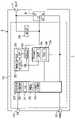
- FIG. 2 is a block circuit diagram showing the electrical structure of the semiconductor device.
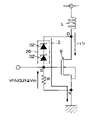
- FIG. 3 is a circuit diagram for explaining normal operation and active clamp operation of the semiconductor device.
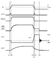
- FIG. 4 is a waveform diagram of main electrical signals.
- FIG. 5 is a cross-sectional perspective view of region V shown in FIG.
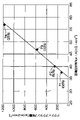
- FIG. 6 is a graph obtained by actually measuring the relationship between the active clamping capacity and the area resistivity.
- FIG. 7 is a cross-sectional perspective view for explaining normal operation of the semiconductor device.
- FIG. 8 is a cross-sectional perspective view for explaining the active clamping operation of the semiconductor device.
- FIG. 10 is an equivalent circuit diagram representing the power MISFET of FIG. 9 as a first MISFET and a second MISFET.
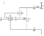
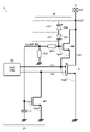
- 11 is a circuit diagram showing a configuration example of the gate control circuit and the active clamp circuit in FIG. 9.
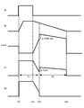
- FIG. 12 is a timing chart showing how the first Half-ON control of the power MISFET 9 is performed during the active clamp operation in the semiconductor device.
- FIG. 13 is a diagram for explaining the cause of output overshoot.
- FIG. 14 is a diagram showing how an output overshoot occurs.
- FIG. 15 is a diagram showing a second embodiment of the semiconductor device.
- FIG. 16 is a diagram showing how the output overshoot is suppressed.
- FIG. 17 is a diagram showing a semiconductor device according to a third embodiment.
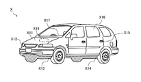
- FIG. 18 is an external view showing one configuration example of
- FIG. 1 is a perspective view of the semiconductor device 1 viewed from one direction. A mode example in which the semiconductor device 1 is a low-side switching device will be described below.
- semiconductor device 1 includes semiconductor layer 2 .
- the semiconductor layer 2 contains silicon.
- the semiconductor layer 2 is formed in the shape of a rectangular parallelepiped chip.
- the semiconductor layer 2 has a first main surface 3 on one side, a second main surface 4 on the other side, and side surfaces 5A, 5B, 5C, and 5D connecting the first main surface 3 and the second main surface 4. ing.
- the first main surface 3 and the second main surface 4 are formed in a quadrangular shape when viewed from the normal direction Z (hereinafter simply referred to as "plan view").
- the side surface 5A and the side surface 5C extend along the first direction X and face each other in a second direction Y intersecting the first direction X.
- the side surface 5B and the side surface 5D extend along the second direction Y and face each other in the first direction X.
- the second direction Y is, more specifically, orthogonal to the first direction X. As shown in FIG.
- An output area 6 and an input area 7 are set in the semiconductor layer 2 .
- the output area 6 is set in the area on the side of the side surface 5C.
- the input area 7 is set in the area on the side 5A side.
- the area SOUT of the output region 6 is greater than or equal to the area SIN of the input region 7 (SIN ⁇ SOUT).
- the ratio SOUT/SIN of the area SOUT to the area SIN may be 1 or more and 10 or less (1 ⁇ SOUT/SIN ⁇ 10).
- the ratio SOUT/SIN may be 1 or more and 2 or less, 2 or more and 4 or less, 4 or more and 6 or less, 6 or more and 8 or less, or 8 or more and 10 or less.
- the planar shape of the input area 7 and the planar shape of the output area 6 are arbitrary and are not limited to specific shapes. Of course, the ratio SOUT/SIN may be greater than 0 and less than 1.
- the output region 6 includes a power MISFET (Metal Insulator Semiconductor Field Effect Transistor) 9 as an example of an insulated gate power transistor.
- Power MISFET 9 includes a gate, drain and source.
- the input area 7 includes a control IC (Integrated Circuit) 10 as an example of a control circuit.
- the control IC 10 includes multiple types of functional circuits that implement various functions.
- the plurality of types of functional circuits include circuits that generate gate control signals for driving and controlling the power MISFET 9 based on electrical signals from the outside.
- the control IC 10 forms a so-called IPD (Intelligent Power Device) together with the power MISFET 9 .
- the IPD is also called an IPM (Intelligent Power Module).
- the input area 7 is electrically isolated from the output area 6 by the area isolation structure 8 .
- the region isolation structures 8 are indicated by hatching. Although a detailed description is omitted, the region isolation structure 8 may have a trench isolation structure in which a trench is filled with an insulator.
- a plurality of (three in this embodiment) electrodes 11 , 12 , 13 are formed on the semiconductor layer 2 .
- a plurality of electrodes 11-13 are indicated by hatching.
- a plurality of electrodes 11 to 13 are formed as terminal electrodes externally connected by conducting wires (eg, bonding wires) or the like.
- the number, arrangement and planar shape of the plurality of electrodes 11 to 13 are arbitrary, and are not limited to the form shown in FIG.
- the number, arrangement and planar shape of the plurality of electrodes 11 to 13 are adjusted according to the specifications of the power MISFET 9 and the specifications of the control IC 10.
- the plurality of electrodes 11-13 includes a drain electrode 11 (output electrode), a source electrode 12 (reference voltage electrode) and an input electrode 13 in this embodiment.
- the drain electrode 11 is formed on the second main surface 4 of the semiconductor layer 2 .
- the drain electrode 11 transmits an electric signal generated by the power MISFET 9 to the outside.
- the drain electrode 11 may include at least one of a Ti layer, Ni layer, Au layer, Ag layer and Al layer.
- the drain electrode 11 may have a single layer structure including a Ti layer, Ni layer, Au layer, Ag layer or Al layer.
- the drain electrode 11 may have a laminated structure in which at least two of a Ti layer, a Ni layer, an Au layer, an Ag layer, and an Al layer are laminated in an arbitrary manner.
- the source electrode 12 is formed on the output region 6 on the first main surface 3 .
- the source electrode 12 provides a reference voltage (for example, ground voltage) to various functional circuits of the power MISFET 9 and control IC 10 .
- the input electrode 13 is formed on the input area 7 on the first main surface 3 .
- Input electrode 13 transmits an input voltage for driving control IC 10 .
- a gate control wiring 17 as an example of a control wiring is further formed on the semiconductor layer 2 .
- the gate control wiring 17 is selectively routed to the output region 6 and the input region 7 .
- the gate control wiring 17 is electrically connected to the gate of the power MISFET 9 in the output region 6 and electrically connected to the control IC 10 in the input region 7 .
- the gate control wiring 17 transmits the gate control signal generated by the control IC 10 to the gate of the power MISFET 9 .
- the gate control signals include on-signal Von and off-signal Voff, and control the on-state and off-state of power MISFET 9 .
- the ON signal Von is higher than the gate threshold voltage Vth of the power MISFET 9 (Vth ⁇ Von).
- the off signal Voff is lower than the gate threshold voltage Vth of the power MISFET 9 (Voff ⁇ Vth).
- the off signal Voff may be a reference voltage (eg ground voltage).
- the gate control wiring 17 includes a first gate control wiring 17A, a second gate control wiring 17B and a third gate control wiring 17C in this form.
- the first gate control wiring 17A, the second gate control wiring 17B and the third gate control wiring 17C are electrically insulated from each other.
- two first gate control wirings 17A are routed to different regions. Also, the two second gate control wirings 17B are routed to different regions. Also, the two third gate control wirings 17C are routed to different regions.
- the first gate control wiring 17A, the second gate control wiring 17B and the third gate control wiring 17C transmit the same or different gate control signals to the gates of the power MISFETs 9.
- the number, arrangement, shape, etc. of the gate control wiring 17 are arbitrary, and are adjusted according to the transmission distance of the gate control signals and the number of gate control signals to be transmitted.
- the source electrode 12, the input electrode 13 and the gate control wiring 17 may each contain at least one of nickel, palladium, aluminum, copper, aluminum alloy and copper alloy.
- the source electrode 12, the input electrode 13, and the gate control wiring 17 are made of Al-Si-Cu (aluminum-silicon-copper) alloy, Al-Si (aluminum-silicon) alloy, and Al-Cu (aluminum-copper) alloy. At least one of them may be included.
- the source electrode 12, the input electrode 13, and the gate control wiring 17 may contain the same type of electrode material, or may contain different electrode materials.
- FIG. 2 is a block circuit diagram showing the electrical structure of the semiconductor device 1 shown in FIG. A case where the semiconductor device 1 is mounted on a vehicle will be described below as an example.
- the semiconductor device 1 includes a drain electrode 11 as an output electrode, a source electrode 12 as a reference voltage electrode, an input electrode 13, a gate control wiring 17, a power MISFET 9 and a control IC 10.
- the drain electrode 11 is electrically connected to the drain of the power MISFET 9. Drain electrode 11 is connected to a load.
- Source electrode 12 is electrically connected to the source of power MISFET 9 .
- Source electrode 12 provides a reference voltage to power MISFET 9 and control IC 10 .
- the input electrode 13 may be connected to an MCU [Micro Controller Unit], a DC/DC converter, an LDO [Low Drop Out], or the like. Input electrode 13 provides an input voltage to control IC 10 .
- a gate of the power MISFET 9 is connected to a control IC 10 (a gate control circuit 25 to be described later) via a gate control wiring 17 .
- the control IC 10 includes a current/voltage control circuit 23, a protection circuit 24, a gate control circuit 25 and an active clamp circuit 26 in this form.
- the current/voltage control circuit 23 is connected to the source electrode 12 , the input electrode 13 , the protection circuit 24 and the gate control circuit 25 .
- Current/voltage control circuit 23 generates various voltages according to the electrical signal from input electrode 13 and the electrical signal from protection circuit 24 .
- the current/voltage control circuit 23 includes a drive voltage generation circuit 30 , a first constant voltage generation circuit 31 , a second constant voltage generation circuit 32 and a reference voltage/reference current generation circuit 33 in this embodiment.
- the drive voltage generation circuit 30 generates a drive voltage for driving the gate control circuit 25 .
- a drive voltage generated by the drive voltage generation circuit 30 is input to the gate control circuit 25 .
- the first constant voltage generation circuit 31 generates a first constant voltage for driving the protection circuit 24.
- the first constant voltage generation circuit 31 may include a Zener diode and a regulator circuit.
- the first constant voltage may be 1 V or more and 5 V or less.
- the first constant voltage is input to protection circuit 24 (for example, overcurrent protection circuit 34).
- the second constant voltage generation circuit 32 generates a second constant voltage for driving the protection circuit 24.
- the second constant voltage generation circuit 32 may include a Zener diode and a regulator circuit.
- the second constant voltage may be 1 V or more and 5 V or less.
- the second constant voltage is input to protection circuit 24 (for example, overheat protection circuit 36).
- the reference voltage/reference current generation circuit 33 generates reference voltages and reference currents for various circuits.
- the reference voltage may be 1 V or more and 5 V or less.
- the reference current may be 1 mA or more and 1 A or less.
- the reference voltage and reference current are input to various circuits. If the various circuits include comparators, the reference voltage and reference current may be input to the comparators.
- the protection circuit 24 is connected to the current/voltage control circuit 23 , the gate control circuit 25 and the source of the power MISFET 9 .
- Protection circuit 24 includes an overcurrent protection circuit 34 and an overheat protection circuit 36 .
- the overcurrent protection circuit 34 protects the power MISFET 9 from overcurrent.
- the overcurrent protection circuit 34 is connected to the gate control circuit 25 .
- Overcurrent protection circuit 34 may include a current monitor circuit. A signal generated by the overcurrent protection circuit 34 is input to the gate control circuit 25 (more specifically, a drive signal output circuit 40 described later).
- the overheat protection circuit 36 protects the power MISFET 9 from excessive temperature rise.
- the overheat protection circuit 36 is connected to the current/voltage control circuit 23 .
- Overheat protection circuit 36 monitors the temperature of semiconductor device 1 .
- the overheat protection circuit 36 may include temperature sensitive devices such as temperature sensitive diodes and thermistors.
- a signal generated by the overheat protection circuit 36 is input to the current/voltage control circuit 23 .
- the gate control circuit 25 controls the ON state and OFF state of the power MISFET 9 .
- the gate control circuit 25 is connected to gates of the current/voltage control circuit 23 , the protection circuit 24 and the power MISFET 9 .
- the gate control circuit 25 generates a plurality of types of gate control signals according to the number of gate control wirings 17 according to the electric signal from the current/voltage control circuit 23 and the electric signal from the protection circuit 24 .
- a plurality of types of gate control signals are input to the gate of the power MISFET 9 via gate control wiring 17 .
- the gate control circuit 25 collectively controls a plurality of gate control signals in response to an electrical signal (input signal) applied to the input electrode 13 to turn on/off the power MISFET 9, while active clamping is performed. It has a function of individually controlling a plurality of gate control signals so as to raise the on-resistance of the power MISFET 9 when the circuit 26 operates (details will be described later).
- the gate control circuit 25 more specifically includes an oscillation circuit 38, a charge pump circuit 39 and a drive signal output circuit 40.
- the oscillator circuit 38 oscillates according to the electrical signal from the current/voltage control circuit 23 and generates a predetermined electrical signal.
- An electrical signal generated by the oscillator circuit 38 is input to the charge pump circuit 39 .
- the charge pump circuit 39 boosts the electric signal from the oscillation circuit 38 .
- the electric signal boosted by the charge pump circuit 39 is input to the drive signal output circuit 40 .
- the drive signal output circuit 40 generates a plurality of types of gate control signals according to the electrical signal from the charge pump circuit 39 and the electrical signal from the protection circuit 24 (more specifically, the overcurrent protection circuit 34).
- a plurality of types of gate control signals are input to the gate of the power MISFET 9 via gate control wiring 17 . Thereby, the power MISFET 9 is driven and controlled.
- the active clamp circuit 26 protects the power MISFET 9 from back electromotive force.
- the active clamp circuit 26 is connected to the drain electrode 11 and the gate of the power MISFET 9 .
- Active clamp circuit 26 may include multiple diodes.
- the active clamp circuit 26 may include multiple diodes forward-biased to each other. Active clamp circuit 26 may include multiple diodes that are reverse biased together. The active clamp circuit 26 may include multiple diodes forward biased together and multiple diodes reverse biased together.
- the plurality of diodes may include pn junction diodes, Zener diodes, or pn junction diodes and Zener diodes.
- Active clamp circuit 26 may include multiple Zener diodes biased together.
- Active clamp circuit 26 may include a Zener diode and a pn junction diode that are reverse biased together.
- FIG. 3 is a circuit diagram for explaining normal operation and active clamp operation of the semiconductor device 1 shown in FIG.
- FIG. 4 is a waveform diagram of main electrical signals applied to the circuit diagram shown in FIG.
- inductive load L is connected to the drain of the power MISFET 9.
- devices using windings (coils) such as solenoids, motors, transformers, and relays are exemplified as the inductive load L.
- Inductive load L is also referred to as L-load.
- the source of the power MISFET 9 is connected to the ground.
- a drain of the power MISFET 9 is electrically connected to an inductive load L.
- the gate and drain of power MISFET 9 are connected to active clamp circuit 26 .
- the gate and source of power MISFET 9 are connected to resistor R.
- the active clamp circuit 26 includes k (k is a natural number) Zener diodes DZ bias-connected to each other in this circuit example.
- the power MISFET 9 switches from the OFF state to the ON state (normal operation).
- the ON signal Von has a voltage equal to or higher than the gate threshold voltage Vth (Vth ⁇ Von).
- the power MISFET 9 is kept on for a predetermined on-time TON.
- the drain current ID begins to flow from the drain of the power MISFET 9 to the source.
- the drain current ID increases in proportion to the ON time TON of the power MISFET9.
- Inductive load L stores inductive energy due to the increase in drain current ID.
- the off signal Voff When the off signal Voff is input to the gate of the power MISFET 9, the power MISFET 9 switches from the on state to the off state.
- the off signal Voff has a voltage less than the gate threshold voltage Vth (Voff ⁇ Vth).
- the off signal Voff may be a reference voltage (eg ground voltage).
- the power MISFET 9 enters an active clamp state (active clamp operation).
- active clamp operation active clamp operation
- the drain voltage VDS rapidly rises to the clamp voltage VDSSCL.
- the power MISFET 9 is destroyed.
- the power MISFET 9 is designed so that the clamp voltage VDSSCL is equal to or less than the maximum rated drain voltage VDSS (VDSSCL ⁇ VDSS).
- the clamp voltage VDSSCL is equal to or lower than the maximum rated drain voltage VDSS (VDSSCL ⁇ VDSS)
- the reverse current IZ flows through the active clamp circuit 26.
- a limiting voltage VL is formed across the terminals of the active clamp circuit 26 .
- the reverse current IZ passes through the resistor R and reaches the ground.
- an inter-terminal voltage VR is formed between the terminals of the resistor R.
- the inter-terminal voltage VR is applied between the gate and source of the power MISFET 9 as a clamp-on voltage VCLP. Therefore, power MISFET 9 maintains the ON state in the active clamp state.
- the clamp-on voltage VCLP (inter-terminal voltage VR) may have a voltage less than the on-signal Von.
- the inductive energy of the inductive load L is consumed (absorbed) by the power MISFET 9.
- the drain current ID decreases from the peak value IAV just before the power MISFET 9 is turned off to zero after the active clamp time TAV.
- the gate voltage VGS becomes the ground voltage
- the drain voltage VDS becomes the power supply voltage VB
- the power MISFET 9 switches from the ON state to the OFF state.
- the active clamp tolerance Eac of the power MISFET 9 is defined by the tolerance during active clamp operation. More specifically, active clamp tolerance Eac is defined by the tolerance to back electromotive force caused by inductive energy of inductive load L when power MISFET 9 transitions from the ON state to the OFF state.
- the active clamp tolerance Eac is defined by the tolerance to energy caused by the clamp voltage VDSSCL, as clarified in the circuit example of FIG.
- the on-resistance and active clamp resistance are adjusted, for example, by the channel area of the transistor.
- the area of the channel is increased, the current path can be increased during normal operation, so the on-resistance can be reduced.
- the active clamp tolerance is lowered due to a rapid temperature rise caused by the back electromotive force during the active clamp operation.
- FIG. 5 is a cross-sectional perspective view of region V shown in FIG.
- the upper structure of the first main surface 3 (the source electrode 12, the gate control wiring 17, the interlayer insulating layer, etc.) is omitted in this figure.
- the semiconductor layer 2 has a laminated structure including an n + -type semiconductor substrate 51 and an n-type epitaxial layer 52 in this embodiment.
- a second main surface 4 of the semiconductor layer 2 is formed by the semiconductor substrate 51 .
- the epitaxial layer 52 forms the first main surface 3 of the semiconductor layer 2 .
- Semiconductor substrate 51 and epitaxial layer 52 form side surfaces 5A to 5D of semiconductor layer 2 .
- the epitaxial layer 52 has an n-type impurity concentration less than the n-type impurity concentration of the semiconductor substrate 51 .
- the n-type impurity concentration of the semiconductor substrate 51 may be 1 ⁇ 10 18 cm ⁇ 3 or more and 1 ⁇ 10 20 cm ⁇ 3 or less.
- the n-type impurity concentration of the epitaxial layer 52 may be 1 ⁇ 10 15 cm ⁇ 3 or more and 1 ⁇ 10 18 cm ⁇ 3 or less.
- the epitaxial layer 52 has a thickness Tepi less than the thickness Tsub of the semiconductor substrate 51 (Tepi ⁇ Tsub).
- the thickness Tsub may be 50 ⁇ m or more and 450 ⁇ m or less.
- the thickness Tsub may be 50 ⁇ m to 150 ⁇ m, 150 ⁇ m to 250 ⁇ m, 250 ⁇ m to 350 ⁇ m, or 350 ⁇ m to 450 ⁇ m.
- the resistance value can be reduced by reducing the thickness Tsub.
- the thickness Tsub is adjusted by grinding.
- the second main surface 4 of the semiconductor layer 2 may be a ground surface having grinding marks.
- the thickness Tepi of the epitaxial layer 52 is preferably 1/10 or less of the thickness Tsub.
- the thickness Tepi may be 5 ⁇ m or more and 20 ⁇ m or less.
- the thickness Tepi may be between 5 ⁇ m and 10 ⁇ m, between 10 ⁇ m and 15 ⁇ m, or between 15 ⁇ m and 20 ⁇ m.
- the thickness Tepi is preferably 5 ⁇ m or more and 15 ⁇ m or less.
- a semiconductor substrate 51 is formed on the second main surface 4 side of the semiconductor layer 2 as a drain region 53 .
- the epitaxial layer 52 is formed in the surface layer portion of the first main surface 3 of the semiconductor layer 2 as a drift region 54 (drain drift region).
- the bottom of drift region 54 is formed by the boundary of semiconductor substrate 51 and epitaxial layer 52 .
- the epitaxial layer 52 is hereinafter referred to as a drift region 54 .
- a p-type body region 55 is formed in the surface layer portion of the first main surface 3 of the semiconductor layer 2 in the output region 6 .
- the body region 55 is the base region of the power MISFET 9 .
- the body region 55 may have a p-type impurity concentration of 1 ⁇ 10 16 cm ⁇ 3 or more and 1 ⁇ 10 18 cm ⁇ 3 or less.
- the body region 55 is formed on the surface layer of the drift region 54 .
- the bottom of body region 55 is formed in a region on the first main surface 3 side with respect to the bottom of drift region 54 .
- the thickness of the body region 55 may be 0.5 ⁇ m or more and 2 ⁇ m or less.
- the thickness of the body region 55 may be 0.5 ⁇ m or more and 1 ⁇ m or less, 1 ⁇ m or more and 1.5 ⁇ m or less, or 1.5 ⁇ m or more and 2 ⁇ m or less.
- the power MISFET 9 includes a first MISFET 56 (first transistor) and a second MISFET 57 (second transistor).
- the first MISFET 56 is electrically isolated from the second MISFET 57 and independently controlled.
- the second MISFET 57 is electrically isolated from the first MISFET 56 and independently controlled.
- the power MISFET 9 is configured to be driven when both the first MISFET 56 and the second MISFET 57 are in the ON state (Full-ON control). Also, the power MISFET 9 is configured to be driven while the first MISFET 56 is in the ON state and the second MISFET 57 is in the OFF state (first Half-ON control). Furthermore, the power MISFET 9 is configured to be driven while the first MISFET 56 is in the OFF state and the second MISFET 57 is in the ON state (second Half-ON control).
- the power MISFET 9 In the case of Full-ON control, the power MISFET 9 is driven with all current paths released. Therefore, the on-resistance in the semiconductor layer 2 is relatively lowered. On the other hand, in the case of the first Half-ON control or the second Half-ON control, the power MISFET 9 is driven with some current paths cut off. Therefore, the on-resistance in the semiconductor layer 2 relatively increases.
- the first MISFET 56 specifically includes a plurality of first FET (Field Effect Transistor) structures 58 .
- the plurality of first FET structures 58 are arranged at intervals along the first direction X and extend along the second direction Y in a strip shape, respectively, in plan view.
- the plurality of first FET structures 58 are formed in a stripe shape as a whole in plan view.
- the region on the one end side of the first FET structure 58 is illustrated, and the illustration of the region on the other end side of the first FET structure 58 is omitted.
- the structure of the region on the other end side of the first FET structure 58 is substantially the same as the structure of the region on the one end side of the first FET structure 58 .
- the structure of the region on the one end side of the first FET structure 58 will be described as an example, and the structure of the region on the other end side of the first FET structure 58 will be omitted.
- Each first FET structure 58 includes a first trench gate structure 60 in this form.
- the first width WT1 of the first trench gate structure 60 may be between 0.5 ⁇ m and 5 ⁇ m.
- the first width WT1 is the width in the direction (first direction X) orthogonal to the direction (second direction Y) in which the first trench gate structure 60 extends.
- the first width WT1 is 0.5 ⁇ m or more and 1 ⁇ m or less, 1 ⁇ m or more and 1.5 ⁇ m or less, 1.5 ⁇ m or more and 2 ⁇ m or less, 2 ⁇ m or more and 2.5 ⁇ m or less, 2.5 ⁇ m or more and 3 ⁇ m or less, 3 ⁇ m or more and 3.5 ⁇ m or less, It may be 3.5 ⁇ m or more and 4 ⁇ m or less, 4 ⁇ m or more and 4.5 ⁇ m or less, or 4.5 ⁇ m or more and 5 ⁇ m or less.
- the first width WT1 is preferably 0.8 ⁇ m or more and 1.2 ⁇ m or less.
- the first trench gate structure 60 penetrates the body region 55 and reaches the drift region 54 .
- the first depth DT1 of the first trench gate structure 60 may be 1 ⁇ m or more and 10 ⁇ m or less.
- the first depth DT1 may be 1 ⁇ m or more and 2 ⁇ m or less, 2 ⁇ m or more and 4 ⁇ m or less, 4 ⁇ m or more and 6 ⁇ m or less, 6 ⁇ m or more and 8 ⁇ m or less, or 8 ⁇ m or more and 10 ⁇ m or less.
- the first depth DT1 is preferably 2 ⁇ m or more and 6 ⁇ m or less.
- the first trench gate structure 60 includes a first sidewall 61 on one side, a second sidewall 62 on the other side, and a bottom wall 63 connecting the first sidewall 61 and the second sidewall 62 .
- the 1st side wall 61, the 2nd side wall 62, and the bottom wall 63 may be collectively called an “inner wall” or an “outer wall.”
- the absolute value of the angle (taper angle) formed between the first side wall 61 and the first main surface 3 in the semiconductor layer 2 may be more than 90° and 95° or less (for example, about 91°).
- the absolute value of the angle (taper angle) formed between second sidewall 62 and first main surface 3 in semiconductor layer 2 may be more than 90° and 95° or less (for example, about 91°).
- the first trench gate structure 60 may be formed in a tapered shape (tapered shape) in which the first width WT1 narrows from the first main surface 3 side toward the bottom wall 63 side in a cross-sectional view.
- the bottom wall 63 of the first trench gate structure 60 is located in a region on the first main surface 3 side with respect to the bottom of the drift region 54 .
- a bottom wall 63 of the first trench gate structure 60 is formed in a convex curved shape (U-shape) toward the bottom of the drift region 54 .
- the bottom wall 63 of the first trench gate structure 60 is located in the region on the first main surface 3 side with a first interval IT1 of 1 ⁇ m or more and 10 ⁇ m or less from the bottom of the drift region 54 .
- the first interval IT1 may be 1 ⁇ m or more and 2 ⁇ m or less, 2 ⁇ m or more and 4 ⁇ m or less, 4 ⁇ m or more and 6 ⁇ m or less, 6 ⁇ m or more and 8 ⁇ m or less, or 8 ⁇ m or more and 10 ⁇ m or less.
- the first interval IT1 is preferably 1 ⁇ m or more and 5 ⁇ m or less.
- the second MISFET 57 includes a plurality of second FET structures 68 in this form.
- the plurality of second FET structures 68 are arranged at intervals along the first direction X and extend along the second direction Y in a strip shape, respectively, in plan view.
- the multiple second FET structures 68 extend along the same direction as the multiple first FET structures 58 .
- the plurality of second FET structures 68 are formed in a stripe shape as a whole in plan view.
- the plurality of second FET structures 68 are alternately arranged with the plurality of first FET structures 58 in a manner that sandwiches one first FET structure 58 in this embodiment.
- the region on the one end side of the second FET structure 68 is illustrated, and the illustration of the region on the other end side of the second FET structure 68 is omitted.
- the structure of the region on the other end side of the second FET structure 68 is substantially the same as the structure of the region on the one end side of the second FET structure 68 .
- the structure of the region on the one end side of the second FET structure 68 will be described as an example, and the structure of the region on the other end side of the second FET structure 68 will be omitted.
- Each second FET structure 68 includes a second trench gate structure 70 in this form.
- a second width WT2 of the second trench gate structure 70 may be 0.5 ⁇ m or more and 5 ⁇ m or less.
- the second width WT2 is the width in the direction (first direction X) orthogonal to the direction (second direction Y) in which the second trench gate structure 70 extends.
- the second width WT2 is 0.5 ⁇ m or more and 1 ⁇ m or less, 1 ⁇ m or more and 1.5 ⁇ m or less, 1.5 ⁇ m or more and 2 ⁇ m or less, 2 ⁇ m or more and 2.5 ⁇ m or less, 2.5 ⁇ m or more and 3 ⁇ m or less, 3 ⁇ m or more and 3.5 ⁇ m or less, It may be 3.5 ⁇ m or more and 4 ⁇ m or less, 4 ⁇ m or more and 4.5 ⁇ m or less, or 4.5 ⁇ m or more and 5 ⁇ m or less.
- the second width WT2 is preferably 0.8 ⁇ m or more and 1.2 ⁇ m or less.
- the second width WT2 of the second trench gate structure 70 may be greater than or equal to the first width WT1 of the first trench gate structure 60 (WT1 ⁇ WT2).
- the second width WT2 may be less than or equal to the first width WT1 (WT1 ⁇ WT2).
- the second trench gate structure 70 penetrates the body region 55 and reaches the drift region 54.
- the second depth DT2 of the second trench gate structure 70 may be 1 ⁇ m or more and 10 ⁇ m or less.
- the second depth DT2 may be 1 ⁇ m or more and 2 ⁇ m or less, 2 ⁇ m or more and 4 ⁇ m or less, 4 ⁇ m or more and 6 ⁇ m or less, 6 ⁇ m or more and 8 ⁇ m or less, or 8 ⁇ m or more and 10 ⁇ m or less.
- the second depth DT2 is preferably 2 ⁇ m or more and 6 ⁇ m or less.
- the second depth DT2 of the second trench gate structure 70 may be greater than or equal to the first depth DT1 of the first trench gate structure 60 (DT1 ⁇ DT2).
- the second depth DT2 may be less than or equal to the first depth DT1 (DT1 ⁇ DT2).
- the second trench gate structure 70 includes a first sidewall 71 on one side, a second sidewall 72 on the other side, and a bottom wall 73 connecting the first sidewall 71 and the second sidewall 72 .
- the 1st side wall 71, the 2nd side wall 72, and the bottom wall 73 may be collectively called an “inner wall” or an “outer wall.”
- the absolute value of the angle (taper angle) formed between the first sidewall 71 and the first main surface 3 in the semiconductor layer 2 may be more than 90° and 95° or less (for example, about 91°).
- the absolute value of the angle (taper angle) formed between second side wall 72 and first main surface 3 in semiconductor layer 2 may be more than 90° and 95° or less (for example, about 91°).
- the second trench gate structure 70 may be formed in a tapered shape (tapered shape) in which the second width WT2 narrows from the first main surface 3 side toward the bottom wall 73 side in a cross-sectional view.
- the bottom wall 73 of the second trench gate structure 70 is located in a region on the first main surface 3 side with respect to the bottom of the drift region 54 .
- a bottom wall 73 of the second trench gate structure 70 is formed in a convex curved shape (U-shape) toward the bottom of the drift region 54 .
- the bottom wall 73 of the second trench gate structure 70 is located in the region on the first main surface 3 side with a second distance IT2 of 1 ⁇ m or more and 10 ⁇ m or less from the bottom of the drift region 54 .
- the second interval IT2 may be 1 ⁇ m or more and 2 ⁇ m or less, 2 ⁇ m or more and 4 ⁇ m or less, 4 ⁇ m or more and 6 ⁇ m or less, 6 ⁇ m or more and 8 ⁇ m or less, or 8 ⁇ m or more and 10 ⁇ m or less.
- the second interval IT2 is preferably 1 ⁇ m or more and 5 ⁇ m or less.
- a cell region 75 is defined in each region between the plurality of first trench gate structures 60 and the plurality of second trench gate structures 70 .
- the plurality of cell regions 75 are arranged at intervals along the first direction X in a plan view, and each extend in a band shape along the second direction Y. As shown in FIG.
- a plurality of cell regions 75 extend along the same direction as the first trench gate structure 60 and the second trench gate structure 70 .
- the plurality of cell regions 75 are formed in a stripe shape as a whole in plan view.
- a first depletion layer extends into the drift region 54 from the outer wall of the first trench gate structure 60 .
- the first depletion layer extends from the outer wall of the first trench gate structure 60 in the direction along the first main surface 3 and the normal direction Z.
- a second depletion layer extends into the drift region 54 from the outer wall of the second trench gate structure 70 .
- the second depletion layer extends from the outer wall of the second trench gate structure 70 in the direction along the first main surface 3 and the normal direction Z.
- the second trench gate structure 70 is spaced apart from the first trench gate structure 60 in such a manner that the second depletion layer overlaps the first depletion layer. That is, the second depletion layer overlaps the first depletion layer in the cell region 75 in the region on the first main surface 3 side with respect to the bottom wall 73 of the second trench gate structure 70 . According to such a structure, it is possible to suppress the electric field from concentrating on the first trench gate structure 60 and the second trench gate structure 70, thereby suppressing a decrease in the breakdown voltage.
- the second depletion layer preferably overlaps the first depletion layer in a region on the bottom side of the drift region 54 with respect to the bottom wall 73 of the second trench gate structure 70 . According to such a structure, concentration of an electric field on the bottom wall 63 of the first trench gate structure 60 and the bottom wall 73 of the second trench gate structure 70 can be suppressed, so that a decrease in breakdown voltage can be suppressed appropriately. .
- the pitch PS between sidewalls of the first trench gate structure 60 and the second trench gate structure 70 may be 0.2 ⁇ m or more and 2 ⁇ m or less.
- the pitch PS is between the first sidewall 61 (second sidewall 62) of the first trench gate structure 60 and the second sidewall 72 (first sidewall 71) of the second trench gate structure 70 between the first trench gate structure 60 and It is the distance in the direction (first direction X) orthogonal to the direction (second direction Y) in which the second trench gate structure 70 extends.
- the pitch PS is 0.2 ⁇ m or more and 0.4 ⁇ m or less, 0.4 ⁇ m or more and 0.6 ⁇ m or less, 0.6 ⁇ m or more and 0.8 ⁇ m or less, 0.8 ⁇ m or more and 1.0 ⁇ m or less, 1.0 ⁇ m or more and 1.2 ⁇ m or less, 1 2 ⁇ m or more and 1.4 ⁇ m or less, 1.4 ⁇ m or more and 1.6 ⁇ m or less, 1.6 ⁇ m or more and 1.8 ⁇ m or less, or 1.8 ⁇ m or more and 2.0 ⁇ m or less.
- the pitch PS is preferably 0.3 ⁇ m or more and 1.5 ⁇ m or less.
- the pitch PC between the central portions of the first trench gate structure 60 and the second trench gate structure 70 may be 1 ⁇ m or more and 7 ⁇ m or less.
- the pitch PC is in the direction in which the first trench gate structure 60 and the second trench gate structure 70 extend (the second direction Y) between the central portion of the first trench gate structure 60 and the central portion of the second trench gate structure 70. It is the distance in the orthogonal direction (first direction X).
- the pitch PC may be 1 ⁇ m or more and 2 ⁇ m or less, 2 ⁇ m or more and 3 ⁇ m or less, 3 ⁇ m or more and 4 ⁇ m or less, 4 ⁇ m or more and 5 ⁇ m or less, 5 ⁇ m or more and 6 ⁇ m or less, or 6 ⁇ m or more and 7 ⁇ m or less.
- the pitch PC is preferably 1 ⁇ m or more and 3 ⁇ m or less.
- the first trench gate structure 60 more specifically includes a first gate trench 81 , a first insulating layer 82 and a first electrode 83 .
- the first gate trench 81 is formed by digging the first main surface 3 toward the second main surface 4 side.
- the first gate trench 81 defines a first sidewall 61 , a second sidewall 62 and a bottom wall 63 of the first trench gate structure 60 .
- the first sidewall 61 , the second sidewall 62 and the bottom wall 63 of the first trench gate structure 60 are hereinafter also referred to as the first sidewall 61 , the second sidewall 62 and the bottom wall 63 of the first gate trench 81 .
- the first insulating layer 82 is formed like a film along the inner wall of the first gate trench 81 .
- the first insulating layer 82 defines a recessed space within the first gate trench 81 .
- a portion of the first insulating layer 82 covering the bottom wall 63 of the first gate trench 81 is formed along the bottom wall 63 of the first gate trench 81 .
- the first insulating layer 82 defines a U-shaped space recessed in a U-shape in the first gate trench 81 .
- the first insulating layer 82 is at least one of silicon oxide (SiO 2 ), silicon nitride (SiN), aluminum oxide (Al 2 O 3 ), zirconium oxide (ZrO 2 ), and tantalum oxide (Ta 2 O 3 ). including.
- the first insulating layer 82 may have a laminated structure including a SiN layer and a SiO 2 layer laminated in this order from the semiconductor layer 2 side.
- the first insulating layer 82 may have a laminated structure including a SiO 2 layer and a SiN layer laminated in this order from the semiconductor layer 2 side.
- the first insulating layer 82 may have a single layer structure consisting of a SiO2 layer or a SiN layer.
- the first insulating layer 82 has a single-layer structure consisting of a SiO 2 layer in this embodiment.
- the first insulating layer 82 includes a first bottom-side insulating layer 84 and a first opening-side insulating layer 85 formed in this order from the bottom wall 63 side of the first gate trench 81 toward the first main surface 3 side.
- the first bottom-side insulating layer 84 covers the inner wall of the first gate trench 81 on the bottom wall 63 side. More specifically, the first bottom-side insulating layer 84 covers the inner wall of the first gate trench 81 on the bottom wall 63 side with respect to the bottom of the body region 55 .
- the first bottom insulating layer 84 defines a U-shaped space on the bottom wall 63 side of the first gate trench 81 .
- the first bottom insulating layer 84 has a smooth inner wall surface defining a U-shaped space.
- a first bottom insulating layer 84 contacts the drift region 54 .
- a portion of the first bottom insulating layer 84 may contact the body region 55 .
- the first opening side insulating layer 85 covers the inner wall of the first gate trench 81 on the opening side. More specifically, the first opening side insulating layer 85 covers the first sidewall 61 and the second sidewall 62 of the first gate trench 81 in the region on the opening side of the first gate trench 81 with respect to the bottom of the body region 55 . covered. The first opening side insulating layer 85 is in contact with the body region 55 . A portion of the first opening side insulating layer 85 may be in contact with the drift region 54 .
- the first bottom insulating layer 84 has a first thickness T1.
- the first opening side insulating layer 85 has a second thickness T2 (T2 ⁇ T1) less than the first thickness T1.
- the first thickness T1 is the thickness along the normal direction of the inner wall of the first gate trench 81 in the first bottom-side insulating layer 84 .
- the second thickness T2 is the thickness along the normal direction of the inner wall of the first gate trench 81 in the first opening side insulating layer 85 .
- the first ratio T1/WT1 of the first thickness T1 to the first width WT1 of the first gate trench 81 may be 0.1 or more and 0.4 or less.
- the first ratio T1/WT1 is 0.1 or more and 0.15 or less, 0.15 or more and 0.2 or less, 0.2 or more and 0.25 or less, 0.25 or more and 0.3 or less, or 0.3 or more. It may be 0.35 or less, or 0.35 or more and 0.4 or less.
- the first ratio T1/WT1 is preferably 0.25 or more and 0.35 or less.
- the first thickness T1 of the first bottom-side insulating layer 84 may be 1500 ⁇ or more and 4000 ⁇ or less.
- the first thickness T1 may be 1500 ⁇ to 2000 ⁇ , 2000 ⁇ to 2500 ⁇ , 2500 ⁇ to 3000 ⁇ , 3000 ⁇ to 3500 ⁇ , or 3500 ⁇ to 4000 ⁇ .
- the first thickness T1 is preferably 1800 ⁇ or more and 3500 ⁇ or less.
- the first thickness T1 may be adjusted to 4000 ⁇ or more and 12000 ⁇ or less according to the first width WT1 of the first gate trench 81 .
- the first thickness T1 is 4000 ⁇ to 5000 ⁇ , 5000 ⁇ to 6000 ⁇ , 6000 ⁇ to 7000 ⁇ , 7000 ⁇ to 8000 ⁇ , 8000 ⁇ to 9000 ⁇ , 9000 ⁇ to 10000 ⁇ , 10000 ⁇ to 11000 ⁇ , or 11000 ⁇ to 12000 ⁇ .
- the breakdown voltage of the semiconductor device 1 can be increased by increasing the thickness of the first bottom-side insulating layer 84 .
- the second thickness T2 of the first opening-side insulating layer 85 may be 1/100 or more and 1/10 or less of the first thickness T1 of the first bottom-side insulating layer 84 .
- the second thickness T2 may range from 100 ⁇ to 500 ⁇ .
- the second thickness T2 may be 100 ⁇ to 200 ⁇ , 200 ⁇ to 300 ⁇ , 300 ⁇ to 400 ⁇ , or 400 ⁇ to 500 ⁇ .
- the second thickness T2 is preferably 200 ⁇ or more and 400 ⁇ or less.
- the first bottom-side insulating layer 84 has a first thickness T1 from a portion covering the first sidewall 61 and the second sidewall 62 of the first gate trench 81 toward a portion covering the bottom wall 63 of the first gate trench 81 . is formed in a manner of decreasing.
- the thickness of the portion of the first bottom-side insulating layer 84 covering the bottom wall 63 of the first gate trench 81 is such that the thickness of the first bottom-side insulating layer 84 covers the first side wall 61 and the second side wall 62 of the first gate trench 81 . Less than the thickness of the part to be covered.
- the width of the opening on the bottom wall side of the U-shaped space partitioned by the first bottom-side insulating layer 84 is expanded by the reduction of the first thickness T1. This suppresses the tapering of the U-shaped space.
- Such a U-shaped space is formed, for example, by etching the inner wall of the first bottom-side insulating layer 84 (for example, wet etching).
- the first electrode 83 is embedded in the first gate trench 81 with the first insulating layer 82 interposed therebetween.
- a first gate control signal (first control signal) including an ON signal Von and an OFF signal Voff is applied to the first electrode 83 .
- the first electrode 83 in this embodiment has an isolation split electrode structure including a first bottom electrode 86 , a first opening electrode 87 and a first intermediate insulating layer 88 .
- the first bottom electrode 86 is buried on the bottom wall 63 side of the first gate trench 81 with the first insulating layer 82 interposed therebetween. More specifically, the first bottom-side electrode 86 is buried on the bottom wall 63 side of the first gate trench 81 with the first bottom-side insulating layer 84 interposed therebetween. The first bottom-side electrode 86 faces the drift region 54 with the first bottom-side insulating layer 84 interposed therebetween. A portion of the first bottom electrode 86 may face the body region 55 with the first bottom insulating layer 84 interposed therebetween.
- the first bottom-side electrode 86 defines a recess having an inverted concave shape in a cross-sectional view between the first bottom-side insulating layer 84 and the first opening-side insulating layer 85 on the opening side of the first gate trench 81 . .
- local electric field concentration on the first bottom electrode 86 can be suppressed, so that a decrease in breakdown voltage can be suppressed.
- the first bottom electrode 86 is tapered from the top end to the bottom end. It can be suppressed appropriately. Thereby, local electric field concentration on the lower end portion of the first bottom electrode 86 can be appropriately suppressed.
- the first bottom electrode 86 may include at least one of conductive polysilicon, tungsten, aluminum, copper, aluminum alloys and copper alloys.
- First bottom electrode 86 comprises conductive polysilicon in this form.
- the conductive polysilicon may contain n-type impurities or p-type impurities.
- the conductive polysilicon preferably contains n-type impurities.
- the first opening side electrode 87 is embedded in the opening side of the first gate trench 81 with the first insulating layer 82 interposed therebetween. More specifically, the first opening-side electrode 87 is embedded in an inverted concave recess defined on the opening side of the first gate trench 81 with the first opening-side insulating layer 85 interposed therebetween. The first opening-side electrode 87 faces the body region 55 with the first opening-side insulating layer 85 interposed therebetween. A portion of the first opening-side electrode 87 may face the drift region 54 with the first opening-side insulating layer 85 interposed therebetween.
- the first opening side electrode 87 may contain at least one of conductive polysilicon, tungsten, aluminum, copper, aluminum alloy and copper alloy.
- the first aperture side electrode 87 preferably comprises the same type of conductive material as the first bottom side electrode 86 .
- the first opening-side electrode 87 contains conductive polysilicon in this form.
- the conductive polysilicon may contain n-type impurities or p-type impurities.
- the conductive polysilicon preferably contains n-type impurities.
- the first intermediate insulating layer 88 is interposed between the first bottom-side electrode 86 and the first opening-side electrode 87 and electrically insulates the first bottom-side electrode 86 and the first opening-side electrode 87 . More specifically, the first intermediate insulating layer 88 covers the first bottom-side electrode 86 exposed from the first bottom-side insulating layer 84 in the region between the first bottom-side electrode 86 and the first opening-side electrode 87. is doing. A first intermediate insulating layer 88 covers the upper end (more specifically, the protrusion) of the first bottom electrode 86 . The first intermediate insulating layer 88 is continuous with the first insulating layer 82 (the first bottom side insulating layer 84).
- the first intermediate insulating layer 88 has a third thickness T3.
- the third thickness T3 is less than the first thickness T1 of the first bottom insulating layer 84 (T3 ⁇ T1).
- the third thickness T3 may be 1/100 or more and 1/10 or less of the first thickness T1.
- the third thickness T3 may range from 100 ⁇ to 500 ⁇ .
- the third thickness T3 may be 100 ⁇ to 200 ⁇ , 200 ⁇ to 300 ⁇ , 300 ⁇ to 400 ⁇ , or 400 ⁇ to 500 ⁇ .
- the third thickness T3 is preferably 200 ⁇ or more and 400 ⁇ or less.
- the first intermediate insulating layer 88 is made of at least one of silicon oxide (SiO 2 ), silicon nitride (SiN), aluminum oxide (Al 2 O 3 ), zirconium oxide (ZrO 2 ), and tantalum oxide (Ta 2 O 3 ). Contains seeds.
- the first intermediate insulating layer 88 has a single layer structure consisting of a SiO 2 layer in this embodiment.
- the exposed portion of the first opening side electrode 87 exposed from the first gate trench 81 is positioned on the bottom wall 63 side of the first gate trench 81 with respect to the first main surface 3 in this embodiment.
- the exposed portion of the first opening side electrode 87 is curved toward the bottom wall 63 of the first gate trench 81 .
- the exposed portion of the first opening side electrode 87 is covered with a first cap insulating layer formed in a film shape.
- the first cap insulating layer continues to the first insulating layer 82 (first opening side insulating layer 85 ) in the first gate trench 81 .
- the first cap insulating layer may contain silicon oxide (SiO 2 ).
- Each first FET structure 58 further includes a p-type first channel region 91 (first channel).
- the first channel region 91 is formed in a region of the body region 55 facing the first electrode 83 (first opening side electrode 87) with the first insulating layer 82 (first opening side insulating layer 85) interposed therebetween.
- the first channel region 91 is formed along the first sidewall 61 or the second sidewall 62 or the first sidewall 61 and the second sidewall 62 of the first trench gate structure 60 .
- the first channel region 91 is formed along the first sidewall 61 and the second sidewall 62 of the first trench gate structure 60 in this embodiment.
- Each first FET structure 58 further includes an n + -type first source region 92 formed in the surface layer of the body region 55 .
- First source region 92 defines a first channel region 91 in body region 55 with drift region 54 .
- the n-type impurity concentration of the first source region 92 exceeds the n-type impurity concentration of the drift region 54 .
- the n-type impurity concentration of the first source region 92 may be 1 ⁇ 10 19 cm ⁇ 3 or more and 1 ⁇ 10 21 cm ⁇ 3 or less.
- Each first FET structure 58 includes a plurality of first source regions 92 in this form.
- a plurality of first source regions 92 are formed at intervals along the first trench gate structure 60 in the surface layer portion of the body region 55 . More specifically, the plurality of first source regions 92 are formed along the first sidewall 61 or the second sidewall 62, or the first sidewall 61 and the second sidewall 62 of the first trench gate structure 60. .
- a plurality of first source regions 92 are spaced along first sidewall 61 and second sidewall 62 of first trench gate structure 60 in this configuration.
- the bottoms of the plurality of first source regions 92 are located in a region on the first main surface 3 side with respect to the bottoms of the body regions 55 .
- the plurality of first source regions 92 face the first electrode 83 (first opening side electrode 87) with the first insulating layer 82 (first opening side insulating layer 85) interposed therebetween.
- the first channel region 91 of the first MISFET 56 is formed in the body region 55 sandwiched between the plurality of first source regions 92 and the drift region 54 .
- Each first FET structure 58 further includes a p + -type first contact region 93 formed in the surface layer of the body region 55 .
- the p-type impurity concentration of the first contact region 93 exceeds the p-type impurity concentration of the body region 55 .
- the p-type impurity concentration of the first contact region 93 may be, for example, 1 ⁇ 10 19 cm ⁇ 3 or more and 1 ⁇ 10 21 cm ⁇ 3 or less.
- Each first FET structure 58 includes a plurality of first contact regions 93 in this form.
- a plurality of first contact regions 93 are formed at intervals along the first trench gate structure 60 in the surface layer portion of the body region 55 . More specifically, the plurality of first contact regions 93 are formed along the first sidewall 61 or the second sidewall 62, or the first sidewall 61 and the second sidewall 62 of the first trench gate structure 60. .
- a plurality of first contact regions 93 are spaced apart along the first sidewall 61 and the second sidewall 62 of the first trench gate structure 60 in this embodiment. More specifically, the multiple first contact regions 93 are formed in the surface layer portion of the body region 55 in an alternate arrangement with respect to the multiple first source regions 92 . The bottoms of the plurality of first contact regions 93 are located in a region on the first main surface 3 side with respect to the bottoms of the body regions 55 .
- a second trench gate structure 70 includes a second gate trench 101 , a second insulating layer 102 and a second electrode 103 .
- the second gate trench 101 is formed by digging the first main surface 3 toward the second main surface 4 side.
- the second gate trench 101 defines a first sidewall 71 , a second sidewall 72 and a bottom wall 73 of the second trench gate structure 70 .
- the first sidewall 71 , the second sidewall 72 and the bottom wall 73 of the second trench gate structure 70 are hereinafter also referred to as the first sidewall 71 , the second sidewall 72 and the bottom wall 73 of the second gate trench 101 .
- the second insulating layer 102 is formed like a film along the inner wall of the second gate trench 101 .
- the second insulating layer 102 defines a recessed space within the second gate trench 101 .
- a portion of the second insulating layer 102 covering the bottom wall 73 of the second gate trench 101 is formed along the bottom wall 73 of the second gate trench 101 .
- the second insulating layer 102 defines a U-shaped space recessed in a U-shape inside the second gate trench 101 .
- the second insulating layer 102 is at least one of silicon oxide (SiO 2 ), silicon nitride (SiN), aluminum oxide (Al 2 O 3 ), zirconium oxide (ZrO 2 ), and tantalum oxide (Ta 2 O 3 ). including.
- the second insulating layer 102 may have a laminated structure including a SiN layer and a SiO 2 layer laminated in this order from the semiconductor layer 2 side.
- the second insulating layer 102 may have a laminated structure including a SiO 2 layer and a SiN layer laminated in this order from the semiconductor layer 2 side.
- the second insulating layer 102 may have a single layer structure consisting of a SiO2 layer or a SiN layer.
- the second insulating layer 102 has a single layer structure consisting of a SiO 2 layer in this embodiment.
- the second insulating layer 102 includes a second bottom side insulating layer 104 and a second opening side insulating layer 105 formed in this order from the bottom wall 73 side of the second gate trench 101 toward the first main surface 3 side.
- the second bottom-side insulating layer 104 covers the inner wall of the second gate trench 101 on the bottom wall 73 side. More specifically, the second bottom-side insulating layer 104 covers the inner wall of the second gate trench 101 on the bottom wall 73 side with respect to the bottom of the body region 55 .
- the second bottom-side insulating layer 104 defines a U-shaped space on the bottom wall 73 side of the second gate trench 101 .
- the second bottom insulating layer 104 has a smooth inner wall surface defining a U-shaped space.
- a second bottom insulating layer 104 contacts the drift region 54 .
- a portion of the second bottom insulating layer 104 may contact the body region 55 .
- the second opening side insulating layer 105 covers the opening side inner wall of the second gate trench 101 . More specifically, the second opening-side insulating layer 105 covers the first sidewall 71 and the second sidewall 72 of the second gate trench 101 in the region on the opening side of the second gate trench 101 with respect to the bottom of the body region 55 . covered. The second opening side insulating layer 105 is in contact with the body region 55 . A portion of the second opening side insulating layer 105 may be in contact with the drift region 54 .
- the second bottom insulating layer 104 has a fourth thickness T4.
- the second opening side insulating layer 105 has a fifth thickness T5 (T5 ⁇ T4) less than the fourth thickness T4.
- the fourth thickness T4 is the thickness along the normal direction of the inner wall of the second gate trench 101 in the second bottom side insulating layer 104 .
- the fifth thickness T5 is the thickness along the normal direction of the inner wall of the second gate trench 101 in the second opening side insulating layer 105 .
- a second ratio T4/WT2 of the fourth thickness T4 to the second width WT2 of the second gate trench 101 may be 0.1 or more and 0.4 or less.
- the second ratio T4/WT2 is 0.1 or more and 0.15 or less, 0.15 or more and 0.2 or less, 0.2 or more and 0.25 or less, 0.25 or more and 0.3 or less, or 0.3 or more. It may be 0.35 or less, or 0.35 or more and 0.4 or less.
- the second ratio T4/WT2 is preferably 0.25 or more and 0.35 or less.
- the second ratio T4/WT2 may be less than or equal to the first ratio T1/WT1 (T4/WT2 ⁇ T1/WT1).
- the second ratio T4/WT2 may be greater than or equal to the first ratio T1/WT1 (T4/WT2 ⁇ T1/WT1).
- the fourth thickness T4 of the second bottom-side insulating layer 104 may be 1500 ⁇ or more and 4000 ⁇ or less.
- the fourth thickness T4 may be 1500 ⁇ to 2000 ⁇ , 2000 ⁇ to 2500 ⁇ , 2500 ⁇ to 3000 ⁇ , 3000 ⁇ to 3500 ⁇ , or 3500 ⁇ to 4000 ⁇ .
- the fourth thickness T4 is preferably 1800 ⁇ or more and 3500 ⁇ or less.
- the fourth thickness T4 may be 4000 ⁇ or more and 12000 ⁇ or less depending on the second width WT2 of the second gate trench 101 .
- the fourth thickness T4 is 4000 ⁇ to 5000 ⁇ , 5000 ⁇ to 6000 ⁇ , 6000 ⁇ to 7000 ⁇ , 7000 ⁇ to 8000 ⁇ , 8000 ⁇ to 9000 ⁇ , 9000 ⁇ to 10000 ⁇ , 10000 ⁇ to 11000 ⁇ , or 11000 ⁇ to 12000 ⁇ .
- the breakdown voltage of the semiconductor device 1 can be increased by thickening the second bottom-side insulating layer 104 .
- the fourth thickness T4 may be equal to or less than the first thickness T1 (T4 ⁇ T1).
- the fourth thickness T4 may be greater than or equal to the first thickness T1 (T4 ⁇ T1).
- the fifth thickness T5 of the second opening-side insulating layer 105 is less than the fourth thickness T4 of the second bottom-side insulating layer 104 (T5 ⁇ T4).
- the fifth thickness T5 may be 1/100 or more and 1/10 or less of the fourth thickness T4. It may be 100 ⁇ or more and 500 ⁇ or less.
- the fifth thickness T5 may be 100 ⁇ to 200 ⁇ , 200 ⁇ to 300 ⁇ , 300 ⁇ to 400 ⁇ , or 400 ⁇ to 500 ⁇ .
- the fifth thickness T5 is preferably 200 ⁇ or more and 400 ⁇ or less.
- the fifth thickness T5 may be equal to or less than the second thickness T2 (T5 ⁇ T2).
- the fifth thickness T5 may be greater than or equal to the second thickness T2 (T5 ⁇ T2).
- Second bottom-side insulating layer 104 has a fourth thickness T4 from a portion covering first sidewall 71 and second sidewall 72 of second gate trench 101 to a portion covering bottom wall 73 of second gate trench 101 . is formed in a manner of decreasing.
- the thickness of the portion of the second bottom-side insulating layer 104 covering the bottom wall 73 of the second gate trench 101 is such that the thickness of the second bottom-side insulating layer 104 covers the first side wall 71 and the second side wall 72 of the second gate trench 101 . Less than the thickness of the part to be covered.
- the width of the opening on the bottom wall side of the U-shaped space defined by the second bottom-side insulating layer 104 is expanded by the reduction of the fourth thickness T4. This suppresses the tapering of the U-shaped space.
- Such a U-shaped space is formed, for example, by etching the inner wall of the second bottom-side insulating layer 104 (for example, wet etching).
- the second electrode 103 is embedded in the second gate trench 101 with the second insulating layer 102 interposed therebetween.
- a predetermined second gate control signal (second control signal) including an ON signal Von and an OFF signal Voff is applied to the second electrode 103 .
- the second electrode 103 has, in this form, an insulation isolation type split electrode structure including a second bottom electrode 106, a second opening side electrode 107 and a second intermediate insulating layer .
- the second bottom electrode 106 is electrically connected to the first bottom electrode 86 in this configuration.
- the second aperture-side electrode 107 is electrically insulated from the first aperture-side electrode 87 .
- the second bottom electrode 106 is buried on the bottom wall 73 side of the second gate trench 101 with the second insulating layer 102 interposed therebetween. More specifically, the second bottom-side electrode 106 is buried on the bottom wall 73 side of the second gate trench 101 with the second bottom-side insulating layer 104 interposed therebetween. The second bottom-side electrode 106 faces the drift region 54 with the second bottom-side insulating layer 104 interposed therebetween. A portion of the second bottom-side electrode 106 may face the body region 55 with the second bottom-side insulating layer 104 interposed therebetween.
- the second bottom-side electrode 106 defines a recess having an inverted concave shape in a cross-sectional view between the second bottom-side insulating layer 104 and the second opening-side insulating layer 105 on the opening side of the second gate trench 101 . .
- local electric field concentration on the second bottom-side electrode 106 can be suppressed, so a decrease in breakdown voltage can be suppressed.
- the second bottom electrode 106 is tapered from the top end to the bottom end. It can be suppressed appropriately. As a result, local electric field concentration on the lower end portion of the second bottom electrode 106 can be appropriately suppressed.
- the second bottom electrode 106 may include at least one of conductive polysilicon, tungsten, aluminum, copper, aluminum alloys and copper alloys.
- the second bottom electrode 106 comprises conductive polysilicon in this form.
- the conductive polysilicon may contain n-type impurities or p-type impurities.
- the conductive polysilicon preferably contains n-type impurities.
- the second opening side electrode 107 is embedded in the opening side of the second gate trench 101 with the second insulating layer 102 interposed therebetween. More specifically, the second opening-side electrode 107 is embedded in an inverted concave recess defined on the opening side of the second gate trench 101 with the second opening-side insulating layer 105 interposed therebetween. The second opening-side electrode 107 faces the body region 55 with the second opening-side insulating layer 105 interposed therebetween. A portion of the second opening-side electrode 107 may face the drift region 54 with the second opening-side insulating layer 105 interposed therebetween.
- the second opening side electrode 107 may contain at least one of conductive polysilicon, tungsten, aluminum, copper, aluminum alloy and copper alloy.
- the second aperture side electrode 107 preferably comprises the same type of conductive material as the second bottom side electrode 106 .
- the second opening side electrode 107 contains conductive polysilicon in this form.
- the conductive polysilicon may contain n-type impurities or p-type impurities.
- the conductive polysilicon preferably contains n-type impurities.
- the second intermediate insulating layer 108 is interposed between the second bottom-side electrode 106 and the second opening-side electrode 107 to electrically insulate the second bottom-side electrode 106 and the second opening-side electrode 107 .
- the second intermediate insulating layer 108 more specifically covers the second bottom side electrode 106 exposed from the second bottom side insulating layer 104 in the region between the second bottom side electrode 106 and the second opening side electrode 107. is doing.
- a second intermediate insulating layer 108 covers the upper end (more specifically, the protrusion) of the second bottom electrode 106 .
- the second intermediate insulating layer 108 is continuous with the second insulating layer 102 (second bottom side insulating layer 104).
- the second intermediate insulating layer 108 has a sixth thickness T6.
- the sixth thickness T6 is less than the fourth thickness T4 of the second bottom insulating layer 104 (T6 ⁇ T4).
- the sixth thickness T6 may be 1/100 or more and 1/10 or less of the fourth thickness T4.
- the sixth thickness T6 may range from 100 ⁇ to 500 ⁇ .
- the sixth thickness T6 may be 100 ⁇ to 200 ⁇ , 200 ⁇ to 300 ⁇ , 300 ⁇ to 400 ⁇ , or 400 ⁇ to 500 ⁇ .
- the sixth thickness T6 is preferably 200 ⁇ or more and 400 ⁇ or less.
- the sixth thickness T6 may be less than or equal to the third thickness T3 (T6 ⁇ T3).
- the sixth thickness T6 may be greater than or equal to the third thickness T3 (T6 ⁇ T3).
- the second intermediate insulating layer 108 is at least one of silicon oxide (SiO 2 ), silicon nitride (SiN), aluminum oxide (Al 2 O 3 ), zirconium oxide (ZrO 2 ) and tantalum oxide (Ta 2 O 3 ). Contains seeds. It should be noted that the second intermediate insulating layer 108 has a single layer structure consisting of a SiO 2 layer in this embodiment.
- the exposed portion of the second opening side electrode 107 exposed from the second gate trench 101 is positioned on the bottom wall 73 side of the second gate trench 101 with respect to the first main surface 3 in this embodiment.
- the exposed portion of the second opening side electrode 107 is curved toward the bottom wall 73 of the second gate trench 101 .
- the exposed portion of the second opening side electrode 107 is covered with a second cap insulating layer formed in a film shape.
- the second cap insulating layer continues to the second insulating layer 102 (second opening side insulating layer 105 ) in the second gate trench 101 .
- the second cap insulating layer may contain silicon oxide (SiO 2 ).
- Each second FET structure 68 further includes a p-type second channel region 111 (second channel). More specifically, the second channel region 111 is a region facing the second electrode 103 (second opening side electrode 107) with the second insulating layer 102 (second opening side insulating layer 105) interposed in the body region 55. formed in
- the second channel region 111 is formed along the first side wall 71 or the second side wall 72 or the first side wall 71 and the second side wall 72 of the second trench gate structure 70 .
- the second channel region 111 is formed along the first sidewall 71 and the second sidewall 72 of the second trench gate structure 70 in this configuration.
- Each second FET structure 68 further includes an n + -type second source region 112 formed in the surface layer of the body region 55 .
- Second source region 112 defines a second channel region 111 in body region 55 with drift region 54 .
- the n-type impurity concentration of the second source region 112 exceeds the n-type impurity concentration of the drift region 54 .
- the n-type impurity concentration of the second source region 112 may be 1 ⁇ 10 19 cm ⁇ 3 or more and 1 ⁇ 10 21 cm ⁇ 3 or less.
- the n-type impurity concentration of the second source region 112 is preferably equal to the n-type impurity concentration of the first source region 92 .
- Each second FET structure 68 includes a plurality of second source regions 112 in this form.
- a plurality of second source regions 112 are formed at intervals along the second trench gate structure 70 in the surface layer portion of the body region 55 .
- the plurality of second source regions 112 are specifically formed along the first sidewall 71 or the second sidewall 72 or the first sidewall 71 and the second sidewall 72 of the second trench gate structure 70 .
- a plurality of second source regions 112 are spaced along the first sidewall 71 and the second sidewall 72 of the second trench gate structure 70 in this configuration.
- Each second source region 112 faces each first source region 92 along the first direction X in this embodiment. Also, each second source region 112 is integrated with each first source region 92 . Although FIG. 5 shows the first source region 92 and the second source region 112 separated by a boundary line, the region between the first source region 92 and the second source region 112 actually has a clear boundary. there is no line.
- Each second source region 112 is formed offset in the second direction Y from each first source region 92 so as not to face part or all of each first source region 92 along the first direction X. good too. That is, the plurality of first source regions 92 and the plurality of second source regions 112 may be arranged in a zigzag pattern in plan view.
- the bottoms of the plurality of second source regions 112 are located in a region on the first main surface 3 side with respect to the bottoms of the body regions 55 .
- the plurality of second source regions 112 face the second electrode 103 (second opening side electrode 107) with the second insulating layer 102 (second opening side insulating layer 105) interposed therebetween.
- the second channel region 111 of the second MISFET 57 is formed in the body region 55 between the plurality of second source regions 112 and the drift region 54 .
- Each second FET structure 68 further includes a p + -type second contact region 113 formed in the surface layer of the body region 55 .
- the p-type impurity concentration of the second contact region 113 exceeds the p-type impurity concentration of the body region 55 .
- the p-type impurity concentration of the second contact region 113 may be 1 ⁇ 10 19 cm ⁇ 3 or more and 1 ⁇ 10 21 cm ⁇ 3 or less.
- the p-type impurity concentration of the second contact region 113 is preferably equal to the p-type impurity concentration of the first contact region 93 .
- Each second FET structure 68 includes a plurality of second contact regions 113 in this form.
- a plurality of second contact regions 113 are formed at intervals along the second trench gate structure 70 in the surface layer portion of the body region 55 . More specifically, the plurality of second contact regions 113 are formed along the first sidewall 71 or the second sidewall 72, or the first sidewall 71 and the second sidewall 72 of the second trench gate structure 70. .
- the bottoms of the plurality of second contact regions 113 are located in a region on the first main surface 3 side with respect to the bottoms of the body regions 55 .
- a plurality of second contact regions 113 are spaced apart along the first sidewall 71 and the second sidewall 72 of the second trench gate structure 70 in this embodiment. More specifically, the plurality of second contact regions 113 are formed in the surface layer portion of the body region 55 in an alternate arrangement with respect to the plurality of second source regions 112 .
- each second contact region 113 faces each first contact region 93 along the first direction X in this embodiment.
- Each second contact region 113 is integral with each first contact region 93 .
- the first contact region 93 and the second contact region 113 are indicated collectively by the symbol “p + ” in order to distinguish them from the first source region 92 and the second source region 112 .
- Each second contact region 113 is formed offset in the second direction Y from each first contact region 93 so as not to face part or all of each first contact region 93 along the first direction X. good too. That is, the plurality of first contact regions 93 and the plurality of second contact regions 113 may be arranged in a zigzag pattern in plan view.
- the body region 55 is exposed.
- the first source region 92 , the first contact region 93 , the second source region 112 and the second contact region 113 form one end of the first trench gate structure 60 and one end of the second trench gate structure 70 on the first main surface 3 . is not formed in the region sandwiched between
- a body region 55 is exposed.
- the first source region 92, the first contact region 93, the second source region 112 and the second contact region 113 are sandwiched between the other end of the first trench gate structure 60 and the other end of the second trench gate structure 70. Not formed in the area.
- a plurality of (here, two) trench contact structures 120 are formed on the first main surface 3 of the semiconductor layer 2 .
- the plurality of trench contact structures 120 includes trench contact structures 120 on one side and trench contact structures 120 on the other side.
- the trench contact structure 120 on one side is located in a region on the side of one end of the first trench gate structure 60 and one end of the second trench gate structure 70 .
- the trench contact structure 120 on the other side is located in a region on the side of the other end of the first trench gate structure 60 and the other end of the second trench gate structure 70 .
- the trench contact structure 120 on the other side has substantially the same structure as the trench contact structure 120 on the one side.
- the structure of the trench contact structure 120 on one side will be described as an example, and a detailed description of the structure of the trench contact structure 120 on the other side will be omitted.
- the trench contact structure 120 is connected to one end of the first trench gate structure 60 and one end of the second trench gate structure 70 .
- the trench contact structure 120 extends in a strip shape along the first direction X in plan view.
- the width WTC of the trench contact structure 120 may be 0.5 ⁇ m or more and 5 ⁇ m or less. Width WTC is the width in the direction (second direction Y) orthogonal to the direction (first direction X) in which trench contact structure 120 extends.
- the width WTC is 0.5 ⁇ m or more and 1 ⁇ m or less, 1 ⁇ m or more and 1.5 ⁇ m or less, 1.5 ⁇ m or more and 2 ⁇ m or less, 2 ⁇ m or more and 2.5 ⁇ m or less, 2.5 ⁇ m or more and 3 ⁇ m or less, 3 ⁇ m or more and 3.5 ⁇ m or less, or 3.5 ⁇ m or more. It may be 4 ⁇ m or less, 4 ⁇ m or more and 4.5 ⁇ m or less, or 4.5 ⁇ m or more and 5 ⁇ m or less.
- the width WTC is preferably 0.8 ⁇ m or more and 1.2 ⁇ m or less.
- the trench contact structure 120 penetrates the body region 55 and reaches the drift region 54.
- the depth DTC of the trench contact structure 120 may be 1 ⁇ m or more and 10 ⁇ m or less.
- the depth DTC may be 1 ⁇ m to 2 ⁇ m, 2 ⁇ m to 4 ⁇ m, 4 ⁇ m to 6 ⁇ m, 6 ⁇ m to 8 ⁇ m, or 8 ⁇ m to 10 ⁇ m.
- the depth DTC is preferably 2 ⁇ m or more and 6 ⁇ m or less.
- the trench contact structure 120 includes a first sidewall 121 on one side, a second sidewall 122 on the other side, and a bottom wall 123 connecting the first sidewall 121 and the second sidewall 122 .
- the 1st side wall 121, the 2nd side wall 122, and the bottom wall 123 may be collectively called an "inner wall.”
- the first sidewall 121 is a connecting surface connected to the first trench gate structure 60 and the second trench gate structure 70 .
- the first sidewall 121 , the second sidewall 122 and the bottom wall 123 are located within the drift region 54 .
- the first side wall 121 and the second side wall 122 extend along the normal direction Z. As shown in FIG.
- the first side wall 121 and the second side wall 122 may be formed perpendicular to the first major surface 3 .
- the absolute value of the angle (taper angle) formed between the first sidewall 121 and the first main surface 3 in the semiconductor layer 2 may be more than 90° and 95° or less (for example, about 91°).
- the absolute value of the angle (taper angle) formed between second side wall 122 and first main surface 3 in semiconductor layer 2 may be more than 90° and 95° or less (for example, about 91°).
- the trench contact structure 120 may be formed in a tapered shape (tapered shape) in which the width WTC narrows from the first main surface 3 side of the semiconductor layer 2 toward the bottom wall 123 side in a cross-sectional view.
- the bottom wall 123 is located in a region on the first main surface 3 side with respect to the bottom of the drift region 54 .
- Bottom wall 123 is formed in a convex curve toward the bottom of drift region 54 .
- Bottom wall 123 is located in a region on the first main surface 3 side with an interval ITC of 1 ⁇ m or more and 10 ⁇ m or less from the bottom of drift region 54 .
- the interval ITC may be 1 ⁇ m to 2 ⁇ m, 2 ⁇ m to 4 ⁇ m, 4 ⁇ m to 6 ⁇ m, 6 ⁇ m to 8 ⁇ m, or 8 ⁇ m to 10 ⁇ m.
- the interval ITC is preferably 1 ⁇ m or more and 5 ⁇ m or less.
- the trench contact structure 120 includes contact trenches 131 , contact insulating layers 132 and contact electrodes 133 .
- the contact trench 131 is formed by digging the first main surface 3 of the semiconductor layer 2 toward the second main surface 4 side.
- the contact trench 131 defines the first sidewall 121 , the second sidewall 122 and the bottom wall 123 of the trench contact structure 120 .
- the first sidewall 121 , the second sidewall 122 and the bottom wall 123 of the trench contact structure 120 are hereinafter also referred to as the first sidewall 121 , the second sidewall 122 and the bottom wall 123 of the contact trench 131 .
- the first side wall 121 of the contact trench 131 communicates with the first side wall 61 and the second side wall 62 of the first gate trench 81 .
- First sidewall 121 of contact trench 131 communicates with first sidewall 71 and second sidewall 72 of second gate trench 101 .
- Contact trench 131 forms one trench between first gate trench 81 and second gate trench 101 .
- the contact insulating layer 132 is formed like a film along the inner wall of the contact trench 131 .
- the contact insulating layer 132 defines a recessed space within the contact trench 131 .
- a portion of the contact insulating layer 132 covering the bottom wall 123 of the contact trench 131 is formed along the bottom wall 123 of the contact trench 131 .
- the contact insulating layer 132 defines a U-shaped recessed space in the contact trench 131 in the same manner as the first bottom insulating layer 84 (second bottom insulating layer 104). That is, the contact insulating layer 132 defines a U-shaped space in which the region of the contact trench 131 on the side of the bottom wall 123 is expanded and tapering is suppressed. Such a U-shaped space is formed, for example, by etching the inner wall of the contact insulating layer 132 (for example, wet etching).
- the contact insulating layer 132 has a seventh thickness T7.
- the seventh thickness T7 may range from 1500 ⁇ to 4000 ⁇ .
- the seventh thickness T7 may be 1500 ⁇ to 2000 ⁇ , 2000 ⁇ to 2500 ⁇ , 2500 ⁇ to 3000 ⁇ , 3000 ⁇ to 3500 ⁇ , or 3500 ⁇ to 4000 ⁇ .
- the seventh thickness T7 is preferably 1800 ⁇ or more and 3500 ⁇ or less.
- the seventh thickness T7 may be 4000 ⁇ or more and 12000 ⁇ or less depending on the width WTC of the trench contact structure 120 .
- the seventh thickness T7 is 4000 ⁇ to 5000 ⁇ , 5000 ⁇ to 6000 ⁇ , 6000 ⁇ to 7000 ⁇ , 7000 ⁇ to 8000 ⁇ , 8000 ⁇ to 9000 ⁇ , 9000 ⁇ to 10000 ⁇ , 10000 ⁇ to 11000 ⁇ , or 11000 ⁇ to 12000 ⁇ .
- the breakdown voltage of the semiconductor device 1 can be increased by increasing the thickness of the contact insulating layer 132 .
- the contact insulating layer 132 contains at least one of silicon oxide (SiO 2 ), silicon nitride (SiN), aluminum oxide (Al 2 O 3 ), zirconium oxide (ZrO 2 ), and tantalum oxide (Ta 2 O 3 ). include.
- the contact insulating layer 132 may have a laminated structure including a SiN layer and a SiO 2 layer laminated in this order from the semiconductor layer 2 side.
- the contact insulating layer 132 may have a laminated structure including a SiO 2 layer and a SiN layer laminated in this order from the semiconductor layer 2 side.
- the contact insulating layer 132 may have a single layer structure consisting of a SiO2 layer or a SiN layer.
- the contact insulating layer 132 has a single-layer structure consisting of a SiO 2 layer in this embodiment.
- the contact insulating layer 132 is preferably made of the same insulating material as the first insulating layer 82 (second insulating layer 102).
- the contact insulating layer 132 is integrated with the first insulating layer 82 at the communicating portion between the first gate trench 81 and the contact trench 131 .
- the contact insulating layer 132 is integrated with the second insulating layer 102 at the communicating portion between the second gate trench 101 and the contact trench 131 .
- the contact insulating layer 132 has a lead insulating layer 132A led to one end of the first gate trench 81 and one end of the second gate trench 101 in this embodiment.
- the lead insulating layer 132A covers the inner wall of one end of the first gate trench 81 across the communicating portion.
- the lead insulating layer 132A covers the inner wall of one end of the second gate trench 101 across the communicating portion.
- the lead-out insulating layer 132A is integrated with the first bottom-side insulating layer 84 and the first opening-side insulating layer 85 within the first gate trench 81 .
- the lead-out insulating layer 132A defines a U-shaped space along with the first bottom-side insulating layer 84 on the inner wall of one end of the first gate trench 81 .
- the lead-out insulating layer 132A is integrated with the second bottom-side insulating layer 104 and the second opening-side insulating layer 105 in the second gate trench 101 .
- the lead-out insulating layer 132 ⁇ /b>A defines a U-shaped space along with the second bottom-side insulating layer 104 on the inner wall of one end of the second gate trench 101 .
- the contact electrode 133 is embedded in the contact trench 131 with the contact insulating layer 132 interposed therebetween. Unlike the first electrode 83 and the second electrode 103, the contact electrode 133 is embedded in the contact trench 131 as an integrated body.
- the contact electrode 133 has an upper end exposed from the contact trench 131 and a lower end in contact with the contact insulating layer 132 .
- the lower end of the contact electrode 133 is formed in a convex curve toward the bottom wall 123 of the contact trench 131 in the same manner as the first bottom electrode 86 (second bottom electrode 106). More specifically, the lower end of the contact electrode 133 is formed along the bottom wall of the U-shaped space partitioned by the contact insulating layer 132 and is formed in a smooth convex curve toward the bottom wall 123 .
- the contact electrode 133 is electrically connected to the first bottom electrode 86 at the junction between the first gate trench 81 and the contact trench 131 .
- Contact electrode 133 is electrically connected to second bottom electrode 106 at the junction between second gate trench 101 and contact trench 131 . Thereby, the second bottom electrode 106 is electrically connected to the first bottom electrode 86 .
- the contact electrode 133 has a lead-out electrode 133A led out to one end of the first gate trench 81 and one end of the second gate trench 101 .
- the extraction electrode 133A is positioned in the first gate trench 81 across the communicating portion between the first gate trench 81 and the contact trench 131 .
- Lead electrode 133A is located in second gate trench 101 across the communication portion between second gate trench 101 and contact trench 131 .
- the extraction electrode 133A is embedded in a U-shaped space partitioned by the contact insulating layer 132 inside the first gate trench 81 .
- the extraction electrode 133A is integrated with the first bottom electrode 86 inside the first gate trench 81 .
- the contact electrode 133 is electrically connected to the first bottom electrode 86 .
- a first intermediate insulating layer 88 is interposed between the contact electrode 133 and the first opening side electrode 87 in the first gate trench 81 . Thereby, the contact electrode 133 is electrically insulated from the first opening side electrode 87 in the first gate trench 81 .
- the lead-out electrode 133A is embedded in a U-shaped space partitioned by the contact insulating layer 132 inside the second gate trench 101 .
- the extraction electrode 133A is integrated with the second bottom electrode 106 inside the second gate trench 101 . Thereby, the contact electrode 133 is electrically connected to the second bottom electrode 106 .
- a second intermediate insulating layer 108 is interposed between the contact electrode 133 and the second opening side electrode 107 in the second gate trench 101 . Thereby, the contact electrode 133 is electrically insulated from the second opening side electrode 107 in the second gate trench 101 .
- the contact electrode 133 may contain at least one of conductive polysilicon, tungsten, aluminum, copper, aluminum alloy and copper alloy.
- Contact electrode 133 includes conductive polysilicon in this form.
- the conductive polysilicon may contain n-type impurities or p-type impurities.
- the conductive polysilicon preferably contains n-type impurities.
- Contact electrode 133 preferably comprises the same conductive material as first bottom electrode 86 and second bottom electrode 106 .
- the exposed portion of the contact electrode 133 exposed from the contact trench 131 is positioned on the bottom wall 123 side of the contact trench 131 with respect to the first main surface 3 in this embodiment.
- the exposed portion of the contact electrode 133 is curved toward the bottom wall 123 of the contact trench 131 .
- the exposed portion of the contact electrode 133 is covered with a third cap insulating layer 139 formed like a film.
- the third cap insulating layer 139 continues to the contact insulating layer 132 within the contact trench 131 .
- the third cap insulating layer 139 may contain silicon oxide (SiO 2 ).
- a gate control signal input from the control IC 10 to the first gate control wiring 17A (not shown) is transmitted to the first opening side electrode 87.
- a gate control signal input from the control IC 10 to the second gate control wiring 17B (not shown) is transmitted to the second opening-side electrode 107 .
- a gate control signal input from the control IC 10 to the third gate control line 17C (not shown) is transmitted to the first bottom electrode 86 and the second bottom electrode 106 via the contact electrode 133.
- both the first MISFET 56 (first trench gate structure 60) and the second MISFET 57 (second trench gate structure 70) are controlled to be turned off, both the first channel region 91 and the second channel region 111 are controlled to be turned off. .
- both the first MISFET 56 and the second MISFET 57 are controlled to be ON, both the first channel region 91 and the second channel region 111 are controlled to be ON (Full-ON control).
- the first MISFET 56 is controlled to be on and the second MISFET 57 is controlled to be off
- the first channel region 91 is controlled to be on and the second channel region 111 is controlled to be off (first Half -ON control).
- the second MISFET 57 is controlled to be ON while the first MISFET 56 is controlled to be OFF, the first channel region 91 is controlled to be OFF and the second channel region 111 is controlled to be ON (second Half -ON control).
- the power MISFET 9 uses the first MISFET 56 and the second MISFET 57 formed in one output region 6 to perform a plurality of types of control including Full-ON control, first Half-ON control and second Half-ON control. is realized.
- the ON signal Von When driving the first MISFET 56 (that is, during gate ON control), the ON signal Von may be applied to the first bottom side electrode 86 and the ON signal Von may be applied to the first opening side electrode 87 .
- the first bottom-side electrode 86 and the first opening-side electrode 87 function as gate electrodes.
- the voltage drop between the first bottom electrode 86 and the first aperture electrode 87 can be suppressed, so that the electric field concentration between the first bottom electrode 86 and the first aperture electrode 87 can be suppressed.
- the on-resistance of the semiconductor layer 2 can be lowered, power consumption can be reduced.
- the first MISFET 56 that is, during gate ON control
- Voff for example, reference voltage
- the first bottom electrode 86 functions as a field electrode
- the first aperture electrode 87 functions as a gate electrode.
- the ON signal Von When driving the second MISFET 57 (that is, during gate ON control), the ON signal Von may be applied to the second bottom side electrode 106 and the ON signal Von may be applied to the second opening side electrode 107 .
- the second bottom-side electrode 106 and the second opening-side electrode 107 function as gate electrodes.
- the voltage drop between the second bottom electrode 106 and the second aperture electrode 107 can be suppressed, so that the electric field concentration between the second bottom electrode 106 and the second aperture electrode 107 can be suppressed.
- the on-resistance of the semiconductor layer 2 can be lowered, power consumption can be reduced.
- the OFF signal Voff reference voltage
- the ON signal Von may be applied to the second opening side electrode 107.
- the second bottom-side electrode 106 functions as a field electrode
- the second opening-side electrode 107 functions as a gate electrode.
- the first channel region 91 is formed in each cell region 75 with the first channel area S1.
- a first channel area S1 is defined by the total planar area of the plurality of first source regions 92 formed in each cell region 75 .
- the first channel region 91 is formed in each cell region 75 at a first channel ratio R1 (first ratio).
- the first channel ratio R1 is the ratio of the first channel area S1 in each cell region 75 when the plane area of each cell region 75 is 100%.
- the first channel ratio R1 is adjusted within a range of 0% or more and 50% or less.
- the first channel ratio R1 is 0% or more and 5% or less, 5% or more and 10% or less, 10% or more and 15% or less, 15% or more and 20% or less, 20% or more and 25% or less, 25% or more and 30% or less, 30 % or more and 35% or less, 35% or more and 40% or less, 40% or more and 45% or less, or 45% or more and 50% or less.
- the first channel ratio R1 is preferably 10% or more and 35% or less.
- the first source region 92 is formed on substantially the entire first side wall 61 and second side wall 62 of the first trench gate structure 60 .
- the first contact regions 93 are not formed on the first sidewalls 61 and the second sidewalls 62 of the first trench gate structure 60 .
- the first channel ratio R1 is preferably less than 50%.
- the first channel ratio R1 When the first channel ratio R1 is 0%, the first source regions 92 are not formed on the first sidewalls 61 and the second sidewalls 62 of the first trench gate structure 60 . In this case, only body region 55 and/or first contact region 93 are formed on first sidewall 61 and second sidewall 62 of first trench gate structure 60 .
- the first channel ratio R1 preferably exceeds 0%. This form shows an example in which the first channel ratio R1 is 25%.
- the second channel region 111 is formed in each cell region 75 with a second channel area S2.
- a second channel area S2 is defined by the total planar area of the plurality of second source regions 112 formed in each cell region 75 .
- the second channel region 111 is formed at a second channel ratio R2 (second ratio) in each cell region 75 .
- the second channel ratio R2 is the ratio of the second channel area S2 in each cell region 75 when the plane area of each cell region 75 is 100%.
- the second channel ratio R2 is adjusted within a range of 0% or more and 50% or less.
- the second channel ratio R2 is 0% or more and 5% or less, 5% or more and 10% or less, 10% or more and 15% or less, 15% or more and 20% or less, 20% or more and 25% or less, 25% or more and 30% or less, 30 % or more and 35% or less, 35% or more and 40% or less, 40% or more and 45% or less, or 45% or more and 50% or less.
- the second channel ratio R2 is preferably 10% or more and 35% or less.
- the second source region 112 is formed on substantially the entire first side wall 71 and the second side wall 72 of the second trench gate structure 70 .
- the second contact regions 113 are not formed on the first sidewalls 71 and the second sidewalls 72 of the second trench gate structure 70 .
- the second channel ratio R2 is preferably less than 50%.
- the second channel ratio R2 When the second channel ratio R2 is 0%, the second source regions 112 are not formed on the first sidewalls 71 and the second sidewalls 72 of the second trench gate structure 70. In this case, only body region 55 and/or second contact region 113 are formed on first sidewall 71 and second sidewall 72 of second trench gate structure 70 .
- the second channel ratio R2 preferably exceeds 0%. This form shows an example in which the second channel ratio R2 is 25%.
- the total channel ratio RT in each cell region 75 is 50% in this form. In this configuration, all total channel ratios RT are set equal. Therefore, the average channel ratio RAV in the output area 6 (unit area) is 50%.
- the average channel fraction RAV is the sum of all total channel fractions RT divided by the total number of total channel fractions RT.
- Total channel ratio RT may be adjusted for each cell region 75 . That is, multiple total channel ratios RT each having a different value may be applied to each cell region 75 .
- Total channel ratio RT is related to the temperature rise of semiconductor layer 2 . For example, increasing the total channel ratio RT makes it easier for the temperature of the semiconductor layer 2 to rise. On the other hand, when the total channel ratio RT is decreased, the temperature of the semiconductor layer 2 becomes difficult to rise.
- the total channel ratio RT may be adjusted according to the temperature distribution of the semiconductor layer 2. For example, the total channel ratio RT may be made relatively small in regions where the temperature is likely to rise in the semiconductor layer 2, and the total channel ratio RT may be made relatively large in regions where the temperature is difficult to rise in the semiconductor layer 2.
- FIG. 1 the total channel ratio RT may be adjusted according to the temperature distribution of the semiconductor layer 2.
- the central portion of the output region 6 can be exemplified as a region in the semiconductor layer 2 where the temperature tends to rise.
- a peripheral portion of the output region 6 can be exemplified as a region in which the temperature of the semiconductor layer 2 is difficult to rise.
- the average channel ratio RAV may be adjusted while adjusting the total channel ratio RT according to the temperature distribution of the semiconductor layer 2 .
- a plurality of cell regions 75 having a total channel ratio RT of 20% or more and 40% or less (for example, 25%) may be aggregated in a region (for example, central portion) where the temperature tends to rise.
- a plurality of cell regions 75 having a total channel ratio RT of 60% or more and 80% or less (for example, 75%) may be aggregated in a region (for example, peripheral portion) where the temperature is difficult to rise.
- a plurality of cell regions 75 having a total channel ratio RT of more than 40% and less than 60% (for example, 50%) may be aggregated in a region between a region where the temperature is likely to rise and a region where the temperature is difficult to rise.
- the total channel ratio RT of 20% or more and 40% or less, the total channel ratio RT of 40% or more and 60% or less, and the total channel ratio RT of 60% or more and 80% or less are arranged in a regular array in a plurality of cell regions 75 may be applied to
- three total channel ratios RT that repeat in the order of 25% (low) ⁇ 50% (middle) ⁇ 75% (high) may be applied to multiple cell areas 75 .
- the average channel fraction RAV may be adjusted to 50%.
- FIG. 6 is a graph obtained by examining the relationship between the active clamping capacity Eac and the area resistivity Ron ⁇ A by actual measurement.
- the graph of FIG. 6 shows the characteristics when the first MISFET 56 and the second MISFET 57 are simultaneously controlled to the ON state and the OFF state.
- the vertical axis indicates the active clamp tolerance Eac [mJ/mm 2 ], and the horizontal axis indicates the area resistivity Ron ⁇ A [m ⁇ mm 2 ].
- the active clamp tolerance Eac is the tolerance to the back electromotive force, as described with reference to FIG.
- the area resistivity Ron ⁇ A represents the on-resistance in the semiconductor layer 2 during normal operation.
- FIG. 6 shows a first plotted point P1, a second plotted point P2, a third plotted point P3 and a fourth plotted point P4.
- the first plotted point P1, the second plotted point P2, the third plotted point P3, and the fourth plotted point P4 have an average channel ratio RAV (that is, a total channel ratio RT in each cell region 75) of 66%, 50%, The characteristics are shown when adjusted to 33% and 25%, respectively.
- RAV that is, a total channel ratio RT in each cell region 75
- the average channel ratio RAV is preferably 33% or more (more specifically, 33% or more and less than 100%).
- the average channel ratio RAV is preferably less than 33% (more specifically, more than 0% and less than 33%).
- FIG. 7 is a cross-sectional perspective view for explaining normal operation of the semiconductor device 1 shown in FIG.
- FIG. 8 is a cross-sectional perspective view for explaining the active clamping operation of the semiconductor device 1 shown in FIG. 7 and 8, for convenience of explanation, the structure on the first main surface 3 is omitted and the gate control wiring 17 is simplified.
- first on-signal Von1 is input to first gate control wiring 17A
- second on-signal Von2 is input to second gate control wiring 17B
- third gate A third ON signal Von3 is input to the control wiring 17C.
- the first on-signal Von1, the second on-signal Von2 and the third on-signal Von3 are input from the control IC 10 respectively.
- the first on-signal Von1, the second on-signal Von2, and the third on-signal Von3 each have a voltage equal to or higher than the gate threshold voltage Vth.
- the first on-signal Von1, the second on-signal Von2 and the third on-signal Von3 may each have the same voltage.
- the first opening-side electrode 87, the second opening-side electrode 107, the first bottom-side electrode 86, and the second bottom-side electrode 106 are turned on. That is, the first opening-side electrode 87, the second opening-side electrode 107, the first bottom-side electrode 86, and the second bottom-side electrode 106 function as gate electrodes.
- both the first channel region 91 and the second channel region 111 are controlled to be on.
- the ON-state first channel region 91 and second channel region 111 are indicated by dotted hatching.
- the channel utilization rate RU during normal operation is 100%.
- the characteristic channel ratio RC during normal operation is 50%.
- the channel utilization rate RU is the ratio of the first channel region 91 and the second channel region 111 that are controlled to be in the ON state among the first channel region 91 and the second channel region 111 .
- the characteristics of the power MISFET 9 are determined based on the characteristic channel ratio RC.
- the sheet resistivity Ron ⁇ A approaches the sheet resistivity Ron ⁇ A indicated by the second plotted point P2 in the graph of FIG.
- off signal Voff is input to first gate control wiring 17A
- first clamp on signal VCon1 is input to second gate control wiring 17B
- a second clamp-on signal VCon2 is input to the third gate control wiring 17C.
- the off signal Voff, the first clamp-on signal VCon1 and the second clamp-on signal VCon2 are input from the control IC 10 respectively.
- the off signal Voff has a voltage (eg, reference voltage) less than the gate threshold voltage Vth.
- the first clamp-on signal VCon1 and the second clamp-on signal VCon2 each have a voltage equal to or higher than the gate threshold voltage Vth.
- the first clamp-on signal VCon1 and the second clamp-on signal VCon2 may each have the same voltage.
- the first clamp-on signal VCon1 and the second clamp-on signal VCon2 may have voltages below or below the voltage during normal operation.
- the first opening side electrode 87 is turned off, and the first bottom side electrode 86, the second bottom side electrode 106 and the second opening side electrode 107 are each turned on.
- the first channel region 91 is controlled to be off and the second channel region 111 is controlled to be on.
- the off-state first channel region 91 is indicated by solid hatching, and the on-state second channel region 111 is indicated by dotted hatching.
- the first MISFET 56 is controlled to be off, while the second MISFET 57 is controlled to be on (second Half-ON control).
- the channel utilization rate RU during active clamp operation exceeds zero and becomes less than the channel utilization rate RU during normal operation.
- the channel utilization rate RU during active clamp operation is 50%. Also, the characteristic channel ratio RC during the active clamp operation is 25%. As a result, the active clamp tolerance Eac approaches the active clamp tolerance Eac indicated by the fourth plotted point P4 in the graph of FIG.
- control IC 10 controls the first MISFET 56 and the second MISFET 57 so that different characteristic channel ratios RC (channel areas) are applied during normal operation and during active clamp operation. More specifically, the control IC 10 controls the first MISFET 56 and the second MISFET 57 so that the channel utilization factor RU during active clamp operation exceeds zero and is less than the channel utilization factor RU during normal operation.
- control IC 10 controls the first MISFET 56 and the second MISFET 57 to the ON state during normal operation, and controls the first MISFET 56 to the OFF state and the second MISFET 57 to the ON state during the active clamp operation.
- the characteristic channel ratio RC relatively increases. That is, during normal operation, current can flow using the first MISFET 56 and the second MISFET 57 . As a result, the number of current paths is relatively increased, so that the area resistivity Ron ⁇ A (on-resistance) can be reduced.
- the characteristic channel ratio RC relatively decreases. That is, since current can flow using the second MISFET 57 while the first MISFET 56 is stopped, the back electromotive force can be consumed (absorbed) by the second MISFET 57 . As a result, it is possible to suppress a rapid temperature rise caused by the back electromotive force, so that the active clamping resistance Eac can be improved.
- the second Half-ON control is applied during the active clamp operation.
- the first Half-ON control may be applied during the active clamp operation.
- symbol as before is attached
- the semiconductor device 1 is basically the same as the previously described semiconductor device 1 (FIG. 1). It can be understood that the components of
- the independently controlled first MISFET 56 and second MISFET 57 are integrally formed as a single gate division element, the power MISFET 9 .
- the external control signal IN not only functions as an on/off control signal for the power MISFET 9, but is also used as a power supply voltage for the semiconductor device 1.
- the active clamp circuit 26 is connected between the drain and gate of the first MISFET 56, and when the output voltage VOUT of the drain electrode 11 becomes an overvoltage, the first MISFET 56 is forcibly turned on (not fully turned off).
- FIG. 11 is a circuit diagram showing one configuration example of the gate control circuit 25 and the active clamp circuit 26 in FIG.
- an inductive load L such as a coil or a solenoid can be connected to the drain electrode 11 as shown in FIGS. 9 and 10 above.
- the anode of Zener diode string 264 is connected to the anode of diode string 265 .
- the gate control circuit 25 of this configuration example includes P-channel MOS field effect transistors M1 and M2, an N-channel MOS field effect transistor M3, resistors R1H and R1L, resistors R2H and R2L, a resistor R3, and a switch SW1. to SW3.
- the application end of the internal node voltage Vy is not limited to the above. For example, the anode voltage of any one of the n-stage diodes forming the diode row 265 may be used as the internal node voltage Vy. do not have.
- the second end of the resistor R1H and the source and backgate of the transistor M1 are all connected to the gate of the first MISFET56.
- a gate of the transistor M1 is connected to the input electrode 13 .
- the second end of the resistor R2H and the source and back gate of the transistor M2 are all connected to the gate of the second MISFET57.
- a gate of the transistor M2 is connected to the input electrode 13 .
- the drain of the transistor M3 is connected to the gate of the second MISFET57.
- the gate of transistor M3 is connected to the first end of resistor R3.
- the source and backgate of the transistor M3 and the second end of the resistor R3 are connected to the source electrode 12 .
- the gate-source voltage of the first MISFET 56 is Vgs1
- the on-threshold voltage of the transistor M3 is Vth
- the breakdown voltage of the Zener diode string 264 is mVZ
- the forward voltage drop of the diode string 265 is nVF
- the active clamp First Half-ON control of the power MISFET 9 during operation will be described.
- FIG. 12 is a timing chart showing how the first Half-ON control of the power MISFET 9 is performed during the active clamp operation in the semiconductor device 1. From the top, the external control signal IN, the low voltage detection signal UVLO, and the inverted low voltage detection signal UVLO are shown in this order. Voltage detection signal UVLOB, gate signals G1 (solid line) and G2 (dashed line), output voltage VOUT, and output current IOUT are depicted. In this figure, it is assumed that an inductive load L is connected to the drain electrode 11 (output electrode OUT).
- IN low level
- UVLO high level
- UVLOB low level
- the gate control circuit 25 the switches SW1 and SW2 are turned off, the switch SW3 is turned on, and the gate signals G1 and G2 are maintained at a low level. becomes.
- the output current IOUT does not flow, and VOUT ⁇ VB.
- the switch SW3 since the switch SW3 is off, the node voltage Vy of the active clamp circuit 26 is not applied to the gate of the transistor M3, and the transistor M3 is not unintentionally turned on.
- the external control signal IN begins to transition from high level to low level.
- the second MISFET 57 turns from on to off.
- the inductive load L continues to flow the output current IOUT until the energy stored during the ON period of the power MISFET 9 is released.
- the output voltage VOUT rises sharply to a voltage higher than the power supply voltage VB.
- the second MISFET 57 is completely stopped before the limit by the active clamp circuit 26 is applied (before time t15) due to the action of the transistor M3. This state corresponds to the first Half-ON state of the power MISFET 9 .
- the semiconductor device 1 that achieves both excellent sheet resistivity Ron ⁇ A and excellent active clamping capability Eac separately from the trade-off relationship shown in FIG.
- the active clamping capability Eac is one of the important characteristics for driving a larger inductive load L.
- FIG. 13 is a diagram for explaining the cause of output overshoot that can occur during active clamping.
- the semiconductor device 1 of this configuration example has basically the same configuration as that of the first embodiment (FIG. 11) described above, but as a variation of the active clamp circuit 26, the circuit configuration is slightly changed. there is
- the active clamp circuit 26 includes a Zener diode string 264 and a diode string 265, as well as a transistor M4 (for example, an N-channel MISFET) and resistors R11 and R12.
- the drain of transistor M4 is connected to the drain of power MISFET9.
- the gate of transistor M 4 and the first end of resistor R 11 are connected to the cathode of diode string 265 .
- a second end of the resistor R12 is connected to the ground terminal.
- the transistor M4 and resistors R11 and R12 may be added to adjust the signal level (voltage value) of the clamp enable signal CLAMP_EN.
- the gate control circuit 25 turns on the first MISFET 56 and the second MISFET 57 when the power MISFET 9 is on, and turns off the first MISFET 56 and the second MISFET 57 when the power MISFET 9 is off.
- Gate control It should be noted that the gate driver 25x in the drawing may be formed by, for example, switches SW1 and SW2, transistors M1 and M2, resistors R1H and R2H, and resistors R1L and R2L in FIG.
- the gate control circuit 25 also includes a transistor M3 connected between the gate and source of the second MISFET57.
- the transistor M3 turns on when the clamp enable signal CLAMP_EN becomes higher than the on-threshold voltage Vth, and short-circuits the gate and source of the second MISFET57.
- the second MISFET 57 is completely stopped before the active clamp circuit 26 restricts the output voltage VOUT.
- the on-resistance of the power MISFET 9 is raised, so that the active clamp tolerance Eac can be increased.
- the definition is as follows.
- the current capability when the first MISFET 56 is on is gm1 [S]
- the current capability when the second MISFET 57 is on is gm2 [S].
- the gate-source voltage Vgs3 of the transistor M3 is set to a constant value
- the breakdown voltage mVZ of the Zener diode string 264 and the forward drop voltage nVF of the diode string 265 are both constant values (no diode drift).
- Id0 be the drain current of the power MISFET 9 at the moment when the second MISFET 57 is turned off.
- FIG. 14 is a timing chart showing how an output overshoot occurs, and from the top, the external control signal IN, the drain current Id flowing through the power MISFET 9, the output voltage VOUT, and the gate signals G1 and G2 are depicted.
- the gate signals G1 and G2 are lowered from high level, so that the first MISFET 56 and the second MISFET 57 turn off from on. As a result, the drain current Id begins to decrease.
- the inductive load L tries to keep the output current IOUT flowing until the energy stored during the ON period of the power MISFET 9 is released.
- the output voltage VOUT rises sharply to a voltage higher than the power supply voltage VB.
- Tx normal operation period
- Eac active clamp tolerance
- the output overshoot ⁇ VOUT(CL) depends on the drain current Id0 and the current capability of the power MISFET 9 (more precisely, the amount of change in the current capability ⁇ 1/gm1 - 1/ (gm1+gm2) ⁇ ). Therefore, in order to reduce the output overshoot ⁇ VOUT(CL), it is important to suppress the amount of change in the current capability of the power MISFET 9 to be small.
- novel embodiments are proposed based on the above considerations.
- FIG. 15 is a diagram showing a second embodiment of the semiconductor device 1.
- the semiconductor device 1 of the present embodiment is based on the previously described FIG. 13 and additionally includes, as a component of the gate control circuit 25, a capacitor C connected between the gate and source of the transistor M3.
- the gate control circuit 25 gently raises the ON resistance of the power MISFET 9 before the output voltage VOUT is limited by the active clamp circuit 26 after the power MISFET 9 transitions from the ON state to the OFF state. It can also be said that it is structured in such a way that
- the current capability of the power MISFET 9 can be moderately lowered, so that output overshoot can be suppressed.
- FIG. 16 is a diagram showing how the output overshoot ⁇ VOUT(CL) is suppressed in the semiconductor device 1 of the second embodiment.
- the flowing drain current Id, the output voltage VOUT, and the gate signals G1 and G2 are depicted.
- the drain current Id flowing through the power MISFET 9 decreases as the inductive load L discharges. Therefore, if the on-resistance of the power MISFET 9 is gently increased in accordance with the decrease of the drain current Id, the output overshoot can be suppressed.
- FIG. 17 is a diagram showing a semiconductor device 1 according to a third embodiment.
- the semiconductor device 1 of the present embodiment is based on FIG. 13 and includes a current source CS as a component of the gate control circuit 25 instead of the transistor M3.
- CLAMP_EN the internal node voltage of the active clamp circuit 26
- the number of gate divisions of the power MISFET 9 may be three or more.
- the output overshoot can be suppressed by increasing the on-resistance of the power MISFET 9 step by step as the drain current Id decreases.
- FIG. 18 is an external view showing one configuration example of a vehicle.
- a vehicle X of this configuration example is equipped with a battery (not shown in the drawing) and various electronic devices X11 to X18 that operate by receiving power supply voltage from the battery. Note that the mounting positions of the electronic devices X11 to X18 in this figure may differ from the actual ones for convenience of illustration.
- the electronic device X11 is an engine control unit that performs engine-related controls (injection control, electronic throttle control, idling control, oxygen sensor heater control, auto-cruise control, etc.).
- the electronic device X12 is a lamp control unit that controls lighting and extinguishing of HID [high intensity discharged lamp] and DRL [daytime running lamp].
- the electronic device X13 is a transmission control unit that performs controls related to the transmission.
- the electronic device X14 is a body control unit that performs controls related to the movement of the vehicle X (ABS [anti-lock brake system] control, EPS [electric power steering] control, electronic suspension control, etc.).
- ABS anti-lock brake system
- EPS electric power steering
- electronic suspension control etc.
- the electronic device X15 is a security control unit that performs drive control such as door locks and security alarms.
- Electronic device X16 includes wipers, electric door mirrors, power windows, dampers (shock absorbers), electric sunroofs, electric seats, and other electronic devices built into vehicle X at the factory shipment stage as standard equipment or manufacturer options. is.
- the electronic device X17 is an electronic device that is arbitrarily attached to the vehicle X as a user option, such as an in-vehicle A/V [audio/visual] device, a car navigation system, and an ETC [electronic toll collection system].
- the electronic device X18 is an electronic device equipped with a high withstand voltage motor, such as an in-vehicle blower, oil pump, water pump, and battery cooling fan.
- a high withstand voltage motor such as an in-vehicle blower, oil pump, water pump, and battery cooling fan.
- the semiconductor device 1 described above can be incorporated in any of the electronic devices X11 to X18.
- the semiconductor device disclosed in this specification includes a gate split transistor connected between an output electrode and a ground electrode and capable of individually controlling a plurality of channel regions, and an output voltage appearing at the output terminal.
- an active clamp circuit configured to limit to a clamp voltage or less; and after the transition of the gate split transistor from an on state to an off state and before the output voltage is limited by the active clamp circuit, the gate split transistor.
- a gate control circuit configured to gradually or stepwise increase the on-resistance of the transistor (first configuration).
- the gate division transistor includes a first transistor and a second transistor which are connected in parallel between the output electrode and the ground electrode, and the The gate control circuit turns on the first transistor and the second transistor in the ON state, and turns off the first transistor and the second transistor in the OFF state.
- a configuration (second configuration) in which each gate is controlled may be employed.
- the gate control circuit controls the second transistor before the output voltage is limited by the active clamp circuit after the transition from the on state to the off state.
- a configuration (third configuration) in which the voltage between the gate and the source of is gradually lowered may be employed.
- the gate control circuit is connected between the gate and source of the second transistor and turned on/off according to the internal node voltage of the active clamp circuit. and a capacitor connected between the gate and source of the third transistor (fourth configuration).
- the gate control circuit is connected between the gate and source of the second transistor and turned on/off according to the internal node voltage of the active clamp circuit.
- a configuration (fifth configuration) including a current source configured as follows may be employed.
- the active clamp circuit includes a Zener diode having a cathode connected to the drain of the first transistor and an anode of the Zener diode. and a diode configured such that the cathode is connected to the gate of the first transistor or the gate of a fourth transistor connected between the gate and the drain of the first transistor (sixth configuration).
- the internal node voltage may be the cathode voltage of the diode or its divided voltage (seventh configuration).
- the electronic equipment disclosed in this specification includes a semiconductor device having any one of the first to seventh configurations, and a load connected to the semiconductor device (eighth configuration).
- the load may be an inductive load (ninth configuration).
- the vehicle disclosed in this specification has a configuration (tenth configuration) having the electronic device having the above eighth or ninth configuration.
- the low-side switch ICs for vehicles have been described as an example, but the application of the invention disclosed herein is not limited to this, and other It can be widely applied to general semiconductor devices having power transistors, including automotive IPDs [intelligent power devices] (such as automotive low-side switch ICs and automotive power supply ICs).
Landscapes
- Metal-Oxide And Bipolar Metal-Oxide Semiconductor Integrated Circuits (AREA)
- Semiconductor Integrated Circuits (AREA)
Priority Applications (4)
| Application Number | Priority Date | Filing Date | Title |
|---|---|---|---|
| DE112021006324.3T DE112021006324T5 (de) | 2021-02-01 | 2021-11-29 | Halbleiterbauteil |
| US18/263,404 US12381548B2 (en) | 2021-02-01 | 2021-11-29 | Semiconductor device |
| JP2022578082A JPWO2022163113A1 (https=) | 2021-02-01 | 2021-11-29 | |
| CN202180092343.3A CN116802804A (zh) | 2021-02-01 | 2021-11-29 | 半导体装置 |
Applications Claiming Priority (2)
| Application Number | Priority Date | Filing Date | Title |
|---|---|---|---|
| JP2021014497 | 2021-02-01 | ||
| JP2021-014497 | 2021-02-01 |
Publications (1)
| Publication Number | Publication Date |
|---|---|
| WO2022163113A1 true WO2022163113A1 (ja) | 2022-08-04 |
Family
ID=82654351
Family Applications (1)
| Application Number | Title | Priority Date | Filing Date |
|---|---|---|---|
| PCT/JP2021/043544 Ceased WO2022163113A1 (ja) | 2021-02-01 | 2021-11-29 | 半導体装置 |
Country Status (5)
| Country | Link |
|---|---|
| US (1) | US12381548B2 (https=) |
| JP (1) | JPWO2022163113A1 (https=) |
| CN (1) | CN116802804A (https=) |
| DE (1) | DE112021006324T5 (https=) |
| WO (1) | WO2022163113A1 (https=) |
Cited By (2)
| Publication number | Priority date | Publication date | Assignee | Title |
|---|---|---|---|---|
| US20240088884A1 (en) * | 2022-09-14 | 2024-03-14 | Rohm Co., Ltd. | Semiconductor device, electronic appliance, and vehicle |
| WO2025089229A1 (ja) * | 2023-10-25 | 2025-05-01 | ローム株式会社 | アクティブクランプ回路、半導体装置、電子機器及び車両 |
Families Citing this family (1)
| Publication number | Priority date | Publication date | Assignee | Title |
|---|---|---|---|---|
| EP4415263A1 (en) * | 2023-02-07 | 2024-08-14 | Infineon Technologies Austria AG | Power switch assembly with co-packaged protection function |
Citations (5)
| Publication number | Priority date | Publication date | Assignee | Title |
|---|---|---|---|---|
| JP2005191221A (ja) * | 2003-12-25 | 2005-07-14 | Toshiba Corp | 半導体装置 |
| JP2007202317A (ja) * | 2006-01-27 | 2007-08-09 | Rohm Co Ltd | チャージポンプ回路及びこれを備えた電気機器 |
| WO2020130141A1 (ja) * | 2018-12-21 | 2020-06-25 | ローム株式会社 | 半導体装置 |
| WO2020246537A1 (ja) * | 2019-06-06 | 2020-12-10 | ローム株式会社 | 半導体装置 |
| WO2021024813A1 (ja) * | 2019-08-02 | 2021-02-11 | ローム株式会社 | 半導体装置 |
Family Cites Families (7)
| Publication number | Priority date | Publication date | Assignee | Title |
|---|---|---|---|---|
| DE102005038231B3 (de) * | 2005-08-12 | 2007-04-12 | Infineon Technologies Ag | Verfahren und Vorrichtung zum Einschalten einer Spannungsversorgung einer Halbleiterschaltung und entsprechende Halbleiterschaltung |
| JP6237183B2 (ja) * | 2013-12-09 | 2017-11-29 | セイコーエプソン株式会社 | 静電気保護回路及び半導体集積回路装置 |
| CN110768205B (zh) | 2016-04-28 | 2022-02-25 | 罗姆股份有限公司 | 过电流保护电路 |
| US9887011B1 (en) * | 2017-02-06 | 2018-02-06 | Macronix International Co., Ltd. | Memory with controlled bit line charging |
| DE102019128072B4 (de) * | 2019-10-17 | 2021-11-18 | Infineon Technologies Ag | Transistorbauelement mit einem variierenden flächenbezogenen spezifischen gaterunnerwiderstand |
| US11509230B2 (en) * | 2019-11-07 | 2022-11-22 | Texas Instruments Incorporated | Power stage controller for switching converter with clamp |
| JP7676739B2 (ja) * | 2020-07-30 | 2025-05-15 | 富士電機株式会社 | 集積回路及び電源回路 |
-
2021
- 2021-11-29 CN CN202180092343.3A patent/CN116802804A/zh active Pending
- 2021-11-29 US US18/263,404 patent/US12381548B2/en active Active
- 2021-11-29 JP JP2022578082A patent/JPWO2022163113A1/ja active Pending
- 2021-11-29 WO PCT/JP2021/043544 patent/WO2022163113A1/ja not_active Ceased
- 2021-11-29 DE DE112021006324.3T patent/DE112021006324T5/de active Pending
Patent Citations (5)
| Publication number | Priority date | Publication date | Assignee | Title |
|---|---|---|---|---|
| JP2005191221A (ja) * | 2003-12-25 | 2005-07-14 | Toshiba Corp | 半導体装置 |
| JP2007202317A (ja) * | 2006-01-27 | 2007-08-09 | Rohm Co Ltd | チャージポンプ回路及びこれを備えた電気機器 |
| WO2020130141A1 (ja) * | 2018-12-21 | 2020-06-25 | ローム株式会社 | 半導体装置 |
| WO2020246537A1 (ja) * | 2019-06-06 | 2020-12-10 | ローム株式会社 | 半導体装置 |
| WO2021024813A1 (ja) * | 2019-08-02 | 2021-02-11 | ローム株式会社 | 半導体装置 |
Cited By (3)
| Publication number | Priority date | Publication date | Assignee | Title |
|---|---|---|---|---|
| US20240088884A1 (en) * | 2022-09-14 | 2024-03-14 | Rohm Co., Ltd. | Semiconductor device, electronic appliance, and vehicle |
| US12418284B2 (en) * | 2022-09-14 | 2025-09-16 | Rohm Co., Ltd. | Semiconductor device, electronic appliance, and vehicle |
| WO2025089229A1 (ja) * | 2023-10-25 | 2025-05-01 | ローム株式会社 | アクティブクランプ回路、半導体装置、電子機器及び車両 |
Also Published As
| Publication number | Publication date |
|---|---|
| JPWO2022163113A1 (https=) | 2022-08-04 |
| US20240088886A1 (en) | 2024-03-14 |
| US12381548B2 (en) | 2025-08-05 |
| CN116802804A (zh) | 2023-09-22 |
| DE112021006324T5 (de) | 2023-10-12 |
Similar Documents
| Publication | Publication Date | Title |
|---|---|---|
| JP7383073B2 (ja) | 半導体装置 | |
| JP7565278B2 (ja) | 半導体装置 | |
| WO2022163113A1 (ja) | 半導体装置 | |
| US20240235190A1 (en) | Semiconductor device, electronic device, and vehicle | |
| JP7449932B2 (ja) | 半導体装置 | |
| JP4971848B2 (ja) | 低スイッチング損失、低ノイズを両立するパワーmos回路 | |
| JP7597573B2 (ja) | 半導体装置 | |
| JP7776490B2 (ja) | スイッチ装置、電子機器、車両 | |
| JP2022104705A (ja) | 半導体装置 | |
| JP7593804B2 (ja) | 半導体装置 | |
| JP2023136451A (ja) | 半導体装置、電子機器、車両 | |
| CN118872071A (zh) | 半导体装置 | |
| JP2022140993A (ja) | 電流検出回路、半導体装置 | |
| JP2022188429A (ja) | スイッチ装置 | |
| CN114175238B (zh) | 半导体装置 | |
| JP2022188517A (ja) | スイッチ装置 | |
| JP2023173649A (ja) | 半導体装置、電子機器、車両 | |
| JP2024080419A (ja) | 半導体装置、電子機器、車両 | |
| JP2022148509A (ja) | ラッチアップ防止回路、半導体装置、電子機器、車両 |
Legal Events
| Date | Code | Title | Description |
|---|---|---|---|
| 121 | Ep: the epo has been informed by wipo that ep was designated in this application |
Ref document number: 21923118 Country of ref document: EP Kind code of ref document: A1 |
|
| ENP | Entry into the national phase |
Ref document number: 2022578082 Country of ref document: JP Kind code of ref document: A |
|
| WWE | Wipo information: entry into national phase |
Ref document number: 18263404 Country of ref document: US Ref document number: 202180092343.3 Country of ref document: CN |
|
| WWE | Wipo information: entry into national phase |
Ref document number: 112021006324 Country of ref document: DE |
|
| 122 | Ep: pct application non-entry in european phase |
Ref document number: 21923118 Country of ref document: EP Kind code of ref document: A1 |
|
| WWG | Wipo information: grant in national office |
Ref document number: 18263404 Country of ref document: US |