WO2022157870A1 - 不良検出装置及び不良検出方法 - Google Patents
不良検出装置及び不良検出方法 Download PDFInfo
- Publication number
- WO2022157870A1 WO2022157870A1 PCT/JP2021/001929 JP2021001929W WO2022157870A1 WO 2022157870 A1 WO2022157870 A1 WO 2022157870A1 JP 2021001929 W JP2021001929 W JP 2021001929W WO 2022157870 A1 WO2022157870 A1 WO 2022157870A1
- Authority
- WO
- WIPO (PCT)
- Prior art keywords
- inspection object
- ultrasonic
- vibration
- defect detection
- image
- Prior art date
- Legal status (The legal status is an assumption and is not a legal conclusion. Google has not performed a legal analysis and makes no representation as to the accuracy of the status listed.)
- Ceased
Links
Images






Classifications
-
- G—PHYSICS
- G01—MEASURING; TESTING
- G01N—INVESTIGATING OR ANALYSING MATERIALS BY DETERMINING THEIR CHEMICAL OR PHYSICAL PROPERTIES
- G01N29/00—Investigating or analysing materials by the use of ultrasonic, sonic or infrasonic waves; Visualisation of the interior of objects by transmitting ultrasonic or sonic waves through the object
- G01N29/04—Analysing solids
- G01N29/06—Visualisation of the interior, e.g. acoustic microscopy
- G01N29/0654—Imaging
- G01N29/069—Defect imaging, localisation and sizing using, e.g. time of flight diffraction [TOFD], synthetic aperture focusing technique [SAFT], Amplituden-Laufzeit-Ortskurven [ALOK] technique
-
- G—PHYSICS
- G01—MEASURING; TESTING
- G01N—INVESTIGATING OR ANALYSING MATERIALS BY DETERMINING THEIR CHEMICAL OR PHYSICAL PROPERTIES
- G01N29/00—Investigating or analysing materials by the use of ultrasonic, sonic or infrasonic waves; Visualisation of the interior of objects by transmitting ultrasonic or sonic waves through the object
- G01N29/22—Details, e.g. general constructional or apparatus details
- G01N29/223—Supports, positioning or alignment in fixed situation
-
- G—PHYSICS
- G01—MEASURING; TESTING
- G01N—INVESTIGATING OR ANALYSING MATERIALS BY DETERMINING THEIR CHEMICAL OR PHYSICAL PROPERTIES
- G01N21/00—Investigating or analysing materials by the use of optical means, i.e. using sub-millimetre waves, infrared, visible or ultraviolet light
- G01N21/84—Systems specially adapted for particular applications
- G01N21/88—Investigating the presence of flaws or contamination
- G01N21/8806—Specially adapted optical and illumination features
-
- G—PHYSICS
- G01—MEASURING; TESTING
- G01N—INVESTIGATING OR ANALYSING MATERIALS BY DETERMINING THEIR CHEMICAL OR PHYSICAL PROPERTIES
- G01N21/00—Investigating or analysing materials by the use of optical means, i.e. using sub-millimetre waves, infrared, visible or ultraviolet light
- G01N21/84—Systems specially adapted for particular applications
- G01N21/88—Investigating the presence of flaws or contamination
- G01N21/8851—Scan or image signal processing specially adapted therefor, e.g. for scan signal adjustment, for detecting different kinds of defects, for compensating for structures, markings, edges
-
- G—PHYSICS
- G01—MEASURING; TESTING
- G01N—INVESTIGATING OR ANALYSING MATERIALS BY DETERMINING THEIR CHEMICAL OR PHYSICAL PROPERTIES
- G01N29/00—Investigating or analysing materials by the use of ultrasonic, sonic or infrasonic waves; Visualisation of the interior of objects by transmitting ultrasonic or sonic waves through the object
- G01N29/04—Analysing solids
-
- G—PHYSICS
- G01—MEASURING; TESTING
- G01N—INVESTIGATING OR ANALYSING MATERIALS BY DETERMINING THEIR CHEMICAL OR PHYSICAL PROPERTIES
- G01N29/00—Investigating or analysing materials by the use of ultrasonic, sonic or infrasonic waves; Visualisation of the interior of objects by transmitting ultrasonic or sonic waves through the object
- G01N29/04—Analysing solids
- G01N29/041—Analysing solids on the surface of the material, e.g. using Lamb, Rayleigh or shear waves
-
- G—PHYSICS
- G01—MEASURING; TESTING
- G01N—INVESTIGATING OR ANALYSING MATERIALS BY DETERMINING THEIR CHEMICAL OR PHYSICAL PROPERTIES
- G01N29/00—Investigating or analysing materials by the use of ultrasonic, sonic or infrasonic waves; Visualisation of the interior of objects by transmitting ultrasonic or sonic waves through the object
- G01N29/04—Analysing solids
- G01N29/043—Analysing solids in the interior, e.g. by shear waves
-
- G—PHYSICS
- G01—MEASURING; TESTING
- G01N—INVESTIGATING OR ANALYSING MATERIALS BY DETERMINING THEIR CHEMICAL OR PHYSICAL PROPERTIES
- G01N29/00—Investigating or analysing materials by the use of ultrasonic, sonic or infrasonic waves; Visualisation of the interior of objects by transmitting ultrasonic or sonic waves through the object
- G01N29/04—Analysing solids
- G01N29/06—Visualisation of the interior, e.g. acoustic microscopy
- G01N29/0609—Display arrangements, e.g. colour displays
- G01N29/0618—Display arrangements, e.g. colour displays synchronised with scanning, e.g. in real-time
-
- G—PHYSICS
- G01—MEASURING; TESTING
- G01N—INVESTIGATING OR ANALYSING MATERIALS BY DETERMINING THEIR CHEMICAL OR PHYSICAL PROPERTIES
- G01N29/00—Investigating or analysing materials by the use of ultrasonic, sonic or infrasonic waves; Visualisation of the interior of objects by transmitting ultrasonic or sonic waves through the object
- G01N29/04—Analysing solids
- G01N29/06—Visualisation of the interior, e.g. acoustic microscopy
- G01N29/0609—Display arrangements, e.g. colour displays
- G01N29/0645—Display representation or displayed parameters, e.g. A-, B- or C-Scan
-
- G—PHYSICS
- G01—MEASURING; TESTING
- G01N—INVESTIGATING OR ANALYSING MATERIALS BY DETERMINING THEIR CHEMICAL OR PHYSICAL PROPERTIES
- G01N29/00—Investigating or analysing materials by the use of ultrasonic, sonic or infrasonic waves; Visualisation of the interior of objects by transmitting ultrasonic or sonic waves through the object
- G01N29/22—Details, e.g. general constructional or apparatus details
- G01N29/24—Probes
- G01N29/2418—Probes using optoacoustic interaction with the material, e.g. laser radiation, photoacoustics
-
- G—PHYSICS
- G01—MEASURING; TESTING
- G01N—INVESTIGATING OR ANALYSING MATERIALS BY DETERMINING THEIR CHEMICAL OR PHYSICAL PROPERTIES
- G01N29/00—Investigating or analysing materials by the use of ultrasonic, sonic or infrasonic waves; Visualisation of the interior of objects by transmitting ultrasonic or sonic waves through the object
- G01N29/34—Generating the ultrasonic, sonic or infrasonic waves, e.g. electronic circuits specially adapted therefor
-
- G—PHYSICS
- G01—MEASURING; TESTING
- G01N—INVESTIGATING OR ANALYSING MATERIALS BY DETERMINING THEIR CHEMICAL OR PHYSICAL PROPERTIES
- G01N21/00—Investigating or analysing materials by the use of optical means, i.e. using sub-millimetre waves, infrared, visible or ultraviolet light
- G01N21/84—Systems specially adapted for particular applications
- G01N21/88—Investigating the presence of flaws or contamination
- G01N21/8851—Scan or image signal processing specially adapted therefor, e.g. for scan signal adjustment, for detecting different kinds of defects, for compensating for structures, markings, edges
- G01N2021/8854—Grading and classifying of flaws
- G01N2021/888—Marking defects
-
- G—PHYSICS
- G01—MEASURING; TESTING
- G01N—INVESTIGATING OR ANALYSING MATERIALS BY DETERMINING THEIR CHEMICAL OR PHYSICAL PROPERTIES
- G01N21/00—Investigating or analysing materials by the use of optical means, i.e. using sub-millimetre waves, infrared, visible or ultraviolet light
- G01N21/84—Systems specially adapted for particular applications
- G01N21/88—Investigating the presence of flaws or contamination
- G01N21/8851—Scan or image signal processing specially adapted therefor, e.g. for scan signal adjustment, for detecting different kinds of defects, for compensating for structures, markings, edges
- G01N2021/8887—Scan or image signal processing specially adapted therefor, e.g. for scan signal adjustment, for detecting different kinds of defects, for compensating for structures, markings, edges based on image processing techniques
-
- G—PHYSICS
- G01—MEASURING; TESTING
- G01N—INVESTIGATING OR ANALYSING MATERIALS BY DETERMINING THEIR CHEMICAL OR PHYSICAL PROPERTIES
- G01N2291/00—Indexing codes associated with group G01N29/00
- G01N2291/02—Indexing codes associated with the analysed material
- G01N2291/023—Solids
- G01N2291/0231—Composite or layered materials
-
- G—PHYSICS
- G01—MEASURING; TESTING
- G01N—INVESTIGATING OR ANALYSING MATERIALS BY DETERMINING THEIR CHEMICAL OR PHYSICAL PROPERTIES
- G01N2291/00—Indexing codes associated with group G01N29/00
- G01N2291/02—Indexing codes associated with the analysed material
- G01N2291/028—Material parameters
- G01N2291/0289—Internal structure, e.g. defects, grain size, texture
-
- G—PHYSICS
- G01—MEASURING; TESTING
- G01N—INVESTIGATING OR ANALYSING MATERIALS BY DETERMINING THEIR CHEMICAL OR PHYSICAL PROPERTIES
- G01N2291/00—Indexing codes associated with group G01N29/00
- G01N2291/10—Number of transducers
- G01N2291/104—Number of transducers two or more emitters, one receiver
Definitions
- the present invention relates to the structure of a defect detection device that uses ultrasonic waves to detect defects in an inspection object, and to a defect detection method that uses ultrasonic waves to detect defects.
- die bonding is performed to bond a semiconductor die to a substrate or a semiconductor die on top of another semiconductor die.
- a bonding failure may occur at the bonding surface between the substrate and the semiconductor die or at the bonding surface between the semiconductor die and the semiconductor die to be bonded thereon. For this reason, the bonding state of the bonding surface between the substrate and the semiconductor die or the bonding surface between the semiconductor dies is inspected.
- Patent Document 1 the scanning acoustic microscope described in Patent Document 1 has the problem that the inspection device becomes complicated because it is necessary to scan over the inspection object, and the inspection takes time.
- the conventional inspection apparatus described in Patent Document 2 detects defects based on the difference in temperature rise of the inspection object due to ultrasonic vibration. For this reason, defects cannot be detected during the period from when the ultrasonic vibration is applied to the inspection object until the temperature of the inspection object rises to a level necessary for detecting defects, and it takes time to detect defects. There was a problem of hoarding.
- an object of the present invention is to provide a defect detection device capable of detecting defects on the bonding surface of a semiconductor die in a short time with a simple configuration.
- a defect detection apparatus is a defect detection apparatus for detecting defects in an object to be inspected, and includes an ultrasonic vibrator for ultrasonically vibrating the object to be inspected and a coherent light source for irradiating coherent light to the object to be inspected. and a camera having an imaging device that acquires an image by imaging an inspection object irradiated with coherent light, and a detection unit that detects defects in the inspection object based on the image captured by the camera, The detection unit is characterized by detecting a defect in the inspection object based on a deviation between an image of the inspection object obtained by the camera when the inspection object is stationary and an image when the inspection object is ultrasonically vibrated.
- the object to be inspected is irradiated with coherent light and subjected to ultrasonic vibration, and defects are detected based on the deviation between the static image and the ultrasonic vibration image. Therefore, it is possible to detect defects in a short time with a simple configuration.
- the exposure time of the camera during imaging is longer than the period of ultrasonic vibration of the inspection object, and includes an interference pattern generated by interference of coherent light reflected on the surface of the inspection object.
- An image is acquired, and the detection unit detects defects in the inspection object based on the deviation between the image containing the interference pattern when the inspection object is stationary and the image containing the interference pattern during ultrasonic vibration acquired by the camera. you can go
- an interference pattern appears on the surface of the camera's image sensor due to the interference of the coherent light due to reflection.
- the imaging device of the camera acquires this interference pattern as an image. Since the exposure time of the camera during imaging is longer than the vibration period of the test object, the camera acquires an image of a blurred interference pattern when the test object vibrates.
- the image of the interference pattern is blurred, the brightness intensity of the pixels changes compared to when it is stationary. If there is a defect inherent in the inspection object, such as a defect in the bonding surface of a semiconductor die, the defective portion vibrates due to ultrasonic excitation.
- the image of the interference pattern blurs at the defective portion, and the intensity of the brightness of the pixel changes compared to when it is stationary. Therefore, it is possible to detect a defect in the inspection object based on the deviation between the image containing the interference pattern at rest and the image containing the interference pattern at ultrasonic vibration.
- the detection unit identifies vibration-occurring pixels based on the deviation, sets an area in which the identified vibration-occurring pixels are concentrated to a predetermined value or more as a defect area, and detects a defect. good too.
- pixels in which the intensity of brightness during vibration varies from the intensity of brightness at rest are specified as vibration-occurring pixels, and a region where the specified vibration-causing pixels are densely packed with a predetermined value or more is defined as a defective region. can be set to detect defects.
- the detection unit maintains the identification of vibration-generating pixels when a predetermined number of other vibration-generating pixels exist within a predetermined range around the identified vibration-generating pixel, and If a predetermined number of vibration-generating pixels do not exist within the predetermined range, the identification of the vibration-generating pixel may be cancelled.
- the defect detection apparatus of the present invention includes a display that displays an image of the inspection object, and the detection unit displays a visualized image in which the image of the inspection object includes display corresponding to the specified vibration-generating pixels on the display. You may
- the coherent light may be laser light
- the coherent light source may irradiate the inspection object with parallel laser light of a single wavelength.
- the interference pattern of the laser beam appears more clearly, and the speckled pattern captured by the camera becomes clearer. As a result, vibration can be detected more accurately.
- the defect detection apparatus of the present invention includes a drive unit that supplies high-frequency power to the ultrasonic vibrator, and a control unit that adjusts the frequency of the high-frequency power supplied from the drive unit to the ultrasonic vibrator, and controls The unit may change the frequency of the high-frequency power supplied from the drive unit to the ultrasonic vibrator when the detection unit detects defects in the inspection object.
- the frequency at which the defective part is likely to vibrate changes depending on the size, hardness, and condition of the defective part. Therefore, by changing the frequency of ultrasonic excitation and applying ultrasonic vibration to the inspection object at various frequencies, it is possible to improve the accuracy of defect detection.
- the defect detection apparatus of the present invention includes a current sensor that detects a current of high-frequency power supplied from the drive unit to the ultrasonic vibrator, and the control unit detects the high-frequency power supplied from the drive unit to the ultrasonic vibrator.
- the voltage of the high-frequency power supplied from the drive unit to the ultrasonic vibrator may be adjusted so that the current detected by the current sensor is within a predetermined range.
- the ultrasonic wave exciter has a frequency that causes it to resonate itself. Therefore, when high-frequency power at the resonance frequency is input to the ultrasonic exciter during ultrasonic excitation, the impedance of the ultrasonic exciter decreases due to resonance, and the amplitude of the ultrasonic exciter increases. , the entire inspection object vibrates greatly. As a result, the amplitude of the target part may be hidden by the amplitude of the non-target part and cannot be detected. The amplitude of the ultrasonic exciter is proportional to the current of the high-frequency power input to the ultrasonic exciter.
- the control section supplies high-frequency power from the drive unit to the ultrasonic vibrator so that the current is within a predetermined range.
- a map prescribing a change in the voltage of the high frequency power supplied from the drive unit to the ultrasonic exciter with respect to the frequency of the high frequency power is included, and the frequency of the high frequency power supplied from the drive unit to the ultrasonic exciter is changed. At that time, the voltage of the high-frequency power supplied from the drive unit to the ultrasonic vibrator may be adjusted based on the map.
- the ultrasonic vibrator may be an ultrasonic speaker arranged around the inspection object, or an ultrasonic transducer connected to the inspection object to ultrasonically vibrate the inspection object. good.
- the ultrasonic vibrator is composed of a plurality of ultrasonic speakers having directivity arranged around the inspection object, and the plurality of ultrasonic speakers are each ultrasonic speaker may be attached to the casing such that a plurality of ultrasonic waves generated by the ultrasonic waves are focused on the test object.
- the ultrasonic waves emitted from a plurality of ultrasonic speakers are concentrated on the object to be inspected to indirectly vibrate the object to be inspected, thereby detecting defects.
- a defect can be detected with a simpler structure than when vibration is incident.
- ultrasonic waves are indirectly applied to the inspection object, defects in the inspection object can be detected without contact.
- a plurality of drive units that supply high-frequency power to the plurality of ultrasonic speakers, respectively, and a control unit that adjusts the frequency of the high-frequency power supplied from each drive unit to each ultrasonic speaker.
- the control section may change the frequency of the high-frequency power supplied from each drive unit to each ultrasonic speaker when the detection section detects a defect in the inspection object.
- the accuracy of defect detection can be improved by changing the frequency of the ultrasonic excitation and oscillating the object to be inspected at various frequencies. can be improved.
- the defect detection device of the present invention includes a current sensor for detecting a current of high-frequency power supplied from each drive unit to each ultrasonic speaker, and the control unit detects a current of high-frequency power supplied from each drive unit to each ultrasonic speaker.
- the voltage of the high-frequency power supplied from each drive unit to each ultrasonic speaker may be adjusted so that the current detected by each current sensor is within a predetermined range.
- defects in the target part of the inspection object can be detected with high accuracy even when the inspection object is subjected to ultrasonic vibration by a plurality of ultrasonic speakers.
- the control unit controls the current of the high-frequency power supplied from each drive unit to each ultrasonic speaker so that the current is within a predetermined range.
- a map prescribing changes in the voltage of the high-frequency power supplied from each drive unit to each ultrasonic speaker with respect to the frequency of the high-frequency power, and changing the frequency of the high-frequency power supplied from each drive unit to each ultrasonic speaker
- the voltage of the high-frequency power supplied from each drive unit to each ultrasonic speaker may be adjusted based on the map.
- control section may adjust each phase of each ultrasonic wave generated by each ultrasonic speaker by each drive unit.
- each ultrasonic wave is superimposed to increase the ultrasonic vibration in the detection area, thereby effectively ultrasonically exciting the object to be inspected. be able to.
- the defect detection method of the present invention is a defect detection method for detecting defects in an inspection object, in which the inspection object is irradiated with coherent light, the inspection object is imaged by a camera, and an image of the inspection object when it is stationary is obtained. and a step of acquiring an image at rest to obtain an image of the inspection object, while irradiating the inspection object with coherent light, ultrasonically vibrating the inspection object with an ultrasonic vibrator, imaging the inspection object with a camera, and obtaining an ultrasonic image of the inspection object.
- An ultrasonic vibration image acquisition step of capturing an image during ultrasonic vibration, and detection of defects in the inspection object based on the deviation between the image of the inspection object when it is stationary and the image during ultrasonic vibration acquired by the camera. and a failure detection step.
- the stationary image acquisition step acquires an image including an interference pattern at rest generated by interference of coherent light reflected by the surface of the inspection object with a camera, and acquires an image during ultrasonic vibration.
- the exposure time of the camera is set longer than the period of the ultrasonic vibration of the object to be inspected, and an image containing an interference pattern generated by the interference of coherent light reflected on the surface of the object to be inspected by the camera during ultrasonic vibration.
- the defect detection step detects defects in the inspection object based on the deviation between the image containing the interference pattern when the inspection object is stationary and the image containing the interference pattern during ultrasonic vibration acquired by the camera. you can go
- the defect detection step specifies vibration-occurring pixels based on the deviation, sets an area in which the specified vibration-occurring pixels are densely packed with a predetermined value or more as a defect area, and detects a defect.
- the identification of the vibration-generating pixel is maintained. If a predetermined number of vibration-generating pixels do not exist in the predetermined range, the identification of the vibration-generating pixel may be cancelled.
- the defect detection method of the present invention may further include a display step of displaying, on a display, a visualized image in which the image of the inspection object includes a display corresponding to the identified vibration-generating pixels.
- a vibration detection apparatus is a vibration detection apparatus for detecting vibration of an object to be inspected, and includes an ultrasonic vibrator for ultrasonically vibrating the object to be inspected and a coherent light source for irradiating coherent light onto the object to be inspected. and a camera having an imaging device that acquires an image by imaging an inspection object irradiated with coherent light, and a detection unit that processes the image captured by the camera and identifies a vibration generation location, The exposure time during imaging is longer than the period of ultrasonic vibration of the inspection object, and an image including an interference pattern generated by interference of coherent light reflected on the surface of the inspection object is acquired, and the detection unit is a camera. identifies the vibration generation location of the inspection object based on the deviation between the acquired image including the interference pattern of the inspection object when it is stationary and the image including the interference pattern when the inspection object is ultrasonically vibrated.
- the vibration detection device of the present invention includes a display that displays an image of the inspection object, the detection unit identifies vibration generation pixels that indicate the vibration generation location based on the deviation, and displays the specified vibration in the image of the inspection object.
- a visualized image including representations corresponding to the generated pixels may be displayed on the display.
- the present invention can provide a defect detection device that can detect defects on the bonding surface of a semiconductor die in a short time with a simple configuration.
- FIG. 1 is an elevational view showing the configuration of a defect detection device according to an embodiment
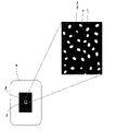
- FIG. FIG. 4 is a schematic diagram showing a state in which parallel laser beams reflected by the surface of a semiconductor die enter an imaging element of a camera when the semiconductor device is stationary and not subjected to ultrasonic vibration
- FIG. 3 is a schematic diagram showing an image captured by a camera in the state of FIG. 2
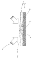
- FIG. 10 is a schematic diagram showing vibration of a bonding failure portion when a semiconductor device is subjected to ultrasonic vibration
- FIG. 4 is a schematic diagram showing vibration of a parallel laser beam reflected on the surface of a semiconductor die and a state in which the reflected laser beam enters an imaging element of a camera when a defective joint portion vibrates due to ultrasonic vibration of the semiconductor device.
- 6 is a schematic diagram showing an image captured by a camera in the state of FIG. 5;
- FIG. FIG. 2 is a schematic diagram showing pixels of an imaging element of a camera;
- FIG. 4 is a schematic diagram showing a visualized image displayed on a display; 2 is a flow chart showing the operation of the defect detection device shown in FIG. 1; 2 is a flow chart showing an operation of specifying a vibration-occurring pixel of the defect detection device shown in FIG.
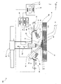
- FIG. 11 is a system diagram showing the configuration of a defect detection device according to another embodiment that ultrasonically vibrates a semiconductor device with an ultrasonic transducer;
- FIG. 10 is a diagram showing changes in impedance of an ultrasonic transducer and changes in current of high-frequency power with respect to the frequency of high-frequency power when the voltage of high-frequency power supplied to the ultrasonic transducer is constant in the prior art;
- FIG. 11 is a system diagram showing the configuration of a defect detection device according to another embodiment that ultrasonically vibrates a semiconductor device with an ultrasonic transducer
- FIG. 10 is a diagram showing changes in impedance of an ultrasonic transducer and changes in current of high-frequency power with respect to the frequency of high-frequency power when the voltage of high-frequency power supplied to the ultrasonic transducer is constant in the prior art;
- FIG. 13 is a flowchart showing the operation of the defect detection device shown in FIG. 12;
- FIG. 13 is a diagram showing a map that predefines changes in the voltage of high-frequency power with respect to the frequency of high-frequency power so that the current of high-frequency power supplied to the ultrasonic transducer is constant in the defect detection device of the embodiment shown in FIG. is.
- the defect detection device of the embodiment shown in FIG. 12 shows that the defect detection device of the embodiment shown in FIG.
- the change in the voltage of the high-frequency power with respect to the frequency of the high-frequency power is defined in advance so that the current of the high-frequency power supplied to the ultrasonic transducer is within a predetermined range.
- the defect detection apparatus 100 includes a stage 10 , an acoustic head 20 , a laser light source 30 , a camera 40 , a control section 50 and a detection section 55 .
- a direction perpendicular to the plane of FIG. 1 is defined as the X direction
- a horizontal direction perpendicular to the X direction is defined as the Y direction
- a vertical direction is defined as the Z direction.
- FIG. 1 shows five ultrasonic speakers 21 attached to the casing 22 of the acoustic head 20. When the ultrasonic speakers 21 are not distinguished, they are called the ultrasonic speakers 21. When distinguishing the ultrasonic speakers 21, they are referred to as ultrasonic speakers 211-215.
- the stage 10 is attached to a base (not shown).
- the stage 10 attracts and holds a semiconductor device 13, which is an inspection object, on an upper holding surface 10a.
- the semiconductor device 13 may be composed of, for example, a substrate 11 and a semiconductor die 12 attached to the substrate 11 with an adhesive, or may be a semiconductor die 12 mounted on the substrate 11 by flip-chip mounting. Alternatively, a plurality of semiconductor dies 12 may be laminated on the substrate 11 by direct bonding.
- the semiconductor device 13 has a semiconductor die 12 bonded onto a substrate 11 with an adhesive. (See Figure 4). Incidentally, in the following description, the portion above the gap 90 of the semiconductor die 12 is referred to as the defective portion 14 .
- An acoustic head 20 is arranged above the holding surface 10a side of the stage 10 so as to be spaced apart from the stage 10 .
- the acoustic head 20 is composed of a casing 22 and a plurality of ultrasonic speakers 21 attached to the casing 22 .
- a casing 22 of the acoustic head 20 is suspended by a rod 29a from a slider 29 attached to a guide rail 28 provided on the stage 10 so as to be movable in the Y direction.
- the casing 22 of the acoustic head 20 has a spherical dome shape and is open on the lower stage side.
- a spherical center 26 of a spherical surface forming casing 22 is positioned above surface 15 of semiconductor device 13 held on holding surface 10 a of stage 10 .
- the ultrasonic speaker 21 is an ultrasonic generator having directivity, and generates ultrasonic waves 24 so that the ultrasonic waves 24 propagate in the direction of the axis 21a within the range of the directivity angle ⁇ centered on the axis 21a.
- the frequency f of the ultrasonic wave 24 ranges from several tens of kHz to several hundreds of kHz.
- a plurality of ultrasonic speakers 21 are attached to the casing 22 so that each axis 21 a intersects at the spherical center 26 of the spherical surface of the casing 22 . Therefore, each ultrasonic wave 24 generated from the plurality of ultrasonic speakers 21 is concentrated on the surface 15 of the semiconductor device 13 held on the holding surface 10a where the spherical center 26 is located. A region where the ultrasonic waves 24 are concentrated is a detection region 27 for detecting defects. As shown in FIG. 1, the size of the detection area 27 is larger than the size of the semiconductor die 12, and the semiconductor die 12 and the substrate 11 are ultrasonically vibrated.
- the ultrasonic speaker 21 constitutes an ultrasonic vibrator.
- a drive unit 23 for driving the ultrasonic speaker 21 is connected to each ultrasonic speaker 21 .
- Each drive unit 23 supplies high-frequency power to each of the ultrasonic speakers 211-215 to drive each of the ultrasonic speakers 211-215. Further, each driving unit 23 is capable of adjusting each phase of each ultrasonic wave 24 generated by each connected ultrasonic speaker 211 to 215 respectively.
- the drive unit 23 that drives each ultrasonic speaker 21 is connected to the control section 50 and driven by commands from the control section 50 .
- the control unit 50 is a computer that includes a CPU 51 that is a processor that performs information processing and a storage unit 52 that stores control programs and control data.
- the laser light source 30 converts a single-wavelength laser beam output from a laser oscillator into a parallel laser beam 32 by a beam expander, and irradiates the semiconductor device 13 with the single-wavelength parallel laser beam 32 .
- the laser light source 30 is attached to the casing 22 of the acoustic head 20 so that the optical axis 31 is inclined with respect to the stage 10 and passes through the spherical center 26 . That is, the laser light source 30 is attached to the casing 22 so as to irradiate the detection area 27 on the surface 15 of the semiconductor device 13 with the parallel laser light 32 obliquely from above.
- the parallel laser beam 32 is highly coherent coherent light
- the laser light source 30 is a coherent light source that irradiates coherent light. Note that the laser light source 30 may not include a beam expander.
- the camera 40 includes an imaging device 42 composed of a plurality of pixels 46 (see FIG. 7), and captures a two-dimensional image of the semiconductor device 13 irradiated with the parallel laser light 32.
- camera 40 is mounted on casing 22 such that optical axis 41 is perpendicular to stage 10 and passes through sphere center 26 .
- camera 40 is attached to casing 22 so as to image detection area 27 on surface 15 of semiconductor device 13 from directly above.
- the camera 40 can be attached obliquely to the casing 22 rather than directly above the detection area 27 as long as the camera 40 can capture an image of the semiconductor device 13 irradiated with the parallel laser beam 32 from the laser light source 30 .
- the camera 40 may be one that captures a moving image or one that captures a still image.
- the laser light source 30 and the camera 40 are connected to the detection section 55.
- the detection unit 55 processes the two-dimensional image captured by the camera 40 to detect the defective area 91 (see FIG. 8).
- the detection unit 55 is a computer including a CPU 56 that is a processor that performs information processing, a storage unit 57 that stores control programs and control data, and a display 58 that displays the visualized image 12e (see FIG. 10). Also, the detection unit 55 is connected to the control unit 50 to exchange data.
- the surface 15 of the semiconductor die 12 bonded onto the substrate 11 has fine irregularities. Therefore, when the surface 15 of the semiconductor die 12 is irradiated with the parallel laser beam 32 while the semiconductor device 13 is not subjected to ultrasonic vibration, the parallel laser beam 32 is reflected in random directions from the surface 15 of the semiconductor die 12 .
- the reflected laser beams 33 reflected in random directions interfere with each other, and an interference pattern of the reflected laser beams 33 appears on the surface of the imaging device 42 of the camera 40 .
- the imaging element 42 of the camera 40 causes the interference pattern to appear on the surface of the image of the semiconductor die 12 as shown in FIG.
- An image 12a of a spotted pattern composed of a large number of bright portions 16 and dark portions 17 is obtained.
- the camera 40 acquires an image 12a of the semiconductor die 12 with a speckled pattern, as shown in the field of view 43 of FIG.
- the image 12a is an image containing the interference pattern when the semiconductor die 12 is stationary.
- the camera 40 acquires an interference pattern image 14a of the defective portion 14 that is the same as that of other portions.
- each ultrasonic speaker 21 is driven by each drive unit 23 to generate an ultrasonic wave 24 with a predetermined frequency f from each ultrasonic speaker 21 .
- Ultrasonic waves 24 generated from each ultrasonic speaker 21 intersect in a detection area 27 in the vicinity of the spherical center 26 of the casing 22, are concentrated and overlapped, and pass through the semiconductor device 13 composed of the substrate 11 and the semiconductor die 12. Apply sonic vibration.
- the surface 15 of the semiconductor die 12 vibrates as indicated by an arrow 96 shown in FIG.
- the optical path of the reflected laser beam 33 is shifted as indicated by an arrow 97 between the optical path 34a and the optical path 34b shown in FIG. This optical path blurring occurs at the same vibration period as the ultrasonic vibration of the semiconductor die 12 .
- the image 14a of the defective portion 14 of the semiconductor die 12 having the speckled pattern on the imaging device 42 described with reference to FIG. 14b Due to the blurring of the optical paths 34a and 34b, the image 14a of the defective portion 14 of the semiconductor die 12 having the speckled pattern on the imaging device 42 described with reference to FIG. 14b.
- the camera 40 captures an image of the interference pattern of the defective portion 14 as shown in FIG.
- An image 14b of blurred speckled pattern is obtained.
- portions of the semiconductor die 12 that are well bonded to the substrate 11 other than the defective portion 14 hardly vibrate with respect to the substrate 11 . Therefore, the image 12a other than the defective portion 14 of the semiconductor die 12 having the speckled pattern on the imaging element 42 is not blurred. Therefore, the camera 40 acquires the image 12a of the speckled pattern without blurring as described with reference to FIG.
- the intensity of the brightness of the pixels 46 of the imaging device 42 is lower than the brightness of the interference pattern image 14a in a static state without ultrasonic vibration or in a non-vibrating state. Varies relative to intensity.
- the intensity of the brightness of the pixel 46 is greater than that of the interference pattern image 14a in the non-vibrating state.
- the interference pattern image 12a is the interference pattern image 12a when the semiconductor die 12 is in a stationary state or in a non-vibrating state. It does not blur like the image 12a. Therefore, in portions other than the defective portion 14, the intensity of brightness of the pixels 46 of the imaging device 42 is substantially the same as the intensity of brightness when the semiconductor die 12 is in a stationary state without ultrasonic vibration or in a non-vibrating state. .
- the detection unit 55 detects pixels 46 in which the intensity of brightness during ultrasonic vibration changes from the intensity of brightness during rest or non-vibration without ultrasonic vibration. Vibration generation pixels 47 are identified, and a region including the identified vibration generation pixels 47 is detected as a defective region 91 as shown in FIG.
- the detection unit 55 displays on the display 58 a visualized image 12e in which the image of the semiconductor die 12 includes the display 18 corresponding to the specified vibration generation pixels 47, as shown in FIG.
- the presence or absence of the defective portion 14 can be determined from the display on the display 58 .
- step S101 of FIG. 9 the CPU 56 of the detection unit 55 outputs an irradiation command of the parallel laser beam 32 to the laser light source 30.
- the laser light source 30 irradiates the semiconductor die 12 of the semiconductor device 13 with the parallel laser light 32 .
- the CPU 56 of the detection unit 55 proceeds to step S102 in FIG. 9, and as shown in FIGS. Images 12a and 14a including interference patterns generated by interference of light 33 are acquired (still image acquisition step).
- the CPU 56 proceeds to step S103 in FIG. 9 and stores the images 12a and 14a including the acquired interference patterns in the storage unit 57.
- the CPU 56 of the detection unit 55 advances to step S104 in FIG. 9 and outputs a signal to start driving the ultrasonic speaker 21 to the control unit 50 .
- the CPU 51 of the control section 50 outputs a command to each drive unit 23 to start driving the ultrasonic speaker 21 .
- Each drive unit 23 drives the ultrasonic speaker 21 according to this command to generate an ultrasonic wave 24 having a predetermined frequency f from each ultrasonic speaker 21 .
- Each ultrasonic speaker 21 has directivity, and propagates in the direction of each axis 21a within a range of a directivity angle ⁇ centered on the axis 21a.
- Each ultrasonic speaker 21 is attached to the casing 22 so that each axis 21 a intersects at the spherical center 26 of the casing 22 . intersects in the vicinity of , and is centrally superimposed.
- the CPU 51 of the control unit 50 adjusts each phase of each ultrasonic speaker 21 by each drive unit 23 so that the amplitude of ultrasonic vibration increases in the vicinity of the sphere center 26 by superimposing the ultrasonic waves 24 .
- the phases of the ultrasonic waves 24 generated by the ultrasonic speakers 211 and 215 located symmetrically with respect to the spherical center 26 are shifted by 180 degrees.
- the CPU 51 may adjust the phases of the ultrasonic waves 24 generated by the ultrasonic speakers 211 to 215 by the driving unit 23 so as to disperse them. This makes it possible to increase the amplitude of ultrasonic vibration in the detection area 27, which is the range in which the ultrasonic waves 24 near the sphere center 26 are concentrated.
- the CPU 51 of the control unit 50 causes the ultrasonic speaker 21 to generate ultrasonic waves 24 by the drive unit 23 to ultrasonically vibrate the semiconductor device 13 composed of the substrate 11 and the semiconductor die 12 .
- the defective portion 14 having the defective gap 90 between the substrate 11 and the semiconductor die 12 is formed by the semiconductor die 12 as indicated by an arrow 95 in FIG. It vibrates greatly with respect to the substrate 11 .
- the CPU 51 of the control section 50 When the ultrasonic excitation by the ultrasonic speaker 21 is started, the CPU 51 of the control section 50 outputs to the detection section 55 a signal during ultrasonic excitation and the frequency f of the ultrasonic excitation. When this signal is input, the CPU 56 of the detection unit 55 sets the exposure time of the camera 40 longer than the period of the ultrasonic vibration in step S105 of FIG. An image 12a, 14b containing the interference pattern at the time is acquired.
- the camera 40 captures the image of the interference pattern of the defective portion 14 as a blur as shown in FIG.
- An image 14b of a spotted pattern is acquired.
- the image 12a of the speckled pattern without blurring as described with reference to FIG. 3 is acquired (image acquisition step during ultrasonic vibration).
- the CPU 56 of the detection unit 55 proceeds to step S106 in FIG.
- step S107 of FIG. 9 the CPU 56 of the detection unit 55 reads out the images 12a and 14a including the interference pattern when the semiconductor die 12 is stationary and the images 12a and 14b including the interference pattern when the semiconductor die 12 is vibrating ultrasonically from the storage unit 57.
- Steps S201 to S201 of FIG. 10 are executed, and the vibration generation pixel 47 is detected based on the deviation between the images 12a and 14a including the interference pattern at rest and the images 12a and 14b including the interference pattern at the time of ultrasonic vibration. Identify.
- FIG. 7 Details of the specific operation of the vibration generating pixel 47 will be described below with reference to FIGS. 7 and 10.
- FIG. The CPU 56 of the detection unit 55 regards the pixels 46 in which the intensity of brightness during ultrasonic vibration changes from the intensity of brightness at rest without ultrasonic vibration or during non-vibration as vibration generation pixels 47 . Identify.
- the CPU 56 of the detection unit 55 performs the processing described below on each pixel 46 of the image frame 45, which is one region of the two-dimensional image of the field of view 43 to be subjected to image processing at once, and vibrates.
- the generation pixel 47 is specified.
- the coordinates (x,y) that follow the reference numerals refer to the coordinates (x,y) of the two-dimensional image frame 45, e.g. , a pixel 46 is shown.
- the CPU 56 of the detection unit 55 extracts an ultrasonic image from the two-dimensional image obtained from the camera 40 stored in the storage unit 57 and the two-dimensional image at rest or without vibration.
- An image frame 45v at the time of sound wave vibration and an image frame 45s at the time of rest are read.
- the CPU 56 determines the deviation between the brightness intensity Iv (x, y) during ultrasonic vibration and the average value Ia (x, y) at each pixel 46 (x, y).
- the average value in the image frame 45 of the absolute values is calculated as the average absolute deviation value.
- Mean absolute deviation Average value of
- the CPU 56 calculates the normalized pixel intensity squared value NIave(x, y) by the following (Equation 1).
- NI ave (x, y) [
- step S205 of FIG. 10 when NIave(x, y) is 1 or more, the CPU 56 determines that the change in brightness intensity of the pixel 46 (x, y) is significant. 10, the pixel 46 (x, y) is specified as the vibration generation pixel 47 (x, y), and the process proceeds to step S207.
- the CPU 56 determines in step S207 that all pixels 46 (x, y) of the image frame 45 have not been processed, the process returns to step S204 to process the next pixel 46 (x, y).
- the CPU 56 determines NO in step S205 of FIG. 10
- the process returns to step S204 to process the next pixel 46 (x, y).
- the CPU 56 calculates NIave (x, y) for all pixels 46 (x, y) of the image frame 45, and after specifying the vibration-occurring pixel 47 (x, y) in the image frame 45, the step of FIG. YES is determined in S207, and the process proceeds to step S208 in FIG.
- step S208 of FIG. 10 the CPU 56 confirms whether a predetermined number of other vibration-generated pixels 47 (x1, y1) exist within a predetermined range around one vibration-generated pixel 47 (x, y). For example, a square array 48 of 5 ⁇ 5 pixels 46 centered on the vibration generating pixel 47 (x, y) is set as the predetermined range, and 7 to 8 other vibration generating pixels 47 (x1 , y1) exists. If it is determined YES in step S208 of FIG. 10, it is determined that the change in brightness intensity of the pixel 46 (x, y) is caused by ultrasonic vibration, and the process proceeds to step S209 of FIG. maintains the identification of the pixel 46 (x, y) as the vibration generating pixel 47 (x, y).
- the CPU 56 determines the identification of the vibration generation pixel 47 (x, y).
- the CPU 56 performs the above processing for each image frame 45 and determines the identification of the vibration generation pixels 47 (x, y) for all the pixels 46 (x, y) of the image sensor 42 .
- step S108 the CPU 56 of the detection unit 55 proceeds to step S108 in FIG.
- a defective area 91 is set to an area in which the vibration generation pixels 47 specified in step S107 are densely packed to a predetermined value or more.
- the array 48 may be set as the vibration generating array, and the area where the vibration generating arrays are continuous may be set as the defective area 91 .
- a region in which the length or area of continuous vibration generating arrays is equal to or greater than a predetermined threshold value is set as a defective region 91, and when the length or area of continuous vibration generating arrays is less than a predetermined threshold value, It may not be set as the defective area 91 .
- the predetermined threshold value may be set by a comparison test between non-defective products and non-defective products. For example, in the case of a non-defective semiconductor die 12 having continuous vibration generating arrays of about 0.05 mm, the predetermined threshold value may be set to, for example, 0.08 mm to 0.1 mm.
- the predetermined threshold may be changed depending on the region where the vibration generating array is continuous. For example, in the semiconductor device 13 in which a plurality of semiconductor dies 12 are directly bonded, the predetermined threshold is may be set smaller than other portions to strictly check the connection between the electrodes. Further, the predetermined threshold value may be decreased in the periphery of the semiconductor die 12 and increased in the center. Conversely, the predetermined threshold value may be increased in the periphery of the semiconductor die 12 and increased in the center. You can set it smaller.
- the defective region 91 may be set by image analysis of the distribution image of the vibration-generating pixels 47 in the semiconductor device 13 and the distribution image of the vibration-generating pixels 47 in the semiconductor device 13 to be inspected.
- step S109 in FIG. 9 determines whether the setting of the defective area 91 has been completed.
- the CPU 56 of the detection unit 55 determines YES in step S109 of FIG. 9, it outputs a defect detection signal to the outside in step S110 of FIG. At this time, information on the position and shape of the defective area 91 may be output together.
- the CPU 56 of the detection unit 55 determines that no defect is detected, and determines that the semiconductor device 13 to be inspected is a non-defective product in step S111 of FIG. Outputs a non-defective product detection signal.
- Display step> As shown in FIG. 8, the CPU 56 of the detection unit 55 displays on the display 58 a visualized image 12e in which the image of the semiconductor die 12 includes the display 18 corresponding to the specified vibration generation pixel 47 in step S112 of FIG. (display step).
- the visualized image 12e can be of various formats, but in FIG. 8, as an example, vibration-generated pixels 47 of a general image of the semiconductor die 12 obtained by irradiating the semiconductor die 12 with non-interfering light rays such as electric lights are shown. A red dot is superimposed as a display 18 on the portion corresponding to . According to this image, red dots, which are many indications 18, are displayed in the area near the defective portion 14 that is vibrating due to ultrasonic vibration, and indications 18 are displayed in portions other than the defective portion 14 that is not vibrating. , the red dot is almost invisible. In the example shown in FIG.
- the CPU 56 of the detection unit 55 may display the defective area 91 set in step S108 of FIG. 9 so as to be superimposed on the visualized image 12e.
- the defective area 91 and the display 18 are superimposed on the general image of the semiconductor die 12, and it is possible to visually confirm whether or not a defect has been detected.
- the defect detection apparatus 100 irradiates the semiconductor device 13 with the parallel laser beam 32 to perform ultrasonic vibration, and obtains images 12a and 14a including the interference pattern at rest and images 12a and 14a at the time of ultrasonic vibration. Since the defect is detected based on the deviation from the images 12a and 14b including the interference patterns of , the defect of the semiconductor device 13 can be detected in a short time with a simple configuration.
- the defect detection apparatus 100 detects the pixel 46 (x , y) are attributed to ultrasonic vibrations, and the identification of pixel 46 (x, y) as vibration generating pixel 47 (x, y) is maintained, otherwise Then, the identification as the vibration generation pixel 47 (x, y) is cancelled. As a result, it is possible to prevent the pixels 46 that are not actually vibrating due to noise from being identified as the vibration-occurring pixels 47, and to detect vibrations and defects with high accuracy.
- the defect detection apparatus 100 detects defects by setting an area in which the specified vibration-generating pixels 47 are densely packed with a predetermined value or more as the defect area 91.
- a defect can be detected based on the deviation from the images 12a and 14b including the interference pattern during ultrasonic excitation.
- the defect detection device 100 displays the visualized image 12e of the defective portion 14 on the display 58, it is possible to easily determine the presence or absence of a defect simply by visually recognizing the display 58.
- the defect detection apparatus 100 of the embodiment indirectly ultrasonically vibrates the semiconductor device 13 by concentrating the ultrasonic waves 24 on the semiconductor device 13 using the acoustic head 20 having a plurality of ultrasonic speakers 21 attached thereto. Since the defect is detected, the defect can be detected with a simple structure. In addition, since the semiconductor device 13 is indirectly subjected to ultrasonic vibration, it is possible to detect defects in the semiconductor device 13 without contact.
- the laser light source 30 irradiates the semiconductor device 13 with the parallel laser beam 32 of a single wavelength. It is also possible to irradiate laser light that does not exist. Also, the laser light may have some unevenness in intensity.
- the images 12a, 14a, and 14b of the interference pattern are spotted patterns including a large number of bright portions 16 and dark portions 17, but are not limited to this, and may be other patterns such as striped patterns. may
- a plurality of laser light sources 30 and cameras 40 are prepared to irradiate the semiconductor device 13 with laser light from multiple directions, and the plurality of cameras 40 are used to irradiate the semiconductor device 13 in multiple directions. It is also possible to detect defects by detecting vibrations in multiple directions by picking up images from the .
- the semiconductor device 13 is described as an object to be inspected, but the present invention may be applied to the detection of bonding defects between layers of other products in which plate members are stacked and bonded.
- Examples of other products obtained by laminating and joining plate-like members include laminated plates and laminate materials.
- the defect detection apparatus 200 of the embodiment is an acoustic head in which the acoustic head 20 of the defect detection apparatus 100 described with reference to FIG. 60.
- the casing 62 is an annular member having a small diameter open surface 64 on the upper side and an open surface 65 with a large diameter on the lower side. ing.
- a spherical center 66 of the spherical surface 63 is positioned above the surface 15 of the semiconductor device 13 held on the holding surface 10 a of the stage 10 .
- a plurality of ultrasonic speakers 21 are attached to the casing 62 so that the respective axes 21 a intersect at the spherical center 66 of the spherical surface of the casing 62 . Similar to the defect detection apparatus 100 described above with reference to FIG. 1, the ultrasonic waves 24 generated from the respective ultrasonic speakers 21 intersect at the sphere center 66 and are concentrated and superimposed. By superimposing the ultrasonic waves 24, a detection area 27 having a large amplitude of ultrasonic vibration is formed in the vicinity of the spherical center 66.
- the operation of the defect detection device 200 is the same as the operation of the defect detection device 100 previously described with reference to FIG.
- the casing 62 of the defect detection device 200 is composed of a ball base-shaped annular member, the thickness in the Z direction can be reduced, and it can be incorporated into a compact bonding device or the like.
- FIG. 12 The defect detection device 300 ultrasonically excites the semiconductor device 13 by an ultrasonic vibrator 70 connected to the semiconductor device 13 instead of the acoustic head 20 of the defect detection device 100 described with reference to FIG. .
- the ultrasonic transducer 70 constitutes an ultrasonic exciter.
- the configurations of the laser light source 30, the camera 40, and the detection unit 55 are the same as those of the defect detection apparatus 100 described above.
- the ultrasonic transducer 70 is driven by a drive unit 23 that supplies high-frequency power to the ultrasonic transducer 70 .
- the ultrasonic transducer 70 may be composed of, for example, a piezo element or the like. Between the drive unit 23 and the ultrasonic transducer 70 are a voltage sensor 53 that detects the voltage of the high frequency power supplied from the drive unit 23 to the ultrasonic transducer 70, and a current sensor 54 that detects the current of the high frequency power. and are installed.
- the voltage sensor 53 and current sensor 54 are connected to the control unit 50 , and voltage and current data of the high-frequency power detected by the voltage sensor 53 and current sensor 54 are input to the control unit 50 .
- the control unit 50 captures an image of the semiconductor device 13 with the camera 40 while changing the frequency of the high-frequency power supplied from the drive unit 23 to the ultrasonic transducer 70, and determines the defect of the semiconductor device 13 based on the captured image. detect.
- the ultrasonic transducer 70 itself resonates at frequency f1.
- the impedance of the ultrasonic transducer 70 is greatly reduced at the frequency f1 as indicated by the dashed line a in FIG.
- the impedance of ultrasonic transducer 70 rises significantly.
- both the substrate 11 and the semiconductor die 12 vibrate greatly at the frequency f1 at which the ultrasonic oscillator 70 resonates. Can be hidden and difficult to detect.
- the vibrations of the substrate 11 and the semiconductor die 12 are so small that the vibration of the defective portion 14 of the semiconductor die 12 may not be detected.
- the frequency f1 at which the ultrasonic transducer 70 resonates In some cases, the detection of the defective portion 14 of the semiconductor die 12 becomes difficult.
- the defect detection apparatus 300 of the embodiment focusing on the fact that the amplitude of the ultrasonic transducer 70 is proportional to the current of the high-frequency power input to the ultrasonic transducer 70, the high-frequency power input to the ultrasonic transducer 70
- the current A1 of the power is detected by the current sensor 54, and the voltage V1 of the high-frequency power is adjusted so that the detected current A1 is within a predetermined range.
- the current A1 of the high-frequency power can be kept within a predetermined range, and the amplitude of the ultrasonic transducer 70 can be kept within a predetermined range.
- the current A1 detected by the current sensor 54 is fed back to the control unit 50, and in the vicinity of the frequency f1 where the current A1 of high-frequency power increases, as indicated by the dashed-dotted line c1 in FIG.
- the voltage V1 of the high-frequency power supplied to the sound wave oscillator 70 is lowered.
- the voltage V1 of the high-frequency power supplied to the ultrasonic transducer 70 is increased as indicated by the dashed-dotted line c1 in FIG.
- the magnitude of the current A1 detected by the current sensor 54 can be kept substantially constant regardless of the frequency f.
- the vibration of the substrate 11 and the semiconductor die 12 can be made substantially constant by making the amplitude of the element 70 substantially constant.
- the substrate 11 and the semiconductor die 12 are greatly vibrated at a specific frequency, and the vibration of the substrate 11 and the semiconductor die 12 hides defects. It is possible to prevent the vibration of the portion 14 from being undetectable.
- the detection unit 55 irradiates the semiconductor device 13 with the parallel laser beam 32 to acquire images 12a and 14a of the interference pattern at rest and store them in the storage unit 57.
- the detection unit 55 After storing the stationary interference pattern images 12 a and 14 a in the storage unit 57 , the detection unit 55 outputs a signal to start driving the ultrasonic transducer 70 to the control unit 50 .
- the CPU 51 of the control section 50 When this signal is input, the CPU 51 of the control section 50 outputs a command to start driving the ultrasonic transducer 70 to the driving unit 23 as in step S304 of FIG.
- the drive unit 23 drives the ultrasonic vibrator 70 according to this command to ultrasonically vibrate the semiconductor device 13 .
- the CPU 51 of the control unit 50 adjusts the voltage V1 of the high-frequency power so that the current A1 detected by the current sensor 54 is substantially constant, as in step S304 of FIG.
- the semiconductor device 13 is ultrasonically vibrated by the ultrasonic transducer 70 while changing the frequency f to f3 (f0 ⁇ f3).
- the CPU 51 of the control unit 50 When the ultrasonic vibration of the semiconductor device 13 is started by the ultrasonic transducer 70, the CPU 51 of the control unit 50 outputs to the detection unit 55 a signal during ultrasonic vibration and the start frequency f0 of ultrasonic vibration. When this signal is input, the CPU 56 of the detection unit 55 sets the exposure time of the camera 40 to be longer than the cycle of the start frequency f0 of the ultrasonic vibration in step S105 of FIG. Images 12a and 14b including the interference pattern at the time of ultrasonic vibration described above are obtained, and the images 14a and 14b are stored in the storage unit 57 in step S106 of FIG. The camera 40 may pick up the images 12a, 14a, and 14b as moving images and store the moving image data in the storage unit 57.
- the image may be captured as a still image.
- 12a, 14a, and 14b may be captured and data sets of a plurality of still images may be stored in the storage unit 57.
- the CPU 56 of the detection unit 55 identifies the vibration-occurring pixels 47 in step S107 of FIG. 15 in the same manner as in the defect detection apparatus 100 described above, and determines in step S108 of FIG. A defective area 91 is set as the area where the defect is present. If YES is determined in step S109 of FIG. 15, a defect detection signal is output in step S110 of FIG. 15, and if NO is determined in step S109 of FIG. Output a signal. Then, the visualized image 12e is displayed on the display 58 in step S112 of FIG.
- the defect detection apparatus 300 sets the amplitude of the ultrasonic transducer 70 within a predetermined range when the semiconductor device 13 is ultrasonically excited by changing the frequency of the high-frequency power. It is possible to suppress the substrate 11 and the semiconductor die 12 from greatly vibrating at the frequency of . As a result, it is possible to prevent the vibration of the defective portion 14 from being hidden by the vibration of the substrate 11 and the semiconductor die 12 at a specific frequency, and the detection accuracy of the defective portion 14 can be improved.
- the defect detection apparatus 300 ultrasonically excites the semiconductor device 13, and produces images 12a and 14a including interference patterns at rest and images 12a and 14a including interference patterns at the time of ultrasonic excitation. Since the defect is detected based on the deviation from 14b, the defect of the semiconductor device 13 can be detected in a short time with a simple configuration.
- the change in the current A0 of the high-frequency power when the frequency is changed while the voltage V0 of the high-frequency power is kept constant is obtained by a test or the like. , and stores this voltage waveform in the storage unit 52 as a map 59a showing changes in the voltage V2 with respect to the frequency f.
- the map 59a has a waveform in which the voltage decreases near the frequency f1 and increases near the frequency f2. Then, when performing ultrasonic excitation, the voltage corresponding to the frequency f may be adjusted by referring to the map 59a stored in the storage unit 52.
- FIG. Also in this case, as indicated by the solid line d2 in FIG. 16, the current A2 supplied to the ultrasonic transducer 70 is substantially constant even if the frequency changes.
- the semiconductor device 13 when the semiconductor device 13 is subjected to ultrasonic vibration in various frequency bands with a simple configuration, the entire semiconductor device 13 vibrates greatly, and the vibration of the defective portion 14 is hidden behind the vibration of the substrate 11 and the semiconductor die 12. Impossibility of detection can be suppressed, and a defect of the semiconductor device 13 can be detected with high accuracy.
- a voltage waveform that causes the voltage V3 to change stepwise with respect to the frequency f is stored as a map 59b in the storage unit 52.
- the current A3 supplied to the ultrasonic transducer 70 does not become substantially constant, but falls within a predetermined range ⁇ A.
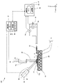
- a defect detection device 400 of another embodiment will be described with reference to FIG. 12 to 17, between each drive unit 23 and each ultrasonic speaker 21 (ultrasonic speakers 212 to 215) of the defect detection device 100 described with reference to FIG. Similar to the failure detection device 300 described above, a voltage sensor 53 and a current sensor 54 are attached. 18 shows only one ultrasonic speaker 211 attached to the acoustic head 20, and the other ultrasonic speakers 212 to 215 are omitted. Also, only the vicinity of the ultrasonic speaker 211 of the casing 22 is shown, and other parts are omitted.
- the operation of the defect detection apparatus 400 is the same as that of the defect detection apparatus 300, except that the ultrasonic transducers 70 are driven by the drive unit 23, and the respective ultrasonic speakers 21 are driven by the plurality of drive units 23. is similar to the behavior of
- the defect detection device 400 performs feedback control so that the current A1 of the high frequency power supplied from each drive unit 23 to each ultrasonic speaker 21 is substantially constant, so that even when the frequency f of the high frequency power is changed,
- the ultrasonic vibration force applied to the semiconductor device 13 by each ultrasonic speaker 21 can be substantially constant, and the vibration of the substrate 11 and the semiconductor die 12 can be substantially constant.
- the defect detection apparatus 300 when the semiconductor device 13 is subjected to ultrasonic vibration by changing the frequency of the high-frequency power, the substrate 11 and the semiconductor die 12 are greatly vibrated at a specific frequency. It is possible to prevent the vibration of the defective portion 14 from being hidden by the vibration of the defective portion 12 and becoming undetectable.
- the defect detection apparatus 400 ultrasonically excites the semiconductor device 13, and produces images 12a and 14a including the interference pattern at rest and images 12a and 14a including the interference pattern at the time of ultrasonic excitation. Since the defect is detected based on the deviation from 14b, the defect of the semiconductor device 13 can be detected in a short time with a simple configuration. In addition, since the semiconductor device 13 is indirectly subjected to ultrasonic vibration, it is possible to detect defects in the semiconductor device 13 without contact.
- the defect detection apparatuses 100, 200, 300, and 400 described above all set the defect area 91 and detect defects in the semiconductor device 13, which is the object to be inspected.
- it functions as a vibration detection device that identifies the vibration location of the semiconductor device 13, which is the inspection object, by displaying the vibration generation pixel indicating the vibration generation location on the display 58. You may let
- the detection unit 55 processes the image captured by the camera 40 to identify the vibration generation pixel 47 indicating the vibration generation location, and the identified pixel 47 is added to the image of the semiconductor device 13 A visualized image 12 e including a display corresponding to the vibration generation pixels 47 is displayed on the display 58 .
- the defect detection device 100 When the defect detection device 100 is caused to function as a vibration detection device, the presence or absence of a defect is judged by an inspector by viewing the image on the display 58 .
- Such an operation is useful, for example, when the semiconductor device 13 is new and there is no threshold or predetermined value for setting the defective area 91 .
Landscapes
- Physics & Mathematics (AREA)
- General Physics & Mathematics (AREA)
- Pathology (AREA)
- Life Sciences & Earth Sciences (AREA)
- Chemical & Material Sciences (AREA)
- Analytical Chemistry (AREA)
- Biochemistry (AREA)
- General Health & Medical Sciences (AREA)
- Health & Medical Sciences (AREA)
- Immunology (AREA)
- Acoustics & Sound (AREA)
- Optics & Photonics (AREA)
- Engineering & Computer Science (AREA)
- Computer Vision & Pattern Recognition (AREA)
- Signal Processing (AREA)
- Investigating Or Analyzing Materials By The Use Of Ultrasonic Waves (AREA)
- Investigating Materials By The Use Of Optical Means Adapted For Particular Applications (AREA)
- Testing Or Measuring Of Semiconductors Or The Like (AREA)
- Measurement Of Mechanical Vibrations Or Ultrasonic Waves (AREA)
Priority Applications (6)
| Application Number | Priority Date | Filing Date | Title |
|---|---|---|---|
| CN202180044011.8A CN115769071B (zh) | 2021-01-21 | 2021-01-21 | 不良检测装置以及不良检测方法 |
| KR1020237009698A KR102811974B1 (ko) | 2021-01-21 | 2021-01-21 | 불량 검출 장치 및 불량 검출 방법 |
| US18/273,548 US12487206B2 (en) | 2021-01-21 | 2021-01-21 | Defect detection device and defect detection method |
| PCT/JP2021/001929 WO2022157870A1 (ja) | 2021-01-21 | 2021-01-21 | 不良検出装置及び不良検出方法 |
| JP2022576284A JP7373874B2 (ja) | 2021-01-21 | 2021-01-21 | 不良検出装置及び不良検出方法 |
| TW111102297A TWI820581B (zh) | 2021-01-21 | 2022-01-20 | 不良檢測裝置、不良檢測方法以及振動檢測裝置 |
Applications Claiming Priority (1)
| Application Number | Priority Date | Filing Date | Title |
|---|---|---|---|
| PCT/JP2021/001929 WO2022157870A1 (ja) | 2021-01-21 | 2021-01-21 | 不良検出装置及び不良検出方法 |
Publications (1)
| Publication Number | Publication Date |
|---|---|
| WO2022157870A1 true WO2022157870A1 (ja) | 2022-07-28 |
Family
ID=82548591
Family Applications (1)
| Application Number | Title | Priority Date | Filing Date |
|---|---|---|---|
| PCT/JP2021/001929 Ceased WO2022157870A1 (ja) | 2021-01-21 | 2021-01-21 | 不良検出装置及び不良検出方法 |
Country Status (6)
| Country | Link |
|---|---|
| US (1) | US12487206B2 (https=) |
| JP (1) | JP7373874B2 (https=) |
| KR (1) | KR102811974B1 (https=) |
| CN (1) | CN115769071B (https=) |
| TW (1) | TWI820581B (https=) |
| WO (1) | WO2022157870A1 (https=) |
Cited By (1)
| Publication number | Priority date | Publication date | Assignee | Title |
|---|---|---|---|---|
| WO2025144103A1 (en) * | 2023-12-27 | 2025-07-03 | Semiconductor Technologies & Instruments Pte Ltd | System and method for inspecting devices for internal defects at about sidewalls thereof caused by wafer singulation processes |
Families Citing this family (3)
| Publication number | Priority date | Publication date | Assignee | Title |
|---|---|---|---|---|
| TWI847338B (zh) * | 2022-11-01 | 2024-07-01 | 華碩電腦股份有限公司 | 電子裝置之震動控制方法 |
| TWI874280B (zh) * | 2024-09-20 | 2025-02-21 | 新加坡商先進科技新加坡有限公司 | 用於電子器件的缺陷檢驗方法和裝置 |
| CN120495217B (zh) * | 2025-05-06 | 2026-01-23 | 徐州远翔机车科技有限公司 | 一种钢轮表面划痕检测方法及系统 |
Citations (12)
| Publication number | Priority date | Publication date | Assignee | Title |
|---|---|---|---|---|
| JPS6085363A (ja) * | 1983-10-17 | 1985-05-14 | Hitachi Ltd | 接合状態検出方法及びその装置 |
| JPS627200A (ja) * | 1985-07-03 | 1987-01-14 | 株式会社日立製作所 | 接合状態検出装置 |
| US5146289A (en) * | 1990-12-21 | 1992-09-08 | Laser Technology, Inc. | Nondestructive testing using air-coupled acoustic excitation |
| JPH07218449A (ja) * | 1994-02-04 | 1995-08-18 | Toyota Motor Corp | 光学的表面欠陥検出方法 |
| JP2004101189A (ja) * | 2002-09-04 | 2004-04-02 | Hitachi Ltd | 欠陥検査装置及び欠陥検査方法 |
| JP2007024674A (ja) * | 2005-07-15 | 2007-02-01 | Hitachi Ltd | 表面・表層検査装置、及び表面・表層検査方法 |
| JP2011058879A (ja) * | 2009-09-08 | 2011-03-24 | Mitsubishi Electric Corp | クラック検知支援装置 |
| JP2016130683A (ja) * | 2015-01-14 | 2016-07-21 | 東芝テック株式会社 | 振動計測装置 |
| JP2018132481A (ja) * | 2017-02-17 | 2018-08-23 | 学校法人桐蔭学園 | 解析装置及び解析システム |
| CN108613979A (zh) * | 2018-03-12 | 2018-10-02 | 华中科技大学鄂州工业技术研究院 | 用于粘弹性定量检测的激光散斑图像处理装置及方法 |
| DE102018221795A1 (de) * | 2018-12-14 | 2020-06-18 | Volkswagen Aktiengesellschaft | Vorrichtung zur Erzeugung eines haptisch wahrnehmbaren Bereiches sowie Konfigurations- und Steuerverfahren einer solchen Vorrichtung |
| CN111316093A (zh) * | 2018-12-14 | 2020-06-19 | 合刃科技(深圳)有限公司 | 结构缺陷检测系统及结构缺陷检测方法 |
Family Cites Families (14)
| Publication number | Priority date | Publication date | Assignee | Title |
|---|---|---|---|---|
| JPS61254834A (ja) | 1985-05-08 | 1986-11-12 | Matsushita Electric Ind Co Ltd | 走査型光音響顕微鏡装置 |
| JPH01145566A (ja) * | 1987-12-02 | 1989-06-07 | Shinkuraito:Kk | ボンディング状態検査装置 |
| JP5421763B2 (ja) * | 2009-12-24 | 2014-02-19 | ヤマハ発動機株式会社 | 検査装置および検査方法 |
| JP2014228486A (ja) * | 2013-05-24 | 2014-12-08 | インスペック株式会社 | 三次元プロファイル取得装置、パターン検査装置及び三次元プロファイル取得方法 |
| JP6433268B2 (ja) * | 2014-03-31 | 2018-12-05 | 国立大学法人 東京大学 | 検査システムおよび検査方法 |
| JP2016191552A (ja) | 2015-03-30 | 2016-11-10 | 三菱重工業株式会社 | 非破壊検査装置及び非破壊検査方法 |
| CN107710114A (zh) * | 2015-06-25 | 2018-02-16 | 富士通株式会社 | 电子设备、以及驱动控制方法 |
| CN206892031U (zh) * | 2016-07-12 | 2018-01-16 | 纳路易爱姆斯株式会社 | 具备位置识别飞行单元与图像拍摄部的检查用飞行体 |
| KR20190108598A (ko) * | 2017-03-29 | 2019-09-24 | 닛폰세이테츠 가부시키가이샤 | 결함 검출 장치, 결함 검출 방법 및 프로그램 |
| US10778912B2 (en) * | 2018-03-31 | 2020-09-15 | Open Water Internet Inc. | System and device for optical transformation |
| EP3779378B1 (en) * | 2018-04-05 | 2022-05-11 | Shimadzu Corporation | Vibration measurement device |
| WO2019239618A1 (ja) * | 2018-06-11 | 2019-12-19 | 株式会社島津製作所 | 欠陥検出方法及び装置 |
| US10966612B2 (en) * | 2018-06-14 | 2021-04-06 | Open Water Internet Inc. | Expanding beam optical element |
| US10962929B2 (en) * | 2018-09-14 | 2021-03-30 | Open Water Internet Inc. | Interference optics for optical imaging device |
-
2021
- 2021-01-21 JP JP2022576284A patent/JP7373874B2/ja active Active
- 2021-01-21 WO PCT/JP2021/001929 patent/WO2022157870A1/ja not_active Ceased
- 2021-01-21 CN CN202180044011.8A patent/CN115769071B/zh active Active
- 2021-01-21 US US18/273,548 patent/US12487206B2/en active Active
- 2021-01-21 KR KR1020237009698A patent/KR102811974B1/ko active Active
-
2022
- 2022-01-20 TW TW111102297A patent/TWI820581B/zh active
Patent Citations (12)
| Publication number | Priority date | Publication date | Assignee | Title |
|---|---|---|---|---|
| JPS6085363A (ja) * | 1983-10-17 | 1985-05-14 | Hitachi Ltd | 接合状態検出方法及びその装置 |
| JPS627200A (ja) * | 1985-07-03 | 1987-01-14 | 株式会社日立製作所 | 接合状態検出装置 |
| US5146289A (en) * | 1990-12-21 | 1992-09-08 | Laser Technology, Inc. | Nondestructive testing using air-coupled acoustic excitation |
| JPH07218449A (ja) * | 1994-02-04 | 1995-08-18 | Toyota Motor Corp | 光学的表面欠陥検出方法 |
| JP2004101189A (ja) * | 2002-09-04 | 2004-04-02 | Hitachi Ltd | 欠陥検査装置及び欠陥検査方法 |
| JP2007024674A (ja) * | 2005-07-15 | 2007-02-01 | Hitachi Ltd | 表面・表層検査装置、及び表面・表層検査方法 |
| JP2011058879A (ja) * | 2009-09-08 | 2011-03-24 | Mitsubishi Electric Corp | クラック検知支援装置 |
| JP2016130683A (ja) * | 2015-01-14 | 2016-07-21 | 東芝テック株式会社 | 振動計測装置 |
| JP2018132481A (ja) * | 2017-02-17 | 2018-08-23 | 学校法人桐蔭学園 | 解析装置及び解析システム |
| CN108613979A (zh) * | 2018-03-12 | 2018-10-02 | 华中科技大学鄂州工业技术研究院 | 用于粘弹性定量检测的激光散斑图像处理装置及方法 |
| DE102018221795A1 (de) * | 2018-12-14 | 2020-06-18 | Volkswagen Aktiengesellschaft | Vorrichtung zur Erzeugung eines haptisch wahrnehmbaren Bereiches sowie Konfigurations- und Steuerverfahren einer solchen Vorrichtung |
| CN111316093A (zh) * | 2018-12-14 | 2020-06-19 | 合刃科技(深圳)有限公司 | 结构缺陷检测系统及结构缺陷检测方法 |
Cited By (1)
| Publication number | Priority date | Publication date | Assignee | Title |
|---|---|---|---|---|
| WO2025144103A1 (en) * | 2023-12-27 | 2025-07-03 | Semiconductor Technologies & Instruments Pte Ltd | System and method for inspecting devices for internal defects at about sidewalls thereof caused by wafer singulation processes |
Also Published As
| Publication number | Publication date |
|---|---|
| JP7373874B2 (ja) | 2023-11-06 |
| US20240426790A1 (en) | 2024-12-26 |
| US12487206B2 (en) | 2025-12-02 |
| KR20230056721A (ko) | 2023-04-27 |
| KR102811974B1 (ko) | 2025-05-22 |
| JPWO2022157870A1 (https=) | 2022-07-28 |
| TW202229857A (zh) | 2022-08-01 |
| CN115769071A (zh) | 2023-03-07 |
| TWI820581B (zh) | 2023-11-01 |
| CN115769071B (zh) | 2025-07-04 |
Similar Documents
| Publication | Publication Date | Title |
|---|---|---|
| JP7373874B2 (ja) | 不良検出装置及び不良検出方法 | |
| CN104634741B (zh) | 一种快速定位缺陷的激光超声检测方法及其系统 | |
| JP5007979B2 (ja) | 欠陥を検査する方法及び欠陥検査装置 | |
| US12188769B2 (en) | Defect inspection device and defect inspection method | |
| JPWO2022157870A5 (https=) | ||
| JP7340302B2 (ja) | 不良検出装置及び不良検出方法 | |
| JP2004069301A (ja) | 音響式検査方法および音響式検査装置 | |
| US20030179382A1 (en) | Use of electronic speckle interferometry for defect detection in fabricated devices | |
| JP2016130685A (ja) | 構造物変状検出装置 | |
| CN111614950B (zh) | 镜头检测装置 | |
| JP7308577B2 (ja) | 音響式不良検出装置及び不良検出方法 | |
| JP7219990B2 (ja) | 振動検出システム | |
| JP2018132480A (ja) | 非接触音響解析システム | |
| JP2019105474A (ja) | 欠陥測定装置及び欠陥測定方法 | |
| Sugimoto et al. | Study on non contact acoustic imaging method for non destructive inspection using SLDV and LRAD | |
| JP2024009690A (ja) | 情報処理装置、弾性体の情報取得装置、弾性体の情報取得システム、弾性体の情報取得方法、及び、弾性体の情報取得プログラム | |
| JP2765568B2 (ja) | 赤外線リード浮き検査装置 | |
| TW202312296A (zh) | 超音波振動式不良檢測裝置及線材不良檢測系統 | |
| JPS61240105A (ja) | 接合状態検出方法 | |
| JPH0455099B2 (https=) | ||
| JPH0862090A (ja) | 積層構造体検査装置 | |
| JP2012027366A (ja) | 検査装置およびプログラム |
Legal Events
| Date | Code | Title | Description |
|---|---|---|---|
| 121 | Ep: the epo has been informed by wipo that ep was designated in this application |
Ref document number: 21920126 Country of ref document: EP Kind code of ref document: A1 |
|
| ENP | Entry into the national phase |
Ref document number: 2022576284 Country of ref document: JP Kind code of ref document: A |
|
| ENP | Entry into the national phase |
Ref document number: 20237009698 Country of ref document: KR Kind code of ref document: A |
|
| WWE | Wipo information: entry into national phase |
Ref document number: 18273548 Country of ref document: US |
|
| NENP | Non-entry into the national phase |
Ref country code: DE |
|
| 122 | Ep: pct application non-entry in european phase |
Ref document number: 21920126 Country of ref document: EP Kind code of ref document: A1 |
|
| WWG | Wipo information: grant in national office |
Ref document number: 202180044011.8 Country of ref document: CN |