WO2022145083A1 - 温度センサ及びその製造方法 - Google Patents
温度センサ及びその製造方法 Download PDFInfo
- Publication number
- WO2022145083A1 WO2022145083A1 PCT/JP2021/029831 JP2021029831W WO2022145083A1 WO 2022145083 A1 WO2022145083 A1 WO 2022145083A1 JP 2021029831 W JP2021029831 W JP 2021029831W WO 2022145083 A1 WO2022145083 A1 WO 2022145083A1
- Authority
- WO
- WIPO (PCT)
- Prior art keywords
- electrode layer
- layer
- thermistor
- temperature sensor
- thin film
- Prior art date
- Legal status (The legal status is an assumption and is not a legal conclusion. Google has not performed a legal analysis and makes no representation as to the accuracy of the status listed.)
- Ceased
Links
Images


Classifications
-
- G—PHYSICS
- G01—MEASURING; TESTING
- G01K—MEASURING TEMPERATURE; MEASURING QUANTITY OF HEAT; THERMALLY-SENSITIVE ELEMENTS NOT OTHERWISE PROVIDED FOR
- G01K7/00—Measuring temperature based on the use of electric or magnetic elements directly sensitive to heat ; Power supply therefor, e.g. using thermoelectric elements
- G01K7/16—Measuring temperature based on the use of electric or magnetic elements directly sensitive to heat ; Power supply therefor, e.g. using thermoelectric elements using resistive elements
- G01K7/22—Measuring temperature based on the use of electric or magnetic elements directly sensitive to heat ; Power supply therefor, e.g. using thermoelectric elements using resistive elements the element being a non-linear resistance, e.g. thermistor
-
- H—ELECTRICITY
- H01—ELECTRIC ELEMENTS
- H01C—RESISTORS
- H01C7/00—Non-adjustable resistors formed as one or more layers or coatings; Non-adjustable resistors made from powdered conducting material or powdered semi-conducting material with or without insulating material
- H01C7/04—Non-adjustable resistors formed as one or more layers or coatings; Non-adjustable resistors made from powdered conducting material or powdered semi-conducting material with or without insulating material having negative temperature coefficient
Definitions
- the present invention relates to a temperature sensor capable of suppressing the influence of the oxide electrode on the nitride thermistor material and a method for manufacturing the same.
- Patent Document 1 describes a transparent substrate, a thin film thermista portion having a pattern formed on the surface of the transparent substrate with a thermista material, and the above. At least one of the upper and lower parts of the thin film thermista portion is provided with a pair of electrodes patterned so as to face each other, the electrodes are formed of transparent electrodes, and the thin film thermista portion is described by a general formula: T x Aly N.
- This temperature sensor due to the above crystal structure, not only a good B constant can be obtained without firing and high heat resistance, but also high transparency is obtained in the visible light region.
- This temperature sensor can transmit light with high transmittance without blocking it by installation in applications that require daylighting, and even on the light receiving surface of a car's front glass or solar panel, for example, the temperature does not affect the daylighting. Can be measured.
- the thin film thermistor portion may be oxidized and affect electrical characteristics such as B constant.
- ITO is formed as an electrode, it is performed in an oxygen atmosphere, so that there is a problem that the surface of the thin film thermistor portion of the nitride thermistor material is oxidized.
- the present invention has been made in view of the above-mentioned problems, and an object of the present invention is to provide a temperature sensor capable of suppressing oxidation of a thin film thermistor portion even if an oxide electrode is adopted, and a method for manufacturing the same.
- the temperature sensor according to the first invention includes an insulating substrate, a thin film thermista portion formed of a metal nitride thermista material on the insulating substrate, and at least above and below the thin film thermista portion.
- One of them is provided with a pair of counter electrodes formed so as to face each other, the counter electrodes are provided with a first electrode layer and a second electrode layer laminated with each other, and the second electrode layer contains an oxide.
- the first electrode layer is formed of a metal having a lower oxygen permeability than the material forming the second electrode layer or a metal oxide having a lower oxygen permeability than the material forming the second electrode layer. It is characterized in that it is laminated between the second electrode layer and the thin film thermista portion.
- the counter electrode includes a first electrode layer and a second electrode layer laminated with each other, the second electrode layer contains an oxide, and the first electrode layer forms the second electrode layer. It is made of a metal having a lower oxygen permeability than the material or a metal oxide having a lower oxygen permeability than the material forming the second electrode layer, and is laminated between the second electrode layer and the thin film thermista portion. Therefore, even if an oxide electrode such as ITO is used for the second electrode layer, the first electrode layer, which has low oxygen permeability, functions as an oxygen barrier layer that prevents intrusion into the thin film thermista portion, which is a nitride thermista, and is a thin film.
- Oxidation of the thermista portion can be suppressed.
- the first electrode layer is inserted between the thin film thermista portion made of nitride and the second electrode layer containing oxide, the interface with the electrode layer in the thin film thermista portion made of nitride is formed. Since oxidation can be suppressed, a thin film thermista element having high reliability can be obtained, for example, by suppressing changes in the electrical characteristics of the B constant before and after the heat resistance test.
- the insulating substrate is a transparent substrate
- the second electrode layer is formed of a transparent electrode material
- the temperature sensor according to the third invention is characterized in that, in the second invention, the first electrode layer is made of Ti. That is, in this temperature sensor, since the first electrode layer is formed of Ti, the first electrode layer has a higher visible light transmittance (64.5% at a thickness of 5 nm) than that of Cr. At the same time, it also has high adhesion to the thin film thermistor portion containing the same Ti.
- the temperature sensor according to the fourth invention is characterized in that, in the third invention, the first electrode layer is formed of Ti having a thickness of 2.5 nm or less. That is, in this temperature sensor, since the first electrode layer is formed of Ti having a thickness of 2.5 nm or less, the visible light transmittance of the first electrode layer is 90% or more, and a higher visible light transmittance is obtained. Obtainable.
- the temperature sensor according to the fifth aspect of the invention is an ITO in which the first electrode layer includes at least a TiO x layer and the second electrode layer is laminated on the TiO x layer. It is characterized by being a layer. That is, in this temperature sensor, the first electrode layer is provided with at least a TiO x layer, and the second electrode layer is an ITO layer laminated on the TiO x layer, so that TIO has a higher visible light transmittance than Ti. With the x layer and the ITO layer which is a transparent electrode layer, a higher visible light transmittance can be obtained as a whole.
- the temperature sensor according to the sixth aspect of the invention is the thermistor layer in which the thin film thermistor portion is formed of the thermistor material and the thermistor material formed on the thermistor layer. It is characterized by having an oxide layer of. That is, in this temperature sensor, since the thin film thermistor portion includes a thermistor layer formed of the thermistor material and an oxide layer of the thermistor material formed on the thermistor layer, the oxide layer also functions as an oxygen barrier layer. Therefore, the invasion of oxygen into the thermistor layer can be further suppressed.
- the method for manufacturing a temperature sensor according to a seventh aspect of the present invention is the method for manufacturing a temperature sensor according to any one of the first to sixth inventions, wherein a thin film formed of a metal nitride thermista material on an insulating substrate. It has a thermister forming step of forming a thermista portion and a counter electrode forming step of forming a pair of counter electrodes facing each other on the thin film thermista portion, and the counter electrode forming step is performed on the thin film thermista portion. It has a first electrode layer forming step of forming one electrode layer and a second electrode layer forming step of forming a second electrode layer containing an oxide on the first electrode layer, and the first electrode layer is formed.
- the first electrode layer is formed of a metal having a lower oxygen permeability than the material forming the second electrode layer or a metal oxide having a lower oxygen permeability than the material forming the second electrode layer.
- the second electrode layer is formed in an oxygen-containing atmosphere in the second electrode layer forming step. That is, in this method for manufacturing a temperature sensor, in the first electrode layer forming step, the first electrode layer is made of a metal having a lower oxygen permeability than the material forming the second electrode layer or a material forming the second electrode layer. Is also formed of a metal oxide having low oxygen permeability, and the second electrode layer is formed in an oxygen-containing atmosphere in the second electrode layer forming step. Since the layer is formed, it is possible to prevent the invasion of oxygen in the atmosphere during the formation of the second electrode layer and suppress the oxidation of the thin film thermista portion.
- the thermistor forming step comprises forming a thermistor layer formed of the thermistor material and oxidizing the upper surface of the thermistor layer. It is characterized by having an oxide layer forming step of forming an oxide layer on the thermistor layer. That is, in this method for manufacturing a temperature sensor, the thermistor forming step includes a thermistor layer step of forming a thermistor layer formed of a thermistor material and an oxide layer that oxidizes the upper surface of the thermistor layer to form an oxide layer on the thermistor layer. Since it has a forming step, the oxide layer also functions as an oxygen barrier layer, and it is possible to further suppress the intrusion of oxygen in the atmosphere into the thermistor layer when the second electrode layer is formed.
- the counter electrode is a metal having a lower oxygen permeability than the material forming the second electrode layer on the thin film thermista portion or a material forming the second electrode layer. Since it is provided with a first electrode layer formed of a metal oxide having a lower oxygen permeability than that of the first electrode layer and a second electrode layer formed on the first electrode layer and containing an oxide, an oxide electrode such as ITO or the like is provided.
- the first electrode layer having low oxygen permeability prevents the diffusion of oxygen into the thin film thermista portion which is a nitride thermista, so that the oxidation of the thin film thermista portion can be suppressed. Therefore, as an electrical characteristic, a change in the B constant before and after the heat resistance test is suppressed, and a thin film thermistor element having high reliability can be obtained.
- the thin film thermista portion having high visible light transmittance, the second electrode layer of the transparent electrode, and the first electrode layer having higher transparency than Cr are formed on the transparent substrate, so that the visible light transmittance is high as a whole. Is obtained, and in the above-mentioned applications requiring light collection, it is possible to transmit light with a high visible light transmittance without blocking the light by installation.
- FIGS. 1 and 2 the first embodiment of the temperature sensor according to the present invention will be described with reference to FIGS. 1 and 2.
- the scale is appropriately changed as necessary in order to make each part recognizable or easily recognizable.
- the temperature sensor 1 of the present embodiment includes an insulating substrate 2, a thin film thermistor portion 3 formed of a metal nitride thermistor material on the insulating substrate 2, and a thin film thermistor.
- a pair of counter electrodes 4 formed so as to face each other are provided on at least one of the upper and lower portions of the portion 3.
- a pair of counter electrodes 4 are formed on the thin film thermistor portion 3.
- the counter electrode 4 includes a first electrode layer 4a and a second electrode layer 4b laminated on each other.
- the second electrode layer 4b contains an oxide
- the first electrode layer 4a is a metal having a lower oxygen permeability than the material forming the second electrode layer 4b or a material forming the second electrode layer 4b. It is made of a metal oxide having low oxygen permeability and is laminated between the second electrode layer 4b and the thin film thermista portion 3.
- the insulating substrate 2 is a transparent substrate, and a glass substrate is adopted in this embodiment.
- a transparent resin such as polyethylene terephthalate or polyethylene can also be adopted.
- the thickness of the transparent base material should be as thin as possible within the range where the required rigidity can be guaranteed, and in reality, it is preferably 25 ⁇ m or more and 3000 ⁇ m or less.
- the second electrode layer 4b is made of a transparent electrode material, and in the present embodiment, ITO (tin-doped indium oxide) having a thickness of 200 nm is adopted.
- the transparent electrode materials include IGZO (oxide In-Ga-ZnO 4 containing indium (In), gallium (Ga), and zinc (Zn)), AZO (al-doped zinc oxide), or GZO. (Ga-doped zinc oxide) or the like can be adopted.
- the thickness of the second electrode layer 4b is preferably 50 nm or more, more preferably 100 nm or more in order to reduce the resistance. Further, in order to improve the light transmittance, 500 nm or less is desirable, and 300 nm or less is more preferable.
- the thin film thermistor portion 3 is, for example, a columnar crystal formed in a film shape having a film thickness of 50 to 1000 nm and extending in a direction perpendicular to the substrate surface.
- the T x Aly N z having a thickness of 100 nm is adopted as the thin film thermistor portion 3.
- X-ray diffraction is used to determine whether the a-axis orientation is strong or the c-axis orientation is strong in the direction perpendicular to the substrate surface (thickness direction).
- XRD X-ray diffraction
- the first electrode layer 4a is made of a metal or a metal oxide, it has low oxygen permeability. That is, since the first electrode layer 4a having a lower oxygen permeability than the second electrode layer 4b is inserted between the thin film thermistor portion 3 and the second electrode layer 4b, the second electrode layer 4b containing an oxide is inserted. Even if the film is formed, the oxidation of the thin film thermistor portion 3 can be suppressed. Further, even if high-temperature heat treatment or the like is performed, the first electrode layer 4a having low oxygen diffusivity has the effect of suppressing oxygen diffusion from the second electrode layer 4b to the thin film thermistor section 3, so that the electrode in the thin film thermistor section 3 has an effect.
- a thin-film thermistor element having high reliability can be obtained by preventing oxidation of the interface with and, for example, suppressing changes in the electrical characteristics of the B constant before and after the heat resistance test.
- the first electrode layer 4a of Ti is set to a thickness of at least 0.5 nm or more so as to function as an oxygen barrier layer, but is set as thin as possible to ensure light transparency and has a thickness of 5 nm or less. It is preferably formed of Ti.
- the insulating substrate 2, the thin film thermistor portion 3, and the counter electrode 4 may be set so that the light transmittance in the visible light region is 50% or more in total. It is more preferable to set it to 70% or more.
- the upper limit of the transmittance is not particularly limited, but is usually 99% or less.
- the counter electrode 4 is a pair of comb portions 4c having a comb-shaped pattern arranged so as to face each other, and a pair of comb portions 4c to which the tip end is connected and the base end portion is arranged and extended to the end portion of the insulating substrate 2. It has a linear extending portion 4d.
- the linear extending portion 4d is a portion where the second electrode layer 4b extends, and is made of the same material (ITO) as the second electrode layer 4b.
- a plating portion 4e such as Au plating is formed as a lead wire lead-out portion on the base end portion of the pair of straight extending portions 4d.
- One end of a lead wire is joined to the plated portion 4e with a solder material or the like.
- a transparent resin insulating protective film may be pressure-bonded or printed on the insulating substrate 2 except for the end portion of the insulating substrate 2 including the plated portion 4e.
- a transparent insulating oxide such as SiO 2 may be adopted as the protective film, and a protective film may be formed at a predetermined position by using a sputtering method or the like.
- the manufacturing method of the temperature sensor 1 of the present embodiment will be described below.
- the method for manufacturing the temperature sensor 1 of the present embodiment includes a thermista forming step of forming a thin film thermista portion 3 formed of a metal nitride thermista material on the insulating substrate 2 and facing each other on the thin film thermista portion 3. It has a counter electrode forming step of forming the pair of counter electrodes 4 and the counter electrode forming step includes a first electrode layer forming step of forming the first electrode layer 4a on the thin film thermista portion 3 and a first electrode layer. It has a second electrode layer forming step of forming a second electrode layer 4b containing an oxide on 4a, and forms a first electrode layer 4a and a second electrode layer 4b in the first electrode layer forming step.
- the second electrode layer 4b is formed of a metal having a lower oxygen permeability than the material or a metal oxide having a lower oxygen permeability than the material forming the second electrode layer 4b, and the second electrode layer 4b has an oxygen-containing atmosphere in the second electrode layer forming step. Form inside.
- a Ti —Al alloy sputtering target and a metal mask are used on the insulating substrate 2 of a transparent glass substrate by a reactive sputtering method in a nitrogen -containing atmosphere.
- the sputter conditions at that time were an ultimate vacuum degree of 3.8 ⁇ 10-5 Pa, a sputter gas pressure of 0.67 Pa, a target input power (output) of 200 to 300 W, and nitrogen gas in a mixed gas atmosphere of Ar gas + nitrogen gas. The fraction is 20%.
- a Ti film of 0.5 to 5 nm is formed as the first electrode layer 4a on the thin film thermistor portion 3 and the insulating substrate 2 formed in the thermistor forming step by a sputtering method. It is more preferable to form a Ti film in a thickness range of 0.5 to 2.5 nm.
- An oxide layer such as a natural oxide film may be formed on the surface of the thin film thermista portion 3, and the surface of the thin film thermista portion 3 is subjected to reverse sputtering with Ar to remove the oxide layer, and then the thin film thermista portion 3 and the thin film thermista portion 3 and the oxide layer are formed.
- the first electrode layer 4a may be formed on the insulating substrate 2, but in order to suppress the change in thermista characteristics before and after the heat resistance test, the first electrode is not removed without removing the oxide layer on the surface of the thin film thermista portion 3. It is preferable to form the layer 4a.
- an ITO film is formed into a film thickness of 200 nm by a sputtering method in an oxygen-containing atmosphere.
- an Au film (plating portion 4e) is formed with a film thickness of 100 nm only in a necessary place with a metal mask.
- a resist solution was applied onto the formed second electrode layer 4b with a spin coater, prebaked at 110 ° C. for 1 minute and 30 seconds, exposed to light by an exposure apparatus, and then an unnecessary portion was removed with a developing solution.
- Patterning is performed by post-baking. After that, the unnecessary electrode portion is wet-etched with a commercially available ITO etchant and Ti etchant, and as shown in FIG. 2, the temperature sensor 1 is formed by forming a desired counter electrode 4 having a comb portion 4c by resist peeling. It is formed.
- a large-sized transparent glass is formed after forming a plurality of thin film thermistor portions 3 and a counter electrode 4 on a large-sized transparent glass substrate to be an insulating substrate 2 as described above. Cut from the substrate to each temperature sensor 1.
- the counter electrode 4 includes the first electrode layer 4a and the second electrode layer 4b laminated on each other, and the second electrode layer 4b contains an oxide and is the first.
- the electrode layer 4a is formed of a metal having a lower oxygen permeability than the material forming the second electrode layer 4b or a metal oxide having a lower oxygen permeability than the material forming the second electrode layer 4b, and the second electrode layer 4a. Since the electrode layer 4b and the thin film thermista portion 3 are laminated, the first electrode layer 4a having low oxygen permeability even if an oxide electrode such as ITO is adopted for the second electrode layer 4b is a nitride thermista.
- It functions as an oxygen barrier layer that prevents invasion into the thin film thermista section 3, and can suppress oxidation of the thin film thermista section 3. Therefore, as an electrical characteristic, a change in the B constant before and after the heat resistance test is suppressed, and a thin film thermistor element having high reliability can be obtained.
- the thin film thermista portion 3 having a high visible light transmittance, the second electrode layer 4b of the transparent electrode, and the first electrode layer 4a having a higher transparency than Cr are formed. Since it is formed on a transparent substrate, a high visible light transmission rate can be obtained as a whole.
- the first electrode layer 4a is formed of Ti, the first electrode layer 4a has a higher visible light transmittance than Cr, and the thin film thermistor portion 3 containing the same Ti has a higher visible light transmittance. It also has high adhesion. Further, by forming the first electrode layer 4a with Ti having a thickness of 2.5 nm or less, the visible light transmittance of the first electrode layer 4a becomes 90% or more, and a higher visible light transmittance can be obtained. ..
- the first electrode layer 4a is made of a metal having lower oxygen permeability than the material forming the second electrode layer 4b, or the second electrode layer. Since it is formed of a metal oxide having a lower oxygen permeability than the material forming 4b and the second electrode layer 4b is formed in an oxygen-containing atmosphere in the second electrode layer forming step, a thin film is formed before the formation of the second electrode layer. Since the first electrode layer 4a is formed on the thermista portion 3, oxygen in the atmosphere can be prevented from entering when the second electrode layer is formed, and oxidation of the thin film thermista portion 3 can be suppressed.
- the first electrode layer 4a is formed only of Ti, whereas in the temperature sensor 21 of the second embodiment, the figure is shown.
- the first electrode layer 24a includes at least the TiO x layer 24d.
- the TiO x layer 24d has conductivity and functions as a first electrode layer 24a that electrically conducts between the thin film thermistor portion 23 and the second electrode layer 4b.
- the first electrode layer 24a includes a Ti layer 24c laminated on the thin film thermistor portion 23 and a TiO x layer 24d formed on the Ti layer 24c. That is, the second electrode layer 24b, which is an ITO layer, is laminated on the TiO x layer 24d.
- the entire first electrode layer 24a may be the TiO x layer 24d, but in that case, the first electrode layer 24a is formed thin in order to increase the conductivity.
- the TiO x layer 24d is set to have a thickness of 5 nm or less.
- the visible light transmittance of the TiO x layer 24d having a thickness of 5 nm is 80.1%.
- the TiO x layer 24d is a Ti oxide layer such as TiO 2 and is a conductive layer having a low electrical resistivity (1.2 ⁇ 10 2 ⁇ m in the case of TiO 2 ).
- the thin film thermistor portion 23 includes a thermistor layer 23a formed of the thermistor material and an oxide layer 23b of the thermistor material formed on the thermistor layer 23a.
- the oxide layer 23b is formed of a layer obtained by oxidizing the thermistor material of TiAlN, that is, TiAlNO.
- the oxide layer 23b is an extremely thin layer, has a certain degree of conductivity, and is not an insulating layer. Therefore, it is possible to electrically conduct electricity between the thermistor layer 23a and the electrode portion.
- the thermistor forming step includes the thermistor layer step of forming the thermistor layer 23a formed of the thermistor material and the oxidation of the upper surface of the thermistor layer 23a to oxidize onto the thermistor layer 23a. It has an oxide layer forming step of forming the layer 23b.
- the oxide layer forming step after the thermistor layer 23a is formed, the surface of the thermistor layer 23a is naturally oxidized, or the surface of the thermistor layer 23a is oxidized by heat treatment or the like to form the oxide layer 23b.
- the Ti layer 24c is laminated on the thin film thermistor portion 23, and then the surface of the Ti layer 24c is oxidized by heat treatment or the like to form the TiO x layer 24d.
- the TiO x layer 24d and the transparent electrode layer have a higher visible light transmittance than Ti.
- the ITO layer makes it possible to obtain a higher visible light transmittance as a whole.
- the TiO x layer 24d has conductivity, and higher conductivity can be obtained by forming a thin layer of 5 nm or less.
- the thin film thermistor portion 23 includes a thermistor layer 23a formed of the thermistor material and an oxide layer 23b of the thermistor material formed on the thermistor layer 23a, the oxide layer 23b also functions as an oxygen barrier layer. Therefore, the invasion of oxygen into the thermistor layer 23a can be further suppressed. Therefore, as an electrical characteristic, a change in the B constant before and after the heat resistance test is suppressed, and a thin film thermistor element having high reliability can be obtained.
- the thermistor forming step includes the thermistor layer step of forming the thermistor layer 23a formed of the thermistor material and the thermistor layer 23a by oxidizing the upper surface of the thermistor layer 23a. Since it has an oxide layer forming step of forming the oxide layer 23b, the oxide layer 23b also functions as an oxygen barrier layer, and the thermistor layer 23a is further invaded by oxygen in the atmosphere when the second electrode layer is formed. It can be suppressed.
- T x Aly N z which is a thermistor material for metal nitride
- a Ti—Al—N film Al 0.85 Ti 0.15 N
- Ti was used for the first electrode layer.
- a Ti film having a film thickness of 5 nm was formed on the thin film thermistor film by a sputtering method using a Ti target.
- the thin film thermistor portion and the first electrode layer were formed by continuous film formation.
- ITO was used for the second electrode layer.
- an ITO film having a film thickness of 100 nm was formed on the first electrode layer using an ITO target (composition: 90 wt% In 2 O 3 + 10 wt% SnO 2 ).
- the B constant before and after the heat resistance test at 150 ° C. and 100 h was measured.
- the measurement was carried out in the same manner as in the case where the first electrode layer was not introduced and only the second electrode layer was provided with the counter electrode.
- the B constant calculation method in the present invention is obtained from the resistance values of 25 ° C. and 50 ° C. by the following formulas as described above.
- the fluctuation of the B constant before and after the heat resistance test was as large as ⁇ 5.5%, whereas in the embodiment of the present invention in which the Ti layer was introduced at 5 nm, the fluctuation of the B constant was ⁇ 0.7. It becomes as small as%, and it can be seen that the volatility is suppressed.
- a thin film thermistor portion having an oxide film on the thermistor layer was prepared, and the fluctuation of the B constant before and after the heat resistance test was measured.
- the first electrode layer was made up of three types of Ti layers having thicknesses of 5 nm, 2.5 nm, and 1 nm. Further, in each embodiment of the second embodiment, the thermistor layer is formed before the first electrode layer is formed without continuously forming the thin film thermistor portion and the first electrode layer as in the first embodiment.
- the oxide film was formed.
- the fluctuation of the B constant was ⁇ 0.7%, whereas in each embodiment of the second embodiment (the thickness of the first electrode layer (Ti layer)). It can be seen that in each of the three examples (5 nm, 2.5 nm, and 1 nm), the fluctuation of the B constant is as small as ⁇ 0.5%, and the volatility is further suppressed. Further, when the visible light transmittance was measured for the above three types of examples, the thicknesses of the first electrode layer were 56%, 69%, and 72% in the order of 5 nm, 2.5 nm, and 1 nm, and the first electrode layer was obtained. It shows good visible light transmittance at a thickness of 2.5 nm or less.
- the pair of counter electrodes are formed on the thin film thermistor portion, but the structure is such that the counter electrodes are provided above and below the thin film thermistor portion and the thin film thermistor portion is sandwiched between the pair of counter electrodes. It doesn't matter.
Landscapes
- Physics & Mathematics (AREA)
- Engineering & Computer Science (AREA)
- Microelectronics & Electronic Packaging (AREA)
- Electromagnetism (AREA)
- Nonlinear Science (AREA)
- General Physics & Mathematics (AREA)
- Thermistors And Varistors (AREA)
- Measuring Temperature Or Quantity Of Heat (AREA)
Abstract
酸化物電極を採用しても薄膜サーミスタ部の酸化を抑制可能な温度センサ及びその製造方法を提供する。本発明に係る温度センサは、絶縁性基板2と、絶縁性基板の上に金属窒化物のサーミスタ材料で形成された薄膜サーミスタ部3と、薄膜サーミスタ部の上及び下の少なくも一方に互いに対向して形成された一対の対向電極4とを備え、対向電極が、互いに積層された第1電極層4a及び第2電極層4bを備え、第2電極層が、酸化物を含有し、第1電極層が、第2電極層を形成する材料よりも酸素透過性が低い金属又は第2電極層を形成する材料よりも酸素透過性が低い金属酸化物で形成されていると共に第2電極層と薄膜サーミスタ部との間に積層されている。
Description
本発明は、酸化物電極による窒化物サーミスタ材料への影響が抑制可能な温度センサ及びその製造方法に関する。
従来、光の透過率が高く、透明な部分等に設置可能な温度センサとして、特許文献1には、透明基板と、前記透明基板の表面にサーミスタ材料でパターン形成された薄膜サーミスタ部と、前記薄膜サーミスタ部の上及び下の少なくとも一方に互いに対向してパターン形成された一対の電極とを備え、前記電極が、透明電極で形成され、前記薄膜サーミスタ部が、一般式:TixAlyNz(0.85≦y/(x+y)≦0.95、0.4≦z≦0.5、x+y+z=1)で示される金属窒化物からなり、その結晶構造が、六方晶系のウルツ鉱型の単相であり、基板面に対して垂直方向にa軸よりc軸が強く配向している温度センサが記載されている。
この温度センサでは、上記結晶構造により、非焼成で良好なB定数が得られると共に高い耐熱性を有しているだけでなく、可視光域で高い透過性が得られている。この温度センサは、採光が必要な用途において設置によって光を遮らずに高い透過率で透過させることができ、例えば車のフロントガラスやソーラーパネルの受光面などにおいても採光に影響を与えずに温度の測定が可能になるものである。
上記従来の技術には、以下の課題が残されている。
窒化物サーミスタ材料からなる薄膜サーミスタ部の上に、ITO等の酸化物電極を形成すると、薄膜サーミスタ部が酸化されてB定数等の電気特性に影響を及ぼす場合がある。特に、電極としてITOを成膜する場合、酸素雰囲気中で行うため、窒化物サーミスタ材料の薄膜サーミスタ部の表面等が酸化されてしまう問題があった。
また、従来、窒化物サーミスタ材料の薄膜サーミスタの電極としては、CrとAuとの積層電極が知られているが、Cr及びAuは可視光域の光の透過性がほとんど無く、上述した透明性を必要とする用途に使用することが難しいという不都合があった。
窒化物サーミスタ材料からなる薄膜サーミスタ部の上に、ITO等の酸化物電極を形成すると、薄膜サーミスタ部が酸化されてB定数等の電気特性に影響を及ぼす場合がある。特に、電極としてITOを成膜する場合、酸素雰囲気中で行うため、窒化物サーミスタ材料の薄膜サーミスタ部の表面等が酸化されてしまう問題があった。
また、従来、窒化物サーミスタ材料の薄膜サーミスタの電極としては、CrとAuとの積層電極が知られているが、Cr及びAuは可視光域の光の透過性がほとんど無く、上述した透明性を必要とする用途に使用することが難しいという不都合があった。
本発明は、前述の課題に鑑みてなされたもので、酸化物電極を採用しても薄膜サーミスタ部の酸化を抑制可能な温度センサ及びその製造方法を提供することを目的とする。
本発明は、前記課題を解決するために以下の構成を採用した。すなわち、第1の発明に係る温度センサは、絶縁性基板と、前記絶縁性基板の上に金属窒化物のサーミスタ材料で形成された薄膜サーミスタ部と、前記薄膜サーミスタ部の上及び下の少なくも一方に互いに対向して形成された一対の対向電極とを備え、前記対向電極が、互いに積層された第1電極層及び第2電極層を備え、前記第2電極層が、酸化物を含有し、前記第1電極層が、前記第2電極層を形成する材料よりも酸素透過性が低い金属又は前記第2電極層を形成する材料よりも酸素透過性が低い金属酸化物で形成されていると共に前記第2電極層と前記薄膜サーミスタ部との間に積層されていることを特徴とする。
この温度センサでは、対向電極が、互いに積層された第1電極層及び第2電極層を備え、第2電極層が、酸化物を含有し、第1電極層が、第2電極層を形成する材料よりも酸素透過性が低い金属又は第2電極層を形成する材料よりも酸素透過性が低い金属酸化物で形成されていると共に第2電極層と薄膜サーミスタ部との間に積層されているので、ITO等の酸化物電極を第2電極層に採用しても酸素透過性の低い第1電極層が、窒化物サーミスタである薄膜サーミスタ部への侵入を防ぐ酸素バリア層として機能し、薄膜サーミスタ部の酸化を抑制することができる。
特に、第1電極層が、窒化物からなる薄膜サーミスタ部と酸化物を含有した第2電極層との間に挿入されていることで、窒化物からなる薄膜サーミスタ部における電極層との界面の酸化を抑制することができるので、例えば、耐熱試験前後のB定数の電気特性変化の抑制など、高い信頼性をもつ薄膜サーミスタ素子が得られる。
特に、第1電極層が、窒化物からなる薄膜サーミスタ部と酸化物を含有した第2電極層との間に挿入されていることで、窒化物からなる薄膜サーミスタ部における電極層との界面の酸化を抑制することができるので、例えば、耐熱試験前後のB定数の電気特性変化の抑制など、高い信頼性をもつ薄膜サーミスタ素子が得られる。
第2の発明に係る温度センサは、第1の発明において、前記絶縁性基板が透明基板であり、前記第2電極層が、透明電極材料で形成され、前記薄膜サーミスタ部が、一般式:TixAlyNz(0.70≦y/(x+y)≦0.95、0.4≦z≦0.5、x+y+z=1)で示される金属窒化物からなり、その結晶構造が、六方晶系のウルツ鉱型の単相であり、前記第1電極層が、Crよりも可視光域の光透過率が高い金属又はCrよりも可視光域の光透過率が高い金属酸化物で形成されていることを特徴とする。
すなわち、この温度センサでは、薄膜サーミスタ部が、一般式:TixAlyNz(0.70≦y/(x+y)≦0.95、0.4≦z≦0.5、x+y+z=1)で示される金属窒化物からなり、その結晶構造が、六方晶系のウルツ鉱型の単相であり、第1電極層が、Crよりも可視光域の光透過率が高い金属又はCrよりも可視光域の光透過率が高い金属酸化物で形成されているので、可視光透過率の高い薄膜サーミスタ部と透明電極の第2電極層とCrよりも透明性が高い第1電極層とが透明基板に形成されていることで、全体として高い可視光透過率が得られる。
なお、本明細中での可視光透過率とは、可視光の波長範囲(λ=400~830nm)において、波長2nmごとに測定した透過率の積分値をいう。
すなわち、この温度センサでは、薄膜サーミスタ部が、一般式:TixAlyNz(0.70≦y/(x+y)≦0.95、0.4≦z≦0.5、x+y+z=1)で示される金属窒化物からなり、その結晶構造が、六方晶系のウルツ鉱型の単相であり、第1電極層が、Crよりも可視光域の光透過率が高い金属又はCrよりも可視光域の光透過率が高い金属酸化物で形成されているので、可視光透過率の高い薄膜サーミスタ部と透明電極の第2電極層とCrよりも透明性が高い第1電極層とが透明基板に形成されていることで、全体として高い可視光透過率が得られる。
なお、本明細中での可視光透過率とは、可視光の波長範囲(λ=400~830nm)において、波長2nmごとに測定した透過率の積分値をいう。
第3の発明に係る温度センサは、第2の発明において、前記第1電極層が、Tiで形成されていることを特徴とする。
すなわち、この温度センサでは、第1電極層が、Tiで形成されているので、第1電極層がCrに比べて高い可視光透過率(厚さ5nmで64.5%)を有していると共に、同じTiを含有する薄膜サーミスタ部に対して高い密着性も有している。
すなわち、この温度センサでは、第1電極層が、Tiで形成されているので、第1電極層がCrに比べて高い可視光透過率(厚さ5nmで64.5%)を有していると共に、同じTiを含有する薄膜サーミスタ部に対して高い密着性も有している。
第4の発明に係る温度センサは、第3の発明において、前記第1電極層が、厚さ2.5nm以下のTiで形成されていることを特徴とする。
すなわち、この温度センサでは、第1電極層が、厚さ2.5nm以下のTiで形成されているので、第1電極層の可視光透過率が90%以上となり、より高い可視光透過率を得ることができる。
すなわち、この温度センサでは、第1電極層が、厚さ2.5nm以下のTiで形成されているので、第1電極層の可視光透過率が90%以上となり、より高い可視光透過率を得ることができる。
第5の発明に係る温度センサは、第1又は第2の発明において、前記第1電極層が、少なくともTiOx層を備え、前記第2電極層が、前記TiOx層上に積層されたITO層であることを特徴とする。
すなわち、この温度センサでは、第1電極層が、少なくともTiOx層を備え、第2電極層が、TiOx層上に積層されたITO層であるので、Tiよりも可視光透過率が高いTiOx層と透明電極層であるITO層により、さらに全体として高い可視光透過率を得ることができる。
すなわち、この温度センサでは、第1電極層が、少なくともTiOx層を備え、第2電極層が、TiOx層上に積層されたITO層であるので、Tiよりも可視光透過率が高いTiOx層と透明電極層であるITO層により、さらに全体として高い可視光透過率を得ることができる。
第6の発明に係る温度センサは、第1から第5の発明のいずれかにおいて、前記薄膜サーミスタ部が、前記サーミスタ材料で形成されたサーミスタ層と、前記サーミスタ層上に形成された前記サーミスタ材料の酸化層とを備えていることを特徴とする。
すなわち、この温度センサでは、薄膜サーミスタ部が、サーミスタ材料で形成されたサーミスタ層と、サーミスタ層上に形成されたサーミスタ材料の酸化層とを備えているので、酸化層も酸素バリア層として機能することで、サーミスタ層への酸素侵入をより抑制することができる。
すなわち、この温度センサでは、薄膜サーミスタ部が、サーミスタ材料で形成されたサーミスタ層と、サーミスタ層上に形成されたサーミスタ材料の酸化層とを備えているので、酸化層も酸素バリア層として機能することで、サーミスタ層への酸素侵入をより抑制することができる。
第7の発明に係る温度センサの製造方法は、第1から第6の発明のいずれかの温度センサの製造方法であって、絶縁性基板の上に金属窒化物のサーミスタ材料で形成された薄膜サーミスタ部を形成するサーミスタ形成工程と、前記薄膜サーミスタ部の上に互いに対向した一対の対向電極を形成する対向電極形成工程とを有し、前記対向電極形成工程が、前記薄膜サーミスタ部上に第1電極層を形成する第1電極層形成工程と、前記第1電極層上に酸化物を含有した第2電極層を形成する第2電極層形成工程とを有し、前記第1電極層形成工程で、前記第1電極層を、前記第2電極層を形成する材料よりも酸素透過性が低い金属又は前記第2電極層を形成する材料よりも酸素透過性が低い金属酸化物で形成し、前記第2電極層形成工程で、前記第2電極層を酸素含有雰囲気中で形成することを特徴とする。
すなわち、この温度センサの製造方法では、第1電極層形成工程で、第1電極層を、第2電極層を形成する材料よりも酸素透過性が低い金属又は第2電極層を形成する材料よりも酸素透過性が低い金属酸化物で形成し、第2電極層形成工程で、第2電極層を酸素含有雰囲気中で形成するので、第2電極層形成前に薄膜サーミスタ部上に第1電極層が形成されていることで第2電極層形成時に雰囲気中の酸素の侵入を防ぎ、薄膜サーミスタ部の酸化を抑制することができる。
すなわち、この温度センサの製造方法では、第1電極層形成工程で、第1電極層を、第2電極層を形成する材料よりも酸素透過性が低い金属又は第2電極層を形成する材料よりも酸素透過性が低い金属酸化物で形成し、第2電極層形成工程で、第2電極層を酸素含有雰囲気中で形成するので、第2電極層形成前に薄膜サーミスタ部上に第1電極層が形成されていることで第2電極層形成時に雰囲気中の酸素の侵入を防ぎ、薄膜サーミスタ部の酸化を抑制することができる。
第8の発明に係る温度センサの製造方法は、第7の発明において、前記サーミスタ形成工程が、前記サーミスタ材料で形成されたサーミスタ層を形成するサーミスタ層工程と、前記サーミスタ層の上面を酸化させて前記サーミスタ層上に酸化層を形成する酸化層形成工程とを有していることを特徴とする。
すなわち、この温度センサの製造方法では、サーミスタ形成工程が、サーミスタ材料で形成されたサーミスタ層を形成するサーミスタ層工程と、サーミスタ層の上面を酸化させてサーミスタ層上に酸化層を形成する酸化層形成工程とを有しているので、酸化層も酸素バリア層として機能し、第2電極層形成時にサーミスタ層に対して雰囲気中の酸素の侵入をさらに抑制することができる。
すなわち、この温度センサの製造方法では、サーミスタ形成工程が、サーミスタ材料で形成されたサーミスタ層を形成するサーミスタ層工程と、サーミスタ層の上面を酸化させてサーミスタ層上に酸化層を形成する酸化層形成工程とを有しているので、酸化層も酸素バリア層として機能し、第2電極層形成時にサーミスタ層に対して雰囲気中の酸素の侵入をさらに抑制することができる。
本発明によれば、以下の効果を奏する。
すなわち、本発明に係る温度センサ及びその製造方法によれば、対向電極が、薄膜サーミスタ部上に第2電極層を形成する材料よりも酸素透過性が低い金属又は第2電極層を形成する材料よりも酸素透過性が低い金属酸化物で形成された第1電極層と、第1電極層上に形成され酸化物を含有した第2電極層とを備えているので、ITO等の酸化物電極を第2電極層に採用しても酸素透過性の低い第1電極層が窒化物サーミスタである薄膜サーミスタ部への酸素の拡散を防ぐことで、薄膜サーミスタ部の酸化を抑制することができる。したがって、電気特性として、耐熱試験前後のB定数の変化が抑制され、高い信頼性をもつ薄膜サーミスタ素子が得られる。
特に、可視光透過率の高い薄膜サーミスタ部と透明電極の第2電極層とCrよりも透明性が高い第1電極層とが透明基板に形成されていることで、全体として高い可視光透過率が得られ、上述した採光が必要な用途において設置によって光を遮らずに高い可視光透過率で透過させることができる。
すなわち、本発明に係る温度センサ及びその製造方法によれば、対向電極が、薄膜サーミスタ部上に第2電極層を形成する材料よりも酸素透過性が低い金属又は第2電極層を形成する材料よりも酸素透過性が低い金属酸化物で形成された第1電極層と、第1電極層上に形成され酸化物を含有した第2電極層とを備えているので、ITO等の酸化物電極を第2電極層に採用しても酸素透過性の低い第1電極層が窒化物サーミスタである薄膜サーミスタ部への酸素の拡散を防ぐことで、薄膜サーミスタ部の酸化を抑制することができる。したがって、電気特性として、耐熱試験前後のB定数の変化が抑制され、高い信頼性をもつ薄膜サーミスタ素子が得られる。
特に、可視光透過率の高い薄膜サーミスタ部と透明電極の第2電極層とCrよりも透明性が高い第1電極層とが透明基板に形成されていることで、全体として高い可視光透過率が得られ、上述した採光が必要な用途において設置によって光を遮らずに高い可視光透過率で透過させることができる。
以下、本発明に係る温度センサにおける第1実施形態を、図1及び図2を参照しながら説明する。なお、以下の説明に用いる図面の一部では、各部を認識可能又は認識容易な大きさとするために必要に応じて縮尺を適宜変更している。
本実施形態の温度センサ1は、図1及び図2に示すように、絶縁性基板2と、絶縁性基板2の上に金属窒化物のサーミスタ材料で形成された薄膜サーミスタ部3と、薄膜サーミスタ部3の上及び下の少なくも一方に互いに対向して形成された一対の対向電極4とを備えている。
なお、本実施形態では、一対の対向電極4が、薄膜サーミスタ部3の上に形成されている。
上記対向電極4は、互いに積層された第1電極層4a及び第2電極層4bを備えている。
上記第2電極層4bは、酸化物を含有し、第1電極層4aは、第2電極層4bを形成する材料よりも酸素透過性が低い金属又は第2電極層4bを形成する材料よりも酸素透過性が低い金属酸化物で形成されていると共に第2電極層4bと薄膜サーミスタ部3との間に積層されている。
なお、本実施形態では、一対の対向電極4が、薄膜サーミスタ部3の上に形成されている。
上記対向電極4は、互いに積層された第1電極層4a及び第2電極層4bを備えている。
上記第2電極層4bは、酸化物を含有し、第1電極層4aは、第2電極層4bを形成する材料よりも酸素透過性が低い金属又は第2電極層4bを形成する材料よりも酸素透過性が低い金属酸化物で形成されていると共に第2電極層4bと薄膜サーミスタ部3との間に積層されている。
上記絶縁性基板2は、透明基板であり、本実施形態ではガラス基板を採用している。他の透明基板としては、ポリエチレンテレフタラート、ポリエチレン等の透明樹脂も採用可能である。また、透明基材の厚みは、必要な剛性が担保できる範囲で薄いほどよく、現実的には25μm以上3000μm以下が望ましい。
また、上記第2電極層4bは、透明電極材料で形成され、本実施形態では、厚さ200nmのITO(スズがドープされた酸化インジウム)が採用される。
また、上記第2電極層4bは、透明電極材料で形成され、本実施形態では、厚さ200nmのITO(スズがドープされた酸化インジウム)が採用される。
なお、透明電極材料としては、他にIGZO(インジウム(In)、ガリウム(Ga)、亜鉛(Zn)を含む酸化物In-Ga-ZnO4)、AZO(Alがドープされた酸化亜鉛)又はGZO(Gaがドープされた酸化亜鉛)等が採用可能である。また、上記第2電極層4bの厚みは、抵抗を小さくするために50nm以上が望ましく、100nm以上がより好ましい。また、光透過率向上のために500nm以下が望ましく、300nm以下がより好ましい。
また、上記透明基板及び透明電極の材料は、いずれも可視光域(波長λ=400~830nm)において少なくとも、それぞれ50%以上の透過率が得られる透明な材料で形成されたものである。透過率の上限に特に制限はないが、通常99%以下である。
また、上記透明基板及び透明電極の材料は、いずれも可視光域(波長λ=400~830nm)において少なくとも、それぞれ50%以上の透過率が得られる透明な材料で形成されたものである。透過率の上限に特に制限はないが、通常99%以下である。
上記薄膜サーミスタ部3は、一般式:TixAlyNz(0.70≦y/(x+y)≦0.95、0.4≦z≦0.5、x+y+z=1)で示される金属窒化物からなり、その結晶構造が、六方晶系のウルツ鉱型(空間群P63mc(No.186))の単相であり、基板面に対して垂直方向にa軸よりc軸が強く配向している。a軸よりもc軸が強く配向している場合は、薄膜サーミスタ部3の温度変化に対するB定数の変化量を抑制できる。一方、c軸よりもa軸が強く配向している場合は、薄膜サーミスタ部の光透過率が高くなる。
また、この薄膜サーミスタ部3は、例えば膜厚50~1000nmの膜状に形成され、基板面に対して垂直方向に延在している柱状結晶である。本実施形態では、薄膜サーミスタ部3として厚さ100nmの上記TixAlyNzを採用している。
また、この薄膜サーミスタ部3は、例えば膜厚50~1000nmの膜状に形成され、基板面に対して垂直方向に延在している柱状結晶である。本実施形態では、薄膜サーミスタ部3として厚さ100nmの上記TixAlyNzを採用している。
なお、上記金属窒化物の結晶配向度について、基板面に対して垂直方向(膜厚方向)にa軸配向度が強いかc軸配向度が強いかの判断は、X線回折(XRD)を用いて結晶軸の配向性を調べることで、(100)(a軸配向を示すミラー指数)と(002)(c軸配向を示すミラー指数)とのピーク強度比から、「(100)のピーク強度」/「(002)のピーク強度」が1未満であることで、c軸配向が強いものとする。
この薄膜サーミスタ部3は、特に可視光域(波長λ=400~830nm)において膜単体において可視光透過率が50%以上であると共に、1500K以上のB定数(25~50℃)が得られる材料である。
上記第1電極層4aは、金属又は金属酸化物で形成されているため、酸素透過性が低い。すなわち、第2電極層4bよりも酸素透過性が低い第1電極層4aが薄膜サーミスタ部3と第2電極層4bとの間に挿入されているので、酸化物を含有する第2電極層4bを成膜しても、薄膜サーミスタ部3の酸化を抑制することができる。また、高温熱処理等を実施しても、酸素拡散性の低い第1電極層4aが第2電極層4bから薄膜サーミスタ部3への酸素拡散を抑制する効果をもつので、薄膜サーミスタ部3における電極との界面の酸化を防ぎ、例えば、耐熱試験前後のB定数の電気特性変化の抑制など、高い信頼性をもつ薄膜サーミスタ素子が得られる。
特に、上記第1電極層4aは、酸素の拡散防止という観点からは、不動態膜を形成する遷移金属元素で形成されていることが望ましい。
また、上記第1電極層4aは、Crよりも可視光域の光透過率が高い金属又はCrよりも可視光域の光透過率が高い金属酸化物で形成されている。本実施形態では、第1電極層4aが、同じ厚みの金属薄膜で比較した際に、Crよりも可視光域(波長λ=400~830nm)での光透過率が高いTiで形成されている。
また、上記第1電極層4aは、Crよりも可視光域の光透過率が高い金属又はCrよりも可視光域の光透過率が高い金属酸化物で形成されている。本実施形態では、第1電極層4aが、同じ厚みの金属薄膜で比較した際に、Crよりも可視光域(波長λ=400~830nm)での光透過率が高いTiで形成されている。
Tiの第1電極層4aは、酸素バリア層として機能する厚さとして少なくとも0.5nm以上の厚さに設定されるが、光の透明性を確保するため、できるだけ薄く設定され、厚さ5nm以下のTiで形成されていることが好ましい。
なお、絶縁性基板2,薄膜サーミスタ部3及び対向電極4(第1電極層4a,第2電極層4b)全体で合わせて可視光域の光透過率50%以上となるように設定することが好ましく、70%以上となるように設定することがより好ましい。なお、透過率の上限に特に制限はないが、通常99%以下である。
なお、絶縁性基板2,薄膜サーミスタ部3及び対向電極4(第1電極層4a,第2電極層4b)全体で合わせて可視光域の光透過率50%以上となるように設定することが好ましく、70%以上となるように設定することがより好ましい。なお、透過率の上限に特に制限はないが、通常99%以下である。
対向電極4のうち第2電極層4bのみが絶縁性基板2まで延在しており、第1電極層4aは第2電極層4bの直下であって薄膜サーミスタ部3の直上及び側面のみ形成されている。このように、第1電極層4aが、薄膜サーミスタ部3以外の部分に形成されていないため、薄膜サーミスタ部3以外の部分の透明性を第1電極層4aが下げることがない。
上記対向電極4は、互いに対向状態に配した櫛形パターンの一対の櫛部4cと、これら櫛部4cに先端部が接続され基端部が絶縁性基板2の端部に配されて延在した一対の直線延在部4dとを有している。直線延在部4dは、第2電極層4bが延在した部分であり、第2電極層4bと同じ材料(ITO)で形成されている。
上記対向電極4は、互いに対向状態に配した櫛形パターンの一対の櫛部4cと、これら櫛部4cに先端部が接続され基端部が絶縁性基板2の端部に配されて延在した一対の直線延在部4dとを有している。直線延在部4dは、第2電極層4bが延在した部分であり、第2電極層4bと同じ材料(ITO)で形成されている。
また、一対の直線延在部4dの基端部上には、リード線の引き出し部としてAuめっき等のめっき部4eが形成されている。このめっき部4eには、リード線の一端が半田材等で接合される。
なお、めっき部4eを含む絶縁性基板2の端部を除いて該絶縁性基板2上に透明な樹脂の絶縁保護膜を加圧接着又は印刷しても構わない。SiO2などの透明な絶縁酸化物を保護膜として採用し、スパッタリング法等を用いて、所定箇所に保護膜を成膜しても構わない。
なお、めっき部4eを含む絶縁性基板2の端部を除いて該絶縁性基板2上に透明な樹脂の絶縁保護膜を加圧接着又は印刷しても構わない。SiO2などの透明な絶縁酸化物を保護膜として採用し、スパッタリング法等を用いて、所定箇所に保護膜を成膜しても構わない。
本実施形態の温度センサ1の製造方法について以下に説明する。
本実施形態の温度センサ1の製造方法は、絶縁性基板2の上に金属窒化物のサーミスタ材料で形成された薄膜サーミスタ部3を形成するサーミスタ形成工程と、薄膜サーミスタ部3の上に互いに対向した一対の対向電極4を形成する対向電極形成工程とを有し、対向電極形成工程が、薄膜サーミスタ部3上に第1電極層4aを形成する第1電極層形成工程と、第1電極層4a上に酸化物を含有した第2電極層4bを形成する第2電極層形成工程とを有し、第1電極層形成工程で、第1電極層4aを、第2電極層4bを形成する材料よりも酸素透過性が低い金属又は第2電極層4bを形成する材料よりも酸素透過性が低い金属酸化物で形成し、第2電極層形成工程で、第2電極層4bを酸素含有雰囲気中で形成する。
上記サーミスタ形成工程では、透明なガラス基板の絶縁性基板2上に、Ti-Al合金スパッタリングターゲット及びメタルマスクを用いて、窒素含有雰囲気中で反応性スパッタ法にて、TixAlyNz(例えばx=7、y=43、z=50(atm%))のサーミスタ膜を膜厚100nmで形成する。その時のスパッタ条件は、到達真空度3.8×10⁻⁵Pa、スパッタガス圧0.67Pa、ターゲット投入電力(出力)200~300Wで、Arガス+窒素ガスの混合ガス雰囲気下において、窒素ガス分率を20%で作製する。
次に、サーミスタ形成工程で形成した薄膜サーミスタ部3及び絶縁性基板2上に、スパッタ法にて、第1電極層4aとしてTi膜を0.5~5nm形成する。なお、厚さ0.5~2.5nmの範囲でTi膜を形成することがより好ましい。
なお、薄膜サーミスタ部3の表面に自然酸化膜等、酸化層が形成される場合があり、薄膜サーミスタ部3の表面をArによる逆スパッタリングを行い、酸化層を除去した後、薄膜サーミスタ部3及び絶縁性基板2上に、第1電極層4aを形成してもよいが、耐熱試験前後のサーミスタ特性変化を抑制するには、薄膜サーミスタ部3の表面の酸化層を除去しないで、第1電極層4aを形成することが好ましい。
さらに、第2電極層4bとしてITO膜を酸素含有雰囲気中でスパッタ法にて、膜厚200nm形成する。さらに、メタルマスクで必要な場所のみにAu膜(めっき部4e)を膜厚100nmで形成する。
なお、薄膜サーミスタ部3の表面に自然酸化膜等、酸化層が形成される場合があり、薄膜サーミスタ部3の表面をArによる逆スパッタリングを行い、酸化層を除去した後、薄膜サーミスタ部3及び絶縁性基板2上に、第1電極層4aを形成してもよいが、耐熱試験前後のサーミスタ特性変化を抑制するには、薄膜サーミスタ部3の表面の酸化層を除去しないで、第1電極層4aを形成することが好ましい。
さらに、第2電極層4bとしてITO膜を酸素含有雰囲気中でスパッタ法にて、膜厚200nm形成する。さらに、メタルマスクで必要な場所のみにAu膜(めっき部4e)を膜厚100nmで形成する。
次に、成膜した第2電極層4bの上にレジスト液をスピンコーターで塗布した後、110℃で1分30秒のプリベークを行い、露光装置で感光後、現像液で不要部分を除去し、ポストベークすることでパターニングを行う。その後、不要な電極部分を市販のITOエッチャント及びTiエッチャントでウェットエッチングを行い、図2に示すように、レジスト剥離にて櫛部4cを有する所望の対向電極4を形成することで、温度センサ1が形成される。
なお、複数の温度センサ1を同時に作製する場合、絶縁性基板2となる大判の透明なガラス基板に複数の薄膜サーミスタ部3及び対向電極4を上述のように形成した後に、大判の透明なガラス基板から各温度センサ1に切断する。
このように本実施形態の温度センサ1では、対向電極4が、互いに積層された第1電極層4a及び第2電極層4bを備え、第2電極層4bが、酸化物を含有し、第1電極層4aが、第2電極層4bを形成する材料よりも酸素透過性が低い金属又は第2電極層4bを形成する材料よりも酸素透過性が低い金属酸化物で形成されていると共に第2電極層4bと薄膜サーミスタ部3との間に積層されているので、ITO等の酸化物電極を第2電極層4bに採用しても酸素透過性の低い第1電極層4aが、窒化物サーミスタである薄膜サーミスタ部3への侵入を防ぐ酸素バリア層として機能し、薄膜サーミスタ部3の酸化を抑制することができる。したがって、電気特性として、耐熱試験前後のB定数の変化が抑制され、高い信頼性をもつ薄膜サーミスタ素子が得られる。
また、薄膜サーミスタ部3が、一般式:TixAlyNz(0.70≦y/(x+y)≦0.95、0.4≦z≦0.5、x+y+z=1)で示される金属窒化物からなり、その結晶構造が、六方晶系のウルツ鉱型の単相であり、第1電極層4aが、Crよりも可視光域の光透過率が高い金属又はCrよりも可視光域の光透過率が高い金属酸化物で形成されているので、可視光透過率の高い薄膜サーミスタ部3と透明電極の第2電極層4bとCrよりも透明性が高い第1電極層4aとが透明基板に形成されていることで、全体として高い可視光透過率が得られる。
さらに、第1電極層4aが、Tiで形成されているので、第1電極層4aがCrに比べて高い可視光透過率を有していると共に、同じTiを含有する薄膜サーミスタ部3に対して高い密着性も有している。
また、第1電極層4aを、厚さ2.5nm以下のTiで形成することで、第1電極層4aの可視光透過率が90%以上となり、より高い可視光透過率を得ることができる。
また、第1電極層4aを、厚さ2.5nm以下のTiで形成することで、第1電極層4aの可視光透過率が90%以上となり、より高い可視光透過率を得ることができる。
また、本実施形態の温度センサの製造方法では、第1電極層形成工程で、第1電極層4aを、第2電極層4bを形成する材料よりも酸素透過性が低い金属又は第2電極層4bを形成する材料よりも酸素透過性が低い金属酸化物で形成し、第2電極層形成工程で、第2電極層4bを酸素含有雰囲気中で形成するので、第2電極層形成前に薄膜サーミスタ部3上に第1電極層4aが形成されていることで第2電極層形成時に雰囲気中の酸素の侵入を防ぎ、薄膜サーミスタ部3の酸化を抑制することができる。
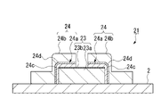
次に、本発明に係る温度センサ及びその製造方法の第2実施形態について、図3を参照して以下に説明する。なお、以下の実施形態の説明において、上記実施形態において説明した同一の構成要素には同一の符号を付し、その説明は省略する。
第2実施形態と第1実施形態との異なる点は、第1実施形態では、第1電極層4aが、Tiだけで形成されているのに対し、第2実施形態の温度センサ21では、図3に示すように、第1電極層24aが、少なくともTiOx層24dを備えている点である。このTiOx層24dは導電性を有しており、薄膜サーミスタ部23と第2電極層4bとの間を電気的に導通させる第1電極層24aとして機能する。
本実施形態では、第1電極層24aが、薄膜サーミスタ部23上に積層されたTi層24cと、Ti層24c上に形成されたTiOx層24dとを備えている。すなわち、ITO層である第2電極層24bは、TiOx層24d上に積層されている。
本実施形態では、第1電極層24aが、薄膜サーミスタ部23上に積層されたTi層24cと、Ti層24c上に形成されたTiOx層24dとを備えている。すなわち、ITO層である第2電極層24bは、TiOx層24d上に積層されている。
なお、第1電極層24a全体が、TiOx層24dであっても構わないが、その場合、導電性を高めるために薄く形成する。
例えば、上記TiOx層24dは、厚さ5nm以下に設定される。なお、厚さ5nmのTiOx層24dの可視光透過率は、80.1%である。
上記TiOx層24dは、TiO2等のTi酸化層であり、低い電気抵抗率を有した導電層である(TiO2の場合、1.2×10²Ωm)。
例えば、上記TiOx層24dは、厚さ5nm以下に設定される。なお、厚さ5nmのTiOx層24dの可視光透過率は、80.1%である。
上記TiOx層24dは、TiO2等のTi酸化層であり、低い電気抵抗率を有した導電層である(TiO2の場合、1.2×10²Ωm)。
さらに、第2実施形態では、薄膜サーミスタ部23が、サーミスタ材料で形成されたサーミスタ層23aと、サーミスタ層23a上に形成されたサーミスタ材料の酸化層23bとを備えている点でも第1実施形態と異なっている。
すなわち、サーミスタ層23aが、一般式:TixAlyNz(0.70≦y/(x+y)≦0.95、0.4≦z≦0.5、x+y+z=1)で示される金属窒化物からなり、その結晶構造が、六方晶系のウルツ鉱型の単相であるサーミスタ材料(TiAlN)で形成されている。そのため、酸化層23bは、このTiAlNのサーミスタ材料が酸化された層、すなわちTiAlNOで形成されている。
なお、酸化層23bは、極薄い層であり、一定の導電性を有しており、絶縁層ではない。したがってサーミスタ層23aと電極部との間を電気的に導通させることが可能である。
すなわち、サーミスタ層23aが、一般式:TixAlyNz(0.70≦y/(x+y)≦0.95、0.4≦z≦0.5、x+y+z=1)で示される金属窒化物からなり、その結晶構造が、六方晶系のウルツ鉱型の単相であるサーミスタ材料(TiAlN)で形成されている。そのため、酸化層23bは、このTiAlNのサーミスタ材料が酸化された層、すなわちTiAlNOで形成されている。
なお、酸化層23bは、極薄い層であり、一定の導電性を有しており、絶縁層ではない。したがってサーミスタ層23aと電極部との間を電気的に導通させることが可能である。
第2実施形態における温度センサ21の製造方法では、サーミスタ形成工程が、サーミスタ材料で形成されたサーミスタ層23aを形成するサーミスタ層工程と、サーミスタ層23aの上面を酸化させてサーミスタ層23a上に酸化層23bを形成する酸化層形成工程とを有している。
上記酸化層形成工程は、サーミスタ層23a形成後にサーミスタ層23aの表面を自然酸化、又は熱処理等によって酸化させることで酸化層23bを形成する。
また、第1電極層24aは、薄膜サーミスタ部23上にTi層24cを積層した後、熱処理等によってTi層24cの表面を酸化させることでTiOx層24dを形成する。
上記酸化層形成工程は、サーミスタ層23a形成後にサーミスタ層23aの表面を自然酸化、又は熱処理等によって酸化させることで酸化層23bを形成する。
また、第1電極層24aは、薄膜サーミスタ部23上にTi層24cを積層した後、熱処理等によってTi層24cの表面を酸化させることでTiOx層24dを形成する。
このように第2実施形態の温度センサ21では、第1電極層24aが、少なくともTiOx層24dを備えているので、Tiよりも可視光透過率が高いTiOx層24dと透明電極層であるITO層により、さらに全体として高い可視光透過率を得ることができる。なお、TiOx層24dは導電性を有し、5nm以下の薄い層とすることで、より高い導電性が得られる。
さらに、薄膜サーミスタ部23が、サーミスタ材料で形成されたサーミスタ層23aと、サーミスタ層23a上に形成されたサーミスタ材料の酸化層23bとを備えているので、酸化層23bも酸素バリア層として機能することで、サーミスタ層23aへの酸素侵入をより抑制することができる。したがって、電気特性として、耐熱試験前後のB定数の変化が抑制され、高い信頼性をもつ薄膜サーミスタ素子が得られる。
また、第2実施形態における温度センサ21の製造方法では、サーミスタ形成工程が、サーミスタ材料で形成されたサーミスタ層23aを形成するサーミスタ層工程と、サーミスタ層23aの上面を酸化させてサーミスタ層23a上に酸化層23bを形成する酸化層形成工程とを有しているので、酸化層23bも酸素バリア層として機能し、第2電極層形成時にサーミスタ層23aに対して雰囲気中の酸素の侵入をさらに抑制することができる。
次に、本発明に係る温度センサについて、上記第1実施形態に基づいて作製した実施例により評価した結果を説明する。
薄膜サーミスタ部には、金属窒化物のサーミスタ材料であるTixAlyNzを用いた。反応性スパッタ法にて、組成比Al/(Ti+Al)=0.85としたTi-Al合金ターゲットを用いて、透明ガラス基板上にTi-Al-N膜(Al0.85Ti0.15N)を膜厚100nm成膜した。
第1電極層には、Tiを用いた。スパッタ法にて、Tiターゲットを用いて、薄膜サーミスタ膜上にTi膜を膜厚5nm成膜した。
なお、薄膜サーミスタ部と第1電極層とは、連続成膜で形成した。
第2電極層には、ITOを用いた。スパッタ法にて、ITOターゲット(組成:90wt%In2O3+10wt%SnO2)を用いて、第1電極層にITO膜を膜厚100nm成膜した。
第1電極層には、Tiを用いた。スパッタ法にて、Tiターゲットを用いて、薄膜サーミスタ膜上にTi膜を膜厚5nm成膜した。
なお、薄膜サーミスタ部と第1電極層とは、連続成膜で形成した。
第2電極層には、ITOを用いた。スパッタ法にて、ITOターゲット(組成:90wt%In2O3+10wt%SnO2)を用いて、第1電極層にITO膜を膜厚100nm成膜した。
Tiの第1電極層を採用した対向電極を設けた本発明の実施例について、150℃100hの耐熱試験前後のB定数を測定した。なお、比較例として、第1電極層を導入せず、第2電極層だけの対向電極を設けたものも同様に測定した。
なお、本発明におけるB定数算出方法は、上述したように25℃と50℃とのそれぞれの抵抗値から以下の式によって求めている。
B定数(K)=ln(R25/R50)/(1/T25-1/T50)
R25(Ω):25℃における抵抗値
R50(Ω):50℃における抵抗値
T25(K):298.15K 25℃を絶対温度表示
T50(K):323.15K 50℃を絶対温度表示
なお、本発明におけるB定数算出方法は、上述したように25℃と50℃とのそれぞれの抵抗値から以下の式によって求めている。
B定数(K)=ln(R25/R50)/(1/T25-1/T50)
R25(Ω):25℃における抵抗値
R50(Ω):50℃における抵抗値
T25(K):298.15K 25℃を絶対温度表示
T50(K):323.15K 50℃を絶対温度表示
これらの結果、比較例では耐熱試験前後のB定数の変動が-5.5%と大きかったのに対し、Ti層を5nm導入した本発明の実施例では、B定数の変動が-0.7%と小さくなり、変動率が抑制されていることがわかる。
次に、第2実施形態の実施例として、薄膜サーミスタ部が、サーミスタ層上に酸化膜を備えたものを作製し、耐熱試験前後のB定数の変動を測定した。
なお、第1電極層は、厚さ5nm,2.5nm,1nmの3種類のTi層とした。
また、第2実施形態の各実施例では、第1実施形態の実施例で行った薄膜サーミスタ部と第1電極層との連続成膜を行わずに、第1電極層成膜前にサーミスタ層の酸化膜形成を行った。
この結果、第1実施形態の上記実施例が、B定数の変動が-0.7%であったのに対し、第2実施形態の各実施例(第1電極層(Ti層)が厚さ5nm,2.5nm,1nmの3種類の実施例)では、それぞれB定数の変動が-0.5%とより小さくなり、変動率がさらに抑制されていることがわかる。さらに、上記3種類の実施例に対して、可視光透過率を測定したところ、第一電極層厚さ5nm,2.5nm,1nmの順に56%,69%,72%となり、第一電極層厚さ2.5nm以下において良好な可視光透過率を示している。
なお、第1電極層は、厚さ5nm,2.5nm,1nmの3種類のTi層とした。
また、第2実施形態の各実施例では、第1実施形態の実施例で行った薄膜サーミスタ部と第1電極層との連続成膜を行わずに、第1電極層成膜前にサーミスタ層の酸化膜形成を行った。
この結果、第1実施形態の上記実施例が、B定数の変動が-0.7%であったのに対し、第2実施形態の各実施例(第1電極層(Ti層)が厚さ5nm,2.5nm,1nmの3種類の実施例)では、それぞれB定数の変動が-0.5%とより小さくなり、変動率がさらに抑制されていることがわかる。さらに、上記3種類の実施例に対して、可視光透過率を測定したところ、第一電極層厚さ5nm,2.5nm,1nmの順に56%,69%,72%となり、第一電極層厚さ2.5nm以下において良好な可視光透過率を示している。
なお、本発明の技術範囲は上記実施形態及び実施例に限定されるものではなく、本発明の趣旨を逸脱しない範囲において種々の変更を加えることが可能である。
例えば、上記実施形態では、一対の対向電極が、薄膜サーミスタ部の上に形成されているが、薄膜サーミスタ部の上下に対向電極を設けて一対の対向電極で薄膜サーミスタ部を上下で挟み込む構造としても構わない。
例えば、上記実施形態では、一対の対向電極が、薄膜サーミスタ部の上に形成されているが、薄膜サーミスタ部の上下に対向電極を設けて一対の対向電極で薄膜サーミスタ部を上下で挟み込む構造としても構わない。
1,21…温度センサ、2…絶縁性基板、3,23…薄膜サーミスタ部、23a…サーミスタ層、23b…酸化層、4…対向電極、4a,24a…第1電極層、4b,24b…第2電極層、24d…TiOx層
Claims (8)
- 絶縁性基板と、
前記絶縁性基板の上に金属窒化物のサーミスタ材料で形成された薄膜サーミスタ部と、
前記薄膜サーミスタ部の上及び下の少なくも一方に互いに対向して形成された一対の対向電極とを備え、
前記対向電極が、互いに積層された第1電極層及び第2電極層を備え、
前記第2電極層が、酸化物を含有し、
前記第1電極層が、前記第2電極層を形成する材料よりも酸素透過性が低い金属又は前記第2電極層を形成する材料よりも酸素透過性が低い金属酸化物で形成されていると共に前記第2電極層と前記薄膜サーミスタ部との間に積層されていることを特徴とする温度センサ。 - 請求項1に記載の温度センサにおいて、
前記絶縁性基板が透明基板であり、
前記第2電極層が、透明電極材料で形成され、
前記薄膜サーミスタ部が、一般式:TixAlyNz(0.70≦y/(x+y)≦0.95、0.4≦z≦0.5、x+y+z=1)で示される金属窒化物からなり、その結晶構造が、六方晶系のウルツ鉱型の単相であり、
前記第1電極層が、Crよりも可視光域の光透過率が高い金属又はCrよりも可視光域の光透過率が高い金属酸化物で形成されていることを特徴とする温度センサ。 - 請求項2に記載の温度センサにおいて、
前記第1電極層が、Tiで形成されていることを特徴とする温度センサ。 - 請求項3に記載の温度センサにおいて、
前記第1電極層が、厚さ2.5nm以下のTiで形成されていることを特徴とする温度センサ。 - 請求項1に記載の温度センサにおいて、
前記第1電極層が、少なくともTiOx層を備え、
前記第2電極層が、前記TiOx層上に積層されたITO層であることを特徴とする温度センサ。 - 請求項1に記載の温度センサにおいて、
前記薄膜サーミスタ部が、前記サーミスタ材料で形成されたサーミスタ層と、
前記サーミスタ層上に形成された前記サーミスタ材料の酸化層とを備えていることを特徴とする温度センサ。 - 請求項1に記載の温度センサの製造方法であって、
絶縁性基板の上に金属窒化物のサーミスタ材料で形成された薄膜サーミスタ部を形成するサーミスタ形成工程と、
前記薄膜サーミスタ部の上に互いに対向した一対の対向電極を形成する対向電極形成工程とを有し、
前記対向電極形成工程が、前記薄膜サーミスタ部上に第1電極層を形成する第1電極層形成工程と、
前記第1電極層上に酸化物を含有した第2電極層を形成する第2電極層形成工程とを有し、
前記第1電極層形成工程で、前記第1電極層を、前記第2電極層を形成する材料よりも酸素透過性が低い金属又は前記第2電極層を形成する材料よりも酸素透過性が低い金属酸化物で形成し、
前記第2電極層形成工程で、前記第2電極層を酸素含有雰囲気中で形成することを特徴とする温度センサの製造方法。 - 請求項7に記載の温度センサの製造方法において、
前記サーミスタ形成工程が、前記サーミスタ材料で形成されたサーミスタ層を形成するサーミスタ層工程と、
前記サーミスタ層の上面を酸化させて前記サーミスタ層上に酸化層を形成する酸化層形成工程とを有していることを特徴とする温度センサの製造方法。
Applications Claiming Priority (3)
| Application Number | Priority Date | Filing Date | Title |
|---|---|---|---|
| JP2020025895 | 2020-02-19 | ||
| JP2021000242A JP2021131379A (ja) | 2020-02-19 | 2021-01-04 | 温度センサ及びその製造方法 |
| JP2021-000242 | 2021-01-04 |
Publications (1)
| Publication Number | Publication Date |
|---|---|
| WO2022145083A1 true WO2022145083A1 (ja) | 2022-07-07 |
Family
ID=77550839
Family Applications (1)
| Application Number | Title | Priority Date | Filing Date |
|---|---|---|---|
| PCT/JP2021/029831 Ceased WO2022145083A1 (ja) | 2020-02-19 | 2021-08-13 | 温度センサ及びその製造方法 |
Country Status (3)
| Country | Link |
|---|---|
| JP (1) | JP2021131379A (ja) |
| TW (1) | TW202227789A (ja) |
| WO (1) | WO2022145083A1 (ja) |
Families Citing this family (1)
| Publication number | Priority date | Publication date | Assignee | Title |
|---|---|---|---|---|
| JPWO2024214593A1 (ja) | 2023-04-10 | 2024-10-17 |
Citations (5)
| Publication number | Priority date | Publication date | Assignee | Title |
|---|---|---|---|---|
| JPS6243324B2 (ja) * | 1981-04-03 | 1987-09-12 | Hitachi Ltd | |
| JPS6459901A (en) * | 1987-08-31 | 1989-03-07 | Tdk Corp | Ptc resistance element |
| JP2010197163A (ja) * | 2009-02-24 | 2010-09-09 | Mitsubishi Materials Corp | 薄膜温度センサ及びその製造方法 |
| JP2019129186A (ja) * | 2018-01-22 | 2019-08-01 | 三菱マテリアル株式会社 | サーミスタ及びその製造方法並びにサーミスタセンサ |
| JP2019138798A (ja) * | 2018-02-13 | 2019-08-22 | 三菱マテリアル株式会社 | 温度センサ |
-
2021
- 2021-01-04 JP JP2021000242A patent/JP2021131379A/ja active Pending
- 2021-08-13 WO PCT/JP2021/029831 patent/WO2022145083A1/ja not_active Ceased
- 2021-08-18 TW TW110130492A patent/TW202227789A/zh unknown
Patent Citations (5)
| Publication number | Priority date | Publication date | Assignee | Title |
|---|---|---|---|---|
| JPS6243324B2 (ja) * | 1981-04-03 | 1987-09-12 | Hitachi Ltd | |
| JPS6459901A (en) * | 1987-08-31 | 1989-03-07 | Tdk Corp | Ptc resistance element |
| JP2010197163A (ja) * | 2009-02-24 | 2010-09-09 | Mitsubishi Materials Corp | 薄膜温度センサ及びその製造方法 |
| JP2019129186A (ja) * | 2018-01-22 | 2019-08-01 | 三菱マテリアル株式会社 | サーミスタ及びその製造方法並びにサーミスタセンサ |
| JP2019138798A (ja) * | 2018-02-13 | 2019-08-22 | 三菱マテリアル株式会社 | 温度センサ |
Also Published As
| Publication number | Publication date |
|---|---|
| TW202227789A (zh) | 2022-07-16 |
| JP2021131379A (ja) | 2021-09-09 |
Similar Documents
| Publication | Publication Date | Title |
|---|---|---|
| JP4692548B2 (ja) | 吸収型多層膜ndフィルターおよびその製造方法 | |
| CN103168285B (zh) | 包括导电图形的触摸面板及其制备方法 | |
| CN104169699B (zh) | 温度传感器及其制造方法 | |
| KR20120098739A (ko) | 광전자소자를 위한 다층 금속성 전극 | |
| JP5782727B2 (ja) | タッチパネルセンサ製造方法およびエッチング方法 | |
| KR20150058088A (ko) | 전도성 구조체 및 이의 제조방법 | |
| CN104204750B (zh) | 温度传感器 | |
| JP6094422B2 (ja) | 温度センサ | |
| KR101681878B1 (ko) | 적층체, 그의 제조방법 및 전자기기 | |
| CN104812927B (zh) | 热敏电阻用金属氮化物材料及其制造方法以及薄膜型热敏电阻传感器 | |
| JP2014070953A (ja) | 温度センサ | |
| WO2022145083A1 (ja) | 温度センサ及びその製造方法 | |
| Howson et al. | Production of transparent electrically conducting films by ion plating | |
| JP2786151B2 (ja) | 酸化バナジウム薄膜及びそれを用いたボロメータ型赤外線センサ | |
| KR20070036058A (ko) | 도파로형 광제어 소자와 그 제조방법 | |
| JP4971618B2 (ja) | 表示用電極パターン製造方法 | |
| JP2989886B2 (ja) | アナログ式タツチパネル | |
| JP4773145B2 (ja) | 増反射膜付きAg又はAg合金反射電極膜及びその製造方法 | |
| CN111240507A (zh) | 导电性薄膜和其图案化方法 | |
| KR101909934B1 (ko) | 플렉서블 디스플레이용 투명 전도성 산화물 다층막, 이를 포함하는 디스플레이 및 그 제조 방법 | |
| JP6096869B2 (ja) | 導電性積層体、パターン配線付き透明導電性積層体、および光学デバイス | |
| JP2022105438A (ja) | 温度センサ及びその製造方法 | |
| JP3924846B2 (ja) | 透明導電フィルム | |
| JP6094421B2 (ja) | 温度センサ | |
| JP2022093237A (ja) | ひずみゲージ |
Legal Events
| Date | Code | Title | Description |
|---|---|---|---|
| 121 | Ep: the epo has been informed by wipo that ep was designated in this application |
Ref document number: 21914944 Country of ref document: EP Kind code of ref document: A1 |
|
| NENP | Non-entry into the national phase |
Ref country code: DE |
|
| 122 | Ep: pct application non-entry in european phase |
Ref document number: 21914944 Country of ref document: EP Kind code of ref document: A1 |