WO2022138693A1 - ガラス基板及びガラス基板の製造方法 - Google Patents
ガラス基板及びガラス基板の製造方法 Download PDFInfo
- Publication number
- WO2022138693A1 WO2022138693A1 PCT/JP2021/047481 JP2021047481W WO2022138693A1 WO 2022138693 A1 WO2022138693 A1 WO 2022138693A1 JP 2021047481 W JP2021047481 W JP 2021047481W WO 2022138693 A1 WO2022138693 A1 WO 2022138693A1
- Authority
- WO
- WIPO (PCT)
- Prior art keywords
- glass substrate
- less
- deflection
- vertical direction
- amount
- Prior art date
- Legal status (The legal status is an assumption and is not a legal conclusion. Google has not performed a legal analysis and makes no representation as to the accuracy of the status listed.)
- Ceased
Links
Images




Classifications
-
- H—ELECTRICITY
- H10—SEMICONDUCTOR DEVICES; ELECTRIC SOLID-STATE DEVICES NOT OTHERWISE PROVIDED FOR
- H10P—GENERIC PROCESSES OR APPARATUS FOR THE MANUFACTURE OR TREATMENT OF DEVICES COVERED BY CLASS H10
- H10P72/00—Handling or holding of wafers, substrates or devices during manufacture or treatment thereof
- H10P72/70—Handling or holding of wafers, substrates or devices during manufacture or treatment thereof for supporting or gripping
- H10P72/74—Handling or holding of wafers, substrates or devices during manufacture or treatment thereof for supporting or gripping using temporarily an auxiliary support
-
- C—CHEMISTRY; METALLURGY
- C03—GLASS; MINERAL OR SLAG WOOL
- C03C—CHEMICAL COMPOSITION OF GLASSES, GLAZES OR VITREOUS ENAMELS; SURFACE TREATMENT OF GLASS; SURFACE TREATMENT OF FIBRES OR FILAMENTS MADE FROM GLASS, MINERALS OR SLAGS; JOINING GLASS TO GLASS OR OTHER MATERIALS
- C03C3/00—Glass compositions
- C03C3/04—Glass compositions containing silica
- C03C3/076—Glass compositions containing silica with 40% to 90% silica, by weight
-
- C—CHEMISTRY; METALLURGY
- C03—GLASS; MINERAL OR SLAG WOOL
- C03B—MANUFACTURE, SHAPING, OR SUPPLEMENTARY PROCESSES
- C03B5/00—Melting in furnaces; Furnaces so far as specially adapted for glass manufacture
- C03B5/16—Special features of the melting process; Auxiliary means specially adapted for glass-melting furnaces
- C03B5/18—Stirring devices; Homogenisation
-
- C—CHEMISTRY; METALLURGY
- C03—GLASS; MINERAL OR SLAG WOOL
- C03B—MANUFACTURE, SHAPING, OR SUPPLEMENTARY PROCESSES
- C03B5/00—Melting in furnaces; Furnaces so far as specially adapted for glass manufacture
- C03B5/16—Special features of the melting process; Auxiliary means specially adapted for glass-melting furnaces
- C03B5/18—Stirring devices; Homogenisation
- C03B5/187—Stirring devices; Homogenisation with moving elements
-
- C—CHEMISTRY; METALLURGY
- C03—GLASS; MINERAL OR SLAG WOOL
- C03C—CHEMICAL COMPOSITION OF GLASSES, GLAZES OR VITREOUS ENAMELS; SURFACE TREATMENT OF GLASS; SURFACE TREATMENT OF FIBRES OR FILAMENTS MADE FROM GLASS, MINERALS OR SLAGS; JOINING GLASS TO GLASS OR OTHER MATERIALS
- C03C3/00—Glass compositions
- C03C3/04—Glass compositions containing silica
- C03C3/076—Glass compositions containing silica with 40% to 90% silica, by weight
- C03C3/078—Glass compositions containing silica with 40% to 90% silica, by weight containing an oxide of a divalent metal, e.g. an oxide of zinc
-
- C—CHEMISTRY; METALLURGY
- C03—GLASS; MINERAL OR SLAG WOOL
- C03C—CHEMICAL COMPOSITION OF GLASSES, GLAZES OR VITREOUS ENAMELS; SURFACE TREATMENT OF GLASS; SURFACE TREATMENT OF FIBRES OR FILAMENTS MADE FROM GLASS, MINERALS OR SLAGS; JOINING GLASS TO GLASS OR OTHER MATERIALS
- C03C3/00—Glass compositions
- C03C3/04—Glass compositions containing silica
- C03C3/076—Glass compositions containing silica with 40% to 90% silica, by weight
- C03C3/083—Glass compositions containing silica with 40% to 90% silica, by weight containing aluminium oxide or an iron compound
-
- C—CHEMISTRY; METALLURGY
- C03—GLASS; MINERAL OR SLAG WOOL
- C03C—CHEMICAL COMPOSITION OF GLASSES, GLAZES OR VITREOUS ENAMELS; SURFACE TREATMENT OF GLASS; SURFACE TREATMENT OF FIBRES OR FILAMENTS MADE FROM GLASS, MINERALS OR SLAGS; JOINING GLASS TO GLASS OR OTHER MATERIALS
- C03C3/00—Glass compositions
- C03C3/04—Glass compositions containing silica
- C03C3/076—Glass compositions containing silica with 40% to 90% silica, by weight
- C03C3/083—Glass compositions containing silica with 40% to 90% silica, by weight containing aluminium oxide or an iron compound
- C03C3/085—Glass compositions containing silica with 40% to 90% silica, by weight containing aluminium oxide or an iron compound containing an oxide of a divalent metal
-
- C—CHEMISTRY; METALLURGY
- C03—GLASS; MINERAL OR SLAG WOOL
- C03C—CHEMICAL COMPOSITION OF GLASSES, GLAZES OR VITREOUS ENAMELS; SURFACE TREATMENT OF GLASS; SURFACE TREATMENT OF FIBRES OR FILAMENTS MADE FROM GLASS, MINERALS OR SLAGS; JOINING GLASS TO GLASS OR OTHER MATERIALS
- C03C3/00—Glass compositions
- C03C3/04—Glass compositions containing silica
- C03C3/076—Glass compositions containing silica with 40% to 90% silica, by weight
- C03C3/083—Glass compositions containing silica with 40% to 90% silica, by weight containing aluminium oxide or an iron compound
- C03C3/085—Glass compositions containing silica with 40% to 90% silica, by weight containing aluminium oxide or an iron compound containing an oxide of a divalent metal
- C03C3/087—Glass compositions containing silica with 40% to 90% silica, by weight containing aluminium oxide or an iron compound containing an oxide of a divalent metal containing calcium oxide, e.g. common sheet or container glass
-
- C—CHEMISTRY; METALLURGY
- C03—GLASS; MINERAL OR SLAG WOOL
- C03C—CHEMICAL COMPOSITION OF GLASSES, GLAZES OR VITREOUS ENAMELS; SURFACE TREATMENT OF GLASS; SURFACE TREATMENT OF FIBRES OR FILAMENTS MADE FROM GLASS, MINERALS OR SLAGS; JOINING GLASS TO GLASS OR OTHER MATERIALS
- C03C3/00—Glass compositions
- C03C3/04—Glass compositions containing silica
- C03C3/076—Glass compositions containing silica with 40% to 90% silica, by weight
- C03C3/089—Glass compositions containing silica with 40% to 90% silica, by weight containing boron
-
- C—CHEMISTRY; METALLURGY
- C03—GLASS; MINERAL OR SLAG WOOL
- C03C—CHEMICAL COMPOSITION OF GLASSES, GLAZES OR VITREOUS ENAMELS; SURFACE TREATMENT OF GLASS; SURFACE TREATMENT OF FIBRES OR FILAMENTS MADE FROM GLASS, MINERALS OR SLAGS; JOINING GLASS TO GLASS OR OTHER MATERIALS
- C03C3/00—Glass compositions
- C03C3/04—Glass compositions containing silica
- C03C3/076—Glass compositions containing silica with 40% to 90% silica, by weight
- C03C3/089—Glass compositions containing silica with 40% to 90% silica, by weight containing boron
- C03C3/091—Glass compositions containing silica with 40% to 90% silica, by weight containing boron containing aluminium
-
- C—CHEMISTRY; METALLURGY
- C03—GLASS; MINERAL OR SLAG WOOL
- C03C—CHEMICAL COMPOSITION OF GLASSES, GLAZES OR VITREOUS ENAMELS; SURFACE TREATMENT OF GLASS; SURFACE TREATMENT OF FIBRES OR FILAMENTS MADE FROM GLASS, MINERALS OR SLAGS; JOINING GLASS TO GLASS OR OTHER MATERIALS
- C03C3/00—Glass compositions
- C03C3/04—Glass compositions containing silica
- C03C3/076—Glass compositions containing silica with 40% to 90% silica, by weight
- C03C3/089—Glass compositions containing silica with 40% to 90% silica, by weight containing boron
- C03C3/091—Glass compositions containing silica with 40% to 90% silica, by weight containing boron containing aluminium
- C03C3/093—Glass compositions containing silica with 40% to 90% silica, by weight containing boron containing aluminium containing zinc or zirconium
-
- C—CHEMISTRY; METALLURGY
- C03—GLASS; MINERAL OR SLAG WOOL
- C03C—CHEMICAL COMPOSITION OF GLASSES, GLAZES OR VITREOUS ENAMELS; SURFACE TREATMENT OF GLASS; SURFACE TREATMENT OF FIBRES OR FILAMENTS MADE FROM GLASS, MINERALS OR SLAGS; JOINING GLASS TO GLASS OR OTHER MATERIALS
- C03C3/00—Glass compositions
- C03C3/04—Glass compositions containing silica
- C03C3/076—Glass compositions containing silica with 40% to 90% silica, by weight
- C03C3/095—Glass compositions containing silica with 40% to 90% silica, by weight containing rare earths
-
- H—ELECTRICITY
- H10—SEMICONDUCTOR DEVICES; ELECTRIC SOLID-STATE DEVICES NOT OTHERWISE PROVIDED FOR
- H10W—GENERIC PACKAGES, INTERCONNECTIONS, CONNECTORS OR OTHER CONSTRUCTIONAL DETAILS OF DEVICES COVERED BY CLASS H10
- H10W70/00—Package substrates; Interposers; Redistribution layers [RDL]
- H10W70/60—Insulating or insulated package substrates; Interposers; Redistribution layers
-
- H—ELECTRICITY
- H10—SEMICONDUCTOR DEVICES; ELECTRIC SOLID-STATE DEVICES NOT OTHERWISE PROVIDED FOR
- H10W—GENERIC PACKAGES, INTERCONNECTIONS, CONNECTORS OR OTHER CONSTRUCTIONAL DETAILS OF DEVICES COVERED BY CLASS H10
- H10W74/00—Encapsulations, e.g. protective coatings
- H10W74/01—Manufacture or treatment
- H10W74/019—Manufacture or treatment using temporary auxiliary substrates
Definitions
- the present invention relates to a glass substrate and a method for manufacturing a glass substrate.
- a glass substrate may be used as a member to support the semiconductor device.
- Patent Document 1 describes a glass support substrate for a fan-out wafer level package.
- the present invention has been made in view of the above problems, and an object of the present invention is to provide a glass substrate and a method for manufacturing a glass substrate capable of appropriately manufacturing a semiconductor device.
- the glass substrate according to the present disclosure is a glass substrate for manufacturing a semiconductor device, and one surface of the glass substrate is directed downward in the vertical direction.
- the height in the vertical direction of the other surface is the lowest.
- the lowest point, which is the position, is radially inside the first position, the second position, and the third position when viewed from the vertical direction, and the center is the center point of the glass substrate and the diameter is It is located in a circular central region having a length of 1/3 with respect to the diameter of the glass substrate.
- the method for manufacturing a glass substrate according to the present disclosure is the method for manufacturing a glass substrate, in which a step of melting a raw material and a stirring of the melted raw material are performed. It includes a step of stirring under the conditions of a rotation speed of 5 rpm or more and 20 rpm or less and 12 hours or more and 24 hours or less, and a step of cooling the stirred raw material to form the glass substrate.
- a semiconductor device can be appropriately manufactured.
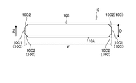
- FIG. 1A is a schematic view of a glass substrate according to this embodiment.
- FIG. 1B is a schematic view of a glass substrate according to this embodiment.
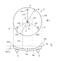
- FIG. 2A is a schematic diagram for explaining the deflection of the glass substrate according to the present embodiment.
- FIG. 2B is a schematic diagram for explaining the deflection of the glass substrate according to the present embodiment.
- FIG. 3A is a schematic diagram for explaining the deflection of the glass substrate according to the present embodiment.
- FIG. 3B is a schematic diagram for explaining the deflection of the glass substrate according to the present embodiment.
- FIG. 4 is a flowchart illustrating a method for manufacturing a glass substrate according to the present embodiment.
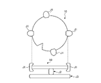
- FIG. 5 is a diagram illustrating an evaluation method of each example.
- FIG. 6 is a graph showing an example of dy / dF.
- Glass substrate 1A and 1B are schematic views of a glass substrate according to the present embodiment.
- 1A is a front view of the glass substrate 10 according to the present embodiment
- FIG. 1B is a plan view of the glass substrate 10 according to the present embodiment.
- the glass substrate 10 according to the present embodiment is used as a glass substrate for manufacturing a semiconductor package, and can be said to be a glass substrate that supports a semiconductor device.
- the glass substrate 10 is a support glass substrate for manufacturing a fan-out wafer level package (FOWLP).
- FOWLP fan-out wafer level package
- FOPLP Fan Out Panel Level Package
- the use of the glass substrate 10 is not limited to supporting semiconductor devices and manufacturing FOWLP and FOPLP, and may be any glass substrate used to support any member.
- the glass substrate 10 has a surface 10A (one surface) which is one main surface and a surface 10B (the other surface) which is a main surface opposite to the surface 10A. It is a plate-shaped member. As shown in FIG. 1B, the glass substrate 10 has a circular disk shape when viewed in a plan view, that is, when viewed from a direction orthogonal to the surface 10A. In other words, the glass substrate 10 has a wafer shape.
- the glass substrate 10 may have a notch portion 10D (notch) formed on the outer peripheral surface 10C so that the outer peripheral surface of the circle is partially cut out.
- the notch portion 10D may also have a chamfered shape including the outer peripheral surface portion 14C1 and the edge surface portion 14C2, which will be described later.
- the shape of the glass substrate 10 is not limited to the disk shape, but may be any shape, and may be a polygonal plate such as a rectangle.
- the direction orthogonal to the surface 10A is referred to as the Z direction.
- the Z direction can also be said to be the thickness direction of the glass substrate 10.
- the glass substrate 10 is chamfered on the outer peripheral surface 10C.
- the outer peripheral surface 10C includes an outer peripheral surface portion 10C1 and an edge surface portion 10C2.
- the outer peripheral surface portion 10C1 corresponds to the unchamfered portion of the outer peripheral surface 10C
- the edge surface portion 10C2 corresponds to the chamfered portion of the outer peripheral surface 10C.
- the outer peripheral surface 10C has a shape including the outer peripheral surface portion 10C1 and the edge surface portion 10C2 as shown in FIG. 1A over the entire peripheral direction of the glass plate 10.
- the outer peripheral surface portion 10C1 is a surface of the outer peripheral surface 10C including the portion most protruding outward in the radial direction of the glass plate 10. As shown in FIG. 1A, the outer peripheral surface portion 10C1 is along the Z direction when viewed from a direction orthogonal to the Z direction.
- the outer peripheral surface portion 10C1 is connected to the surface of the glass substrate 10 via the edge surface portion 10C2. That is, one end of the edge surface portion 10C2 in the Z direction is connected to the outer peripheral surface portion 10C1, and the other end is connected to the surface of the glass substrate 10.
- the edge surface portion 10C2 is formed on both sides of the outer peripheral surface portion 10C1 in the Z direction. That is, the outer peripheral surface 10C is formed so as to be arranged in the Z direction in the order of one edge surface portion 10C2, the outer peripheral surface portion 10C1, and the other edge surface portion 10C2.
- One end of the edge surface portion 10C2 in the Z direction is connected to the surface 10A of the glass substrate 10, and the other end is connected to the outer peripheral surface portion 10C1. Further, one end of the other edge surface portion 10C2 in the Z direction is connected to the outer peripheral surface portion 10C1, and the other end portion is connected to the surface 10B of the glass substrate 10.
- the edge surface portion 10C2 is inclined with respect to the Z direction when viewed from a direction orthogonal to the Z direction.
- the edge surface portion 10C2 is inclined so as to be inward in the radial direction of the glass substrate 10 from the outer peripheral surface portion 10C1 toward the surface side of the glass substrate 10.
- the outer peripheral surface 10C has a shape in which a chamfer is formed including the outer peripheral surface portion 10C1 and the edge surface portion 10C2, but the shape of the outer peripheral surface 10C is not limited to this, and for example, a chamfer is formed. It does not have to be.
- the diameter W of the glass substrate 10 is preferably 150 mm or more and 700 mm or less, more preferably 150 mm or more and 450 mm or less, further preferably 150 mm or more and 400 mm or less, and further preferably 250 mm or more and 350 mm or less. , 300 mm or more and 350 mm or less is more preferable. When the diameter W is in this range, a member such as a semiconductor device can be appropriately supported.
- the diameter W is the diameter when the glass substrate 10 is circular, but when the glass substrate 10 is not circular, the diameter W is the distance between any two points on the outer peripheral edge of the glass substrate 10. You may point to the maximum value.
- the thickness D of the glass substrate 10, that is, the length between the surface 10A and the surface 10B is preferably 2 mm or less, more preferably 0.5 mm or more and 2.0 mm or less, and 0.6 mm or more 1 It is more preferably 5.5 mm or less, and further preferably 0.6 mm or more and 1.0 mm or less.
- the glass substrate 10 is preferable as a semiconductor device manufacturing application because the weight increase due to the large thickness is suppressed.
- the thickness D falls within this range, there is a high possibility that the semiconductor device cannot be properly manufactured due to the influence of the deflection.
- the position of the lowest point due to the deflection by its own weight is set to the center side. As a result, deterioration of the manufacturability of the semiconductor device can be suppressed.
- the deviation of the thickness D is preferably 10 ⁇ m or less, and more preferably 3 ⁇ m or less.
- the deviation of the thickness D refers to the deviation of the thickness D (for each coordinate) for each position on the plane along the surface of the glass substrate 10. For example, the thickness D at each position (coordinates) on the plane along the surface of the glass substrate 10 is calculated, and the difference between the maximum value and the minimum value in the thickness D for each position is calculated as the thickness. It may be a deviation of D.
- the Young's modulus of the glass substrate 10 is preferably 60 GPa or more and 150 GPa or less, more preferably 70 GPa or more and 120 GPa or less, and further preferably 75 GPa or more and 100 GPa or less.
- the Young's modulus is in this range, the decrease in rigidity of the glass substrate can be suppressed and the shape change of the glass substrate can be suppressed, so that the deterioration of the manufacturability of the semiconductor device can be suppressed.
- the Young's modulus of the glass substrate 10 a value measured based on the propagation of ultrasonic waves using 38DL PLUS manufactured by OLYMPUS may be used.
- the density of the glass substrate 10 is preferably 2.0 g / cm 3 or more and 4.0 g / cm 3 or less, and more preferably 2.5 g / cm 3 or more and 3.3 g / cm 3 or less. When the density is in this range, it is possible to suppress an increase in the weight of the glass substrate 10 and suppress deterioration in the manufacturability of the semiconductor device.
- the density of the glass substrate 10 may be a value measured by using the Archimedes method.
- the glass substrate 10 preferably contains the following compounds in mass% (wt%) based on the oxide.
- the member can be appropriately supported.
- SiO 2 40 wt% or more and 75 wt% or less is preferable, 50 wt% or more and 75 wt% or less is more preferable.
- Al 2 O 3 0 wt% or more and 20 wt% or less is preferable, and 0 wt% or more and 15 wt% or less is more preferable.
- B 2 O 3 0 wt% or more and 20 wt% or less is preferable, 0 wt% or more and 10 wt% or less is more preferable MgO: 0 wt% or more and 25 wt% or less is preferable CaO: 0 wt% or more and 25 wt% or less is preferable, 0 wt% or more More preferably 15 wt% or less SrO: preferably 0 wt% or more and 10 wt% or less BaO: preferably 0 wt% or more and 20 wt% or less, more preferably 0 wt% or more and 15 wt% or less Li 2 O: 0 wt% or more and 40 wt % Or less is preferable Na 2 O: 0 wt% or more and 15 wt% or less is preferable K 2 O: 0 wt% or more and 10 wt% or less is preferable ZrO 2 : 0 wt%
- 0 wt% or more and 5 wt% or less are further preferable.
- TiO 2 0 wt% or more and 5 wt% or less are preferable.
- Y 2 O 3 0 wt% or more and 10 wt% or less are preferable.
- FIG. 2A and 2B are schematic views for explaining the deflection of the glass substrate according to the present embodiment.
- FIG. 2A shows a case where the first position P1A, the second position P2A, and the third position P3A, which are radially outside the center point O of the glass substrate 10 when viewed from the Z direction, are supported at three points by the support member B. It is a figure explaining the example of the deflection by the own weight of.
- the first position P1A is a position on the surface 10A separated from the center point O of the glass substrate 10 by a distance L1A outward in the radial direction.
- the second position P2A is a position on the surface 10A separated from the center point O of the glass substrate 10 in the radial direction by a distance L2A, and is relative to the first position P1A when the center point O is the center. It is a position shifted by 120 degrees in the circumferential direction.
- the third position P3A is a position on the surface 10A separated from the center point O of the glass substrate 10 in the radial direction by a distance L3A, and is the first position P1A and the second position when the center point O is the center. It is a position shifted by 120 degrees in the circumferential direction with respect to the position P2A.
- the radial direction here refers to the radial direction when the center point O is the center.
- the distance L1A, the distance L2A, and the distance L3A have the same length as each other, and are 29/30 times as long as half (radius) of the diameter W of the glass substrate 10.
- the support member B is a spherical member having a diameter of 1 mm or more and 2 mm or less, and more preferably 1.6 mm in diameter.
- the material of the support member B is preferably a material that is softer than glass and is not easily deformed by temperature and humidity or the weight of glass during measurement, and is, for example, a resin such as PEEK (Polyetheretherketone) or PTFE (Polyetherketone). , Here PEEK may be used.
- the position where the height in the vertical direction is the lowest is defined as the lowest point SB1. That is, it can be said that the lowest point SB1 is the position where the amount of deflection is the largest in the surface 10B.
- the position of the lowest point SB1 is located in the central region AR when viewed from the vertical direction (Z direction).
- the central region AR is a region radially inside the first position P1A, the second position P2A, and the third position P3A. Further, the central region AR is a circular region whose center is the center point O and whose diameter D1 is 1/3 of the diameter W of the glass substrate 10.
- the glass substrate 10 has the lowest point when the surface 10A is directed downward in the vertical direction and the first position P1A, the second position P2A, and the third position P3A of the surface 10A are supported by the support member B at three points.
- SB is located in the central region AR.
- the lowest point SB is located in the central region AR instead of the outside of the central region AR, so that deformation of the glass substrate 10 such that the bending position of the glass substrate 10 is displaced during manufacturing of the semiconductor device is suppressed, and the semiconductor device is not deformed. Deterioration of manufacturability can be suppressed.
- the maximum of the glass substrate 10 when the surface 10A of the glass substrate 10 is directed downward in the vertical direction and the first position P1A, the second position P2A, and the third position P3A on the surface 10A are supported by the support member B.
- the amount of deflection is defined as the maximum amount of deflection TBmax.
- the maximum amount of deflection TBmax can be said to be the maximum amount of deflection due to the weight of the glass substrate 10, and can be said to be the distance along the vertical direction from the highest point SB2 to the lowest point SB1 of the glass substrate 10.
- the highest point SB2 is a case where the surface 10A of the glass substrate 10 is directed downward in the vertical direction and the first position P1A, the second position P2A, and the third position P3A on the surface 10A are supported by the support member B. This is the position where the height in the vertical direction is the highest among the surface 10B on the upper side in the vertical direction.
- the maximum deflection amount TBmax is preferably 650 ⁇ m or less, and preferably 10 ⁇ m or more and 630 ⁇ m or less. Is more preferable, and more preferably 50 ⁇ m or more and 625 ⁇ m or less.
- the maximum amount of deflection TBmax is in this range, the amount of deflection is also suppressed, so that deterioration of the manufacturability of the semiconductor device can be more preferably suppressed.
- the maximum amount of deflection TBmax can be measured by a Dyvoce manufactured by Kozu Seiki.
- FIG. 2A illustrates an example in which the glass substrate 10 is simply warped, but the warping of the glass substrate 10 is not limited to the simple warping as shown in FIG. 2A, and the warping method as shown in FIG. 2B, for example. It may be. That is, in FIG. 2A, the glass substrate 10 is bent so as to have a concave shape recessed from the outer peripheral end toward the lowest point SB1, but as shown in FIG. 2B, the lowest point is from the position indicated by the support member B. It may be dented toward SB1 and may be bent so as to be dented from a portion supported by the support member B toward the outer peripheral end.
- FIG. 3A shows a case where the first position P1B, the second position P2B, and the third position P3B, which are radially outside the center point O of the glass substrate 10 when viewed from the Z direction, are supported at three points by the support member B. It is a figure explaining the example of the deflection by the own weight of.
- the first position P1B is a position on the surface 10B separated from the center point O of the glass substrate 10 by a distance L1B outward in the radial direction.
- the second position P2B is a position on the surface 10B separated radially outward from the center point O of the glass substrate 10 by a distance L2B, and is relative to the first position P1B when the center point O is the center. It is a position shifted by 120 degrees in the circumferential direction.
- the third position P3B is a position on the surface 10B separated from the center point O of the glass substrate 10 by a distance L3B outward in the radial direction, and is the first position P1B and the second position when the center point O is the center.
- the distance L1B, the distance L2B, and the distance L3B have the same length as each other, and are 29/30 times as long as half (radius) of the diameter W of the glass substrate 10.
- the position where the height in the vertical direction is the lowest among the surface 10A on the upper side in the vertical direction is defined as the lowest point SA1. That is, it can be said that the lowest point SA1 is the position where the amount of deflection is the largest in the surface 10A. In this case, the position of the lowest point SA1 is preferably located in the central region AR when viewed from the vertical direction (Z direction).
- FIG. 3A illustrates an example in which the glass substrate 10 is simply warped, but the warping of the glass substrate 10 is not limited to the simple warping as shown in FIG. 3A, and the warping method as shown in FIG. 3B, for example. It may be. That is, in FIG. 3A, the glass substrate 10 is bent so as to have a concave shape recessed from the outer peripheral end toward the lowest point SA1, but as shown in FIG. 3B, the lowest point is from the position indicated by the support member B. It may be dented toward SA1 and may be bent so as to be dented from a portion supported by the support member B toward the outer peripheral end.
- the glass substrate 10 has a minimum point SB1 (see FIG. 2A) when the surface 10A is supported at three points downward in the vertical direction and a minimum point when the surface 10B is supported at three points downward in the vertical direction. Both with point SA1 (see FIG. 3A) are located within the central region AR. However, in the glass substrate 10, at least one of the lowest points SB1 and SA1 may be located in the central region AR, and for example, one of the lowest points SB1 and SA1 may be located outside the central region AR. ..
- the maximum of the glass substrate 10 when the surface 10B of the glass substrate 10 is directed downward in the vertical direction and the first position P1B, the second position P2B, and the third position P3B on the surface 10B are supported by the support member B.
- the amount of deflection is defined as the maximum amount of deflection TAmax.
- the maximum amount of deflection TAmax can be said to be the maximum amount of deflection due to the weight of the glass substrate 10, and can be said to be the distance along the vertical direction from the highest point SA2 to the lowest point SA1 of the glass substrate 10.
- the highest point SA2 is a case where the surface 10B of the glass substrate 10 is directed downward in the vertical direction and the first position P1B, the second position P2B, and the third position P3B on the surface 10B are supported by the support member B. This is the position where the height in the vertical direction is the highest among the surface 10A on the upper side in the vertical direction.
- the maximum deflection amount TAmax is preferably 650 ⁇ m or less, and preferably 10 ⁇ m or more and 630 ⁇ m or less. Is more preferable, and more preferably 50 ⁇ m or more and 625 ⁇ m or less.
- the deflection amount TAmax is also suppressed, so that deterioration of the manufacturability of the semiconductor device can be more preferably suppressed.
- the maximum amount of deflection TAmax can be measured with a Dyvoce manufactured by Kozu Seiki.
- the larger value is defined as the maximum deflection amount Tmax. ..
- the value obtained by multiplying the maximum deflection amount Tmax by the cube of the thickness D of the glass substrate 10 and the Young's modulus E of the glass substrate 10 and dividing by 1000 (that is, Tmax ⁇ D 3 ⁇ E / 1000) is 20 or less. Is preferable.
- the amount of warpage of the glass substrate 10 when the deflection due to its own weight is removed is defined as the amount of warpage ⁇ T.
- the warp amount ⁇ T is preferably 250 ⁇ m or less, and more preferably 100 ⁇ m or less.
- the semiconductor device manufactured on the glass substrate 10 can be suppressed from warping, and the deterioration of the manufacturability of the semiconductor device can be more preferably suppressed.
- the amount of warp ⁇ T is the case where the surface 10B is supported by the support member B as described above with the surface 10B facing downward in the vertical direction and the case where the surface 10A is supported with the supporting member B as described above with the surface 10A facing downward in the vertical direction.
- the maximum value of the difference in the amount of deflection (for each coordinate) for each position on the plane along the surface of the glass substrate 10 is divided by 2. That is, the amount of deflection at the position (coordinates) i on the plane along the surface of the glass substrate 10 when the surface 10B is supported by the support member B as described above with the surface 10B facing downward in the vertical direction is defined as TA (i) .
- the amount of deflection at the position (coordinates) i on the plane along the surface of the glass substrate 10 when the surface 10A is supported by the support member B as described above with the surface 10A facing downward in the vertical direction is defined as TB (i) . ..
- the one having the maximum value is defined as MAX (TA (i) -TB (i) ).
- the warp amount ⁇ T is obtained by the following equation (1). That is, the warp amount ⁇ T is a value obtained by dividing the absolute value of MAX (TA (i) ⁇ TB (i) ) by 2.
- FIG. 4 is a flowchart illustrating a method for manufacturing a glass substrate according to the present embodiment.
- the raw material adjusted according to the composition of the glass substrate 10 is heated and melted (step S10).
- the dissolved raw material is stirred (step S12).
- the stirring conditions for the raw materials are arbitrary, but for example, it is preferable to stir for 12 hours or more and 24 hours or less, with the rotation speed of the stirring blade for stirring the melted raw materials being 5 rpm or more and 20 rpm or less.
- the stirring blade is a member for stirring the melted raw material, and may have any shape, and is not limited to, for example, a blade shape.
- the glass substrate 10 can be manufactured without stirring the melted raw material in this way, but by stirring in this way, it is possible to suppress the occurrence of an abnormality in the bending shape. ,preferable.
- the step of forming the glass substrate 10 may be any method, and for example, the glass substrate 10 may be formed by cutting out the ingod after manufacturing the glass ingod. In this case, for example, the ingod may be manufactured by a melt casting method. Further, for example, the plate-shaped glass substrate 10 may be directly formed without manufacturing a glass ingod. In this case, for example, the plate-shaped glass substrate 10 may be manufactured by a roll-out method, a down-draw method, a fusion method, a float method, or the like. In any of the methods, a step of polishing the surface of the glass may be added.
- the glass substrate 10 according to the present embodiment is for manufacturing a semiconductor device, and one surface 10A is directed downward in the vertical direction, and the center point O of the glass substrate 10 of the one surface 10A is directed downward.
- the first position P1A, the second position P2A, and the third position P3A on the outer side in the radial direction are supported by the support member B, the position where the height in the vertical direction is the lowest among the other surfaces 10B.
- the lowest point SB1 is located in the central region AR when viewed from the vertical direction.
- the central region AR is radially inside the first position P1A, the second position P2A, and the third position P3A, and the center is the center point O of the glass substrate 10 and the diameter D1 is the diameter of the glass substrate 10. It is a circular region having a length of 1/3 with respect to W.
- a temperature difference may occur between processes, and stress may be generated on the glass substrate due to a difference in the coefficient of thermal expansion between materials. The stress causes the glass substrate to deform, but the deformation may be discontinuous. If the deformation of the glass substrate is discontinuous, contact between the equipment and the glass substrate or disconnection of the device due to a sudden change in shape may occur.
- the glass substrate 10 according to the present embodiment since the lowest point SB1 at which the self-weight deflection is maximum is located in the central region AR, the bending position of the glass substrate 10 is determined by a load when supporting the semiconductor device or the like. Discontinuous deformation such as shifting is suppressed. Therefore, according to the glass substrate 10 according to the present embodiment, it is possible to appropriately manufacture the semiconductor device by suppressing the deterioration of the manufacturability of the semiconductor device.
- the other surface 10B is directed downward in the vertical direction, and the first position P1B, the second position P2B, and the second position P2B on the other surface 10B are radially outside the center point O of the glass substrate 10.
- the lowest point SA1 which is the position where the height in the vertical direction is the lowest among the one surface 10A, is located in the central region AR when viewed from the vertical direction. It is preferable to do so.
- the lowest points SA1 and SB1 that maximize the deflection by their own weight are located in the central region AR regardless of which of the surfaces 10A and 10B is directed downward. Therefore, according to the glass substrate 10, deformation such that the bending position of the glass substrate 10 is displaced is further suppressed, and a semiconductor device can be more preferably manufactured.
- the glass substrate 10 preferably has a thickness D of 2 mm or less.
- the thickness D of the glass substrate 10 is a glass substrate by locating the lowest point SB1 in the central region AR. It is possible to suppress deformation such that the bending position of 10 is displaced, and to suppress deterioration of manufacturability of the semiconductor device.
- the glass substrate 10 has a diameter W of 150 mm or more and 700 mm or less, and one surface 10A is directed downward in the vertical direction to support the first position P1A, the second position P2A, and the third position P3A of the one surface 10A.
- the maximum deflection amount TBmax is preferably 650 ⁇ m or less.
- the maximum amount of deflection TBmax when one surface 10A of the glass substrate 10 is directed downward in the vertical direction and the first position P1A, the second position P2A, and the third position P3A of the one surface 10A are supported by the support member B.
- the maximum amount of deflection TAmax when the other surface 10B is directed downward in the vertical direction and the first position P1B, the second position P2B, and the third position P3B of the other surface 10B are supported by the support member B.
- Tmax the thickness of the glass substrate 10 is D
- the Young's modulus of the glass substrate 10 it is preferable that Tmax ⁇ D 3 ⁇ E / 1000 ⁇ 20.
- the glass substrate 10 when the other surface 10B of the glass substrate 10 is directed downward in the vertical direction and the first position P1B, the second position P2B, and the third position P3B of the other surface 10B are supported by the support member B, the glass substrate 10
- the maximum deflection amount TAmax is preferably 650 ⁇ m or less.
- the portion (edge surface portion 14C2) between the surface and the outer peripheral surface 10C of the glass substrate 10 is chamfered. Since the glass substrate 10 is chamfered, a semiconductor device can be more preferably manufactured.
- the glass substrate 10 has a notch portion 10D formed on the outer peripheral surface 10C.
- the semiconductor device can be more preferably manufactured by appropriately performing positioning and the like.
- the glass substrate 10 has a warp amount ⁇ T of 250 ⁇ m or less and a deviation of the thickness D of 10 ⁇ m or less when the deflection due to its own weight is removed.
- the deviation between the warp amount ⁇ T and the thickness D of the glass substrate 10 is within this range, it is possible to suppress deformation such that the bending position of the glass substrate 10 is displaced, and to suppress deterioration of the manufacturability of the semiconductor device.
- the warp amount ⁇ T of the glass substrate 10 excluding the deflection due to its own weight is 100 ⁇ m or less, and the deviation of the thickness D is 3 ⁇ m or less.
- the deviation between the warp amount ⁇ T and the thickness D of the glass substrate 10 is within this range, it is possible to suppress deformation such that the bending position of the glass substrate 10 is displaced, and to suppress deterioration of the manufacturability of the semiconductor device.
- the glass substrate 10 is based on the oxide mass%. SiO 2 : 40 wt% or more and 75 wt% or less, Al 2 O 3 : 0 wt% or more and 20 wt% or less, B 2 O 3 : 0 wt% or more and 20 wt% or less, MgO: 0 wt% or more and 25 wt% or less, CaO: 0 wt% or more and 25 wt% or less, SrO: 0 wt% or more and 10 wt% or less, BaO: 0 wt% or more and 20 wt% or less, Li 2 O: 0 wt% or more and 40 wt% or less, Na 2 O: 0 wt% or more and 15 wt% or less, K 2 O: 0 wt% or more and 10 wt% or less, ZrO 2 : 0 wt% or more and 10 wt% or less, TiO 2 : 40
- the glass substrate 10 is preferably a glass substrate for manufacturing at least one of a fan-out wafer level package and a fan-out panel level package.
- the glass substrate 10 is suitable for use in fan-out wafer level packages and fan-out panel level packages.
- the method for manufacturing the glass substrate 10 includes a step of melting the raw material and a step of stirring the melted raw material under the conditions of stirring rotation speed of 5 rpm or more and 20 rpm or less and 12 hours or more and 24 hours or less. , A step of cooling the stirred raw material to form the glass substrate 10.
- this manufacturing method by stirring the melted raw materials, it is possible to make the raw materials uniform, suppress deformation such that the bending position of the glass substrate 10 is displaced, and glass capable of suitably manufacturing a semiconductor device.
- the substrate 10 can be provided.
- Table 1 shows the glass substrate of each example.
- the raw materials were adjusted so that the glass substrate had a predetermined composition, and the glass substrate was manufactured. Then, the Young's modulus, the density, the position of the lowest point in the self-weight deflection, and the amount of deflection were measured with respect to the manufactured glass substrate. Young's modulus was measured using 38DL PLUS manufactured by OLYMPUS, and density was measured by the Archimedes method. Further, in the measurement of the position of the lowest point and the measurement of the amount of deflection, the present implementation is carried out so that the second surface, which is the other surface of the glass substrate, is vertically downward and above the first surface, which is one surface of the glass substrate.
- the first position P1A, the second position P2A, and the third position P3A described in the embodiment were supported by the support member B. Then, in that case, the position of the lowest point on the first surface where the height in the vertical direction is the lowest is measured, and the measurement result is set as "on the first surface" of the "position of the lowest point” in Table 1. Indicated. In Table 1, when the position of the lowest point is in the central region AR shown in the present embodiment, the position of the lowest point is defined as “inside” and the position of the lowest point is the central region shown in the present embodiment. The position of the lowest point was defined as "outside" when it was not in the AR (when it was outside the central region AR).
- the amount of deflection when the glass substrate is supported as described above, the amount of deflection at each position on the first surface is measured, and the minimum to maximum values are calculated from the minimum value on the first surface in Table 1. "Deflection”. A Dyvoce manufactured by Kozu Seiki was used to measure the amount of deflection. Further, the first position P1B, the second position P2B, and the third position P3B described in this embodiment are placed on the first surface, which is one surface, in the vertical direction and above the second surface, which is the other surface. It was supported by the support member B.
- the position of the lowest point on the second surface where the height in the vertical direction is the lowest is measured, and the measurement result is "on the second surface" of the "position of the lowest point” in Table 1.
- the position of the lowest point is defined as “inside” and the position of the lowest point is the central region shown in the present embodiment.
- the position of the lowest point was defined as "outside” when it was not in the AR (when it was outside the central region AR).
- the amount of deflection when the glass substrate is supported as described above, the amount of deflection at each position on the second surface is measured, and the minimum to maximum values are calculated from the "second" in Table 1.
- the "maximum deflection amount” in Table 1 is the maximum value among the “deflection on the first surface” and the “deflection on the second surface”, and the warp amount is as in the above equation (1). It is a calculated value. Further, “Tmax ⁇ D 3 ⁇ E / 1000" in Table 1 is a value obtained by multiplying the maximum amount of deflection by the cube of "thickness” and "Young's modulus” and dividing by 1000.
- Example 1 In Example 1, the raw materials are adjusted so that the glass substrate has a predetermined composition C1, the raw materials are melted, the melted raw materials are stirred, a glass ingod is manufactured, and the ingod is machined to have a diameter. , A glass substrate having the thickness, Young's modulus, density, position of the lowest point, and the amount of deflection as shown in Table 1 was manufactured.
- Example 2 In Example 2, the raw materials are adjusted so that the glass substrate has the composition C1, the raw materials are melted, the melted raw materials are agitated, a glass ingod is manufactured, and the ingod is machined to have a diameter and a thickness. , Young's modulus, density, position of the lowest point, and the amount of deflection are as shown in Table 1.
- Example 3 In Example 3, the raw material is adjusted so that the glass substrate has the composition C1, the raw material is melted, the melted raw material is stirred, a glass ingod is manufactured, and the ingod is machined to obtain the diameter and thickness. , Young's modulus, density, position of the lowest point, and the amount of deflection are as shown in Table 1.
- Example 4 In Example 4, the raw materials are adjusted so that the glass substrate has the composition C1, the raw materials are melted, the melted raw materials are stirred, and a plate-shaped glass substrate is manufactured, and the diameter, thickness, Young's modulus, and density are obtained. , A glass substrate having the position of the lowest point and the amount of deflection as shown in Table 1 was manufactured.
- Example 5 In Example 5, the raw materials are adjusted so that the glass substrate has a predetermined composition C2, the raw materials are melted and the melted raw materials are stirred to produce a plate-shaped glass substrate, and the diameter, thickness, Young's modulus, and so on. A glass substrate having the density, the position of the lowest point, and the amount of deflection as shown in Table 1 was manufactured.
- Example 6 the raw materials are adjusted so that the glass substrate has a predetermined composition C3, the raw materials are melted and the melted raw materials are stirred to produce a plate-shaped glass substrate, and the diameter, thickness, Young's modulus, and so on. A glass substrate having the density, the position of the lowest point, and the amount of deflection as shown in Table 1 was manufactured.
- Example 7 In Example 7, the raw materials are adjusted so that the glass substrate has a predetermined composition C4, the raw materials are melted and the melted raw materials are stirred to produce a plate-shaped glass substrate, and the diameter, thickness, Young's modulus, and so on. A glass substrate having the density, the position of the lowest point, and the amount of deflection as shown in Table 1 was manufactured.
- Example 8 In Example 8, the raw material is adjusted so that the glass substrate has a predetermined composition C5, the raw material is melted and the melted raw material is stirred to produce a glass ingod, and the ingod is machined to obtain a diameter.
- a glass substrate having the thickness, Young's modulus, density, position of the lowest point, and the amount of deflection as shown in Table 1 was manufactured.
- Example 9 In Example 9, the raw material is adjusted so that the glass substrate has the composition C1, the raw material is melted, and the glass ingod is manufactured without stirring the melted raw material, and the ingod is machined to obtain a diameter.
- a glass substrate having the thickness, Young's modulus, density, position of the lowest point, and the amount of deflection as shown in Table 1 was manufactured.
- Example 10 In Example 10, the raw material is adjusted so that the glass substrate has a composition of C5, the raw material is melted, and the glass ingod is manufactured without stirring the melted raw material, and the ingod is machined to obtain a diameter. A glass substrate having the thickness, Young's modulus, density, position of the lowest point, and the amount of deflection as shown in Table 1 was manufactured.
- compositions C1 to C5 are in the following range in mass% based on the oxide.
- SiO 2 40 wt% or more and 75 wt% or less, Al 2 O 3 : 0 wt% or more and 20 wt% or less, B 2 O 3 : 0 wt% or more and 20 wt% or less, MgO: 0 wt% or more and 25 wt% or less, CaO: 0 wt% or more and 25 wt% or less, SrO: 0 wt% or more and 10 wt% or less, BaO: 0 wt% or more and 20 wt% or less, Li 2 O: 0 wt% or more and 40 wt% or less, Na 2 O: 0 wt% or more and 15 wt% or less, K 2 O: 0 wt% or more and 10 wt% or less, ZrO 2 : 0 wt% or more and 10 wt% or
- FIG. 5 is a diagram illustrating an evaluation method of each example.
- the outer periphery of the glass substrate was held by the support member J1, and the displacement in the central portion to which the load was applied was measured while the load was applied to the central portion of the surface of the glass substrate while changing the value.
- the end faces of the glass substrate were held by four support members J1 at equal intervals in the circumferential direction.
- the force for fixing the glass substrate by the support member J1 was set to be as weak as possible so that the glass substrate would not shift.
- the central portion of the bottom surface of the glass substrate was arranged on the support member J2, and the support member J2 was arranged on the precision scale J3.
- the load was measured with a precision scale J3.
- the displacement is the amount of deflection, and refers to, for example, the difference in the position of the central portion with respect to the highest point of the glass substrate in the Z direction.
- a graph showing the relationship between F and y when the load on the central portion is F and the displacement of the central portion is y is created, and there is a place where the change of y with respect to the change of F is discontinuous. That is, it is determined whether there is a place where dy / dF is discontinuous.
- FIG. 6 is a graph showing an example of dy / dF.
- the line segment L1 in FIG. 6 is an example when there is no place where dy / dF is discontinuous, and the line segment L2 is an example when there is a place where dy / dF is discontinuous.
- the line segments L1 and L2 are examples, and do not show the evaluation results of each of the above examples.
- Table 1 shows the evaluation results of each example. As shown in Table 1, it can be seen that the evaluation results are acceptable in Examples 1 to 8 of Examples, and the evaluation results are rejected in Examples 9 to 10 of Comparative Examples.
- the embodiments of the present invention have been described above, the embodiments are not limited by the contents of the embodiments. Further, the above-mentioned components include those that can be easily assumed by those skilled in the art, those that are substantially the same, that is, those in a so-called equal range. Further, the above-mentioned components can be combined as appropriate. Further, various omissions, replacements or changes of the components can be made without departing from the gist of the above-described embodiment.
Landscapes
- Chemical & Material Sciences (AREA)
- Engineering & Computer Science (AREA)
- Materials Engineering (AREA)
- Organic Chemistry (AREA)
- Life Sciences & Earth Sciences (AREA)
- Chemical Kinetics & Catalysis (AREA)
- General Chemical & Material Sciences (AREA)
- Geochemistry & Mineralogy (AREA)
- Container, Conveyance, Adherence, Positioning, Of Wafer (AREA)
- Glass Compositions (AREA)
Priority Applications (3)
| Application Number | Priority Date | Filing Date | Title |
|---|---|---|---|
| CN202180087122.7A CN116745243A (zh) | 2020-12-23 | 2021-12-22 | 玻璃基板和玻璃基板的制造方法 |
| JP2022571534A JP7800444B2 (ja) | 2020-12-23 | 2021-12-22 | ガラス基板及びガラス基板の製造方法 |
| US18/339,476 US12040212B2 (en) | 2020-12-23 | 2023-06-22 | Glass substrate and method for manufacturing glass substrate |
Applications Claiming Priority (2)
| Application Number | Priority Date | Filing Date | Title |
|---|---|---|---|
| JP2020-214053 | 2020-12-23 | ||
| JP2020214053 | 2020-12-23 |
Related Child Applications (1)
| Application Number | Title | Priority Date | Filing Date |
|---|---|---|---|
| US18/339,476 Continuation US12040212B2 (en) | 2020-12-23 | 2023-06-22 | Glass substrate and method for manufacturing glass substrate |
Publications (1)
| Publication Number | Publication Date |
|---|---|
| WO2022138693A1 true WO2022138693A1 (ja) | 2022-06-30 |
Family
ID=82156991
Family Applications (1)
| Application Number | Title | Priority Date | Filing Date |
|---|---|---|---|
| PCT/JP2021/047481 Ceased WO2022138693A1 (ja) | 2020-12-23 | 2021-12-22 | ガラス基板及びガラス基板の製造方法 |
Country Status (5)
| Country | Link |
|---|---|
| US (1) | US12040212B2 (https=) |
| JP (1) | JP7800444B2 (https=) |
| CN (1) | CN116745243A (https=) |
| TW (1) | TW202241820A (https=) |
| WO (1) | WO2022138693A1 (https=) |
Citations (3)
| Publication number | Priority date | Publication date | Assignee | Title |
|---|---|---|---|---|
| JP2015180594A (ja) * | 2012-11-29 | 2015-10-15 | AvanStrate株式会社 | ガラス基板の製造方法 |
| WO2017018275A1 (ja) * | 2015-07-24 | 2017-02-02 | 旭硝子株式会社 | ガラス基板、積層基板、積層基板の製造方法、積層体、梱包体、およびガラス基板の製造方法 |
| JP6715381B1 (ja) * | 2019-07-29 | 2020-07-01 | Agc株式会社 | 支持ガラス基板 |
Family Cites Families (3)
| Publication number | Priority date | Publication date | Assignee | Title |
|---|---|---|---|---|
| JP5263152B2 (ja) * | 2007-03-23 | 2013-08-14 | 旭硝子株式会社 | データ記憶媒体用基板ガラスおよびガラス基板 |
| JP6443668B2 (ja) | 2014-12-17 | 2018-12-26 | 日本電気硝子株式会社 | 支持ガラス基板及びこれを用いた積層体 |
| US20230135358A1 (en) * | 2021-10-29 | 2023-05-04 | AGC Inc. | Glass and method for manufacturing glass |
-
2021
- 2021-12-22 JP JP2022571534A patent/JP7800444B2/ja active Active
- 2021-12-22 WO PCT/JP2021/047481 patent/WO2022138693A1/ja not_active Ceased
- 2021-12-22 CN CN202180087122.7A patent/CN116745243A/zh active Pending
- 2021-12-23 TW TW110148390A patent/TW202241820A/zh unknown
-
2023
- 2023-06-22 US US18/339,476 patent/US12040212B2/en active Active
Patent Citations (3)
| Publication number | Priority date | Publication date | Assignee | Title |
|---|---|---|---|---|
| JP2015180594A (ja) * | 2012-11-29 | 2015-10-15 | AvanStrate株式会社 | ガラス基板の製造方法 |
| WO2017018275A1 (ja) * | 2015-07-24 | 2017-02-02 | 旭硝子株式会社 | ガラス基板、積層基板、積層基板の製造方法、積層体、梱包体、およびガラス基板の製造方法 |
| JP6715381B1 (ja) * | 2019-07-29 | 2020-07-01 | Agc株式会社 | 支持ガラス基板 |
Also Published As
| Publication number | Publication date |
|---|---|
| JPWO2022138693A1 (https=) | 2022-06-30 |
| JP7800444B2 (ja) | 2026-01-16 |
| TW202241820A (zh) | 2022-11-01 |
| US20230335427A1 (en) | 2023-10-19 |
| US12040212B2 (en) | 2024-07-16 |
| CN116745243A (zh) | 2023-09-12 |
Similar Documents
| Publication | Publication Date | Title |
|---|---|---|
| TWI762398B (zh) | 玻璃基板及積層基板 | |
| US20230253012A1 (en) | Substrate for magnetic disk and magnetic disk | |
| JP7544052B2 (ja) | 支持ガラス基板 | |
| JP6593676B2 (ja) | 積層体及び半導体パッケージの製造方法 | |
| JP7811289B2 (ja) | スペーサ及びハードディスクドライブ装置 | |
| WO2022138693A1 (ja) | ガラス基板及びガラス基板の製造方法 | |
| JP2025133906A (ja) | ガラス基板の製造方法及びガラス基板 | |
| TW202613047A (zh) | 玻璃基板及玻璃基板之製造方法 | |
| US20250110340A1 (en) | Glass substrate | |
| JP6885476B2 (ja) | 積層体及び積層体の製造方法 | |
| US20240286945A1 (en) | Alkali-free glass sheet | |
| WO2020135622A1 (zh) | 一种光栅尺的安装装置、安装方法、光栅测量系统及光刻机 | |
| WO2021200513A1 (ja) | ガラスブランク材の製造方法、及びガラスブランク材製造装置 | |
| KR102440332B1 (ko) | 공학적 응력 분포를 갖는 유리계 제품 및 이의 제조 방법 | |
| WO2024085083A1 (ja) | ガラス基板 | |
| WO2026083979A1 (ja) | ガラス基板 | |
| US20240270625A1 (en) | Alkali-free glass sheet | |
| JPWO2022138693A5 (https=) | ||
| JP2023160152A (ja) | ガラス | |
| TW202515835A (zh) | 玻璃 | |
| TW202438463A (zh) | 無鹼玻璃板 | |
| TW201909328A (zh) | 具有經設計之應力分佈的以玻璃為基礎之製品及其製作方法 |
Legal Events
| Date | Code | Title | Description |
|---|---|---|---|
| 121 | Ep: the epo has been informed by wipo that ep was designated in this application |
Ref document number: 21910833 Country of ref document: EP Kind code of ref document: A1 |
|
| ENP | Entry into the national phase |
Ref document number: 2022571534 Country of ref document: JP Kind code of ref document: A |
|
| WWE | Wipo information: entry into national phase |
Ref document number: 202180087122.7 Country of ref document: CN |
|
| NENP | Non-entry into the national phase |
Ref country code: DE |
|
| 122 | Ep: pct application non-entry in european phase |
Ref document number: 21910833 Country of ref document: EP Kind code of ref document: A1 |