WO2022137347A1 - 半導体装置及びその製造方法 - Google Patents
半導体装置及びその製造方法 Download PDFInfo
- Publication number
- WO2022137347A1 WO2022137347A1 PCT/JP2020/047948 JP2020047948W WO2022137347A1 WO 2022137347 A1 WO2022137347 A1 WO 2022137347A1 JP 2020047948 W JP2020047948 W JP 2020047948W WO 2022137347 A1 WO2022137347 A1 WO 2022137347A1
- Authority
- WO
- WIPO (PCT)
- Prior art keywords
- electrode
- metal film
- semiconductor device
- hole
- metal
- Prior art date
- Legal status (The legal status is an assumption and is not a legal conclusion. Google has not performed a legal analysis and makes no representation as to the accuracy of the status listed.)
- Ceased
Links
Images












Classifications
-
- H—ELECTRICITY
- H10—SEMICONDUCTOR DEVICES; ELECTRIC SOLID-STATE DEVICES NOT OTHERWISE PROVIDED FOR
- H10D—INORGANIC ELECTRIC SEMICONDUCTOR DEVICES
- H10D64/00—Electrodes of devices having potential barriers
- H10D64/20—Electrodes characterised by their shapes, relative sizes or dispositions
- H10D64/23—Electrodes carrying the current to be rectified, amplified, oscillated or switched, e.g. sources, drains, anodes or cathodes
- H10D64/251—Source or drain electrodes for field-effect devices
- H10D64/256—Source or drain electrodes for field-effect devices for lateral devices wherein the source or drain electrodes are recessed in semiconductor bodies
-
- H—ELECTRICITY
- H10—SEMICONDUCTOR DEVICES; ELECTRIC SOLID-STATE DEVICES NOT OTHERWISE PROVIDED FOR
- H10W—GENERIC PACKAGES, INTERCONNECTIONS, CONNECTORS OR OTHER CONSTRUCTIONAL DETAILS OF DEVICES COVERED BY CLASS H10
- H10W20/00—Interconnections in chips, wafers or substrates
- H10W20/40—Interconnections external to wafers or substrates, e.g. back-end-of-line [BEOL] metallisations or vias connecting to gate electrodes
- H10W20/41—Interconnections external to wafers or substrates, e.g. back-end-of-line [BEOL] metallisations or vias connecting to gate electrodes characterised by their conductive parts
- H10W20/427—Power or ground buses
-
- H—ELECTRICITY
- H10—SEMICONDUCTOR DEVICES; ELECTRIC SOLID-STATE DEVICES NOT OTHERWISE PROVIDED FOR
- H10W—GENERIC PACKAGES, INTERCONNECTIONS, CONNECTORS OR OTHER CONSTRUCTIONAL DETAILS OF DEVICES COVERED BY CLASS H10
- H10W20/00—Interconnections in chips, wafers or substrates
- H10W20/01—Manufacture or treatment
- H10W20/021—Manufacture or treatment of interconnections within wafers or substrates
- H10W20/023—Manufacture or treatment of interconnections within wafers or substrates the interconnections being through-semiconductor vias
-
- H—ELECTRICITY
- H10—SEMICONDUCTOR DEVICES; ELECTRIC SOLID-STATE DEVICES NOT OTHERWISE PROVIDED FOR
- H10D—INORGANIC ELECTRIC SEMICONDUCTOR DEVICES
- H10D30/00—Field-effect transistors [FET]
- H10D30/01—Manufacture or treatment
- H10D30/061—Manufacture or treatment of FETs having Schottky gates
-
- H—ELECTRICITY
- H10—SEMICONDUCTOR DEVICES; ELECTRIC SOLID-STATE DEVICES NOT OTHERWISE PROVIDED FOR
- H10D—INORGANIC ELECTRIC SEMICONDUCTOR DEVICES
- H10D30/00—Field-effect transistors [FET]
- H10D30/80—FETs having rectifying junction gate electrodes
- H10D30/87—FETs having Schottky gate electrodes, e.g. metal-semiconductor FETs [MESFET]
-
- H—ELECTRICITY
- H10—SEMICONDUCTOR DEVICES; ELECTRIC SOLID-STATE DEVICES NOT OTHERWISE PROVIDED FOR
- H10D—INORGANIC ELECTRIC SEMICONDUCTOR DEVICES
- H10D62/00—Semiconductor bodies, or regions thereof, of devices having potential barriers
- H10D62/80—Semiconductor bodies, or regions thereof, of devices having potential barriers characterised by the materials
- H10D62/83—Semiconductor bodies, or regions thereof, of devices having potential barriers characterised by the materials being Group IV materials, e.g. B-doped Si or undoped Ge
-
- H—ELECTRICITY
- H10—SEMICONDUCTOR DEVICES; ELECTRIC SOLID-STATE DEVICES NOT OTHERWISE PROVIDED FOR
- H10D—INORGANIC ELECTRIC SEMICONDUCTOR DEVICES
- H10D64/00—Electrodes of devices having potential barriers
- H10D64/01—Manufacture or treatment
-
- H—ELECTRICITY
- H10—SEMICONDUCTOR DEVICES; ELECTRIC SOLID-STATE DEVICES NOT OTHERWISE PROVIDED FOR
- H10D—INORGANIC ELECTRIC SEMICONDUCTOR DEVICES
- H10D64/00—Electrodes of devices having potential barriers
- H10D64/20—Electrodes characterised by their shapes, relative sizes or dispositions
- H10D64/23—Electrodes carrying the current to be rectified, amplified, oscillated or switched, e.g. sources, drains, anodes or cathodes
-
- H—ELECTRICITY
- H10—SEMICONDUCTOR DEVICES; ELECTRIC SOLID-STATE DEVICES NOT OTHERWISE PROVIDED FOR
- H10D—INORGANIC ELECTRIC SEMICONDUCTOR DEVICES
- H10D64/00—Electrodes of devices having potential barriers
- H10D64/60—Electrodes characterised by their materials
- H10D64/62—Electrodes ohmically coupled to a semiconductor
-
- H—ELECTRICITY
- H10—SEMICONDUCTOR DEVICES; ELECTRIC SOLID-STATE DEVICES NOT OTHERWISE PROVIDED FOR
- H10D—INORGANIC ELECTRIC SEMICONDUCTOR DEVICES
- H10D64/00—Electrodes of devices having potential barriers
- H10D64/60—Electrodes characterised by their materials
- H10D64/64—Electrodes comprising a Schottky barrier to a semiconductor
-
- H—ELECTRICITY
- H10—SEMICONDUCTOR DEVICES; ELECTRIC SOLID-STATE DEVICES NOT OTHERWISE PROVIDED FOR
- H10P—GENERIC PROCESSES OR APPARATUS FOR THE MANUFACTURE OR TREATMENT OF DEVICES COVERED BY CLASS H10
- H10P14/00—Formation of materials, e.g. in the shape of layers or pillars
- H10P14/40—Formation of materials, e.g. in the shape of layers or pillars of conductive or resistive materials
-
- H—ELECTRICITY
- H10—SEMICONDUCTOR DEVICES; ELECTRIC SOLID-STATE DEVICES NOT OTHERWISE PROVIDED FOR
- H10W—GENERIC PACKAGES, INTERCONNECTIONS, CONNECTORS OR OTHER CONSTRUCTIONAL DETAILS OF DEVICES COVERED BY CLASS H10
- H10W20/00—Interconnections in chips, wafers or substrates
- H10W20/01—Manufacture or treatment
-
- H—ELECTRICITY
- H10—SEMICONDUCTOR DEVICES; ELECTRIC SOLID-STATE DEVICES NOT OTHERWISE PROVIDED FOR
- H10W—GENERIC PACKAGES, INTERCONNECTIONS, CONNECTORS OR OTHER CONSTRUCTIONAL DETAILS OF DEVICES COVERED BY CLASS H10
- H10W20/00—Interconnections in chips, wafers or substrates
- H10W20/01—Manufacture or treatment
- H10W20/021—Manufacture or treatment of interconnections within wafers or substrates
- H10W20/023—Manufacture or treatment of interconnections within wafers or substrates the interconnections being through-semiconductor vias
- H10W20/0234—Manufacture or treatment of interconnections within wafers or substrates the interconnections being through-semiconductor vias comprising etching via holes that stop on pads or on electrodes
-
- H—ELECTRICITY
- H10—SEMICONDUCTOR DEVICES; ELECTRIC SOLID-STATE DEVICES NOT OTHERWISE PROVIDED FOR
- H10W—GENERIC PACKAGES, INTERCONNECTIONS, CONNECTORS OR OTHER CONSTRUCTIONAL DETAILS OF DEVICES COVERED BY CLASS H10
- H10W20/00—Interconnections in chips, wafers or substrates
- H10W20/01—Manufacture or treatment
- H10W20/021—Manufacture or treatment of interconnections within wafers or substrates
- H10W20/023—Manufacture or treatment of interconnections within wafers or substrates the interconnections being through-semiconductor vias
- H10W20/0242—Manufacture or treatment of interconnections within wafers or substrates the interconnections being through-semiconductor vias comprising etching via holes from the back sides of the chips, wafers or substrates
-
- H—ELECTRICITY
- H10—SEMICONDUCTOR DEVICES; ELECTRIC SOLID-STATE DEVICES NOT OTHERWISE PROVIDED FOR
- H10W—GENERIC PACKAGES, INTERCONNECTIONS, CONNECTORS OR OTHER CONSTRUCTIONAL DETAILS OF DEVICES COVERED BY CLASS H10
- H10W20/00—Interconnections in chips, wafers or substrates
- H10W20/40—Interconnections external to wafers or substrates, e.g. back-end-of-line [BEOL] metallisations or vias connecting to gate electrodes
-
- H—ELECTRICITY
- H10—SEMICONDUCTOR DEVICES; ELECTRIC SOLID-STATE DEVICES NOT OTHERWISE PROVIDED FOR
- H10W—GENERIC PACKAGES, INTERCONNECTIONS, CONNECTORS OR OTHER CONSTRUCTIONAL DETAILS OF DEVICES COVERED BY CLASS H10
- H10W20/00—Interconnections in chips, wafers or substrates
- H10W20/40—Interconnections external to wafers or substrates, e.g. back-end-of-line [BEOL] metallisations or vias connecting to gate electrodes
- H10W20/41—Interconnections external to wafers or substrates, e.g. back-end-of-line [BEOL] metallisations or vias connecting to gate electrodes characterised by their conductive parts
- H10W20/42—Vias, e.g. via plugs
-
- H—ELECTRICITY
- H10—SEMICONDUCTOR DEVICES; ELECTRIC SOLID-STATE DEVICES NOT OTHERWISE PROVIDED FOR
- H10W—GENERIC PACKAGES, INTERCONNECTIONS, CONNECTORS OR OTHER CONSTRUCTIONAL DETAILS OF DEVICES COVERED BY CLASS H10
- H10W20/00—Interconnections in chips, wafers or substrates
- H10W20/40—Interconnections external to wafers or substrates, e.g. back-end-of-line [BEOL] metallisations or vias connecting to gate electrodes
- H10W20/41—Interconnections external to wafers or substrates, e.g. back-end-of-line [BEOL] metallisations or vias connecting to gate electrodes characterised by their conductive parts
- H10W20/435—Cross-sectional shapes or dispositions of interconnections
-
- H—ELECTRICITY
- H10—SEMICONDUCTOR DEVICES; ELECTRIC SOLID-STATE DEVICES NOT OTHERWISE PROVIDED FOR
- H10W—GENERIC PACKAGES, INTERCONNECTIONS, CONNECTORS OR OTHER CONSTRUCTIONAL DETAILS OF DEVICES COVERED BY CLASS H10
- H10W20/00—Interconnections in chips, wafers or substrates
- H10W20/40—Interconnections external to wafers or substrates, e.g. back-end-of-line [BEOL] metallisations or vias connecting to gate electrodes
- H10W20/41—Interconnections external to wafers or substrates, e.g. back-end-of-line [BEOL] metallisations or vias connecting to gate electrodes characterised by their conductive parts
- H10W20/44—Conductive materials thereof
- H10W20/4403—Conductive materials thereof based on metals, e.g. alloys, metal silicides
-
- H—ELECTRICITY
- H10—SEMICONDUCTOR DEVICES; ELECTRIC SOLID-STATE DEVICES NOT OTHERWISE PROVIDED FOR
- H10D—INORGANIC ELECTRIC SEMICONDUCTOR DEVICES
- H10D62/00—Semiconductor bodies, or regions thereof, of devices having potential barriers
- H10D62/80—Semiconductor bodies, or regions thereof, of devices having potential barriers characterised by the materials
- H10D62/85—Semiconductor bodies, or regions thereof, of devices having potential barriers characterised by the materials being Group III-V materials, e.g. GaAs
- H10D62/8503—Nitride Group III-V materials, e.g. AlN or GaN
Definitions
- the present disclosure relates to a semiconductor device having a through hole for connecting a back surface electrode and a front surface electrode, and a method for manufacturing the same.
- a high electron mobility transistor (HEMT: High Electron Mobility Transistor) for high-frequency operation is formed of a compound semiconductor such as a nitride semiconductor.
- a through hole called a via hole is formed in a semiconductor substrate in order to connect a ground terminal which is a back surface electrode and a front surface electrode.
- the thickness of a semiconductor substrate such as GaN on SiC is generally about 50 um to 100 um.
- a through hole is formed on this substrate by dry etching, a large amount of residue is deposited on the inner side wall and the bottom surface of the through hole.
- Fluorine-based dry etching used in selective etching of GaN is effective for forming through holes, but it cannot suppress the generation of side wall residue and bottom surface residue. Therefore, it is necessary to remove the residue by using a strong acid solution such as concentrated hydrochloric acid.
- the base layer of the surface electrode becomes the metal that receives the dry etching.
- Commonly used Ti-based ohmic electrodes are vulnerable to strong acid solutions and dissolve at high etching rates. As a result, reliability is reduced.
- the base layer of the surface electrode is formed of a stable metal having high etching selectivity, long-term reliability cannot be guaranteed by penetrating the surface electrode or side etching. Therefore, Pt (platinum) having a positive standard redox potential in ionization tendency is adopted as the etching receiving metal for the base layer of the surface electrode (see, for example, Patent Document 1).
- Pt has a large film stress and low adhesion to GaN. Therefore, if Pt is used as the base layer of the surface electrode, there is a high risk of peeling of the surface electrode, which affects another reliability.
- the present disclosure has been made to solve the above-mentioned problems, and the purpose thereof is to obtain a highly reliable semiconductor device and its manufacturing method.
- the semiconductor device includes a semiconductor substrate having front surfaces and back surfaces facing each other, through holes penetrating from the back surface to the front surface, and a metal formed in a ring shape on the front surface so as to surround the through holes.
- a surface electrode having a film, a through hole and a wiring electrode covering the metal film, and bonded to the front surface outside the metal film, and formed on the back surface and the through hole and connected to the wiring electrode.
- the metal film is characterized by having a lower ionization tendency and a higher work function than the wiring electrode.
- a metal film is formed on the surface of the semiconductor substrate so as to surround the through hole. Since the metal film has a lower ionization tendency than the surface electrode, it has high wet resistance to a strongly acidic solution. Therefore, it is possible to suppress the side etching of the surface electrode in the wet etching for removing the side wall residue after the formation of the through hole. Further, the surface electrode is bonded to the surface of the semiconductor substrate on the outside of the metal film having low adhesion. As a result, it is possible to prevent abnormalities such as metal floating of the surface electrode and improve reliability.
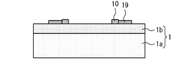
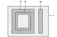
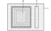
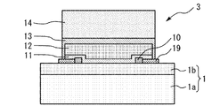
- FIG. 2 It is sectional drawing which shows the manufacturing method of the semiconductor device which concerns on Embodiment 2. It is a top view which shows the manufacturing method of the semiconductor device which concerns on Embodiment 2.
- FIG. 2 It is sectional drawing which shows the manufacturing method of the semiconductor device which concerns on Embodiment 2. It is a top view which shows the manufacturing method of the semiconductor device which concerns on Embodiment 2.
- FIG. 2 It is sectional drawing which shows the manufacturing method of the semiconductor device which concerns on Embodiment 2.
- FIG. 2 It is sectional drawing which shows the manufacturing method of the semiconductor device which concerns on Embodiment 2.
- FIG. 2 It is a top view which shows the manufacturing method of the semiconductor device which concerns on Embodiment 2.
- FIG. 2 It is sectional drawing which shows the manufacturing method of the semiconductor device which concerns on Embodiment 2. It is a top view which shows the manufacturing method of the semiconductor device which concerns on Embodiment 2.
- FIG. It is sectional drawing which shows the manufacturing method of the semiconductor device which concerns on Embodiment 2.
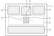
- FIG. 1 is a plan view showing a semiconductor device according to the first embodiment.
- the active region 2 of the transistor is formed on the semiconductor substrate 1.
- a transistor having a plurality of source electrodes 3, gate electrodes 4, and drain electrodes 5 is formed.
- a source pad 6, a gate pad 7, and a drain pad 8 are provided on the semiconductor substrate 1.
- the source pad 6 is connected to a plurality of source electrodes 3.
- the gate pad 7 is connected to the gate electrode 4.
- the drain pad 8 is connected to a plurality of drain electrodes 5.
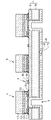
- FIG. 2 is a cross-sectional view of the source pad portion of FIG. In FIG. 2, the insulating film of the electrode, the gate electrode, the drain electrode, and the like are not shown.
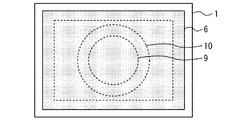
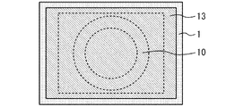
- FIG. 3 is an enlarged plan view of the source pad portion of FIG. 1.
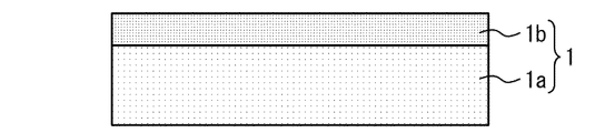
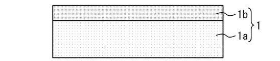
- the semiconductor substrate 1 has a SiC substrate 1a and a GaN layer 1b formed on the SiC substrate 1a.
- the through hole 9 penetrates from the back surface to the front surface of the semiconductor substrate 1.
- the metal film 10 is formed in a ring shape on the surface of the semiconductor substrate 1 so as to surround the through hole 9.
- the metal film 10 is a single-layer metal made of any of Pt, Ni, and Ta, or a multi-layer metal having the metal as the lowermost layer.
- the source pad 6 is formed on the surface of the semiconductor substrate 1.
- the source pad 6 has wiring electrodes 11 and 12, which are sequentially laminated, a surface feeding layer 13, and a surface plating 14.
- the wiring electrodes 11 and 12 cover the through hole 9 and the metal film 10.
- the wiring electrode 11 is bonded to the surface of the semiconductor substrate 1 on the outside of the metal film 10. Since the wiring electrode 11 is in contact with the GaN layer 1b, it is preferably a metal such as Ti.
- the forming range of the wiring electrodes 11 and 12 is smaller than that of the surface feeding layer 13 and the surface plating 14, and larger than that of the metal film 10.
- the back surface electrode 15 is formed on the back surface of the semiconductor substrate 1 and inside the through hole 9, and is directly in contact with and connected to the wiring electrodes 11 and 12.
- the back surface electrode 15 has a back surface feeding layer 16 and a back surface plating 17 laminated in this order.
- the front surface plating 14 and the back surface plating 17 are, for example, Au plating.
- the metal film 10 has a lower ionization tendency and a higher work function than the wiring electrodes 11 and 12. Therefore, Pt is most preferable as the material of the metal film 10, but other metals such as Ni or Ta can be used instead.
- FIGS. 6, 8, 10 and 12 are plan views showing a method of manufacturing a semiconductor device according to the first embodiment. Details of the electrode forming method, thinning of the plate, etc. will be omitted.
- the GaN layer 1b is epitaxially grown on the SiC substrate 1a to form the semiconductor substrate 1.
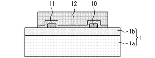
- a metal film 10 is formed in a ring shape on the surface of the semiconductor substrate 1. Since the metal film 10 is patterned in a ring shape by lift-off, for example, a highly anisotropic sputtering method, for example, a long slow sputtering method, is preferable as a film forming method for the metal film 10. Alternatively, the metal film 10 can be formed in a ring shape by performing lift-off using a two-layer resist. From the viewpoint of adhesion, the thickness of the metal film 10 is preferably about several nm to several tens of nm.
- the wiring electrodes 11 and 12 are formed on the surface of the semiconductor substrate 1 so as to cover the metal film 10 having low adhesion to the GaN layer 1b.
- the wiring electrode 11 is bonded to the surface of the semiconductor substrate 1 on the outside of the metal film 10.
- the wiring electrode 12 is used as a receiving metal during dry etching to form a through hole 9, and generally a metal that alloys with Ti to form a stable metal is preferable. Therefore, the material of the wiring electrode 12 is preferably Au or the like, but it may be a single-layer metal or a multi-layer metal. However, if the wiring electrode 12 contains the material of the metal film 10 such as Pt, a residue that is difficult to remove when the through hole 9 is formed is generated. Therefore, it is preferable that the wiring electrode 12 does not contain the material of the metal film 10.
- the surface feeding layer 13 is formed so as to completely cover the wiring electrode 12.
- the material of the surface feeding layer 13 is preferably an alloy using Pt, for example, Ti / Pt / Au or the like.
- Au plating is performed to form the surface plating 14 on the surface feeding layer 13.
- the wafer process on the front side is completed.
- a metal mask 18 such as Ni having an opening at the through hole forming portion is formed.
- the SiC substrate 1a and the GaN layer 1b are sequentially etched from the back surface of the semiconductor substrate 1 by selective dry etching using a fluorine-based gas to form a through hole 9.
- the through hole 9 reaches the wiring electrodes 11 and 12 inside the ring-shaped metal film 10.
- the wiring electrode 11 on the bottom surface of the through hole 9 disappears by dry etching, and etching is stopped at the wiring electrode 12 that functions as a receiving metal.
- Residue is generated on the side wall of the through hole 9 during dry etching. Therefore, wet etching with a strongly acidic solution such as concentrated hydrochloric acid is performed to remove the residue.
- the wiring electrode 11 made of Ti has low wet resistance to a strongly acidic solution. Without the metal film 10, side etching proceeds from the side wall of the bottom surface of the through hole 9, so that an abnormality such as metal floating of the source pad 6 occurs, and reliability including moisture resistance deteriorates. Side etching can be suppressed by providing the metal film 10.
- a back surface feeding layer 16 made of, for example, Ti / Au or the like is formed in the back surface of the semiconductor substrate 1 and the through hole 9 and connected to the wiring electrodes 11 and 12.
- Au plating is performed to form the back surface plating 17 on the back surface feeding layer 16.
- the back surface plating 17 is not limited to Au and may be Cu or the like.
- the metal film 10 is formed on the surface of the semiconductor substrate 1 so as to surround the through hole 9. Since the metal film 10 has a lower ionization tendency than the source pad 6, it has high wet resistance to a strongly acidic solution. Therefore, the side etching of the source pad 6 can be suppressed in the wet etching for removing the side wall residue after the formation of the through hole 9. Further, the source pad 6 is bonded to the surface of the semiconductor substrate 1 on the outside of the metal film 10 having low adhesion. As a result, it is possible to prevent abnormalities such as metal floating of the source pad 6 and improve reliability.
- the metal film 10 when the metal film 10 is formed not in the ring shape but in the entire formed region of the through hole 9, the metal film 10 becomes the receiving metal for dry etching.
- a residue containing Pt that cannot be removed by strong hydrochloric acid treatment is generated on the bottom surface of the through hole 9, which poses a problem in terms of reliability and appearance.
- a metal film 10 which is a high stress metal such as Pt in as small a range as possible, deterioration of adhesion can be suppressed.
- the metal film 10 has a higher work function than the source pad 6. Therefore, since the material of the metal film 10 can also be used for the gate electrode 4 which is Schottky-bonded to the surface of the semiconductor substrate 1, the metal film 10 can be formed at the same time as the gate electrode 4 of the transistor. Therefore, since it is not necessary to add a new process for forming the metal film 10, it is possible to prevent an increase in the number of processes and the product cost.
- the gate electrode 4 includes a film made of the same material as the metal film 10.
- the wiring electrodes 11 and 12 in contact with the back surface electrode 15 formed in the through hole 9 is dry-etched when the through hole 9 is formed. It is preferable that the wiring electrodes 11 and 12 do not contain Pt in order to prevent the generation of a residue containing Pt.
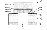
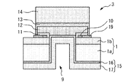
- FIG. 14 is a cross-sectional view showing the semiconductor device according to the second embodiment. This figure is an enlargement of the transistor in the active layer region.
- a source electrode 3, a gate electrode 4, and a drain electrode 5 are formed on the surface of the semiconductor substrate 1.
- the through hole 9 is not formed in the source pad 6 as in the first embodiment, but the through hole 9 is formed in each source electrode 3 in the active region 2. That is, the source electrode 3 is an ISV (individual source via) type source electrode.
- the back surface electrode 15 is connected to the source electrode 3 via the through hole 9.
- the source electrode 3 further has an ohmic electrode 19 that is ohmic-bonded to the surface of the semiconductor substrate 1 outside the metal film 10.
- the gate electrode 4 has a gate base metal 4a that is Schottky-bonded to the surface of the semiconductor substrate 1 and a gate upper metal 4b formed on the gate base metal 4a.
- the semiconductor substrate 1 is formed by epitaxially growing the GaN layer 1b on the SiC substrate 1a.
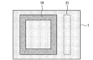
- FIG. 16 shows a source electrode forming region 20 for forming an ISV type source electrode 3 and a gate electrode forming region 21 for forming a gate electrode 4 in a later step.
- an ohmic electrode 19 that is ohmic-bonded to the surface of the semiconductor substrate 1 is formed in the outer peripheral portion of the source electrode forming region 20.
- the ohmic electrode 19 is a single or a combination of metals such as Cu, Ti, Al, Au, Ni, Nb, Pd, Pt, Cr, W, Ta, and Mo.
- the ohmic electrode 19 is ohmic-bonded to the semiconductor substrate 1.
- the ohmic contact of the metal / semiconductor interface can be formed by forming multiple elements including non-metal elements on the semiconductor substrate by vapor deposition or the like and performing heat treatment such as annealing. After the heat treatment, a modified layer containing a plurality of elements is formed at the metal / semiconductor interface.
- a method of adding impurities to epitaxial growth, a method of diffusing impurities by ion implantation and thermal diffusion, or a method of combining a plurality of the above methods can be used.
- a metal film 10 is formed in a ring shape on the surface of the semiconductor substrate 1 inside the ohmic electrode 19.
- the material of the metal film 10 is the same as that of the first embodiment, and Pt metal is used here.
- the metal film 10 is also formed in the gate electrode forming region 21 and used as the gate base metal 4a of the gate electrode 4.
- the gate base metal 4a of the gate electrode 4 is formed at the same time as the metal film 10 in this way, it is possible to avoid an increase in the number of steps.
- the metal film 10 is flush with or overlaps with the ohmic electrode 19.
- the drain electrode 5 does not have to have the same shape as the ISV type source electrode 3 of the present embodiment.
- the wiring electrodes 11 and 12 are formed so as to cover the metal film 10 having low adhesion to the GaN layer 1b.
- the wiring electrode 11 is preferably a metal having high adhesion such as Ti. Further, the wiring electrodes 11 and 12 are formed internally with respect to the ohmic electrode 19 forming the ohmic contact.
- the gate electrode 4 is formed by forming the gate upper metal 4b on the metal film 10 of the gate electrode forming region 21.
- the gate electrode 4 may be a single layer of the metal film 10. In the case of a single layer, it is necessary to increase the film thickness of the metal film 10 because a gate cross section that can withstand the current capacity applied to one gate electrode 4 is required.
- the wiring electrode 12 is preferably a metal containing Au, but a metal such as Cu, Ti, Al, Au, Ni, Nb, Pd, Pt, Cr, W, Ta, and Mo may be used alone or in combination of two or more. However, if the wiring electrode 12 contains the material of the metal film 10 such as Pt, a residue that is difficult to remove when the through hole 9 is formed is generated. Therefore, it is preferable that the wiring electrode 12 does not contain the material of the metal film 10.
- the surface feeding layer 13 is formed so as to completely cover the wiring electrode 12.
- the surface feeding layer 13 is formed so as to be internally reserved for the ohmic electrode 19 and externally reserved for the wiring electrodes 11 and 12.
- the material of the surface feeding layer 13 is preferably an alloy using Pt, for example, Ti / Pt / Au or the like. Thereby, Br corrosion can be suppressed.
- Au plating is performed to form the surface plating 14 on the surface feeding layer 13.
- the wafer process on the front side is completed.
- the metal mask 18 is formed in the same manner as in the first embodiment, and the through holes 9 are formed by selective dry etching or the like.
- the through hole 9 is formed inside the ring-shaped metal film 10 in a plan view. Wet etching is performed to remove the side wall residue generated on the side wall of the through hole 9 during dry etching. By providing the metal film 10, side etching can be suppressed to prevent abnormalities such as metal floating, and reliability can be improved.
- the metal mask 18 is removed, and the back surface feeding layer 16 and the back surface plating 17 are formed in the back surface of the semiconductor substrate 1 and the through hole 9.
- the source electrode 3 is an ISV type source electrode and has the same configuration as the source pad 6 of the first embodiment. Therefore, the same effect as that of the first embodiment can be obtained.
- the metal film 10 made of Pt or the like having a high work function is characteristically undesirable as an ohmic electrode. Therefore, the ohmic electrode 19 is provided on the outer peripheral portion of the lower surface of the source electrode 3 without providing the metal film 10. As a result, deterioration of contact resistance can be suppressed.
Landscapes
- Junction Field-Effect Transistors (AREA)
- Internal Circuitry In Semiconductor Integrated Circuit Devices (AREA)
- Electrodes Of Semiconductors (AREA)
- Engineering & Computer Science (AREA)
- Manufacturing & Machinery (AREA)
Abstract
Description
図1は、実施の形態1に係る半導体装置を示す平面図である。半導体基板1にトランジスタの能動領域2が形成されている。能動領域2には、ソース電極3、ゲート電極4、ドレイン電極5がそれぞれ複数有するトランジスタが形成されている。半導体基板1の上にソースパッド6、ゲートパッド7、ドレインパッド8が設けられている。ソースパッド6は複数のソース電極3に接続されている。ゲートパッド7はゲート電極4に接続されている。ドレインパッド8は複数のドレイン電極5に接続されている。
図14は、実施の形態2に係る半導体装置を示す断面図である。この図は能動層領域のトランジスタを拡大したものである。半導体基板1の表面にソース電極3、ゲート電極4、ドレイン電極5が形成されている。実施の形態1のように貫通孔9をソースパッド6に形成するのではなく、能動領域2内の各ソース電極3に貫通孔9を形成している。即ち、ソース電極3はISV(individual source via)型ソース電極である。裏面電極15が貫通孔9を介してソース電極3に接続されている。ソース電極3は、実施の形態1のソースパッド6の構成に加えて、金属膜10よりも外側で半導体基板1の表面にオーミック接合するオーミック電極19を更に有する。ゲート電極4は、半導体基板1の表面にショットキー接合したゲート下地金属4aと、その上に形成されたゲート上地金属4bとを有する。
Claims (10)
- 互いに対向する表面及び裏面と、前記裏面から前記表面まで貫通する貫通孔とを有する半導体基板と、
前記貫通孔を囲むように前記表面にリング状に形成された金属膜と、
前記貫通孔及び前記金属膜を覆う配線電極を有し、前記金属膜の外側で前記表面に接合された表面電極と、
前記裏面及び前記貫通孔に形成され、前記配線電極に接続された裏面電極とを備え、
前記金属膜は、前記配線電極よりもイオン化傾向が低く仕事関数が高いことを特徴とする半導体装置。 - 前記金属膜は、Pt、Ni、Taの何れかの金属からなる単層金属、又は前記金属を最下層にした複層金属であることを特徴とする請求項1に記載の半導体装置。
- 前記表面にショットキー接合され、前記金属膜と同じ材質の膜を含むゲート電極を更に備えることを特徴とする請求項1又は2に記載の半導体装置。
- 前記配線電極はPtを含まないことを特徴とする請求項1~3の何れか1項に記載の半導体装置。
- 前記表面電極は、前記配線電極の上に形成された表面給電層と、前記表面給電層の上に形成された表面メッキとを有し、
前記表面給電層はPtを含むことを特徴とする請求項1~4の何れか1項に記載の半導体装置。 - 前記表面電極は、トランジスタの複数のソース電極に接続されたソースパッドであることを特徴とする請求項1~5の何れか1項に記載の半導体装置。
- 前記表面電極は、トランジスタのソース電極であり、前記表面にオーミック接合したオーミック電極を有することを特徴とする請求項1~5の何れか1項に記載の半導体装置。
- 半導体基板の表面に金属膜をリング状に形成する工程と、
前記金属膜を覆う配線電極を有する表面電極を前記表面に形成し、前記金属膜の外側で前記表面に接合させる工程と、
前記半導体基板を裏面からエッチングして、リング状の前記金属膜の内側において前記配線電極に達する貫通孔を前記半導体基板に形成する工程と、
前記貫通孔を形成した後に、強酸性溶液を用いたウェットエッチングを実施して、前記貫通孔の側壁に発生した残渣物を除去する工程と、
裏面電極を前記裏面及び前記貫通孔に形成し前記配線電極に接続させる工程とを備え、
前記金属膜は、前記配線電極よりもイオン化傾向が低く仕事関数が高いことを特徴とする半導体装置の製造方法。 - 前記表面にショットキー接合されたゲート電極を前記金属膜と同時に形成する工程を更に備えることを特徴とする請求項8に記載の半導体装置の製造方法。
- 前記金属膜をスパッタ法で形成することを特徴とする請求項8又は9に記載の半導体装置の製造方法。
Priority Applications (6)
| Application Number | Priority Date | Filing Date | Title |
|---|---|---|---|
| JP2022570825A JP7459973B2 (ja) | 2020-12-22 | 2020-12-22 | 半導体装置及びその製造方法 |
| KR1020237019557A KR102761384B1 (ko) | 2020-12-22 | 2020-12-22 | 반도체 장치 및 그 제조 방법 |
| US18/002,642 US12382697B2 (en) | 2020-12-22 | 2020-12-22 | Semiconductor device and method for manufacturing the same |
| DE112020007877.9T DE112020007877T5 (de) | 2020-12-22 | 2020-12-22 | Halbleitervorrichtung und Verfahren zur deren Herstellung |
| CN202080107905.2A CN116569313B (zh) | 2020-12-22 | 2020-12-22 | 半导体装置及其制造方法 |
| PCT/JP2020/047948 WO2022137347A1 (ja) | 2020-12-22 | 2020-12-22 | 半導体装置及びその製造方法 |
Applications Claiming Priority (1)
| Application Number | Priority Date | Filing Date | Title |
|---|---|---|---|
| PCT/JP2020/047948 WO2022137347A1 (ja) | 2020-12-22 | 2020-12-22 | 半導体装置及びその製造方法 |
Publications (1)
| Publication Number | Publication Date |
|---|---|
| WO2022137347A1 true WO2022137347A1 (ja) | 2022-06-30 |
Family
ID=82159209
Family Applications (1)
| Application Number | Title | Priority Date | Filing Date |
|---|---|---|---|
| PCT/JP2020/047948 Ceased WO2022137347A1 (ja) | 2020-12-22 | 2020-12-22 | 半導体装置及びその製造方法 |
Country Status (6)
| Country | Link |
|---|---|
| US (1) | US12382697B2 (ja) |
| JP (1) | JP7459973B2 (ja) |
| KR (1) | KR102761384B1 (ja) |
| CN (1) | CN116569313B (ja) |
| DE (1) | DE112020007877T5 (ja) |
| WO (1) | WO2022137347A1 (ja) |
Cited By (1)
| Publication number | Priority date | Publication date | Assignee | Title |
|---|---|---|---|---|
| WO2025109755A1 (ja) * | 2023-11-24 | 2025-05-30 | 三菱電機株式会社 | 半導体装置およびその製造方法 |
Citations (3)
| Publication number | Priority date | Publication date | Assignee | Title |
|---|---|---|---|---|
| JPH03163835A (ja) * | 1989-11-21 | 1991-07-15 | Nec Corp | バイアホール電極構造 |
| JP2013243173A (ja) * | 2012-05-17 | 2013-12-05 | Sumitomo Electric Ind Ltd | 半導体装置の製造方法 |
| WO2019150526A1 (ja) * | 2018-02-01 | 2019-08-08 | 三菱電機株式会社 | 半導体装置およびその製造方法 |
Family Cites Families (7)
| Publication number | Priority date | Publication date | Assignee | Title |
|---|---|---|---|---|
| JP4322508B2 (ja) * | 2003-01-15 | 2009-09-02 | 新光電気工業株式会社 | 半導体装置の製造方法 |
| JP2006073787A (ja) * | 2004-09-02 | 2006-03-16 | Matsushita Electric Ind Co Ltd | 半導体素子及びその製造方法 |
| JP5021992B2 (ja) * | 2005-09-29 | 2012-09-12 | ルネサスエレクトロニクス株式会社 | 半導体装置およびその製造方法 |
| US8003525B2 (en) * | 2007-06-29 | 2011-08-23 | Fujitsu Limited | Semiconductor device and method of manufacturing the same |
| JP6026756B2 (ja) | 2012-03-06 | 2016-11-16 | 日本電信電話株式会社 | 半導体装置の製造方法 |
| JP5970736B2 (ja) * | 2012-04-27 | 2016-08-17 | 住友電工デバイス・イノベーション株式会社 | 半導体装置の製造方法 |
| JP6034747B2 (ja) | 2013-02-21 | 2016-11-30 | 株式会社東芝 | 半導体装置およびその製造方法 |
-
2020
- 2020-12-22 WO PCT/JP2020/047948 patent/WO2022137347A1/ja not_active Ceased
- 2020-12-22 US US18/002,642 patent/US12382697B2/en active Active
- 2020-12-22 CN CN202080107905.2A patent/CN116569313B/zh active Active
- 2020-12-22 KR KR1020237019557A patent/KR102761384B1/ko active Active
- 2020-12-22 JP JP2022570825A patent/JP7459973B2/ja active Active
- 2020-12-22 DE DE112020007877.9T patent/DE112020007877T5/de active Pending
Patent Citations (3)
| Publication number | Priority date | Publication date | Assignee | Title |
|---|---|---|---|---|
| JPH03163835A (ja) * | 1989-11-21 | 1991-07-15 | Nec Corp | バイアホール電極構造 |
| JP2013243173A (ja) * | 2012-05-17 | 2013-12-05 | Sumitomo Electric Ind Ltd | 半導体装置の製造方法 |
| WO2019150526A1 (ja) * | 2018-02-01 | 2019-08-08 | 三菱電機株式会社 | 半導体装置およびその製造方法 |
Cited By (1)
| Publication number | Priority date | Publication date | Assignee | Title |
|---|---|---|---|---|
| WO2025109755A1 (ja) * | 2023-11-24 | 2025-05-30 | 三菱電機株式会社 | 半導体装置およびその製造方法 |
Also Published As
| Publication number | Publication date |
|---|---|
| US12382697B2 (en) | 2025-08-05 |
| CN116569313A (zh) | 2023-08-08 |
| CN116569313B (zh) | 2025-04-18 |
| JPWO2022137347A1 (ja) | 2022-06-30 |
| DE112020007877T5 (de) | 2023-10-19 |
| US20230238438A1 (en) | 2023-07-27 |
| KR102761384B1 (ko) | 2025-01-31 |
| JP7459973B2 (ja) | 2024-04-02 |
| KR20230101901A (ko) | 2023-07-06 |
Similar Documents
| Publication | Publication Date | Title |
|---|---|---|
| JP7035223B2 (ja) | Iii-v族電界効果トランジスタのゲート構造を形成する方法 | |
| CN111656498B (zh) | 半导体装置及其制造方法 | |
| JP7070848B2 (ja) | 半導体装置の製造方法 | |
| JP2020508573A (ja) | 金フリーコンタクトを有する窒化物構造及びそのような構造を形成する方法 | |
| JP6874928B2 (ja) | 半導体装置 | |
| JP2013232513A (ja) | 半導体装置の製造方法 | |
| JP7215800B2 (ja) | 半導体装置の製造方法および半導体装置 | |
| JP7155482B2 (ja) | 半導体装置 | |
| JP2010092895A (ja) | 半導体装置及びその製造方法 | |
| JP2017228583A (ja) | 半導体装置の製造方法 | |
| JP2008098581A (ja) | 半導体装置及びその製造方法 | |
| JP7459973B2 (ja) | 半導体装置及びその製造方法 | |
| US9640429B2 (en) | Method of fabricating semiconductor device | |
| JP2003045965A (ja) | 半導体装置及び製造方法 | |
| TW201143087A (en) | Compound semiconductor device and method for manufacturing compound semiconductor device | |
| JP2012164711A (ja) | 半導体装置及びその製造方法 | |
| JP2008147294A (ja) | 電子デバイス | |
| WO2025109755A1 (ja) | 半導体装置およびその製造方法 | |
| TW201316466A (zh) | 半導體裝置及其製造方法 | |
| CN115938938A (zh) | 半导体装置的制造方法 | |
| JP2026043975A (ja) | 半導体装置 | |
| JP2019179857A (ja) | 半導体装置および半導体装置の製造方法 | |
| JP2006073787A (ja) | 半導体素子及びその製造方法 | |
| JP5207350B2 (ja) | 窒化物系半導体装置用多層電極構造 | |
| JP2024091550A (ja) | 半導体装置および半導体装置の製造方法 |
Legal Events
| Date | Code | Title | Description |
|---|---|---|---|
| 121 | Ep: the epo has been informed by wipo that ep was designated in this application |
Ref document number: 20966839 Country of ref document: EP Kind code of ref document: A1 |
|
| ENP | Entry into the national phase |
Ref document number: 2022570825 Country of ref document: JP Kind code of ref document: A |
|
| ENP | Entry into the national phase |
Ref document number: 20237019557 Country of ref document: KR Kind code of ref document: A |
|
| WWE | Wipo information: entry into national phase |
Ref document number: 202080107905.2 Country of ref document: CN |
|
| WWE | Wipo information: entry into national phase |
Ref document number: 112020007877 Country of ref document: DE |
|
| 122 | Ep: pct application non-entry in european phase |
Ref document number: 20966839 Country of ref document: EP Kind code of ref document: A1 |
|
| WWG | Wipo information: grant in national office |
Ref document number: 202080107905.2 Country of ref document: CN |
|
| WWG | Wipo information: grant in national office |
Ref document number: 18002642 Country of ref document: US |