WO2022130889A1 - 半導体装置 - Google Patents
半導体装置 Download PDFInfo
- Publication number
- WO2022130889A1 WO2022130889A1 PCT/JP2021/042420 JP2021042420W WO2022130889A1 WO 2022130889 A1 WO2022130889 A1 WO 2022130889A1 JP 2021042420 W JP2021042420 W JP 2021042420W WO 2022130889 A1 WO2022130889 A1 WO 2022130889A1
- Authority
- WO
- WIPO (PCT)
- Prior art keywords
- electrode
- semiconductor device
- semiconductor element
- lead
- connecting member
- Prior art date
- Legal status (The legal status is an assumption and is not a legal conclusion. Google has not performed a legal analysis and makes no representation as to the accuracy of the status listed.)
- Ceased
Links
Images








Classifications
-
- H—ELECTRICITY
- H10—SEMICONDUCTOR DEVICES; ELECTRIC SOLID-STATE DEVICES NOT OTHERWISE PROVIDED FOR
- H10W—GENERIC PACKAGES, INTERCONNECTIONS, CONNECTORS OR OTHER CONSTRUCTIONAL DETAILS OF DEVICES COVERED BY CLASS H10
- H10W90/00—Package configurations
-
- H—ELECTRICITY
- H10—SEMICONDUCTOR DEVICES; ELECTRIC SOLID-STATE DEVICES NOT OTHERWISE PROVIDED FOR
- H10W—GENERIC PACKAGES, INTERCONNECTIONS, CONNECTORS OR OTHER CONSTRUCTIONAL DETAILS OF DEVICES COVERED BY CLASS H10
- H10W70/00—Package substrates; Interposers; Redistribution layers [RDL]
- H10W70/40—Leadframes
- H10W70/421—Shapes or dispositions
- H10W70/442—Shapes or dispositions of multiple leadframes in a single chip
-
- H—ELECTRICITY
- H10—SEMICONDUCTOR DEVICES; ELECTRIC SOLID-STATE DEVICES NOT OTHERWISE PROVIDED FOR
- H10W—GENERIC PACKAGES, INTERCONNECTIONS, CONNECTORS OR OTHER CONSTRUCTIONAL DETAILS OF DEVICES COVERED BY CLASS H10
- H10W70/00—Package substrates; Interposers; Redistribution layers [RDL]
- H10W70/40—Leadframes
- H10W70/464—Additional interconnections in combination with leadframes
- H10W70/466—Tape carriers or flat leads
-
- H—ELECTRICITY
- H10—SEMICONDUCTOR DEVICES; ELECTRIC SOLID-STATE DEVICES NOT OTHERWISE PROVIDED FOR
- H10W—GENERIC PACKAGES, INTERCONNECTIONS, CONNECTORS OR OTHER CONSTRUCTIONAL DETAILS OF DEVICES COVERED BY CLASS H10
- H10W70/00—Package substrates; Interposers; Redistribution layers [RDL]
- H10W70/40—Leadframes
- H10W70/464—Additional interconnections in combination with leadframes
- H10W70/468—Circuit boards
-
- H—ELECTRICITY
- H10—SEMICONDUCTOR DEVICES; ELECTRIC SOLID-STATE DEVICES NOT OTHERWISE PROVIDED FOR
- H10W—GENERIC PACKAGES, INTERCONNECTIONS, CONNECTORS OR OTHER CONSTRUCTIONAL DETAILS OF DEVICES COVERED BY CLASS H10
- H10W70/00—Package substrates; Interposers; Redistribution layers [RDL]
- H10W70/40—Leadframes
- H10W70/481—Leadframes for devices being provided for in groups H10D8/00 - H10D48/00
-
- H—ELECTRICITY
- H10—SEMICONDUCTOR DEVICES; ELECTRIC SOLID-STATE DEVICES NOT OTHERWISE PROVIDED FOR
- H10W—GENERIC PACKAGES, INTERCONNECTIONS, CONNECTORS OR OTHER CONSTRUCTIONAL DETAILS OF DEVICES COVERED BY CLASS H10
- H10W70/00—Package substrates; Interposers; Redistribution layers [RDL]
- H10W70/60—Insulating or insulated package substrates; Interposers; Redistribution layers
- H10W70/62—Insulating or insulated package substrates; Interposers; Redistribution layers characterised by their interconnections
- H10W70/65—Shapes or dispositions of interconnections
-
- H—ELECTRICITY
- H10—SEMICONDUCTOR DEVICES; ELECTRIC SOLID-STATE DEVICES NOT OTHERWISE PROVIDED FOR
- H10W—GENERIC PACKAGES, INTERCONNECTIONS, CONNECTORS OR OTHER CONSTRUCTIONAL DETAILS OF DEVICES COVERED BY CLASS H10
- H10W90/00—Package configurations
- H10W90/811—Multiple chips on leadframes
-
- H—ELECTRICITY
- H10—SEMICONDUCTOR DEVICES; ELECTRIC SOLID-STATE DEVICES NOT OTHERWISE PROVIDED FOR
- H10W—GENERIC PACKAGES, INTERCONNECTIONS, CONNECTORS OR OTHER CONSTRUCTIONAL DETAILS OF DEVICES COVERED BY CLASS H10
- H10W72/00—Interconnections or connectors in packages
- H10W72/50—Bond wires
- H10W72/531—Shapes of wire connectors
- H10W72/5363—Shapes of wire connectors the connected ends being wedge-shaped
-
- H—ELECTRICITY
- H10—SEMICONDUCTOR DEVICES; ELECTRIC SOLID-STATE DEVICES NOT OTHERWISE PROVIDED FOR
- H10W—GENERIC PACKAGES, INTERCONNECTIONS, CONNECTORS OR OTHER CONSTRUCTIONAL DETAILS OF DEVICES COVERED BY CLASS H10
- H10W72/00—Interconnections or connectors in packages
- H10W72/851—Dispositions of multiple connectors or interconnections
- H10W72/853—On the same surface
- H10W72/871—Bond wires and strap connectors
-
- H—ELECTRICITY
- H10—SEMICONDUCTOR DEVICES; ELECTRIC SOLID-STATE DEVICES NOT OTHERWISE PROVIDED FOR
- H10W—GENERIC PACKAGES, INTERCONNECTIONS, CONNECTORS OR OTHER CONSTRUCTIONAL DETAILS OF DEVICES COVERED BY CLASS H10
- H10W72/00—Interconnections or connectors in packages
- H10W72/90—Bond pads, in general
- H10W72/921—Structures or relative sizes of bond pads
- H10W72/926—Multiple bond pads having different sizes
-
- H—ELECTRICITY
- H10—SEMICONDUCTOR DEVICES; ELECTRIC SOLID-STATE DEVICES NOT OTHERWISE PROVIDED FOR
- H10W—GENERIC PACKAGES, INTERCONNECTIONS, CONNECTORS OR OTHER CONSTRUCTIONAL DETAILS OF DEVICES COVERED BY CLASS H10
- H10W72/00—Interconnections or connectors in packages
- H10W72/90—Bond pads, in general
- H10W72/941—Dispositions of bond pads
- H10W72/944—Dispositions of multiple bond pads
-
- H—ELECTRICITY
- H10—SEMICONDUCTOR DEVICES; ELECTRIC SOLID-STATE DEVICES NOT OTHERWISE PROVIDED FOR
- H10W—GENERIC PACKAGES, INTERCONNECTIONS, CONNECTORS OR OTHER CONSTRUCTIONAL DETAILS OF DEVICES COVERED BY CLASS H10
- H10W74/00—Encapsulations, e.g. protective coatings
-
- H—ELECTRICITY
- H10—SEMICONDUCTOR DEVICES; ELECTRIC SOLID-STATE DEVICES NOT OTHERWISE PROVIDED FOR
- H10W—GENERIC PACKAGES, INTERCONNECTIONS, CONNECTORS OR OTHER CONSTRUCTIONAL DETAILS OF DEVICES COVERED BY CLASS H10
- H10W90/00—Package configurations
- H10W90/701—Package configurations characterised by the relative positions of pads or connectors relative to package parts
- H10W90/751—Package configurations characterised by the relative positions of pads or connectors relative to package parts of bond wires
- H10W90/756—Package configurations characterised by the relative positions of pads or connectors relative to package parts of bond wires between a chip and a stacked lead frame, conducting package substrate or heat sink
-
- H—ELECTRICITY
- H10—SEMICONDUCTOR DEVICES; ELECTRIC SOLID-STATE DEVICES NOT OTHERWISE PROVIDED FOR
- H10W—GENERIC PACKAGES, INTERCONNECTIONS, CONNECTORS OR OTHER CONSTRUCTIONAL DETAILS OF DEVICES COVERED BY CLASS H10
- H10W90/00—Package configurations
- H10W90/701—Package configurations characterised by the relative positions of pads or connectors relative to package parts
- H10W90/761—Package configurations characterised by the relative positions of pads or connectors relative to package parts of strap connectors
- H10W90/766—Package configurations characterised by the relative positions of pads or connectors relative to package parts of strap connectors between a chip and a stacked lead frame, conducting package substrate or heat sink
Definitions
- This disclosure relates to semiconductor devices.
- Patent Document 1 discloses an example of a conventional semiconductor device.
- the semiconductor device described in the document includes a semiconductor device, a chip mount (tab), a metal clip, a wire, and a plurality of leads.
- the semiconductor element is a MOSFET (Metal Oxide Semiconductor Field Effect Transistor).
- the semiconductor device has a drain electrode, a source electrode, and a gate electrode.
- the on / off control between the drain electrode and the source electrode is controlled according to the drive signal input to the gate electrode.
- a source electrode and a gate electrode are formed on the front surface of the semiconductor element, and a drain electrode is formed on the back surface.
- the drain electrode conducts with the chip mounting portion by joining the semiconductor element to the chip mounting portion.
- the chip mount is integrally formed with any of the plurality of leads.
- the source electrode conducts to one of a plurality of leads via a metal clip.
- the gate electrode conducts to one of a plurality of leads via a wire.
- the present disclosure provides a semiconductor device capable of facilitating wiring to a certain electrode (for example, a drive signal input electrode) even when the electrode faces downward. It is an issue of.
- the semiconductor device of the present disclosure has a first electrode, a second electrode, and a third electrode, and on / off control between the first electrode and the second electrode is performed according to a first drive signal input to the third electrode.
- the first semiconductor element to be formed, the first conductive member bonded to the third electrode, and the first connecting member bonded to the first conductive member are provided.
- the first semiconductor element has a first main surface and a first back surface that are separated from each other in the thickness direction of the first semiconductor element.
- the second electrode and the third electrode are formed on the first main surface, and the first electrode is formed on the first back surface.
- the first conductive member has a first joint surface and a second joint surface, each of which faces the same direction as the first back surface in the thickness direction and is separated from each other, and the first joint surface and the second joint surface. It has a concave surface recessed in the thickness direction with respect to the surface.
- the third electrode is bonded to the first bonding surface, and the first connecting member is bonded to the second bonding surface and does not overlap with the first semiconductor element when viewed in the thickness direction. It is considered to be an arrangement.
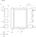
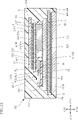
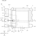
- the semiconductor device A1 includes a first semiconductor element 1, a second semiconductor element 2, a plurality of leads 3, a wiring member 4, a plurality of connecting members 5, and a sealing member 6.
- the plurality of leads 3 include a first lead 31, a second lead 32, a third lead 33, a fourth lead 34, a fifth lead 35, and a sixth lead 36
- the plurality of connecting members 5 include. It includes a first connecting member 51, a second connecting member 52, a third connecting member 53, and a fourth connecting member 54.
- FIG. 1 is a perspective view showing the semiconductor device A1, and the sealing member 6 is shown by an imaginary line (dashed-dotted line).
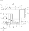
- FIG. 2 is a plan view showing the semiconductor device A1, and the sealing member 6 is shown by an imaginary line.
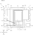
- FIG. 3 is a plan view of FIG. 2 in which the second connecting member 52 is further shown by an imaginary line.
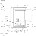
- FIG. 4 is a plan view of FIG. 3 in which the second connecting member 52 is omitted and the first semiconductor element 1 is shown by an imaginary line.
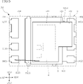
- FIG. 5 is a plan view of FIG. 4, in which the first semiconductor element 1 is omitted and the wiring member 4 is shown by an imaginary line.
- FIG. 6 is a view in which the wiring member 4 is omitted and the third connecting member 53 is shown by an imaginary line in the plan view of FIG.
- FIG. 7 is a plan view of FIG. 6 in which the third connecting member 53 is omitted and the second semiconductor element 2 is shown by an imaginary line.
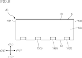
- FIG. 8 is a left side view showing the semiconductor device A1.
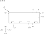
- FIG. 9 is a right side view showing the semiconductor device A1.
- FIG. 10 is a bottom view showing the semiconductor device A1.
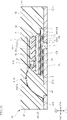
- FIG. 11 is a cross-sectional view taken along the line XI-XI of FIG.
- FIG. 12 is a cross-sectional view taken along the line XII-XII of FIG.
- FIG. 13 is a cross-sectional view taken along the line XIII-XIII of FIG.
- FIG. 14 is a perspective view showing the wiring member 4, and is a diagram showing a part of the wiring member 4 (resin member 43 described later) with an imaginary line.
- the z direction corresponds to, for example, the thickness direction of the semiconductor device A1.
- the first semiconductor element 1 and the second semiconductor element 2 are, for example, MOSFETs, respectively. Instead, the first semiconductor element 1 and the second semiconductor element 2 are field effect transistors including MISFETs (Metal-Insulator-Semiconductor FETs) and HEMTs (High Electron Mobility Transistors), or bipolar transistors such as IGBTs, respectively. It may be.
- Each of the first semiconductor element 1 and the second semiconductor element 2 is made of, for example, SiC (silicon carbide). Instead of this, the first semiconductor element 1 and the second semiconductor element 2 may be composed of Si (silicon), GaAs (gallium arsenide), or GaN (gallium nitride), respectively.
- the first semiconductor element 1 and the second semiconductor element 2 are, for example, rectangular when viewed in the z direction (that is, in a plan view). As shown in FIGS. 3, 6, 12, and 13, the first semiconductor element 1 has a smaller plan view size than the second semiconductor element 2. Further, in a plan view, the entire first semiconductor element 1 overlaps with the second semiconductor element 2.
- the first semiconductor element 1 has a first main surface 101 and a first back surface 102.
- the first main surface 101 and the first back surface 102 are separated from each other in the z direction.
- the first semiconductor element 1 is arranged in such a posture that the first main surface 101 faces the z1 direction and the first back surface 102 faces the z2 direction.
- the first semiconductor element 1 has a first electrode 11, a second electrode 12, and a third electrode 13.
- the first electrode 11 is formed on the first back surface 102, and the second electrode 12 and the third electrode 13 are formed on the first main surface 101.
- the first electrode 11 is a drain electrode
- the second electrode 12 is a source electrode
- the third electrode 13 is a gate electrode.
- a first drive signal for example, a gate voltage
- the third electrode 13 gate electrode
- on / off control is performed between the first electrode 11 (drain electrode) and the second electrode 12 (source electrode). Will be done.
- the first semiconductor element 1 switches between the conduction state and the cutoff state according to the first drive signal.
- the operation of switching between the conduction state and the cutoff state is called a switching operation.
- a current flows from the first electrode 11 (drain electrode) to the second electrode 12 (source electrode), and in the cutoff state, this current does not flow.
- the second semiconductor element 2 has a second main surface 201 and a second back surface 202.
- the second main surface 201 and the second back surface 202 are separated from each other in the z direction.
- the second semiconductor element 2 is arranged in such a posture that the second main surface 201 faces the z1 direction and the second back surface 202 faces the z2 direction.
- the second semiconductor element 2 has a fourth electrode 21, a fifth electrode 22, and a sixth electrode 23.
- the fourth electrode 21 is formed on the second back surface 202, and the fifth electrode 22 and the sixth electrode 23 are formed on the second main surface 201.
- the fourth electrode 21 is a drain electrode
- the fifth electrode 22 is a source electrode
- the sixth electrode 23 is a gate electrode.
- a second drive signal (for example, a gate voltage) is input to the sixth electrode 23 (gate electrode), and on / off control is performed between the fourth electrode 21 (drain electrode) and the fifth electrode 22 (source electrode). Will be done.
- the second semiconductor element 2 switches between the conduction state and the cutoff state according to the second drive signal.
- the second drive signal for example, the gate voltage
- the second semiconductor element 2 switches between the conduction state and the cutoff state according to the second drive signal.
- a current flows from the fourth electrode 21 (drain electrode) to the fifth electrode 22 (source electrode), and in the cutoff state, this current does not flow.
- the semiconductor device A1 converts a DC voltage into, for example, an AC voltage by each switching operation of the first semiconductor element 1 and the second semiconductor element 2.
- the DC voltage is input between the second lead 32 and the third lead 33, and the AC voltage is output from the fifth lead 35.
- Each path of the current generated by the DC voltage and the current generated by the AC voltage is the main current path in the semiconductor device A1.
- the semiconductor device A1 is configured as, for example, a half-bridge type switching circuit.
- the first semiconductor element 1 constitutes the upper arm circuit of the semiconductor device A1
- the second semiconductor element 2 constitutes the lower arm circuit of the semiconductor device A1.
- the first semiconductor element 1 and the second semiconductor element 2 are connected in series to form a bridge.
- the plurality of leads 3 support the first semiconductor element 1 and the second semiconductor element 2, and appropriately conduct to the first semiconductor element 1 and the second semiconductor element 2. As shown in FIGS. 11 to 13, each of the plurality of leads 3 is located on the side opposite to the first semiconductor element 1 (on the z1 direction side) with respect to the second semiconductor element 2 in the z direction.
- the plurality of leads 3 are made of a conductive material and are formed by using, for example, a lead frame.
- the plurality of leads 3 are formed by subjecting a metal plate material such as Cu or a Cu alloy to a cutting process such as punching and a bending process. As shown in FIGS. 8 to 10, the plurality of leads 3 are partially exposed from the sealing member 6, and the exposed portions are used as terminals of the semiconductor device A1.
- the plurality of leads 3 include a first lead 31, a second lead 32, a third lead 33, a fourth lead 34, a fifth lead 35, and a sixth lead 36.
- the first lead 31, the second lead 32, the third lead 33, the fourth lead 34, the fifth lead 35, and the sixth lead 36 are separated from each other.
- the first lead 31 conducts to the third electrode 13 (gate electrode) of the first semiconductor element 1. As shown in FIGS. 8 and 10, a part of the first lead 31 is exposed from the sealing member 6. This exposed portion is a terminal of the semiconductor device A1, and in the semiconductor device A1, the first lead 31 is an input terminal of the first drive signal.
- the second lead 32 conducts to the first electrode 11 (drain electrode) of the first semiconductor element 1. As shown in FIGS. 8 and 10, a part of the second lead 32 is exposed from the sealing member 6. This exposed portion is a terminal of the semiconductor device A1, and in the semiconductor device A1, the second lead 32 is an input terminal (P terminal) on the positive electrode side.
- the third lead 33 conducts to the fifth electrode 22 (source electrode) of the second semiconductor element 2. As shown in FIG. 10, a part of the third lead 33 is exposed from the sealing member 6. This exposed portion is a terminal of the semiconductor device A1, and in the semiconductor device A1, the third lead 33 is an input terminal (N terminal) on the negative electrode side. As shown in FIGS. 11 to 13, in the third lead 33, the fifth electrode 22 of the second semiconductor element 2 is bonded via the conductive bonding material 922, and the second semiconductor element 2 is mounted on the third lead 33. ..
- the conductive bonding material 922 is made of, for example, solder, a metal paste, a sintered metal, or the like, and is appropriately omitted in FIGS. 1 to 7.
- the third lead 33 includes a pad portion 331 and a plurality of suspension portions 332.
- the pad portion 331 is a portion of the third lead 33 to which the fifth electrode 22 of the second semiconductor element 2 is bonded by the conductive bonding material 922.
- Each of the plurality of suspension portions 332 is a portion that supports the pad portion 331 when the plurality of leads 3 are lead frames at the time of manufacturing the semiconductor device A1.
- Each of the plurality of suspension portions 332 has a surface opposite to the portion connected to the pad portion 331 exposed from the sealing member 6 in the y direction.
- the fourth lead 34 conducts to the sixth electrode 23 (gate electrode) of the second semiconductor element 2. As shown in FIGS. 9 and 10, a part of the fourth lead 34 is exposed from the sealing member 6. This exposed portion is a terminal of the semiconductor device A1, and in the semiconductor device A1, the fourth lead 34 is an input terminal of a second drive signal.
- the fourth lead 34 includes the pad portion 341.
- the pad portion 341 is a portion of the fourth lead 34 to which the sixth electrode 23 of the second semiconductor element 2 is joined.
- the sixth electrode 23 is bonded to the pad portion 341 by the conductive bonding material 923.
- the conductive bonding material 923 is made of, for example, solder, a metal paste or a sintered metal.
- the fifth lead 35 conducts to the second electrode 12 (source electrode) of the first semiconductor element 1 and to the fourth electrode 21 (drain electrode) of the second semiconductor element 2. As shown in FIGS. 9 and 10, a part of the fifth lead 35 is exposed from the sealing member 6. This exposed portion is a terminal of the semiconductor device A1, and in the semiconductor device A1, the fifth lead 35 is an AC voltage output terminal.
- the sixth lead 36 conducts to the fourth electrode 21 (drain electrode) of the second semiconductor element 2. As shown in FIGS. 8 and 10, a part of the sixth lead 36 is exposed from the sealing member 6. This exposed portion is a terminal of the semiconductor device A1, and in the semiconductor device A1, the sixth lead 36 is a terminal for detecting an output voltage.
- the third lead 33 is located at the center (or substantially the center) of the semiconductor device A1 in the x direction and is connected in the y direction.
- the first lead 31, the second lead 32, and the sixth lead 36 are located on one side (x1 direction side) of the third lead 33 in the x direction, and the fourth lead 34 and the fifth lead 35 are the third leads. It is located on the other side (x2 direction side) in the x direction from 33.
- the first lead 31, the second lead 32, and the sixth lead 36 are arranged in the y direction, and the first lead 31 is sandwiched between the second lead 32 and the sixth lead 36 in the y direction.
- the second lead 32 is located on one side (y2 direction side) in the y direction with respect to the first lead 31.
- the fourth lead 34 is located on the other side (y1 direction side) in the y direction with respect to the fifth lead 35.
- the sixth lead 36 overlaps the fourth lead 34 when viewed in the x direction, and the first lead 31 and the second lead 32 each overlap the fifth lead 35 when viewed in the x direction.
- the shape and arrangement of each lead 3 (1st lead 31, 2nd lead 32, 3rd lead 33, 4th lead 34, 5th lead 35 and 6th lead 36) is not limited to the illustrated example.
- the wiring member 4 is located between the first semiconductor element 1 and the second semiconductor element 2 in the z direction. As shown in FIGS. 4 and 11 to 14, the wiring member 4 has a first conduction member 41, a second conduction member 42, and a resin member 43.
- the first conductive member 41 is made of a conductive material. This conductive material is, for example, Cu or a Cu alloy. As shown in FIGS. 4 and 11 to 13, the first conductive member 41 has a first joint surface 411, a second joint surface 412, a concave surface 413, and a covering surface 414.
- the first joint surface 411 and the second joint surface 412 face the z2 direction. That is, the first joint surface 411 and the second joint surface 412 face the same direction as the first back surface 102 and the second back surface 202 in the z direction.
- the first junction surface 411 overlaps with the first semiconductor element 1
- the second junction surface 412 does not overlap with the first semiconductor element 1.
- the first joint surface 411 does not overlap with the second connecting member 52 in a plan view.
- the third electrode 13 of the first semiconductor element 1 is bonded to the first bonding surface 411 by the conductive bonding material 913.
- the conductive bonding material 913 is made of, for example, solder, a metal paste or a sintered metal.
- the first connecting member 51 is joined to the second joining surface 412.
- the first joint surface 411 and the second joint surface 412 are located on the same plane orthogonal to the z direction. Further, the first joint surface 411 and the second joint surface 412 are arranged apart from each other along the y direction.
- the concave surface 413 is sandwiched between the first joint surface 411 and the second joint surface 412 in a plan view, with respect to the first joint surface 411 and the second joint surface 412. It dents in the z direction.
- the concave surface 413 is defined by a plurality of planes (eg, a bottom surface and a pair of side surfaces), but may be curved as a whole (eg, one of the above three surfaces). One surface may be curved, or two or three surfaces may be curved respectively).
- a resin member 43 is formed in a portion recessed by the concave surface 413.
- the covering surface 414 is covered with the resin member 43.
- the covering surface 414 faces the z1 direction. That is, the covering surface 414 faces the side opposite to the first joint surface 411 and the second joint surface 412 in the z direction.
- the second conductive member 42 is made of a conductive material.
- the conductive material is Cu or a Cu alloy, similar to, for example, the first conductive member 41.
- the second conductive member 42 is separated from the first conductive member 41 and is insulated from the first conductive member 41.
- the second conductive member 42 is sandwiched between the first semiconductor element 1 and the second semiconductor element 2 in the z direction.
- the second conduction member 42 has a first top surface 421 and a second top surface 422, as shown in FIGS. 12 and 13.
- the first top surface 421 and the second top surface 422 are separated from each other in the z direction.
- the first top surface 421 faces the z1 direction, and the second top surface 422 faces the z2 direction.
- the first top surface 421 is joined to the third connecting member 53 by the conductive joining material 94.
- the conductive bonding material 94 is made of, for example, solder, a metal paste or a sintered metal.
- the second top surface 422 is bonded to the second electrode 12 of the first semiconductor element 1 by the conductive bonding material 912.
- the conductive bonding material 912 is made of, for example, solder, a metal paste, a sintered metal, or the like.
- the second top surface 422 is located on the same plane orthogonal to the first joint surface 411 and the second joint surface 412 in the z direction.
- the resin member 43 partially covers the first conductive member 41 and the second conductive member 42.
- the first joint surface 411 and the second joint surface 412 of the first conductive member 41 and the first top surface 421 and the second top surface 422 of the second conductive member 42 are exposed from the resin member 43. do.
- the resin member 43 is made of, for example, an insulating resin material. This resin material is, for example, an epoxy resin. Instead of this, the constituent material of the resin member 43 may be a glass epoxy resin.
- the plurality of connecting members 5 are electrically connected to each other at two or more portions separated from each other.
- the plurality of connecting members 5 include a first connecting member 51, a second connecting member 52, a third connecting member 53, and a fourth connecting member 54.
- the first connection member 51 conducts the first conduction member 41 and the first lead 31 of the wiring member 4.
- the first connecting member 51 is, for example, a bonding wire. Instead of this, the first connecting member 51 may be a bonding ribbon, a metal plate, or the like.
- the first connecting member 51 is made of, for example, Au or Au alloy, Cu or Cu alloy, or Al or Al alloy. As shown in FIG. 11, one end of the first connecting member 51 is joined to the second joining surface 412 of the first conducting member 41, and the other end is joined to the upper surface of the first lead 31.
- the second connection member 52 conducts the first electrode 11 of the first semiconductor element 1 and the second lead 32.
- the second connecting member 52 is, for example, a metal plate (also referred to as a metal clip).
- the second connecting member 52 is made of, for example, Cu or a Cu alloy.
- the second connecting member 52 serves as a main current path in the semiconductor device A1. Therefore, a metal plate is more suitable for high current and high voltage than a bonding wire.
- the second connecting member 52 includes two joint portions 521, 522 and a connecting portion 523.
- the joining portion 521 is joined onto the first electrode 11 via the conductive joining material 911.
- the conductive bonding material 911 is made of, for example, solder, a metal paste, a sintered metal, or the like.
- the joining portion 522 is joined onto the second lead 32 via the conductive joining material 952.
- the conductive bonding material 952 is made of, for example, solder, a metal paste, a sintered metal, or the like.
- the connecting portion 523 connects to the two joining portions 521 and 522 and connects them. The two joints 521 and 522 conduct with each other via the joint 523.
- the third connection member 53 conducts the second conduction member 42 of the wiring member 4 and the fourth electrode 21 (drain electrode) of the second semiconductor element 2 and conducts these with the fifth lead 35.
- the third connecting member 53 is, for example, a metal plate (also referred to as a metal clip).
- the third connecting member 53 is made of, for example, Cu or a Cu alloy.
- the third connection member 53 serves as a main current path in the semiconductor device A1. Therefore, a metal plate is more suitable for high current and high voltage than a bonding wire.
- the third connecting member 53 includes an intervening portion 531, a joining portion 532, and a connecting portion 533.
- the intervening portion 531 is sandwiched between the second conductive member 42 and the fourth electrode 21 in the z direction, and is conductive to the second conductive member 42 and the fourth electrode 21. ..
- the intervening portion 531 is joined on the fourth electrode 21 by the conductive joining material 921.
- the conductive bonding material 921 is made of, for example, solder, a metal paste or a sintered metal.
- the second conductive member 42 is joined to the intervening portion 531 by the conductive joining material 94.
- one end of the fourth connecting member 54 is joined to a portion of the intervening portion 531 (a part of the third connecting member 53). This joint portion is a portion that does not overlap with any of the first semiconductor element 1, the wiring member 4, and the second connection member 52 in a plan view.
- the joining portion 532 is joined on the fifth lead 35 by the conductive joining material 953.
- the joint portion 532 conducts to the fifth lead 35 via the conductive joint material 953.
- the conductive bonding material 953 is made of, for example, solder, a metal paste, a sintered metal, or the like.
- the connecting portion 533 connects to the intervening portion 531 and the joining portion 532, and connects them.
- the intervening portion 531 and the joint portion 532 are conductive via the connecting portion 533.
- the fourth connecting member 54 conducts the third connecting member 53 and the sixth lead 36.
- the fourth connecting member 54 is, for example, a bonding wire. Instead of this, the fourth connecting member 54 may be a bonding ribbon, a metal plate, or the like.
- the fourth connecting member 54 is made of, for example, Au or Au alloy, Al or Al alloy, or Cu or Cu alloy. One end of the fourth connecting member 54 is joined to the intervening portion 531 of the third connecting member 53, and the other end is joined to the upper surface of the sixth lead 36.
- the sealing member 6 covers the wiring member 4 and the plurality of connecting members 5 by a part of the first semiconductor element 1, the second semiconductor element 2, and the plurality of leads 3.
- the sealing member 6 is made of, for example, an insulating resin material.
- the resin material for example, the same epoxy resin as the resin member 43 is used.
- the sealing member 6 has a resin main surface 61, a resin back surface 62, and a plurality of resin side surfaces 631 to 634.
- the resin main surface 61 and the resin back surface 62 are separated from each other in the z direction as shown in FIGS. 8, 9, and 11 to 13.
- the resin main surface 61 faces the z2 direction
- the resin back surface 62 faces the z1 direction.
- the plurality of resin side surfaces 631 to 634 are sandwiched between the resin main surface 61 and the resin back surface 62 in the z direction, and are connected to the resin main surface 61 and the resin back surface 62, respectively.
- the resin side surface 631 and the resin side surface 632 are separated from each other in the x direction.
- the resin side surface 631 faces the x1 direction
- the resin side surface 632 faces the x2 direction.
- the resin side surface 633 and the resin side surface 634 are separated from each other in the y direction.
- the resin side surface 633 faces the y1 direction, and the resin side surface 634 faces the y2 direction.
- a part of each of the plurality of leads 3 is exposed from the resin back surface 62. Further, a part of each of the first lead 31, the second lead 32 and the third lead 33 is exposed from the resin side surface 631, and a part of each of the fourth lead 34 and the fifth lead 35 is exposed from the resin side surface 632. Be exposed.
- the effects of the semiconductor device A1 are as follows.
- the semiconductor device A1 includes a first semiconductor element 1 and a first conduction member 41.
- the first semiconductor element 1 has a first electrode 11, a second electrode 12, and a third electrode 13, and the first electrode 11 and the second electrode 12 are obtained by a first drive signal input to the third electrode 13. The interval is controlled on and off. That is, the third electrode 13 is an input electrode for the first drive signal.
- the first electrode 11 is formed on the first back surface 102 of the first semiconductor element 1, and the second electrode 12 and the third electrode 13 are formed on the first main surface 101.
- the first conducting member 41 has a first joining surface 411 and a second joining surface 412. The first joint surface 411 and the second joint surface 412 face the first back surface 102 in the same direction.
- the first bonding surface 411 is bonded to the third electrode 13, and the second bonding surface 412 does not overlap with the first semiconductor element 1 in a plan view. According to this configuration, since the second joining surface 412 faces upward of the semiconductor device A1 and does not overlap with the first semiconductor element 1, the first connecting member 51 can be easily joined to the second joining surface 412. Therefore, the semiconductor device A1 can facilitate wiring of the drive signal for on / off control of the first semiconductor element 1 to the input electrode (third electrode 13).
- the semiconductor device A1 includes a first semiconductor element 1 and a second semiconductor element 2.
- the first semiconductor element 1 overlaps with the second semiconductor element 2 in a plan view.
- the third electrode 13 faces the second semiconductor element 2 and is directly connected to the third electrode 13. It becomes more difficult to join the members 51.
- a third connecting member 53 and a third lead 33 are arranged below the first semiconductor element 1 (in the z1 direction), so that the third electrode 13 is reached. It becomes more difficult to join the first connecting member 51 of the above.
- the semiconductor device A1 since the second joining surface 412 faces upward of the semiconductor device A1 by the wiring member 4 (first conducting member 41), the joining of the first connecting member 51 becomes easy. That is, the semiconductor device A1 is more effective in mounting the first semiconductor element 1 and the second semiconductor element 2 in a stack structure, and mounting the first semiconductor element 1 and the second semiconductor element 2 on flip chips, respectively. be.
- the first conduction member 41 includes a concave surface 413 recessed from the first joint surface 411 and the second joint surface 412. According to this configuration, in the first conductive member 41, the first bonding surface 411 is only conductively bonded to the third electrode 13 via the conductive bonding material 913 with respect to the first semiconductor element 1. Therefore, the semiconductor device A1 can suppress unintended conduction between the first conduction member 41 and the first semiconductor element 1. For example, it is possible to suppress unintended conduction between the first electrode 11 formed on the first main surface 101 and the first conduction member 41 as in the third electrode 13.
- the second semiconductor element 2 is flip-chip mounted, and the fifth electrode 22 (source electrode) is bonded to the third lead 33. According to this configuration, it is possible to improve the heat dissipation property of the heat generated by the switching operation of the second semiconductor element 2.
- the second junction surface 412 overlaps the third connecting member 53 (intervening portion 531), the second semiconductor element 2 and the third lead 33 (pad portion 331) in a plan view (see FIG. 13). ..
- the wiring member 4 is supported by the third connecting member 53, the second semiconductor element 2, and the third lead 33, the wiring member 4 is displaced due to the pressing force and the first connecting member 51 is poorly joined. Can be suppressed.
- FIG. 15 shows the semiconductor device A2 according to the second embodiment.
- FIG. 15 is a cross-sectional view showing the semiconductor device A2 and corresponds to the cross section of FIG.
- the semiconductor device A2 differs from the semiconductor device A1 in that a part of the first semiconductor element 1 is covered with the resin member 43.
- the resin member 43 covers the first semiconductor element 1 except for the first back surface 102 of the first semiconductor element 1. That is, the first back surface 102 is exposed from the resin member 43. Since the first electrode 11 of the first semiconductor element 1 is formed on the first back surface 102, the first electrode 11 of the first semiconductor element 1 is exposed from the resin member 43.
- the second junction surface 412 is located above the first junction surface 411 (in the z2 direction) and is the same as the first back surface 102 of the first semiconductor element 1. Located on a plane. As a result, even when the resin member 43 partially covers the first semiconductor element 1, the second joint surface 412 is exposed from the resin member 43.
- the first semiconductor element 1 is integrally formed with the wiring member 4 in advance at the time of manufacturing the semiconductor device A2.
- the first conductive member 41 is bonded to the third electrode 13 of the first semiconductor element 1 and the second conductive member 42 is bonded to the second electrode 12 of the first semiconductor element 1
- the first semiconductor element 1 is covered with the resin member 43.
- the wiring member 4 in which the first semiconductor element 1 is integrated is formed. In this way, the wiring member 4 in which the first semiconductor element 1 is integrated is formed in advance, and the semiconductor device A2 is manufactured.
- the semiconductor device A2 can also have the same effect as the semiconductor device A1.
- FIG. 16 shows the semiconductor device A3 according to the third embodiment.
- FIG. 16 is a cross-sectional view showing the semiconductor device A3 and corresponds to the cross section of FIG.
- the wiring member 4 does not include the second conduction member 42, and the intervening portion 531 of the third connection member 53 has the first portion 531a and the first portion 531a. It differs in that it includes the second part 531b.
- the first part 531a has a larger dimension in the x direction than the second part 531b. That is, the first part 531a is thicker than the second part 531b.
- a second electrode 12 is bonded to the upper surface of the first portion 531a via a conductive bonding material 912.
- the first part 531a is arranged at the same position (or substantially the same) as the second conductive member 42 of the semiconductor device A1 in a plan view.
- a wiring member 4 is joined to the upper surface of the second part 531b via a conductive joining material 94.
- the upper surface of the first portion 531a and the upper surface of the wiring member 4 are arranged at the same (or substantially the same) position in the z direction.
- the semiconductor device A3 can also have the same effect as the semiconductor device A1.
- FIG. 17 shows the semiconductor device A4 according to the fourth embodiment.
- FIG. 17 is a cross-sectional view showing the semiconductor device A4 and corresponds to the cross section of FIG.
- the semiconductor device A4 differs from the semiconductor device A3 in that the wiring member 4 does not include the resin member 43.
- the intervening portion 531 of the third connecting member 53 includes the first portion 531a and the second portion 531b, similarly to the intervening portion 531 of the semiconductor device A2.
- the wiring member 4 is composed of only the first conduction member 41.
- the first conductive member 41 is covered with a sealing member 6. Therefore, the covering surface 414 of the semiconductor device A3 is covered with the sealing member 6.
- the first conduction member 41 is bonded to the third electrode 13 of the first semiconductor element 1 before the first semiconductor element 1 is mounted on the first portion 531a (intervening portion 531). , The first conducting member 41 is supported in a posture separated from the third connecting member 53.
- the semiconductor device A4 can also have the same effect as the semiconductor device A1.
- 18 and 19 show the semiconductor device A5 according to the fifth embodiment.
- 18 and 19 are plan views showing the semiconductor device A5.
- the sealing member 6 is shown by an imaginary line
- the second connecting member 52 is omitted
- the first semiconductor element 1 and the sealing member 6 are shown by an imaginary line.
- the first joint surface 411 and the second joint surface 412 are separated from each other in the x direction as compared with the semiconductor device A1. It differs in that it is arranged.
- the second joint surface 412 is located on one side (x1 direction side) of the first joint surface 411 in the x direction. In this way, the second joint surface 412 is prevented from overlapping the first semiconductor element 1 and the second connecting member 52 in a plan view.
- the semiconductor device A5 can also have the same effect as the semiconductor device A1.
- FIGS. 20 and 21 show the semiconductor device A6 according to the sixth embodiment.
- FIG. 20 is a plan view showing the semiconductor device A6, and the second connecting member 52 and the sealing member 6 are shown by imaginary lines.
- FIG. 21 is a cross-sectional view taken along the line XXI-XXI of FIG.
- the semiconductor device A6 has the same (or omitted) the plan view size of the first semiconductor element 1 and the plan view size of the second semiconductor device 2 as compared with the semiconductor device A5. The same).
- the semiconductor device A6 as in the semiconductor device A5, the first conduction member 41 in which the first joint surface 411 and the second joint surface 412 are arranged along the y direction is used.
- the plan view size of the first semiconductor element 1 and the plan view size of the second semiconductor device 2 are the same (or substantially the same).
- the first semiconductor element 1 is arranged slightly offset in the x2 direction from the second semiconductor element 2.
- the semiconductor device A6 can also have the same effect as the semiconductor device A1.
- the first joint surface 411 and the second joint surface 412 are arranged along the y direction, and in the fifth embodiment and the sixth embodiment, the first joint surface 411 and the second joint surface 411 are arranged.
- FIG. 22 is a plan view showing the semiconductor device according to the modification, and corresponds to FIG. 19.
- the position of the second joint surface 412 is changed in the semiconductor device A5.
- the arrangement of the first joint surface 411 and the second joint surface 412 can be appropriately arranged according to the shape and position of other components. You can change it.
- the second semiconductor element 2 is an example of a transistor, but the present invention is not limited to this, and a diode, an IC, or the like may be used.
- the second semiconductor element 2 in an example in which the second semiconductor element 2 is a diode, the second semiconductor element 2 has two electrodes, one for each of the second main surface 201 and the second back surface 202. They may be provided one by one, or may be provided on either the second main surface 201 or the second back surface 202.
- an electronic component such as a resistor or a capacitor may be provided instead of the second semiconductor element 2.
- each of the semiconductor devices A1 to A6 does not have to include the second semiconductor element 2. In these modifications, the arrangement, shape, and number of the plurality of leads 3 are appropriately changed.
- the semiconductor devices A1 to A6 may include a glass epoxy substrate, a silicon substrate, a ceramic substrate, or the like on which a wiring pattern is formed, instead of the plurality of leads 3.
- the semiconductor device according to the present disclosure is not limited to the above-described embodiment.
- the specific configuration of each part of the semiconductor device of the present disclosure can be freely redesigned.
- the present disclosure includes embodiments described in the appendix below. Appendix 1.
- a first semiconductor device having a first electrode, a second electrode, and a third electrode, and the on / off control between the first electrode and the second electrode is performed according to a first drive signal input to the third electrode.
- the first semiconductor element has a first main surface and a first back surface that are separated from each other in the thickness direction of the first semiconductor element.
- the second electrode and the third electrode are formed on the first main surface.
- the first electrode is formed on the first back surface, and the first electrode is formed on the first back surface.
- the first conductive member has a first joint surface and a second joint surface, each of which faces the same direction as the first back surface in the thickness direction and is separated from each other, and the first joint surface and the second joint surface. It has a concave surface recessed in the thickness direction with respect to the surface, and has a concave surface.
- the third electrode is joined to the first joint surface.
- the second bonding surface is a semiconductor device to which the first connecting member is bonded and does not overlap with the first semiconductor element when viewed in the thickness direction. Appendix 2. Further, a plurality of leads arranged in a direction in which the first main surface faces the first semiconductor element in the thickness direction are further provided.
- the semiconductor device wherein the plurality of leads include a first lead to which the first connecting member is connected. Appendix 3. A second connecting member joined to the first electrode is further provided. The plurality of leads include a second lead to which the second connecting member is joined. The semiconductor device according to Appendix 2, wherein the first electrode and the second lead are conductive via the second connecting member. Appendix 4. Further comprising a second semiconductor device having a second main surface facing the same direction as the first main surface and a second back surface facing the same direction as the first back surface in the thickness direction. The plurality of leads are located on the side opposite to the first semiconductor element with respect to the second semiconductor element in the thickness direction, and include a third lead on which the second semiconductor element is mounted. The semiconductor device described in 1.
- the second semiconductor element has a fourth electrode and a fifth electrode, the fourth electrode is formed on the second back surface, and the fifth electrode is formed on the second main surface.
- the first semiconductor element and the second semiconductor element overlap each other in the thickness direction.
- the semiconductor device according to Appendix 5, wherein the second semiconductor element faces the first main surface.
- the second semiconductor element has a sixth electrode formed on the second main surface, and the fourth electrode and the fifth electrode are turned on and off according to a second drive signal input to the sixth electrode.
- Appendix 9. The semiconductor device according to Appendix 8, wherein the plurality of leads include a fourth lead to which the sixth electrode is bonded.
- Appendix 10. Further, a plate-shaped third connecting member conducting the second electrode and the fourth electrode is provided.
- the plurality of leads include a fifth lead joined to the third connecting member.
- the semiconductor device according to Appendix 9, wherein the second electrode, the fourth electrode, and the fifth lead are conductive via the third connecting member.
- Appendix 11. Further provided with an insulating resin member covering the first conducting member, The first conducting member has a covering surface that faces the first joint surface and the side opposite to the second joint surface in the thickness direction and is covered with the resin member.
- the semiconductor device according to Appendix 10 wherein the second joint surface is exposed from the resin member.
- Appendix 12. A second conductive member sandwiched between the first semiconductor element and the second semiconductor element in the thickness direction and insulated from the first conductive member is further provided.
- Appendix 13 The third connecting member is sandwiched between the second conducting member and the fourth electrode in the thickness direction.
- Appendix 14. The resin member covers the second conductive member, and the resin member covers the second conductive member.
- the second conducting member has a first top surface joined to the third connecting member.
- the semiconductor device according to Appendix 13 wherein the first top surface is exposed from the resin member.
- Appendix 15. The second conducting member has a second top surface joined to the second electrode. The second top surface is exposed from the resin member and is exposed.
- Appendix 16. The resin member covers the first semiconductor element, and the resin member covers the first semiconductor element.
- the semiconductor device according to Appendix 14, wherein the second joint surface and the first back surface are located on the same plane orthogonal to the thickness direction.
- Appendix 17. The semiconductor device according to any one of Supplementary note 12 to Supplementary note 16, further comprising a first semiconductor element, the second semiconductor element, the first conductive member, and a sealing member covering the second conductive member.
- A1 to A6 Semiconductor device 1: 1st semiconductor element 101: 1st main surface 102: 1st back surface 11: 1st electrode 12: 2nd electrode 13: 3rd electrode 2: 2nd semiconductor element 201: 2nd main surface 202: 2nd back surface 21: 4th electrode 22: 5th electrode 23: 6th electrode 3: Lead 31: 1st lead 32: 2nd lead 33: 3rd lead 331: Pad part 332: Suspended part 34: 4th Lead 341: Pad 35: 5th lead 36: 6th lead 4: Wiring member 41: 1st conduction member 411: 1st joint surface 412: 2nd joint surface 413: Concave surface 414: Covered surface 42: 2nd conduction member 421: First top surface 422: Second top surface 43: Resin member 5: Connection member 51: First connection member 52: Second connection member 521: Joint part 522: Joint part 523: Connection part 53: Third connection member 531: Intervening part 531a: First part 531b: Second
Landscapes
- Lead Frames For Integrated Circuits (AREA)
- Structures Or Materials For Encapsulating Or Coating Semiconductor Devices Or Solid State Devices (AREA)
- Physics & Mathematics (AREA)
- Geometry (AREA)
- Wire Bonding (AREA)
Abstract
Description
付記1.
第1電極、第2電極および第3電極を有し、前記第3電極に入力される第1駆動信号に応じて前記第1電極および前記第2電極間がオンオフ制御される第1半導体素子と、
前記第3電極に接合された第1導通部材と、
前記第1導通部材に接合された第1接続部材と、
を備えており、
前記第1半導体素子は、前記第1半導体素子の厚さ方向に離間する第1主面および第1裏面を有し、
前記第1主面には、前記第2電極および前記第3電極が形成され、
前記第1裏面には、前記第1電極が形成され、
前記第1導通部材は、各々が前記厚さ方向において前記第1裏面と同じ方向を向き、且つ、互いに離間する第1接合面および第2接合面と、前記第1接合面および前記第2接合面を基準として前記厚さ方向に窪んだ凹面とを有し、
前記第1接合面は、前記第3電極が接合されており、
前記第2接合面は、前記第1接続部材が接合され、且つ、前記厚さ方向に見て前記第1半導体素子に重ならない、半導体装置。
付記2.
前記厚さ方向において前記第1半導体素子よりも前記第1主面が向く方向に配置された複数のリードをさらに備え、
前記複数のリードは、前記第1接続部材が接続された第1リードを含む、付記1に記載の半導体装置。
付記3.
前記第1電極に接合された第2接続部材をさらに備え、
前記複数のリードは、前記第2接続部材が接合された第2リードを含み、
前記第1電極と前記第2リードとは前記第2接続部材を介して導通する、付記2に記載の半導体装置。
付記4.
前記厚さ方向において、前記第1主面と同じ方向を向く第2主面、および、前記第1裏面と同じ方向を向く第2裏面を有する第2半導体素子をさらに備え、
前記複数のリードは、前記厚さ方向において前記第2半導体素子に対して前記第1半導体素子と反対側に位置し、且つ、前記第2半導体素子が搭載された第3リードを含む、付記3に記載の半導体装置。
付記5.
前記第2半導体素子は、第4電極および第5電極を有しており、前記第4電極は、前記第2裏面に形成され、前記第5電極は、前記第2主面に形成され、
前記第3リードは、前記第5電極が接合されている、付記4に記載の半導体装置。
付記6.
前記第1半導体素子と前記第2半導体素子とは前記厚さ方向に見て重なり、
前記第2半導体素子は、前記第1主面に対向する、付記5に記載の半導体装置。
付記7.
前記第3電極は、前記厚さ方向に見て、前記第2半導体素子に重なる、付記6に記載の半導体装置。
付記8.
前記第2半導体素子は、前記第2主面に形成された第6電極を有し、前記第6電極に入力される第2駆動信号に応じて前記第4電極および前記第5電極間がオンオフ制御される、付記7に記載の半導体装置。
付記9.
前記複数のリードは、前記第6電極が接合された第4リードを含む、付記8に記載の半導体装置。
付記10.
前記第2電極と前記第4電極とに導通する板状の第3接続部材をさらに備え、
前記複数のリードは、前記第3接続部材に接合された第5リードを含み、
前記第2電極および前記第4電極と、前記第5リードとは、前記第3接続部材を介して導通する、付記9に記載の半導体装置。
付記11.
前記第1導通部材を覆う絶縁性の樹脂部材をさらに備え、
前記第1導通部材は、前記厚さ方向において前記第1接合面および前記第2接合面と反対側を向き、かつ、前記樹脂部材に覆われた被覆面を有し、
前記第2接合面は、前記樹脂部材から露出する、付記10に記載の半導体装置。
付記12.
前記厚さ方向において前記第1半導体素子と前記第2半導体素子とに挟まれ、且つ、前記第1導通部材から絶縁された第2導通部材をさらに備え、
前記第2電極と前記第4電極とは、前記第2導通部材を介して導通する、付記11に記載の半導体装置。
付記13.
前記第3接続部材は、前記厚さ方向において前記第2導通部材と前記第4電極とに挟まれており、
前記第2導通部材と前記第4電極とは、前記第3接続部材を介して導通する、付記12に記載の半導体装置。
付記14.
前記樹脂部材は、前記第2導通部材を覆い、
前記第2導通部材は、前記第3接続部材に接合された第1頂面を有し、
前記第1頂面は、前記樹脂部材から露出する、付記13に記載の半導体装置。
付記15.
前記第2導通部材は、前記第2電極に接合された第2頂面を有し、
前記第2頂面は、前記樹脂部材から露出し、
前記第2頂面と前記第2接合面とは、前記厚さ方向に直交する同一平面上に位置する、付記14に記載の半導体装置。
付記16.
前記樹脂部材は、前記第1半導体素子を覆っており、
前記第2接合面と前記第1裏面とは、前記厚さ方向に直交する同一平面上に位置する、付記14に記載の半導体装置。
付記17.
前記第1半導体素子、前記第2半導体素子、前記第1導通部材および前記第2導通部材を覆う封止部材をさらに備える、付記12ないし付記16のいずれかに記載の半導体装置。
101:第1主面 102:第1裏面
11:第1電極 12:第2電極
13:第3電極 2:第2半導体素子
201:第2主面 202:第2裏面
21:第4電極 22:第5電極
23:第6電極 3:リード
31:第1リード 32:第2リード
33:第3リード 331:パッド部
332:吊り部 34:第4リード
341:パッド部 35:第5リード
36:第6リード 4:配線部材
41:第1導通部材 411:第1接合面
412:第2接合面 413:凹面
414:被覆面 42:第2導通部材
421:第1頂面 422:第2頂面
43:樹脂部材 5:接続部材
51:第1接続部材 52:第2接続部材
521:接合部 522:接合部
523:連結部 53:第3接続部材
531:介在部 531a:第1部
531b:第2部 532:接合部
533:連結部 54:第4接続部材
6:封止部材 61:樹脂主面
62:樹脂裏面 631~634:樹脂側面
911~913,921~923,94,952,953:導電性接合材
Claims (17)
- 第1電極、第2電極および第3電極を有し、前記第3電極に入力される第1駆動信号に応じて前記第1電極および前記第2電極間がオンオフ制御される第1半導体素子と、
前記第3電極に接合された第1導通部材と、
前記第1導通部材に接合された第1接続部材と、
を備えており、
前記第1半導体素子は、前記第1半導体素子の厚さ方向に離間する第1主面および第1裏面を有し、
前記第1主面には、前記第2電極および前記第3電極が形成され、
前記第1裏面には、前記第1電極が形成され、
前記第1導通部材は、各々が前記厚さ方向において前記第1裏面と同じ方向を向き、且つ、互いに離間する第1接合面および第2接合面と、前記第1接合面および前記第2接合面を基準として前記厚さ方向に窪んだ凹面とを有し、
前記第1接合面は、前記第3電極が接合されており、
前記第2接合面は、前記第1接続部材が接合され、且つ、前記厚さ方向に見て前記第1半導体素子に重ならない、半導体装置。 - 前記厚さ方向において前記第1半導体素子よりも前記第1主面が向く方向に配置された複数のリードをさらに備え、
前記複数のリードは、前記第1接続部材が接続された第1リードを含む、請求項1に記載の半導体装置。 - 前記第1電極に接合された第2接続部材をさらに備え、
前記複数のリードは、前記第2接続部材が接合された第2リードを含み、
前記第1電極と前記第2リードとは前記第2接続部材を介して導通する、請求項2に記載の半導体装置。 - 前記厚さ方向において、前記第1主面と同じ方向を向く第2主面、および、前記第1裏面と同じ方向を向く第2裏面を有する第2半導体素子をさらに備え、
前記複数のリードは、前記厚さ方向において前記第2半導体素子に対して前記第1半導体素子と反対側に位置し、且つ、前記第2半導体素子が搭載された第3リードを含む、請求項3に記載の半導体装置。 - 前記第2半導体素子は、第4電極および第5電極を有しており、前記第4電極は、前記第2裏面に形成され、前記第5電極は、前記第2主面に形成され、
前記第3リードは、前記第5電極が接合されている、請求項4に記載の半導体装置。 - 前記第1半導体素子と前記第2半導体素子とは前記厚さ方向に見て重なり、
前記第2半導体素子は、前記第1主面に対向する、請求項5に記載の半導体装置。 - 前記第3電極は、前記厚さ方向に見て、前記第2半導体素子に重なる、請求項6に記載の半導体装置。
- 前記第2半導体素子は、前記第2主面に形成された第6電極を有し、前記第6電極に入力される第2駆動信号に応じて前記第4電極および前記第5電極間がオンオフ制御される、請求項7に記載の半導体装置。
- 前記複数のリードは、前記第6電極が接合された第4リードを含む、請求項8に記載の半導体装置。
- 前記第2電極と前記第4電極とに導通する板状の第3接続部材をさらに備え、
前記複数のリードは、前記第3接続部材に接合された第5リードを含み、
前記第2電極および前記第4電極と、前記第5リードとは、前記第3接続部材を介して導通する、請求項9に記載の半導体装置。 - 前記第1導通部材を覆う絶縁性の樹脂部材をさらに備え、
前記第1導通部材は、前記厚さ方向において前記第1接合面および前記第2接合面と反対側を向き、かつ、前記樹脂部材に覆われた被覆面を有し、
前記第2接合面は、前記樹脂部材から露出する、請求項10に記載の半導体装置。 - 前記厚さ方向において前記第1半導体素子と前記第2半導体素子とに挟まれ、且つ、前記第1導通部材から絶縁された第2導通部材をさらに備え、
前記第2電極と前記第4電極とは、前記第2導通部材を介して導通する、請求項11に記載の半導体装置。 - 前記第3接続部材は、前記厚さ方向において前記第2導通部材と前記第4電極とに挟まれており、
前記第2導通部材と前記第4電極とは、前記第3接続部材を介して導通する、請求項12に記載の半導体装置。 - 前記樹脂部材は、前記第2導通部材を覆い、
前記第2導通部材は、前記第3接続部材に接合された第1頂面を有し、
前記第1頂面は、前記樹脂部材から露出する、請求項13に記載の半導体装置。 - 前記第2導通部材は、前記第2電極に接合された第2頂面を有し、
前記第2頂面は、前記樹脂部材から露出し、
前記第2頂面と前記第2接合面とは、前記厚さ方向に直交する同一平面上に位置する、請求項14に記載の半導体装置。 - 前記樹脂部材は、前記第1半導体素子を覆っており、
前記第2接合面と前記第1裏面とは、前記厚さ方向に直交する同一平面上に位置する、請求項14に記載の半導体装置。 - 前記第1半導体素子、前記第2半導体素子、前記第1導通部材および前記第2導通部材を覆う封止部材をさらに備える、請求項12ないし請求項16のいずれかに記載の半導体装置。
Priority Applications (4)
| Application Number | Priority Date | Filing Date | Title |
|---|---|---|---|
| US18/006,695 US12412814B2 (en) | 2020-12-15 | 2021-11-18 | Semiconductor apparatus |
| CN202180072560.6A CN116368618A (zh) | 2020-12-15 | 2021-11-18 | 半导体装置 |
| DE112021003551.7T DE112021003551T5 (de) | 2020-12-15 | 2021-11-18 | Halbleitervorrichtung |
| JP2022569799A JP7794761B2 (ja) | 2020-12-15 | 2021-11-18 | 半導体装置 |
Applications Claiming Priority (2)
| Application Number | Priority Date | Filing Date | Title |
|---|---|---|---|
| JP2020207600 | 2020-12-15 | ||
| JP2020-207600 | 2020-12-15 |
Publications (1)
| Publication Number | Publication Date |
|---|---|
| WO2022130889A1 true WO2022130889A1 (ja) | 2022-06-23 |
Family
ID=82058732
Family Applications (1)
| Application Number | Title | Priority Date | Filing Date |
|---|---|---|---|
| PCT/JP2021/042420 Ceased WO2022130889A1 (ja) | 2020-12-15 | 2021-11-18 | 半導体装置 |
Country Status (5)
| Country | Link |
|---|---|
| US (1) | US12412814B2 (ja) |
| JP (1) | JP7794761B2 (ja) |
| CN (1) | CN116368618A (ja) |
| DE (1) | DE112021003551T5 (ja) |
| WO (1) | WO2022130889A1 (ja) |
Cited By (1)
| Publication number | Priority date | Publication date | Assignee | Title |
|---|---|---|---|---|
| WO2024190426A1 (ja) * | 2023-03-15 | 2024-09-19 | ローム株式会社 | 半導体装置および車両 |
Citations (6)
| Publication number | Priority date | Publication date | Assignee | Title |
|---|---|---|---|---|
| US20090212405A1 (en) * | 2008-02-26 | 2009-08-27 | Yong Liu | Stacked die molded leadless package |
| JP2013149760A (ja) * | 2012-01-18 | 2013-08-01 | Fuji Electric Co Ltd | 半導体装置 |
| US20130214399A1 (en) * | 2011-06-27 | 2013-08-22 | National Semiconductor Corporation | DC/DC Converter Power Module Package Incorporating a Stacked Controller and Construction Methodology |
| JP2014107506A (ja) * | 2012-11-29 | 2014-06-09 | National Institute Of Advanced Industrial & Technology | 半導体モジュール |
| JP2015228529A (ja) * | 2015-09-17 | 2015-12-17 | ローム株式会社 | 半導体装置、および、半導体装置の実装構造 |
| WO2016024333A1 (ja) * | 2014-08-12 | 2016-02-18 | 新電元工業株式会社 | 半導体モジュール |
Family Cites Families (2)
| Publication number | Priority date | Publication date | Assignee | Title |
|---|---|---|---|---|
| JP2014082834A (ja) | 2012-10-15 | 2014-05-08 | Isuzu Motors Ltd | ロータと、それを備える回転電機 |
| JP6161251B2 (ja) | 2012-10-17 | 2017-07-12 | ルネサスエレクトロニクス株式会社 | 半導体装置およびその製造方法 |
-
2021
- 2021-11-18 US US18/006,695 patent/US12412814B2/en active Active
- 2021-11-18 WO PCT/JP2021/042420 patent/WO2022130889A1/ja not_active Ceased
- 2021-11-18 JP JP2022569799A patent/JP7794761B2/ja active Active
- 2021-11-18 DE DE112021003551.7T patent/DE112021003551T5/de active Pending
- 2021-11-18 CN CN202180072560.6A patent/CN116368618A/zh active Pending
Patent Citations (6)
| Publication number | Priority date | Publication date | Assignee | Title |
|---|---|---|---|---|
| US20090212405A1 (en) * | 2008-02-26 | 2009-08-27 | Yong Liu | Stacked die molded leadless package |
| US20130214399A1 (en) * | 2011-06-27 | 2013-08-22 | National Semiconductor Corporation | DC/DC Converter Power Module Package Incorporating a Stacked Controller and Construction Methodology |
| JP2013149760A (ja) * | 2012-01-18 | 2013-08-01 | Fuji Electric Co Ltd | 半導体装置 |
| JP2014107506A (ja) * | 2012-11-29 | 2014-06-09 | National Institute Of Advanced Industrial & Technology | 半導体モジュール |
| WO2016024333A1 (ja) * | 2014-08-12 | 2016-02-18 | 新電元工業株式会社 | 半導体モジュール |
| JP2015228529A (ja) * | 2015-09-17 | 2015-12-17 | ローム株式会社 | 半導体装置、および、半導体装置の実装構造 |
Cited By (1)
| Publication number | Priority date | Publication date | Assignee | Title |
|---|---|---|---|---|
| WO2024190426A1 (ja) * | 2023-03-15 | 2024-09-19 | ローム株式会社 | 半導体装置および車両 |
Also Published As
| Publication number | Publication date |
|---|---|
| JP7794761B2 (ja) | 2026-01-06 |
| US12412814B2 (en) | 2025-09-09 |
| CN116368618A (zh) | 2023-06-30 |
| DE112021003551T5 (de) | 2023-05-25 |
| JPWO2022130889A1 (ja) | 2022-06-23 |
| US20230275006A1 (en) | 2023-08-31 |
Similar Documents
| Publication | Publication Date | Title |
|---|---|---|
| JP7776695B1 (ja) | 半導体モジュール | |
| JP7326314B2 (ja) | 半導体装置および半導体装置の製造方法 | |
| JP5558714B2 (ja) | 半導体パッケージ | |
| US20060237825A1 (en) | Device packages having a III-nitride based power semiconductor device | |
| JP7781069B2 (ja) | 半導体装置 | |
| JP7382534B1 (ja) | 半導体モジュール | |
| WO2021200337A1 (ja) | 電子装置 | |
| WO2022259824A1 (ja) | 接合構造および半導体装置 | |
| US20240047433A1 (en) | Semiconductor device | |
| JP7827718B2 (ja) | 半導体装置 | |
| JP7794761B2 (ja) | 半導体装置 | |
| WO2020075549A1 (ja) | 半導体装置および半導体装置の製造方法 | |
| WO2021079913A1 (ja) | 半導体装置 | |
| CN113363228A (zh) | 半导体装置 | |
| WO2022070741A1 (ja) | 半導体装置 | |
| WO2023017708A1 (ja) | 半導体装置 | |
| JP2021040065A (ja) | 半導体装置の実装構造 | |
| WO2022074971A1 (ja) | 半導体装置 | |
| CN115552602A (zh) | 半导体装置 | |
| JP2023130642A (ja) | 半導体装置 | |
| JP2026071499A (ja) | 半導体回路、および半導体モジュール | |
| WO2024075514A1 (ja) | 接合構造体および半導体装置 | |
| WO2022264833A1 (ja) | 半導体装置 | |
| WO2024116743A1 (ja) | 半導体装置 | |
| WO2024106219A1 (ja) | 半導体装置 |
Legal Events
| Date | Code | Title | Description |
|---|---|---|---|
| 121 | Ep: the epo has been informed by wipo that ep was designated in this application |
Ref document number: 21906252 Country of ref document: EP Kind code of ref document: A1 |
|
| ENP | Entry into the national phase |
Ref document number: 2022569799 Country of ref document: JP Kind code of ref document: A |
|
| 122 | Ep: pct application non-entry in european phase |
Ref document number: 21906252 Country of ref document: EP Kind code of ref document: A1 |
|
| WWG | Wipo information: grant in national office |
Ref document number: 18006695 Country of ref document: US |