WO2022114205A1 - 多層基板及び電子機器 - Google Patents
多層基板及び電子機器 Download PDFInfo
- Publication number
- WO2022114205A1 WO2022114205A1 PCT/JP2021/043729 JP2021043729W WO2022114205A1 WO 2022114205 A1 WO2022114205 A1 WO 2022114205A1 JP 2021043729 W JP2021043729 W JP 2021043729W WO 2022114205 A1 WO2022114205 A1 WO 2022114205A1
- Authority
- WO
- WIPO (PCT)
- Prior art keywords
- conductor layer
- multilayer board
- spacer
- hole
- vertical direction
- Prior art date
- Legal status (The legal status is an assumption and is not a legal conclusion. Google has not performed a legal analysis and makes no representation as to the accuracy of the status listed.)
- Ceased
Links
Images














Classifications
-
- H—ELECTRICITY
- H01—ELECTRIC ELEMENTS
- H01P—WAVEGUIDES; RESONATORS, LINES, OR OTHER DEVICES OF THE WAVEGUIDE TYPE
- H01P3/00—Waveguides; Transmission lines of the waveguide type
- H01P3/02—Waveguides; Transmission lines of the waveguide type with two longitudinal conductors
- H01P3/08—Microstrips; Strip lines
- H01P3/085—Triplate lines
-
- H—ELECTRICITY
- H01—ELECTRIC ELEMENTS
- H01P—WAVEGUIDES; RESONATORS, LINES, OR OTHER DEVICES OF THE WAVEGUIDE TYPE
- H01P3/00—Waveguides; Transmission lines of the waveguide type
- H01P3/02—Waveguides; Transmission lines of the waveguide type with two longitudinal conductors
- H01P3/08—Microstrips; Strip lines
- H01P3/088—Stacked transmission lines
-
- H—ELECTRICITY
- H01—ELECTRIC ELEMENTS
- H01P—WAVEGUIDES; RESONATORS, LINES, OR OTHER DEVICES OF THE WAVEGUIDE TYPE
- H01P3/00—Waveguides; Transmission lines of the waveguide type
- H01P3/003—Coplanar lines
- H01P3/006—Conductor backed coplanar waveguides
-
- H—ELECTRICITY
- H01—ELECTRIC ELEMENTS
- H01P—WAVEGUIDES; RESONATORS, LINES, OR OTHER DEVICES OF THE WAVEGUIDE TYPE
- H01P3/00—Waveguides; Transmission lines of the waveguide type
- H01P3/02—Waveguides; Transmission lines of the waveguide type with two longitudinal conductors
- H01P3/06—Coaxial lines
-
- H—ELECTRICITY
- H01—ELECTRIC ELEMENTS
- H01P—WAVEGUIDES; RESONATORS, LINES, OR OTHER DEVICES OF THE WAVEGUIDE TYPE
- H01P3/00—Waveguides; Transmission lines of the waveguide type
- H01P3/02—Waveguides; Transmission lines of the waveguide type with two longitudinal conductors
- H01P3/08—Microstrips; Strip lines
- H01P3/081—Microstriplines
- H01P3/082—Multilayer dielectric
-
- H—ELECTRICITY
- H05—ELECTRIC TECHNIQUES NOT OTHERWISE PROVIDED FOR
- H05K—PRINTED CIRCUITS; CASINGS OR CONSTRUCTIONAL DETAILS OF ELECTRIC APPARATUS; MANUFACTURE OF ASSEMBLAGES OF ELECTRICAL COMPONENTS
- H05K1/00—Printed circuits
- H05K1/02—Details
- H05K1/0213—Electrical arrangements not otherwise provided for
- H05K1/0216—Reduction of cross-talk, noise or electromagnetic interference
- H05K1/0218—Reduction of cross-talk, noise or electromagnetic interference by printed shielding conductors, ground planes or power plane
- H05K1/0219—Printed shielding conductors for shielding around or between signal conductors, e.g. coplanar or coaxial printed shielding conductors
-
- H—ELECTRICITY
- H05—ELECTRIC TECHNIQUES NOT OTHERWISE PROVIDED FOR
- H05K—PRINTED CIRCUITS; CASINGS OR CONSTRUCTIONAL DETAILS OF ELECTRIC APPARATUS; MANUFACTURE OF ASSEMBLAGES OF ELECTRICAL COMPONENTS
- H05K1/00—Printed circuits
- H05K1/02—Details
- H05K1/0213—Electrical arrangements not otherwise provided for
- H05K1/0237—High frequency adaptations
- H05K1/024—Dielectric details, e.g. changing the dielectric material around a transmission line
-
- H—ELECTRICITY
- H05—ELECTRIC TECHNIQUES NOT OTHERWISE PROVIDED FOR
- H05K—PRINTED CIRCUITS; CASINGS OR CONSTRUCTIONAL DETAILS OF ELECTRIC APPARATUS; MANUFACTURE OF ASSEMBLAGES OF ELECTRICAL COMPONENTS
- H05K1/00—Printed circuits
- H05K1/02—Details
- H05K1/0277—Bendability or stretchability details
- H05K1/028—Bending or folding regions of flexible printed circuits
-
- H—ELECTRICITY
- H05—ELECTRIC TECHNIQUES NOT OTHERWISE PROVIDED FOR
- H05K—PRINTED CIRCUITS; CASINGS OR CONSTRUCTIONAL DETAILS OF ELECTRIC APPARATUS; MANUFACTURE OF ASSEMBLAGES OF ELECTRICAL COMPONENTS
- H05K1/00—Printed circuits
- H05K1/02—Details
- H05K1/14—Structural association of two or more printed circuits
- H05K1/144—Stacked arrangements of planar printed circuit boards
-
- H—ELECTRICITY
- H05—ELECTRIC TECHNIQUES NOT OTHERWISE PROVIDED FOR
- H05K—PRINTED CIRCUITS; CASINGS OR CONSTRUCTIONAL DETAILS OF ELECTRIC APPARATUS; MANUFACTURE OF ASSEMBLAGES OF ELECTRICAL COMPONENTS
- H05K1/00—Printed circuits
- H05K1/02—Details
- H05K1/0213—Electrical arrangements not otherwise provided for
- H05K1/0216—Reduction of cross-talk, noise or electromagnetic interference
- H05K1/0218—Reduction of cross-talk, noise or electromagnetic interference by printed shielding conductors, ground planes or power plane
- H05K1/0219—Printed shielding conductors for shielding around or between signal conductors, e.g. coplanar or coaxial printed shielding conductors
- H05K1/0221—Coaxially shielded signal lines comprising a continuous shielding layer partially or wholly surrounding the signal lines
-
- H—ELECTRICITY
- H05—ELECTRIC TECHNIQUES NOT OTHERWISE PROVIDED FOR
- H05K—PRINTED CIRCUITS; CASINGS OR CONSTRUCTIONAL DETAILS OF ELECTRIC APPARATUS; MANUFACTURE OF ASSEMBLAGES OF ELECTRICAL COMPONENTS
- H05K2201/00—Indexing scheme relating to printed circuits covered by H05K1/00
- H05K2201/01—Dielectrics
- H05K2201/0183—Dielectric layers
- H05K2201/0187—Dielectric layers with regions of different dielectrics in the same layer, e.g. in a printed capacitor for locally changing the dielectric properties
-
- H—ELECTRICITY
- H05—ELECTRIC TECHNIQUES NOT OTHERWISE PROVIDED FOR
- H05K—PRINTED CIRCUITS; CASINGS OR CONSTRUCTIONAL DETAILS OF ELECTRIC APPARATUS; MANUFACTURE OF ASSEMBLAGES OF ELECTRICAL COMPONENTS
- H05K2201/00—Indexing scheme relating to printed circuits covered by H05K1/00
- H05K2201/09—Shape and layout
- H05K2201/09209—Shape and layout details of conductors
- H05K2201/095—Conductive through-holes or vias
Definitions
- the present invention relates to a multilayer board and an electronic device.
- This multilayer board includes a laminate, a signal conductor layer, and a ground conductor layer.
- the laminate is formed by laminating a plurality of insulator layers.
- the signal conductor layer and the ground conductor layer are provided on the laminated body.
- the laminated body is provided with a hollow portion.
- the hollow portion is provided between the signal conductor layer and the ground conductor layer.
- the hollow portion is a space sealed by a plurality of insulator layers.
- the hollow portion is formed by air.
- the permittivity of air is low.
- the shape of the hollow portion may change.
- the positional relationship between the signal conductor layer through which the signal flows and the ground conductor layer may change.
- the distance between the signal conductor layer and the ground conductor layer may change.
- the characteristic impedance of the multilayer board may deviate from the desired characteristic impedance (for example, 50 ⁇ ).
- An object of the present invention is to provide a multilayer substrate capable of increasing the frequency of a high-frequency signal transmitted through a signal conductor layer and suppressing a deviation in the characteristic impedance of the multilayer substrate.
- the multilayer board according to one embodiment of the present invention is
- the laminated body has multiple layers laminated in the vertical direction, and has multiple layers.
- the plurality of layers are With one or more insulator layers, With the first spacer
- the first ground conductor layer located above the first spacer in the vertical direction of the laminate,
- a signal conductor layer that overlaps with the first ground conductor layer when viewed in the vertical direction of the laminate, and a signal conductor layer located below the first spacer.
- the first spacer is provided with a plurality of first through holes that penetrate the first spacer in the vertical direction of the laminated body.
- a first direction parallel to the first straight line when viewed from the vertical direction of the laminate is defined on the first spacer.
- the plurality of first through holes are arranged along the first direction when viewed from the vertical direction of the laminated body. When viewed from the vertical direction of the laminate, the distance between the centers of gravity of the plurality of first through holes adjacent to each other in the first direction is uniform.
- the first spacer is provided with a plurality of sets of a plurality of first through holes.
- a set of first through holes are arranged along the second direction, When viewed from the vertical direction of the laminate, the distance between the centers of gravity of the plurality of first through holes adjacent to each other in the second direction is uniform.
- At least one of the first through holes is a hollow first hollow through hole, which is a first hollow through hole that overlaps with the signal conductor layer when viewed from the vertical direction of the laminated body.
- the multilayer substrate according to the present invention it is possible to increase the high frequency of the high frequency signal transmitted through the signal conductor layer, and it is possible to suppress the deviation of the characteristic impedance of the multilayer substrate.
- FIG. 1 is a perspective view of the multilayer board 10 according to the embodiment of the first embodiment.
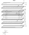
- FIG. 2 is an exploded perspective view of the multilayer board 10.
- FIG. 3 is a cross-sectional view of the multilayer board 10 in AA of FIG.
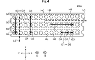
- FIG. 4 is a top view of the spacer 20a.
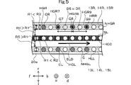
- FIG. 5 is a top view of the spacer 20a, the signal conductor layer SL, the ground conductor layers 13R, 14R, 15R, the ground conductor layers 13L, 14L, 15L, and the conductive material C.
- FIG. 6 is a diagram showing an inclusion relationship between the conductive material C and the through hole H1.
- FIG. 7 is a side view of the electronic device 1 including the multilayer board 10.
- FIG. 1 is a perspective view of the multilayer board 10 according to the embodiment of the first embodiment.
- FIG. 2 is an exploded perspective view of the multilayer board 10.
- FIG. 3 is a cross-sectional view of the multilayer board 10 in AA of FIG
- FIG. 8 is a top view of the electronic device 1 provided with the multilayer board 10.
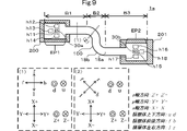
- FIG. 9 is a top view of the electronic device 1a including the multilayer board 100.
- FIG. 10 is a diagram showing a spacer 20a1 included in the multilayer substrate 10 according to the first modification of the first embodiment.
- FIG. 11 is a cross-sectional view taken along the line AA of the multilayer board 10a according to the second embodiment.
- FIG. 12 is a cross-sectional view taken along the line AA of the multilayer board 10a2 according to the embodiment of the second embodiment.
- FIG. 13 is a cross-sectional view taken along the line AA of the multilayer board 10b according to the embodiment of the third embodiment.
- FIG. 14 is a cross-sectional view taken along the line AA of the multilayer board 10c according to the embodiment of the fourth embodiment.
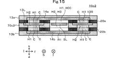
- FIG. 15 is a cross-sectional view taken along the line AA of the multilayer board 10c2 according to the first modification of the fourth embodiment.
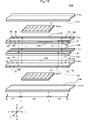
- FIG. 16 is an exploded perspective view of the multilayer board 10d according to the embodiment of the fifth embodiment.
- FIG. 17 is a side view of the multilayer board 10d according to the embodiment of the fifth embodiment.
- FIG. 18 is a side view of the multilayer board 10d2 according to the first modification of the fifth embodiment.
- FIG. 19 is a side view of the electronic device 2 provided with the multilayer board 10e according to the embodiment of the sixth embodiment.
- FIG. 20 is a top view of the electronic device 2 provided with the multilayer board 10e according to the embodiment of the sixth embodiment.
- FIG. 21 is a diagram of an electronic device 2a including the multilayer board 100e according to the embodiment of the sixth embodiment.
- FIG. 22 is a cross-sectional view taken along the line AA of the multilayer board 10f according to the embodiment of the seventh embodiment.
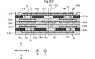
- FIG. 23 is a cross-sectional view taken along the line AA of the multilayer board 10 g according to the embodiment of the eighth embodiment.
- FIG. 24 is a top view of the spacer 21a according to the first modification of the spacer 20a.
- FIG. 25 is a top view of the spacer 22a according to a modified example of the spacer 21a.
- FIG. 26 is a top view of the spacer 22a, the signal conductor layer SL, the ground conductor layers 13R, 14R, 15R, and the ground conductor layers 13L, 14L, 15L.
- FIG. 27 is a top view of the spacer 23a according to the second modification of the spacer 20a.
- FIG. 28 is a top view of the spacer 24a according to the second modification of the spacer 20a.
- FIG. 29 is a top view of the spacer 25a according to the second modification of the spacer 20a.
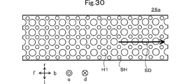
- FIG. 30 is a top view of the spacer 26a according to the third modification of the spacer 20a.
- FIG. 31 is a cross-sectional view taken along the line AA of the multilayer board 10h according to another embodiment.
- FIG. 32 is a cross-sectional view taken along the line AA of the multilayer board 10i according to another embodiment.
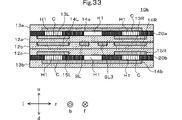
- FIG. 33 is a cross-sectional view taken along the line AA of the multilayer board 10k according to another embodiment.
- FIG. 34 is a cross-sectional view taken along the line AA of the multilayer board 10 m according to another embodiment.
- FIG. 35 is a cross-sectional view taken along the line AA of the multilayer board 10n according to another embodiment.
- FIG. 36 is a cross-sectional view taken along the line AA of the multilayer board 10p according to another embodiment.
- FIG. 37 is a cross-sectional view taken along the line AA of the multilayer board 10q according to another embodiment.
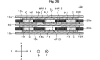
- FIG. 38 is a cross-sectional view taken along the line AA of the multilayer board 10r according to another embodiment.
- the direction is defined as follows.
- the stacking direction of the multilayer board 10 is defined as the vertical direction of the laminated body.
- the direction in which the signal conductor layer SL extends is defined as the left-right direction of the laminated body.
- the vertical direction of the laminated body and the horizontal direction of the laminated body are orthogonal to each other.
- the direction orthogonal to the vertical direction of the laminated body and the horizontal direction of the laminated body is defined as the front-rear direction of the laminated body.
- the definitions of the direction and the stacking direction in this specification are examples. Therefore, it is not necessary that the direction of the multilayer board 10 in actual use and the direction in the present specification match.
- X is a component or member of the multilayer board 10. Unless otherwise specified, each part of X is defined as follows in the present specification.
- the front part of X means the front half of X.
- the rear part of X means the rear half of X.
- the left part of X means the left half of X.
- the right part of X means the right half of X.
- the upper part of X means the upper half of X.
- the lower part of X means the lower half of X.
- the front end of X means the front end of X.
- the rear end of X means the rear end of X.
- the left end of X means the left end of X.
- the right end of X means the right end of X.
- the upper end of X means the upper end of X.
- the lower end of X means the lower end of X.
- the front end portion of X means the front end portion of X and its vicinity.
- the rear end portion of X means the rear end portion of X and its vicinity.
- the left end portion of X means the left end portion of X and its vicinity.
- the right end portion of X means the right end portion of X and its vicinity.
- the upper end portion of X means the upper end portion of X and its vicinity.
- FIG. 1 is a perspective view of the multilayer board 10 according to the embodiment of the first embodiment.
- FIG. 2 is an exploded perspective view of the multilayer board 10.
- FIG. 3 is a cross-sectional view of the multilayer board 10 in AA of FIG.
- FIG. 4 is a top view of the spacer 20a.
- the multilayer board 10 has a plate shape. Specifically, as shown in FIG. 1, the multilayer substrate 10 has a rectangular shape having long sides extending in the front-rear direction of the laminate when viewed in the vertical direction of the laminate. Therefore, the length of the multilayer board 10 in the front-rear direction of the laminate is longer than the length of the multilayer board 10 in the left-right direction of the laminate.
- the multilayer board 10 has mounting electrode portions EP1 and EP2 and an intermediate section CP.
- the intermediate section CP is a section other than the mounting electrode portions EP1 and EP2.
- the mounting electrode portion EP1 is located before the intermediate section CP. Therefore, the mounting electrode portion EP1 is located at the front end portion of the multilayer board 10.
- the mounting electrode portion EP2 is located after the intermediate section CP. Therefore, the mounting electrode portion EP2 is located at the rear end portion of the multilayer board 10.
- the width of the mounting electrode portions EP1 and EP2 in the left-right direction of the laminate is longer than the length of the width of the intermediate section CP in the left-right direction of the laminate.
- the shape of the multilayer board 10 is not limited to the shape shown in FIG.
- the multilayer substrate 10 is made by laminating a plurality of layers. Therefore, the multilayer substrate 10 includes a plurality of layers laminated in the vertical direction of the laminated body. Specifically, as shown in FIGS. 2 and 3, the multilayer substrate 10 includes the insulator layers 12a, 12b, 12c, 13a, 13b and the ground conductor layers 14a, 14b, 13R, 13L, 14R, 14L, 15R, It includes 15L, a signal conductor layer SL, spacers 20a and 20b, and interlayer connection conductors v1, v2, v3 and v4.
- the plurality of layers include, for example, the insulator layers 12a, 12b, 12c, 13a, 13b, the ground conductor layers 14a, 14b, 13R, 13L, 14R, 14L, 15R, 15L, and the signal conductor layer SL.
- the spacers 20a and 20b are included. Therefore, in the present embodiment, the multilayer substrate 10 includes the interlayer connecting conductors v1, v2, v3, v4 in addition to the plurality of layers. Further, in the present embodiment, the multilayer board 10 includes one or more insulator layers. One or more insulator layers include insulator layers 12a, 12b, 12c, 13a, 13b. In FIG. 2, the description of the front end portion and the rear end portion of the multilayer board 10 is omitted.
- the insulator layer 13b, the ground conductor layer 14b, the spacer 20b, the ground conductor layers 15R and 15L, the insulator layer 12c, the insulator layer 12b, and the signal conductor layer SL are laminated in this order toward the top of the laminate. Will be done. In other words, the ground conductor layer 14a is located above the spacer 20a in the vertical direction of the laminate. Further, the signal conductor layer SL is located below the spacer 20a in the vertical direction of the laminated body.
- the insulator layers 12a, 12b, 12c, 13a, 13b have a shape having long sides extending in the front-rear direction of the laminated body. As shown in FIG. 2, the insulator layers 12a, 12b, 12c, 13a, and 13b have a shape extending in the front-rear direction of the laminate when viewed in the vertical direction of the laminate. Therefore, the length of the insulator layers 12a, 12b, 12c, 13a, 13b in the left-right direction of the laminate is shorter than the length of the insulator layers 12a, 12b, 12c, 13a, 13b in the front-rear direction of the laminate.
- the insulator layers 12a, 12b, 12c, 13a, 13b are flexible dielectric sheets.
- the material of the insulator layers 12a, 12b, 12c, 13a, 13b is a thermoplastic resin, a fluororesin, or the like.
- the thermoplastic resin used as the material of the insulator layers 12a, 12b, 12c, 13a, 13b is a polyimide, a liquid crystal polymer, or the like.
- the fluororesin used as the material of the insulator layers 12a, 12b, 12c, 13a, 13b is specifically PTFE or the like.
- the ground conductor layer 14a has a shape having long sides extending in the front-rear direction when viewed in the vertical direction of the laminated body.
- the ground conductor layer 14a is arranged at the center of the lower main surface of the insulator layer 13a in the left-right direction of the laminated body.
- the width of the ground conductor layer 14a in the left-right direction of the laminate is substantially the same as that of the insulator layer 13a when viewed in the vertical direction of the laminate. However, the width of the ground conductor layer 14a in the left-right direction of the laminate is smaller than that of the insulator layer 13a when viewed in the vertical direction of the laminate.
- a ground is connected to the ground conductor layer 14a.
- the ground conductor layer 14b has a shape having a long side extending in the front-rear direction when viewed in the vertical direction of the laminated body.
- the ground conductor layer 14b is arranged at the center of the upper main surface of the insulator layer 13b in the left-right direction of the laminated body.
- the width of the ground conductor layer 14b in the left-right direction of the laminate is substantially the same as that of the insulator layer 13b when viewed in the vertical direction of the laminate. However, the width of the ground conductor layer 14b in the left-right direction of the laminate is smaller than that of the insulator layer 13b when viewed in the vertical direction of the laminate.
- a ground is connected to the ground conductor layer 14b.
- the signal conductor layer SL has a linear shape extending in the front-rear direction of the laminated body.
- the signal conductor layer SL is located below the spacer 20a.
- the signal conductor layer SL is arranged at the center of the upper main surface of the insulator layer 12b in the left-right direction of the laminated body.
- the width of the signal conductor layer SL in the left-right direction of the laminate is shorter than the width of the insulator layer 12b in the left-right direction of the laminate when viewed in the vertical direction of the laminate. ..
- the length of the width of the signal conductor layer SL in the left-right direction of the laminated body is, for example, about 170 ⁇ m.
- the signal conductor layer SL is located at a position overlapping with the ground conductor layer 14a in the vertical direction of the laminated body. Further, the signal conductor layer SL is located at a position overlapping with the ground conductor layer 14b in the vertical direction of the laminated body. As a result, the signal conductor layer SL and the ground conductor layers 14a and 14b have a microstrip line structure.
- the signal conductor layer SL is a kind of circuit pattern.
- the signal conductor layer SL is located at a position that does not overlap with the ground conductor layers 14R and 14L in the left-right direction of the laminated body.
- the ground conductor layer 13R has a linear shape extending in the front-rear direction of the laminated body.
- the ground conductor layer 13R is arranged on the right side of the upper main surface of the insulator layer 12a in the left-right direction of the laminated body.
- the width of the ground conductor layer 13R in the left-right direction of the laminate is shorter than the width of the insulator layer 12a in the left-right direction of the laminate when viewed in the vertical direction of the laminate.
- ground conductor layer 13L has the same configuration as the ground conductor layer 13R except that it is arranged on the left side of the laminated body in the left-right direction of the upper main surface of the insulator layer 12a, the description thereof will be omitted.
- the ground conductor layer 14R has a linear shape extending in the front-rear direction of the laminated body.
- the ground conductor layer 14R is arranged on the right side of the upper main surface of the insulator layer 12b in the left-right direction of the laminated body. Therefore, the ground conductor layer 14R is arranged to the right of the signal conductor layer SL in the left-right direction of the laminated body.
- the width of the ground conductor layer 14R in the left-right direction of the laminate is shorter than the width of the insulator layer 12b in the left-right direction of the laminate when viewed in the vertical direction of the laminate. ..
- the ground conductor layer 14R is located at a position that does not overlap the signal conductor layer SL and the ground conductor layer 14L in the left-right direction of the laminated body.
- the ground conductor layer 14L has a linear shape extending in the front-rear direction of the laminated body.
- the ground conductor layer 14L is arranged on the left portion of the upper main surface of the insulator layer 12b in the left-right direction of the laminated body. Therefore, the ground conductor layer 14L is arranged to the left of the signal conductor layer SL in the left-right direction of the laminated body.
- the width of the ground conductor layer 14L in the left-right direction of the laminate is shorter than the width of the insulator layer 12b in the left-right direction of the laminate when viewed in the vertical direction of the laminate. ..
- the ground conductor layer 14L is located at a position not overlapping the signal conductor layer SL and the ground conductor layer 14R in the left-right direction of the laminated body.
- the ground conductor layer 15R has a linear shape extending in the front-rear direction of the laminated body.
- the ground conductor layer 15R is arranged on the right side of the lower main surface of the insulator layer 12c in the left-right direction of the laminated body.
- the width of the ground conductor layer 13R in the left-right direction of the laminate is shorter than the width of the insulator layer 12a in the left-right direction of the laminate when viewed in the vertical direction of the laminate. ..
- ground conductor layer 15L has the same configuration as the ground conductor layer 15R except that it is arranged on the left side of the laminated body in the left-right direction on the lower main surface of the insulator layer 12c, the description thereof will be omitted.
- the width of the ground conductor layers 13R, 13L, 14R, 14L, 15R, 15L in the left-right direction of the laminated body is, for example, about 300 ⁇ m.
- the interlayer connection conductors v1 and v4 are located to the right of the signal conductor layer SL as shown in FIG.
- the interlayer connecting conductor v1 is located before the interlayer connecting conductor v4.
- the upper ends of the interlayer conductors v1 and v4 are connected to the ground conductor layer 13R.
- the lower ends of the interlayer conductors v1 and v4 are connected to the ground conductor layer 15R.
- the interlayer connecting conductors v1 and v4 electrically connect the ground conductor layer 13R, the ground conductor layer 14R, and the ground conductor layer 15R.
- the interlayer connection conductors v2 and v3 are located to the left of the signal conductor layer SL as shown in FIG.
- the interlayer connecting conductor v2 is located before the interlayer connecting conductor v3.
- the upper ends of the interlayer conductors v2 and v3 are connected to the ground conductor layer 13L.
- the lower ends of the interlayer conductors v2 and v3 are connected to the ground conductor layer 15L.
- the interlayer connecting conductors v2 and v3 electrically connect the ground conductor layer 13L, the ground conductor layer 14L, and the ground conductor layer 15L.
- the interlayer connection conductors v1 to v4 are through-hole conductors.
- the through-hole conductor is formed by plating the through holes formed in the insulator layers 12a, 12b, and 12c.
- the interlayer connection conductors v1 to v4 may be via hole conductors.
- the via hole conductor is formed by filling the through holes H1 formed in the insulator layers 12a, 12b, and 12c with the conductive paste and sintering the conductive paste.
- each of the interlayer connecting conductors v1 formed between the layers does not necessarily have to overlap when viewed from the vertical direction of the laminated body.
- the position of the interlayer connecting conductor v1 formed between the insulator layer 12a and the insulator layer 12b is such that the position of the interlayer connecting conductor v1 is the insulator layer 12a when viewed from the vertical direction of the laminate. It may be different from the position of the interlayer connection conductor v1 formed between the insulator layer 12b and the insulator layer 12b.
- interlayer connecting conductors v2 to v4 are via hole conductors
- the interlayer connecting conductor v1 is a via hole conductor. Therefore, the description when the interlayer connection conductors v2 to v4 are via hole conductors will be omitted.
- the spacers 20a and 20b have a plate shape having long sides extending in the front-rear direction. As shown in FIG. 2, the spacers 20a and 20b have a shape extending in the front-rear direction of the laminated body when viewed in the vertical direction of the laminated body. Therefore, the length of the spacers 20a and 20b in the left-right direction of the laminated body is shorter than the length of the spacers 20a and 20b in the front-rear direction of the laminated body.
- the spacer 20a is located below the ground conductor layer 14a. Further, the spacer 20a is located above the signal conductor layer SL.
- the spacers 20a and 20b are made of a material having a low dielectric constant and a low dielectric loss tangent (for example, LCP, PTFE, etc.). As a result, the transmission loss of the high frequency signal flowing through the multilayer board 10 can be reduced.
- the materials of the spacers 20a and 20b are the same as those of the insulator layers 12a, 12b, 12c, 13a and 13b (thermoplastic resin such as polyimide or liquid crystal polymer). In other words, the materials of the spacers 20a and 20b and the materials of the insulator layers 12b, 12c and 13b located below the signal conductor layer SL are the same, and the materials of the spacers 20a and 20b and the signal conductor layer are the same.
- the materials of the insulator layers 12a and 13b located above the SL are the same.
- the coefficient of thermal expansion of the spacers 20a and 20b is the same as the coefficient of thermal expansion of the insulator layers 12a, 12b, 12c, 13a and 13b.
- a phenomenon that only the spacers 20a and 20b are deformed by heat is unlikely to occur. Therefore, by using the same material for the spacers 20a and 20b and the materials for the insulator layers 12a, 12b, 12c, 13a and 13b, it is possible to prevent the spacers 20a and 20b from being warped and the like. be.
- the spacer 20a has a plurality of through holes H1 that penetrate the spacer 20a in the vertical direction of the laminated body.
- the diameter of the through hole H1 is longer than the thickness of the spacers 20a and 20b in the vertical direction of the laminate.
- the length of the maximum diameter of the through hole H1 when viewed in the vertical direction of the laminated body is longer than the length of the thickness of the spacers 20a and 20b in the vertical direction of the laminated body.
- the diameter of the through hole H1 is longer than the thickness of the spacers 20a and 20b in the vertical direction of the laminated body.
- the maximum diameter of the elliptical through hole H1 is longer than the thickness of the spacers 20a and 20b in the vertical direction of the laminate.
- only one through hole is designated by a reference numeral. Therefore, in FIG. 4, all the through holes are not designated as H1.
- the spacer 20b has the same configuration as the spacer 20a except that it is located above the ground conductor layer 14b and below the signal conductor layer SL. Therefore, the description of the spacer 20b will be omitted.
- each through hole H1 is the same.
- the shape of the through hole H1 has a circular shape when viewed in the vertical direction of the laminated body.
- a plurality of through holes H1 are formed over the entire spacer 20a. Specifically, first, as shown in FIG. 4, a direction FD parallel to the first straight line L1 is defined on the spacer 20a. The plurality of through holes H1 are arranged along the direction FD. For example, as shown in FIG. 4, 13 through holes H1 are arranged along the direction FD.
- the direction FD coincides with, for example, the extending direction of the signal conductor layer SL. However, the extending direction of the signal conductor layer SL and the direction FD do not necessarily have to match.
- the multilayer board 10 has a plurality of sets of through holes H1.
- the three sets include the sets GL, GC, and GR (see FIG. 4).
- a plurality of through holes H1 belonging to the set GL are referred to as a plurality of through holes HL.
- a plurality of through holes H1 belonging to the set GC are referred to as a plurality of through holes HC.
- a plurality of through holes H1 belonging to the set GR are referred to as a plurality of through holes HR.
- a direction SD parallel to the second straight line L2, which is not parallel to the first straight line L1 is defined on the spacer 20a.
- the set GR, GC, GL of the plurality of through holes H1 are arranged along the direction SD different from the direction FD.
- the direction SD coincides with, for example, the width direction of the signal conductor layer SL.
- the width direction and the direction SD of the signal conductor layer SL do not necessarily have to match.
- the plurality of through holes H1 are provided in the spacer 20a in a matrix.
- the direction FD and the direction SD are orthogonal to each other.
- the direction FD and the direction SD do not have to be orthogonal to each other.
- the arrangement of the plurality of through holes H1 will be described in more detail.
- the intervals between the plurality of adjacent through holes H1 in the direction FD are uniform.
- the distance between the centers of gravity of the adjacent through holes H1 in the plurality of through holes H1 arranged along the direction FD is uniform.
- the distance between the centers of gravity of the adjacent through holes H1 in the plurality of through holes H1 arranged along the direction FD is about 250 ⁇ m.
- the center of gravity of each of the three through holes H1 arranged along the direction FD is defined as the center of gravity G1, G2, G3.
- the through hole H1 that defines the center of gravity G1 and the through hole H1 that defines the center of gravity G2 are adjacent to each other.
- the through hole H1 that defines the center of gravity G2 and the through hole H1 that defines the center of gravity G3 are adjacent to each other.
- the length of the distance D1 between the center of gravity G1 and the center of gravity G2 and the length of the distance D2 between the center of gravity G2 and the center of gravity G3 are equal.
- the spacing between the plurality of adjacent through holes H1 in the direction SD is uniform.
- the distance between the centers of gravity of the adjacent through holes H1 in the plurality of through holes H1 arranged along the direction SD is uniform.
- the distance between the centers of gravity of the adjacent through holes H1 in the plurality of through holes H1 arranged along the direction SD is about 405 ⁇ m.
- the center of gravity of each of the three through holes H1 arranged along the direction SD is defined as the center of gravity G4, G5, G6.
- the through hole H1 that defines the center of gravity G4 and the through hole H1 that defines the center of gravity G5 are adjacent to each other.
- the through hole H1 that defines the center of gravity G5 and the through hole H1 that defines the center of gravity G6 are adjacent to each other.
- the length of the distance D3 between the center of gravity G4 and the center of gravity G5 and the length of the distance D4 between the center of gravity G5 and the center of gravity G6 are equal.
- FIG. 5 is a top view of the spacer 20a, the signal conductor layer SL, the ground conductor layers 13R, 14R, 15R, the ground conductor layers 13L, 14L, 15L, and the conductive material C.
- FIG. 5 is a perspective view of the signal conductor layer SL, the ground conductor layers 13R, 14R, 15R and the ground conductor layers 13L, 14L, 15L.
- FIG. 6 is a diagram showing an inclusion relationship between the conductive material C and the through hole H1.
- the length of the diameter of the plurality of through holes H1 is shorter than the length of the width between the signal conductor layer SL and the ground conductor layers 13R, 14R, 15R.
- the length R1 of the diameters of the plurality of through holes H1 is the distance between the right end of the signal conductor layer SL and the left end of the ground conductor layers 13R, 14R, 15R in the left-right direction of the laminate. Is shorter than R4.
- the length R4 is, for example, about 170 ⁇ m.
- the length R1 of the diameters of the plurality of through holes H1 is the distance between the left end of the signal conductor layer SL and the right end of the ground conductor layers 13R, 14R, 15R in the left-right direction of the laminate. It is shorter than the length R5.
- the length R5 is, for example, about 170 ⁇ m.
- the plurality of through holes H1 include a plurality of through holes HCC (first hollow through holes) that overlap with the signal conductor layer SL when viewed from the vertical direction of the laminated body.
- the plurality of through holes HCC are arranged along the direction FD. At least one of the plurality of through holes HCC is hollow. However, in the example shown in FIG. 5, all the through holes HCC are hollow.
- the diameter length R1 of the plurality of through holes HCC is larger than the width length R2 of the signal conductor layer SL in the left-right direction of the laminate when viewed in the vertical direction of the laminate. short.
- the through hole H1 when the shape of the through hole H1 is circular when viewed in the vertical direction of the laminated body, the diameter of the through hole H1 is shorter than the length R2. Further, for example, when the shape of the through hole H1 is elliptical when viewed in the vertical direction of the laminated body, the maximum diameter of the elliptical through hole H1 is shorter than the length R2. As a result, the through hole HCC is included in the signal conductor layer SL when viewed from the vertical direction of the laminated body.
- the plurality of through holes H1 include a plurality of through holes HRR that overlap with the ground conductor layers 13R, 14R, and 15R when viewed from the vertical direction of the laminated body.
- the diameter length R1 of the plurality of through holes HRR is shorter than the width length R3 of the ground conductor layers 13R, 14R, and 15R in the left-right direction of the laminated body.
- the through hole HRR is included in the ground conductor layers 13R, 14R, 15R when viewed from the vertical direction of the laminated body.
- the plurality of through holes H1 include a plurality of through holes HLL that overlap with the ground conductor layers 13L, 14L, and 15L when viewed from the vertical direction of the laminated body.
- the diameter length R1 of the plurality of through holes HLL is shorter than the width length R3 of the ground conductor layers 13L, 14L, and 15L in the left-right direction of the laminated body.
- the through hole HLL is included in the ground conductor layers 13L, 14L, and 15L when viewed from the vertical direction of the laminated body.
- the through hole H1 does not necessarily have to be included in the signal conductor layer SL, the ground conductor layers 13R, 14R, 15R and the ground conductor layers 13L, 14L, 15L when viewed from the vertical direction of the laminated body.
- a part of the through hole H1 when viewed from the vertical direction of the laminated body overlaps the signal conductor layer SL, the ground conductor layers 13R, 14R, 15R and the ground conductor layers 13L, 14L, 15L when viewed from the vertical direction of the laminated body. Just do it.
- a plurality of conductive materials C are provided in a part of the plurality of through holes H1.
- the conductive material C is, for example, solder or a conductive adhesive.
- solder is used as the conductive material C, moisture absorption or the like is unlikely to occur in the solder. Therefore. It is possible to increase the reliability of the connection.
- a conductive adhesive is used as the conductive material C, reflow is not required. Therefore, it is possible to use a material having low heat resistance for the multilayer board 10.
- the plurality of conductive materials C include a plurality of conductive materials CL and a plurality of conductive materials CR.
- the conductive materials CL and CR will be described.
- the signal conductor layer SL, the ground conductor layers 13R, 14R, 15R, the ground conductor layers 13L, 14L, 15L, and the conductive material C are shown in a dot pattern.
- the plurality of conductive material CRs are provided in a part of the plurality of through holes HRR.
- the ground conductor layer 13R and the ground conductor layer 14a are electrically connected by the conductive material CR.
- the through hole provided with the conductive material CR in the through hole HRR is referred to as a through hole HGR (see FIG. 6).
- the through hole in which the conductive material CR is not provided in the through hole HRR is referred to as a through hole NHGR (see FIG. 6).
- the plurality of through holes HGR are arranged along the extending direction SLD of the signal conductor layer SL (see FIG. 5). Similarly, the plurality of through holes NHGR are aligned along the directional SLD. In the example shown in FIG. 5, the direction SLD and the direction FD coincide with each other. However, the direction SLD and the direction FD do not necessarily have to match.
- the through holes HGR and the through holes NHGR are alternately arranged along the direction SLD.
- the through holes HGR and the through holes NHGR do not necessarily have to be arranged alternately.
- the plurality of conductive material CRs may be continuously provided in the through holes HRR in the front-rear direction of the laminated body (the through holes HGR may be continuously arranged).
- the conductive material CR may be provided in each of the three through holes HRR that are continuously arranged in the direction SLD.
- the conductive material CR can be provided so as to be dense. Therefore, the strength of the multilayer board 10 can be increased, and the shielding property against the signal conductor layer SL can be enhanced.
- the plurality of conductive material CLs are provided in a part of the plurality of through holes HLL as shown in FIG.
- the ground conductor layer 13L and the ground conductor layer 14a are electrically connected by the conductive material CL.
- the through hole provided with the conductive material Cl in the through hole HLL is referred to as a through hole HGL.
- the through hole in which the conductive material CL is not provided in the through hole HLL is referred to as a through hole NHGL.
- a plurality of through hole HGLs are arranged along the direction SLD in the same manner as the through hole HGR. Further, the plurality of through holes NHGR are arranged along the direction SLD.
- the through holes HGL and the through holes NHGL are alternately arranged along the direction SLD.
- the through hole HGL may be continuously arranged.
- the conductive material CR can be densely provided. Therefore, the strength of the multilayer board 10 can be increased, and the shielding property against the signal conductor layer SL can be enhanced.
- the spacer 20a is provided with at least one set of through holes H1 provided with adjacent conductive materials C when viewed from the vertical direction of the laminated body. Then, in the set of through holes H1 provided with at least one set of adjacent conductive materials C, the spacing between the through holes H1 provided with the conductive material C becomes uniform. In other words, in a set of through holes H1 provided with at least one set of adjacent conductive materials C, the distance between the centers of gravity of the through holes H1 provided with the conductive material C becomes uniform.
- a set of three adjacent through holes HGR7, HGR8, and HGR9 is defined.
- the through holes HGR7, HGR8, and HGR9 form a set of through holes HGR.
- the centers of gravity G7, G8, and G9 are defined for each of the sets of the adjacent through holes HGR7, HGR8, and HGR9.
- the length of the distance D5 between the center of gravity G7 and the center of gravity G8 and the length of the distance D6 between the center of gravity G8 and the center of gravity G9 are equal.
- the spacer 20a may be provided with a set of through holes HGL having uniform intervals.
- the spacer 20a may be provided with a set of through holes HGL having a uniform distance between the centers of gravity in the same manner as the set of through holes HGR.
- the spacer 20a may be provided with at least one set of through hole HGR having a uniform spacing of at least one set or a set of through holes HGL having a uniform spacing of at least one set.
- the spacer 20a has at least one set of through holes HGR having a uniform distance between at least one set of centers of gravity, or at least one set of through holes HGL having a uniform distance between at least one set of centers of gravity. It suffices if it is provided.
- FIG. 7 is a side view of the electronic device 1 including the multilayer board 10.
- FIG. 8 is a top view of the electronic device 1 provided with the multilayer board 10.
- the multilayer board 10 transmits a high frequency signal. Therefore, as shown in FIGS. 7 and 8, the multilayer board 10 is used in the electronic device 1 to connect the circuit board 200 and the circuit board 201.
- the multilayer board 10 is used for connecting two circuit boards in an electronic device such as a mobile phone.
- the connector 301 is mounted on the circuit board 200. Further, as shown in FIG. 7, a connector 303 is mounted on the circuit board 201.
- the upper resist layer 18a exists above the multilayer substrate 10.
- the upper resist layer 18a covers substantially the entire surface of the upper main surface of the insulator layer 13a.
- the lower resist layer 18b exists below the multilayer substrate 10.
- the lower resist layer 18b covers substantially the entire lower main surface of the insulator layer 13b.
- the lower resist layer 18b is provided with openings h11 to h18.
- the openings h11 to h14 overlap with the mounting electrode portion EP1 when viewed in the vertical direction of the laminated body.
- the openings h15 to h18 overlap with the mounting electrode portion EP2 when viewed in the vertical direction of the laminated body.
- the multilayer substrate 10 includes external electrodes 30a and 30b.
- the external electrodes 30a and 30b are electrically connected to the signal conductor layer SL.
- the description of the external electrodes 30a and 30b is omitted.
- the external electrode 30a overlaps with the opening h11 in the vertical direction of the laminate.
- the external electrode 30b is exposed from the opening h11. Further, the external electrode 30b overlaps with the opening h15 in the vertical direction of the laminated body. The external electrode 30b is exposed from the opening h15.
- the ground conductor layer 14b overlaps the openings h11 to h13 and the openings h16 to h18.
- the ground conductor layer 14b is exposed from the openings h11 to h13 and the openings h16 to h18.
- the connector 300 is mounted on the lower main surface of the multilayer board 10 in the mounting electrode portion EP1. More specifically, the connector 300 is mounted on the external electrode 30a and the ground conductor layer 14b exposed from the opening h11. Further, as shown in FIG. 7, the connector 302 is mounted on the lower main surface of the multilayer board 10 in the mounting electrode portion EP2. More specifically, the connector 302 is mounted on the external electrode 30b and the ground conductor layer 14b exposed from the opening h15.
- Each of the connectors 300 and 302 is connected to the connectors 301 and 303.
- the signal conductor layer SL of the multilayer board 10 is electrically connected to the circuit board 200 via the external electrode 30a. Further, the signal conductor layer SL of the multilayer board 10 is electrically connected to the circuit board 201 via the external electrode 30b.
- the multilayer board 10 has flexibility. Therefore, it is possible to bend the multilayer board 10. Therefore, the multilayer board 10 can be used in a bent state in an electronic device. Hereinafter, the bent multilayer board 10 will be described in more detail.
- the multilayer board 10 When the multilayer board 10 is bent, as shown in FIGS. 7 and 8, the multilayer board 10 has non-curved sections A1 and A3 and curved sections A2.
- the x-axis direction, the y-axis direction, and the z-axis direction in the multilayer board 10 are defined as follows.
- the x-axis direction is the left-right direction of the laminated body in the non-curved section A1.
- the y-axis direction is the anteroposterior direction of the laminated body in the non-curved section A1.
- the z-axis direction is the vertical direction of the laminated body in the non-curved section A1.
- the non-curved sections A1 and A3 are sections in which the multilayer board 10 is not bent.
- the curved section A2 is a section in which the multilayer board 10 is bent.
- the multilayer board 10 is bent in the z-axis direction in the curved section A2.
- the non-curved sections A1 and A3 are adjacent to the curved section A2.
- the non-curved section A1 is located in front of the curved section A2.
- the non-curved section A3 is located after the curved section A2.
- bending means bending by receiving an external force.
- the vertical direction of the laminated body and the front-back direction of the laminated body differ depending on the position of the multilayer board 10.
- the non-curved section A1 that is not bent in the z-axis direction for example, the position of (1) in FIG. 7
- the vertical direction of the laminated body and the front-rear direction of the laminated body coincide with each of the z-axis direction and the y-axis direction. do.
- the curved section A2 for example, the position of (2) in FIG.
- the bent multilayer board 10 also has flexibility. Therefore, the multilayer board 10 bent in the z-axis direction can be further bent in the z-axis direction.
- the multilayer board according to the present invention may be a multilayer board 100 that is bent in an arc shape in the x-axis direction.
- the multilayer board 100 will be described in detail with reference to the drawings.
- FIG. 9 is a top view of the electronic device 1a including the multilayer board 100.
- bending in an arc means having a bent shape without receiving an external force.
- the multilayer board 100 can connect the circuit board 200 and the circuit board 201 in a state of being bent in an arc shape in the x-axis direction in an electronic device. As shown in FIG. 9, the multilayer board 100 is used for connecting the circuit board 200 and the circuit board 201 in the electronic device 1a.
- the multilayer board 100 has non-curved sections B1 and B3 and curved sections B2.
- the non-curved sections B1 and B3 are sections in which the multilayer board 100 is not bent in an arc shape in the x-axis direction.
- the curved section B2 is a section including a portion where the multilayer board 100 bends in an arc shape in the x-axis direction.
- the non-curved sections B1 and B3 are adjacent to the curved section B2.
- the non-curved section B1 is located before the curved section B2.
- the non-curved section B3 is located after the curved section B2.
- the vertical direction of the laminated body and the front-back direction of the laminated body differ depending on the position of the multilayer board 100 as shown in FIG.
- the non-curved section B1 for example, the position (1) in FIG. 9 that bends in an arc shape in the x-axis direction
- the vertical direction of the laminated body and the front-rear direction of the laminated body coincide with each of the z-axis direction and the y-axis direction. .
- the curved section B2 for example, the position of (2) in FIG.
- the multilayer substrate 100 bends in an arc shape in the x-axis direction, the z-axis direction and the y-axis are respectively in the vertical direction of the laminated body and the front-rear direction of the laminated body. Does not match each of the directions.
- the multilayer board 100 can connect the circuit board 200 and the circuit board 201 in a state of being bent in an arc shape in the x-axis direction in the electronic device 1.
- the through holes H1 are uniformly provided in the curved section B2 of the multilayer board. Therefore, even in the multilayer board having the curved section B2, the possibility that the impedance of the signal conductor layer SL deviates from the predetermined impedance can be reduced.
- the multilayer board 100 is manufactured, for example, by cutting one board into a shape that bends in an arc shape on an x-axis.
- the multilayer board 100 bent in an arc shape in the x-axis direction also has flexibility. Therefore, it is possible to further bend the multilayer board 100 in a state of being bent in an arc shape in the x-axis direction in the z-axis direction.
- the configuration of the multilayer board 100 is the same as the configuration of the multilayer board 10 except that it is bent in an arc shape in the x-axis direction, the description thereof will be omitted.
- the multilayer board 10 includes spacers 20a and 20b provided with a plurality of through holes H1. As a result, a region having a low dielectric constant (through hole H1) is uniformly formed in the spacers 20a and 20b. As a result, in the region where the spacers 20a and 20b are provided in the multilayer board 10, the dielectric loss of the high frequency signal transmitted through the signal conductor layer SL is reduced. Therefore, the transmission loss of the high frequency signal is reduced. As a result, it is possible to increase the high frequency of the high frequency signal transmitted through the signal conductor layer SL.
- the multilayer board 10 it is possible to suppress the deviation of the characteristic impedance of the multilayer board 10. More specifically, when viewed in the vertical direction of the laminated body, the distance between the centers of gravity of the adjacent through holes H1 in the direction FD is uniform. Further, when viewed in the vertical direction of the laminated body, the distance between the centers of gravity of the adjacent through holes H1 in the direction SD is uniform. As a result, a region having a low dielectric constant is uniformly formed on the spacers 20a and 20b. As a result, the dielectric constant of the multilayer board 10 can be uniformly lowered in the region where the spacers 20a and 20b are provided in the multilayer board 10. Therefore, it is possible to suppress the deviation of the characteristic impedance of the multilayer board 10.
- At least one hollow through hole H1 overlaps with the signal conductor layer SL when viewed in the vertical direction of the laminate. Since air is present in the hollow through hole H1, the dielectric constant in the hollow through hole H1 is low. Therefore, according to the multilayer board 10, it is possible to reduce the dielectric constant around the signal conductor layer SL.
- the multilayer board 10 it is possible to suppress the deviation of the characteristic impedance of the multilayer board 10.
- the multilayer board 10 and the multilayer board without the spacers 20a and 20b (hereinafter referred to as Comparative Example 1) will be compared and described.
- a hollow portion formed by air is formed between the signal conductor layer and the ground conductor layer.
- the hollow portion is a region surrounded by a plurality of insulator layers, a signal conductor layer, and a ground conductor layer.
- a large region (hollow portion) formed by air is formed on the multilayer substrate.
- the multilayer board 10 includes spacers 20a and 20b provided with a plurality of through holes H1.
- the plurality of through holes H1 are regions formed by air.
- a small region (through hole H1) formed by air is formed in the multilayer substrate 10.
- a part of the spacers 20a and 20b is located around the through hole H1.
- a part of the spacer 20a supports the ground conductor layer 14a and the insulator layer 12a.
- the through hole H1 located between the ground conductor layer 14a and the insulator layer 12a is less likely to be crushed.
- the spacer 20b makes it difficult for the through hole H1 located between the ground conductor layer 14b and the insulator layer 12c to be crushed.
- the possibility that the through hole H1 is crushed is low. Therefore, it is unlikely that the positional relationship (distance, etc.) between the signal conductor layer SL and the ground conductor layer 14a will change when the through hole H1 is crushed when viewed in the vertical direction of the laminated body.
- the multilayer board 10 can suppress the deviation of the characteristic impedance of the multilayer board 10.
- the distance between the centers of gravity of the adjacent through holes H1 in the plurality of through holes H1 arranged along the direction FD is uniform. Therefore, when stress is applied to the spacers 20a and 20b, the stress applied to the spacers 20a and 20b tends to be uniform. Therefore, local deformation is unlikely to occur in the spacers 20a and 20b. Therefore, it is unlikely that the through hole H1 will be crushed due to local deformation of the spacers 20a and 20b. Therefore, it is unlikely that the positional relationship (distance, etc.) between the signal conductor layer SL and the ground conductor layer 14a will change when viewed in the vertical direction of the layer. As a result, the multilayer board 10 can suppress the deviation of the characteristic impedance of the multilayer board 10.
- the multilayer board 10 is easily bent. More specifically, in the multilayer board 10, the plurality of through holes H1 are arranged along the direction FD. Further, the multilayer board 10 has a plurality of sets of through holes H1. With the above configuration, the number of through holes H1 included in the multilayer board 10 increases. That is, the space (through hole H1) formed by air increases. Therefore, the spacer 20a is easily bent. As a result, the multilayer board 10 is easily bent.
- the multilayer board 10 is easily bent. More specifically, when viewed from the vertical direction of the laminated body, the distance between the centers of gravity of the adjacent through holes H1 in the plurality of through holes H1 arranged along the direction FD is uniform. Further, when viewed from the vertical direction of the laminated body, the distance between the centers of gravity of the adjacent through holes H1 in the plurality of through holes H1 arranged along the direction SD is uniform. As a result, when the spacer 20a is bent, the corner portion of the spacer 20a and the through hole H1 are likely to overlap each other when viewed from the vertical direction of the laminated body. Therefore, the spacer 20a is easily bent. As a result, the multilayer board 10 is easily bent.
- the electronic device 1 provided with the multilayer board 10 it is possible to increase the high frequency of the high frequency signal transmitted through the signal conductor layer SL, and it is possible to suppress the deviation of the characteristic impedance of the electronic device 1. ..
- the ground conductor layer 14a and the ground conductor layers 13R and 13L can be connected without using the interlayer connecting conductor.
- the multilayer substrate 10 includes a ground conductor layer 14a located above the spacer 20a in the vertical direction of the laminate. Further, the multilayer substrate 10 includes ground conductor layers 13R and 13L located below the spacer 20a in the vertical direction of the laminate.
- the multilayer substrate 10 includes a plurality of conductive materials C. The plurality of conductive materials C connect the ground conductor layer 14a and the ground conductor layers 13R and 13L via the spacer 20a. As described above, the plurality of conductive materials C of the spacer 20a can connect the ground conductor layer 14a and the ground conductor layers 13R and 13L without using an interlayer connecting conductor.
- the characteristic impedance of the signal conductor layer SL is unlikely to change.
- the plurality of through holes H1 provided with the conductive material C are arranged along the direction SLD.
- the spacers 20a and 20b are provided with at least one set of through holes H1 provided with adjacent conductive materials C when viewed from the vertical direction of the laminated body. Then, in the set of through holes H1 provided with at least one set of adjacent conductive materials C, the distance between the centers of gravity of the plurality of through holes H1 provided with the conductive materials C becomes uniform. In this case, the conductive materials C are lined up at equal intervals. Therefore, unevenness is unlikely to occur in the capacity of electricity generated between the signal conductor layer SL and the conductive material C. Therefore, the characteristic impedance of the signal conductor layer SL is unlikely to fluctuate.
- the spacer 20a can be easily manufactured. More specifically, the shapes of the plurality of through holes H1 are the same. This makes it possible to continuously form the plurality of through holes H1 by the same processing method. Therefore, the process of manufacturing the spacers 20a and 20b can be simplified. Therefore, the spacer 20a can be easily manufactured.
- the materials of the spacers 20a and 20b of the multilayer board 10 are the same as the materials of the insulator layers 12a, 12b and 12c.
- the coefficient of thermal expansion of the spacers 20a and 20b and the coefficient of thermal expansion of the insulator layers 12a, 12b and 12c are the same. Therefore, the multilayer board 10 is less likely to warp during heating (such as during a heating press when the multilayer boards 10 are laminated).
- the multilayer board 10 having the curved section A2 by providing the spacers 20a and 20b, it is possible to suppress the deviation of the characteristic impedance of the multilayer board 10.
- a multilayer board 10 having a curved section A2 and having spacers 20a and 20b, and a multilayer board having a curved section that bends in the z-axis direction and not having spacers 20a and 20b hereinafter, it will be referred to as Comparative Example 2 and will be described in comparison.
- a hollow portion formed by air is formed between the signal conductor layer and the ground conductor layer. Then, when the multilayer board is bent in the z-axis direction to form a curved section, pressure is applied to the hollow portion located in the curved section that bends in the z-axis direction. At this time, in the curved section that bends in the z-axis direction, the hollow forming a large air region is likely to collapse. When the hollow portion is crushed, the positional relationship (distance, etc.) between the signal conductor layer and the ground conductor layer may change when viewed from the vertical direction of the laminated body. As a result, the characteristic impedance of the multilayer board may shift.
- the spacers 20a and 20b having a plurality of through holes H1 are formed at the positions of the curved section A2. That is, a small region (through hole H1) formed by air is formed in the multilayer substrate 10 in the curved section A2.
- a small region (through hole H1) formed by air is formed in the multilayer substrate 10 in the curved section A2.
- the diameter length R1 of the through hole H1 is shorter than the width length R2 of the signal conductor layer SL in the left-right direction of the laminate.
- the distance between the through hole HCC that overlaps the signal conductor layer SL when viewed in the vertical direction of the laminated body and the through hole HGR that overlaps the ground conductor layer 13R when viewed in the vertical direction of the laminated body becomes long. Therefore, the distance between the through hole HCC and the conductive material CR provided in the through hole HGR becomes long when viewed in the vertical direction of the laminated body.
- the diameter length R1 of the through hole H1 is longer than the thickness length of the spacers 20a and 20b in the vertical direction of the laminated body. In this case, the size of the through hole H1 is large with respect to the thickness of the spacers 20a and 20b. Therefore, when the multilayer board 10 is bent or the like, the through hole H1 is less likely to be blocked.
- the diameter length R1 of the through hole H1 is shorter than the distance length R4 between the right end of the signal conductor layer SL and the left end of the ground conductor layers 13R, 14R, 15R in the left-right direction of the laminate. Further, the length R1 of the diameter of the through hole H1 is shorter than the length R5 of the distance between the left end of the signal conductor layer SL and the right end of the ground conductor layers 13L, 14L, 15L in the left-right direction of the laminate.
- the through hole H1 is not formed in the through hole H1 so as to overlap both the signal conductor layer SL and the ground conductor layers 13R and 13L when viewed from the vertical direction of the laminated body. Therefore, the conductive material C is formed so as not to overlap the signal conductor layer SL when viewed from the vertical direction of the laminated body. As a result, the multilayer board 10 makes it possible to suppress the deviation of the characteristic impedance of the signal conductor layer SL generated by the conductive material C.
- the insulator layer 13a to which the metal foil layer is attached to the lower main surface, the insulator layer 13b to which the metal foil layer is attached to the upper main surface, and the metal foil layer to the upper main surface are provided.
- the attached insulator layer 12a, the insulator layer 12b to which the metal foil layer is attached to the upper main surface, and the insulator layer 12c to which the metal foil layer is attached to the upper main surface are prepared.
- the ground conductor layer 14a is formed by etching the metal foil layer attached to the lower main surface of the insulator layer 13a.
- the ground conductor layer 14b is formed by etching the metal foil layer attached to the upper main surface of the insulator layer 13b.
- the ground conductor layers 13R and 13L are formed by etching the metal foil layer attached to the upper main surface of the insulator layer 12a.
- the signal conductor layer SL, the ground conductor layers 14R and 14L and the external electrodes 30a and 30b are formed by etching the metal foil layer attached to the upper main surface of the insulator layer 12b.
- the ground conductor layers 15R and 15L are formed by etching the metal foil layer attached to the upper main surface of the insulator layer 12c.
- the surface of the ground conductor layer 14a in contact with the insulator layer 13a is roughened. Therefore, the surface roughness of the surface of the ground conductor layer 14a that is in contact with the insulator layer 13a is coarser than the surface roughness of the surface of the ground conductor layer 14a that is not in contact with the insulator layer 13a. As a result, the ground conductor layer 14a and the insulator layer 13a are less likely to come off. Similarly, the ground conductor layer 14b and the insulator layer 13b are not easily peeled off.
- the third step through holes are formed in the insulator layers 12a, 12b, 12c. Then, by forming the conductor in the through hole by the plating treatment, the interlayer connection conductors v1 to v4 are formed.
- the process of forming the through hole is, for example, formation by irradiation with a laser beam, formation by a drill, or the like.
- a plate-shaped insulator made of a thermoplastic resin such as polyimide or a liquid crystal polymer is prepared. Then, a process is performed to form a through hole H1 in the plate-shaped insulator. As a result, spacers 20a and 20b provided with through holes H1 are created.
- the processing for forming the through hole H1 is, for example, processing with a drill or etching processing with a chemical agent.
- the shapes of the through holes H1 are all the same, and the distances between the adjacent through holes H1 are evenly spaced. Thereby, a plurality of through holes H1 can be continuously formed by the same processing. Therefore, the process of creating the spacers 20a and 20b can be simplified.
- the conductive material C is applied to the ground conductor layer 14a and the ground conductor layer 14b.
- the spacer 20b is laminated on the insulator layer 13b.
- the conductive material C applied to the ground conductor layer 14b is filled in the through hole H1 of the spacer 20b.
- the insulator layer 12c is laminated on the spacer 20b.
- the conductive material C filled in the through hole H1 of the spacer 20b is connected to the ground conductor layers 15R and 15L.
- the ground conductor layer 14b and the ground conductor layers 15R and 15L are connected by the conductive material C.
- the insulator layer 12b is laminated on the insulator layer 12c. Further, the insulator layer 12a is laminated on the insulator layer 12b.
- the spacer 20a is laminated on the insulator layer 12a.
- the insulator layer 13a is laminated on the spacer 20a.
- the conductive material C applied to the ground conductor layer 14a is filled in the through hole H1 of the spacer 20a.
- the conductive material C filled in the through hole H1 of the spacer 20a is connected to the ground conductor layers 13R and 13L.
- the ground conductor layer 14a and the ground conductor layers 13R and 13L are connected by the conductive material C.
- the surface of the ground conductor layer 14a having a non-rough surface and the surface of the ground conductor layer 14b having a non-rough surface face each other. Then, the signal conductor layer SL is sandwiched between the surface of the ground conductor layer 14a having a non-rough surface and the surface of the ground conductor layer 14b having a non-rough surface. As a result, the transmission loss of the high frequency signal flowing through the signal conductor layer SL can be reduced.
- the upper resist layer 18a and the lower resist layer 18b are prepared.
- the prepared lower resist layer 18b is provided with openings h11 to h18.
- the upper resist layer 18a is laminated on the multilayer substrate 10.
- the lower resist layer 18b is laminated under the multilayer substrate 10.
- the laminating method in the above process is, for example, laminating by a heating press.
- the order of laminating the insulator layers 12a, 12b, 12c and the spacers 20a, 20b is not limited to the order of laminating shown in the sixth to tenth steps.
- the insulator layers 12a, 12b, 12c are laminated (integrated) by a heating press or the like. Then, after laminating the insulator layers 12a, 12b, 12c, the spacers 20a, 20b may be laminated.
- the method of providing the conductive material C in the through hole H1 is not limited to the method of laminating the ground conductor layer 14a and the ground conductor layer 14b coated with the conductive material C.
- the conductive material C is applied to the insulator layers 13a, 13b, 12a, 12c.
- the conductive material C may be provided on the spacers 20a and 20b by laminating the spacers 20a and 20b on the insulator layers 13a, 13b, 12a and 12c coated with the conductive material C.
- FIG. 10 is a diagram showing a spacer 20a1 included in the multilayer substrate 11 according to the first modification of the first embodiment. Note that FIG. 10 is a perspective view of the signal conductor layer SL, the ground conductor layers 13R, 14R, 15R and the ground conductor layers 13L, 14L, 15L.
- the multilayer board 11 is different from the multilayer board 10 in that the spacer 20a1 having a shape different from that of the spacer 20a is provided.
- the diameter length R1 of the plurality of through holes HCC (plural through holes H1) of the spacer 20a1 is the width length R2 in the left-right direction of the laminated body of the signal conductor layer SL. Longer than.
- the volume of the through hole of the spacer 20a1 is larger than the volume of the through hole H1 of the spacer 20a. Therefore, the amount of air present around the signal conductor layer SL increases. As a result, it is possible to reduce the dielectric constant around the signal conductor layer SL.
- FIG. 11 is a cross-sectional view taken along the line AA of the multilayer board 10a according to the second embodiment.
- FIG. 12 is a cross-sectional view taken along the line AA of the multilayer board 10a2 according to the embodiment of the second embodiment.
- the multilayer board 10a according to the embodiment of the second embodiment is different from the multilayer board 10 in that the spacers 20a2 and 20b2 having different shapes from the spacers 20a and 20b are provided. Specifically, the shape of the through hole H1 of the spacers 20a2 and 20b2 is different from the shape of the through hole H1 of the spacers 20a and 20b.
- the diameter of the through hole H1 on the upper surface of the spacer 20a2 is the size of the through hole H1 on the lower surface of the spacer 20a2 (the surface in contact with the ground conductor layers 13R and 13L). Is smaller than the size of the diameter of.
- the cross-sectional area of the through hole H1 of the spacer 20a2 in the plane orthogonal to the vertical direction of the laminated body increases as it approaches the signal conductor layer SL.
- the cross-sectional area of the through hole H1 of the spacer 20b2 in the plane orthogonal to the vertical direction of the laminated body increases as it approaches the signal conductor layer SL.
- a shape in which the cross-sectional area of the through holes H1 of the spacers 20a2 and 20b2 in a plane orthogonal to the vertical direction of the laminated body increases as it approaches the signal conductor layer SL is referred to as a tapered shape.
- the multilayer board 10a is manufactured, for example, as follows. First, the insulator layers 12a, 12b, 12c, 13a, 13b are manufactured by performing the first to third steps in the same manner as in the multilayer board 10.
- a plate-shaped insulator made of a thermoplastic resin such as polyimide or liquid crystal polymer is prepared.
- a tapered through hole H1 is formed by performing a plate-shaped insulator etching process or the like. As a result, spacers 20a2 and 20b2 provided with tapered through holes H1 can be manufactured.
- the cross-sectional area of the through hole H1 in the plane orthogonal to the vertical direction of the laminated body increases as it approaches the signal conductor layer SL.
- the ratio of air to the ratio of the resin forming the spacer increases as it approaches the signal conductor layer SL.
- the region having a low dielectric constant is likely to be uniformly formed along the signal conductor layer SL. Therefore, the dielectric loss of the high frequency signal transmitted through the signal conductor layer SL is reduced.
- the spacers 20a2 and 20b2 of the multilayer board 10a are less likely to be damaged. More specifically, the cross-sectional area of the through hole H1 in the plane orthogonal to the vertical direction of the laminated body becomes smaller as the distance from the signal conductor layer SL increases. With the above configuration, as the distance from the signal conductor layer SL increases, the ratio of the resin forming the spacer to the ratio of air (the region in the through hole H1) increases. As the proportion of the resin increases, the strength of the spacers 20a2 and 20b2 increases. As a result, the spacers 20a2 and 20b2 are less likely to be damaged. Further, in this case, the proportion of the resin increases as it approaches the ground conductor layers 14a and 14b.
- the resin with an increased proportion increases the holding power to the ground conductor layers 14a and 14b. Therefore, the ground conductor layers 14a and 14b are less likely to be deformed. Therefore, the electric capacitance between the signal conductor layer SL and the ground conductor layers 14a and 14b is unlikely to change.
- the multilayer board 10a2 As shown in FIG. 12, the multilayer board 10a2 according to the embodiment of the second embodiment is different from the multilayer board 10a in that the spacers 20a3 and 20b3 having different shapes from the spacers 20a2 and 20b2 are provided.
- the cross-sectional area of the through holes H1 of the spacers 20a3 and 20b3 in the plane orthogonal to the vertical direction of the laminated body increases as the distance from the signal conductor layer SL increases.
- the cross-sectional area of the through holes H1 of the spacers 20a3 and 20b3 in the plane orthogonal to the vertical direction of the laminated body becomes smaller as it approaches the signal conductor layer SL.
- the multilayer board 10a2 is manufactured, for example, by the following method. First, the insulator layers 12a, 12b, 12c, 13a, 13b are manufactured by performing the first to third steps in the same manner as in the multilayer board 10.
- the insulator layers 12c, 12b, and 12a are laminated in this order in the upward direction of the laminate.
- a plate-shaped insulator made of a thermoplastic resin (polyimide, liquid crystal polymer, etc.) is laminated on the insulator layer 12a in the vertical direction of the laminate. Further, in the vertical direction of the laminate, a plate-shaped insulator made of a thermoplastic resin (polyimide, liquid crystal polymer, etc.) is laminated under the insulator layer 12c.
- the insulator laminated on the insulator layer 12a and the plate-shaped insulator laminated under the insulator layer 12c in the vertical direction of the laminate are subjected to etching processing.
- spacers 20a3 and 20b3 provided with through holes H1 are formed. That is, in the manufacture of the multilayer substrate 10a2, the through holes H1 of the spacers 20a3 and 20b3 are provided by etching or the like in a state where the spacers 20a3 and 20b3 and the insulator layers 12a, 12b and 12c are laminated.
- the cross-sectional area of the through holes H1 of the spacers 20a3 and 20b3 in the plane orthogonal to the vertical direction of the laminated body is formed so as to become smaller as it approaches the signal conductor layer SL.
- the insulator layer 13a is laminated on the spacer 20a3. Further, the insulator layer 13b is laminated under the spacer 20b3.
- the through holes H1 of the spacers 20a3 and 20b3 can be provided in accordance with the positions of the insulator layers 12a, 12b and 12c. More specifically, in the multilayer substrate 10a2, the through hole H1 is provided after laminating the spacers 20a3, 20b3 and the insulator layers 12a, 12b, 12c. Therefore, it is possible to adjust the positions of the through holes H1 provided in the spacers 20a3 and 20b3 according to the positions of the insulator layers 12a, 12b and 12c.
- FIG. 13 is a cross-sectional view taken along the line AA of the multilayer board 10b according to the embodiment of the third embodiment.
- the multilayer board 10b is different from the multilayer board 10 in that the insulator layer 60 is provided instead of the insulator layers 12a, 12b, 12c.
- the multilayer substrate 10b is located between the spacer 20a and the spacer 20b instead of the three insulator layers (insulator layers 12a, 12b, 12c) located between the spacer 20a and the spacer 20b1. It includes two insulator layers (insulator layer 60).
- the insulator layer 60 is located below the signal conductor layer SL and the ground conductor layers 13R and 13L. Further, the insulator layer 60 is located above the ground conductor layers 15R and 15L. In other words, the insulator layer 60 has a conductor layer in contact with each of the upper surface and the lower surface of the insulator layer 60.
- ground conductor layer 13R and the ground conductor layer 15R are electrically connected using an interlayer connecting conductor. Further, the ground conductor layer 13L and the ground conductor layer 15L are electrically connected by using an interlayer connecting conductor.
- the multilayer board 10b can be manufactured with only the minimum insulator layer. As a result, the multilayer board 10b can be manufactured with a small amount of material.
- the multilayer board 10b it is possible to suppress the deviation of the characteristic impedance of the signal conductor layer SL.
- the multilayer board 10b has a smaller number of insulator layers than the multilayer board 10. That is, the multilayer board 10b can be manufactured with a small number of layers. Therefore, when a plurality of insulator layers are laminated, the possibility that the insulator layers are displaced from each other is low. As a result, the deviation of the characteristic impedance of the signal conductor layer SL due to the deviation at the time of laminating the insulator layer is unlikely to occur.
- the upper surface of the signal conductor layer SL is in contact with the spacer 20a.
- the hollow through hole H1 is located on the signal conductor layer SL. As a result, the characteristics of the signal flowing through the signal conductor layer SL are improved.
- FIG. 14 is a cross-sectional view taken along the line AA of the multilayer board 10c according to the embodiment of the fourth embodiment.
- the multilayer board 10c is different from the multilayer board 10 in that the insulator layer 70 is provided instead of the insulator layers 12a, 12b, 12c. Further, the multilayer board 10c is different from the multilayer board 10 in that the number of ground conductor layers located between the spacer 20a and the spacer 20b in the vertical direction of the laminated body is two (ground conductor layers 13R, 13L).
- the insulator layer 70 is located below the spacer 20a in the vertical direction of the laminate and above the spacer 20b in the vertical direction of the laminate.
- the upper surface of the insulator layer 70 is in contact with the lower surfaces of the ground conductor layers 13R and 13L.
- the insulator layer 70 is provided with a plurality of through holes H2 penetrating in the vertical direction of the laminated body. Specifically, the plurality of through holes H2 overlap with the ground conductor layers 13R and 13L when viewed from the vertical direction of the laminated body. Further, as shown in FIG. 14, the region formed by the plurality of through holes H1 and the region formed by the plurality of through holes H2 are in contact with each other. In other words, the insulator layer 70 is provided with a plurality of regions formed by the through hole H1 and the through hole H2. One region formed by the through hole H1 and the through hole H2 is larger than the region of one through hole H1. Further, one region formed by the through hole H1 and the through hole H2 is larger than the region of one through hole H2.
- a conductive material C is provided in the through hole H2. Therefore, as shown in FIG. 14, the ground conductor layers 13R and 13L and the ground conductor layer 14b are connected by the through hole H1 provided with the conductive material C and the through hole H2 provided with the conductive material C.
- the multilayer board 10c it is possible to reduce the number of interlayer connecting conductors. More specifically, the conductive material C is formed in the through hole H2 provided in the insulator layer 70, so that the ground conductor layers 13R and 13L and the ground conductor layer 14b are electrically connected. Therefore, it is possible to electrically connect the ground conductor layers 13R and 13L and the ground conductor layer 14b without using the interlayer connection conductors v1 to v4. As a result, the multilayer substrate 10c does not have to form the interlayer connecting conductors v1 to v4 that connect the ground conductor layers 13R and 13L and the ground conductor layer 14b. Therefore, the multilayer substrate 10c can reduce the number of interlayer connecting conductors by the amount of the interlayer connecting conductors v1 to v4 connecting the ground conductor layers 13R and 13L and the ground conductor layer 14b.
- FIG. 15 is a cross-sectional view taken along the line AA of the multilayer board 10c2 according to the first modification of the fourth embodiment.
- the multilayer board 10c2 is different from the multilayer board 10c in that the insulator layer 70 and the insulator layer 70c2 having a different shape are provided.
- the insulator layer 70c2 is provided with one or more through holes H3 that penetrate the insulator layer 70c2 in the vertical direction of the laminate.
- the plurality of through holes H2 include one or more through holes H3.
- One or more through holes H3 overlap with a plurality of through holes HCC (first hollow through holes) overlapping the signal conductor layer SL when viewed in the vertical direction of the laminated body.
- HCC first hollow through holes
- at least one of the plurality of through holes H2 overlaps with the first hollow through hole.
- the amount of air existing around the signal conductor layer SL increases as compared with the multilayer board 10. Therefore, the dielectric constant around the signal conductor layer SL can be lowered.
- the diameter of the through hole H3 is longer than the width of the signal conductor layer SL in the left-right direction of the laminated body.
- the volume of the through hole H3 is larger than that in the case where the length of the diameter of the through hole H3 is shorter than the length of the width of the signal conductor layer SL in the left-right direction of the laminated body. Therefore, the amount of air present around the signal conductor layer SL increases. As a result, the dielectric constant around the signal conductor layer SL can be lowered.
- the diameter of the through hole H3 does not necessarily have to be longer than the width of the signal conductor layer SL in the left-right direction of the laminated body. However, the length of the diameter of the through hole H3 is preferably longer than the length of the width of the signal conductor layer SL in the left-right direction of the laminated body.
- the length of the diameters of the plurality of through holes HCC (first hollow through holes) overlapping the signal conductor layer SL is longer than the length of the width of the signal conductor layer SL in the left-right direction of the laminate.
- the volume of the first hollow through hole is larger than that in the case where the length of the diameter of the first hollow through hole is shorter than the length of the width of the signal conductor layer SL in the left-right direction of the laminated body. Therefore, the amount of air present around the signal conductor layer SL increases. As a result, the dielectric constant around the signal conductor layer SL can be lowered.
- the diameter of the first hollow through hole does not necessarily have to be longer than the width of the signal conductor layer SL in the left-right direction of the laminate. However, it is preferable that the diameter of the first hollow through hole is longer than the width of the signal conductor layer SL in the left-right direction of the laminated body.
- FIG. 16 is an exploded perspective view of the multilayer board 10d according to the embodiment of the fifth embodiment.
- FIG. 17 is a side view of the multilayer substrate 10d according to the embodiment of the fifth embodiment when viewed from the left and right directions of the laminated body. Note that FIG. 17 is a perspective view of the ground conductor layers 14a, 14b, 13R, 13L, 15R, and 15L.
- the multilayer board 10d is different from the multilayer board 10 in that it includes a spacer 20a having a short length in the front-rear direction of the laminated body. Since the other configurations of the multilayer board 10d are the same as those of the multilayer board 10, the description thereof will be omitted.
- the length of the spacers 20a and 20b in the anteroposterior direction of the laminate is larger than the length of the insulator layers 13a, 12a, 12b, 12c and 13b in the anteroposterior direction of the laminate. short.
- the spacers 20a and 20b are provided on a part of the multilayer substrate 10d in the front-rear direction of the laminate.
- FIGS. 16 and 17 are views before the multilayer board 10d is bent in the z-axis direction. Therefore, in FIGS. 16 and 17, the curved section A2 is not bent in the z-axis direction. In addition, in FIGS. 16 and 17, the description of the front end portion of the non-curved section A1 and the rear end portion of the non-curved section A3 is omitted.
- the spacers 20a and 20b having a short length in the front-rear direction of the laminated body are provided in the curved section A2, for example, as shown in FIGS. 16 and 17. At this time, the spacers 20a and 20b are not provided in the non-curved sections A1 and A3 as shown in FIGS. 16 and 17.
- the hollow portion UFHP is located in front of the spacer 20a in the front-rear direction of the laminated body. That is, when the spacer 20a is stretched in the front direction of the laminated body, the hollow portion UFHP is formed in the space overlapping the spacer 20a stretched in the front direction of the laminated body. That is, a hollow portion UFHP which is a portion sealed by a plurality of insulator layers (insulator layers 13a and 12a) is formed in the non-curved section A1.
- the hollow portion UBHP is located behind the spacer 20a in the front-rear direction of the laminated body. That is, when the spacer 20a is stretched in the rearward direction of the laminated body, the hollow portion UBHP is formed in the space overlapping the spacer 20a stretched in the rearward direction of the laminated body. That is, a hollow portion UFHP which is a portion sealed by a plurality of insulator layers (insulator layers 13a and 12a) is formed in the non-curved section A3.
- Hollow portions DFHP and DBHP formed by air are provided.
- the hollow portion DFHP is located in front of the spacer 20b in the front-rear direction of the laminated body. That is, when the spacer 20b is stretched in the front direction of the laminated body, the hollow portion DFHP is formed in the space overlapping the spacer 20b stretched in the front direction of the laminated body. That is, a hollow portion DFHP, which is a portion sealed by a plurality of insulator layers (insulator layers 13b and 12c), is formed in the non-curved section A1.
- the hollow portion DBHP is located behind the spacer 20b in the front-rear direction of the laminated body. That is, when the spacer 20b is stretched in the rearward direction of the laminated body, the hollow portion DBHP is formed in the space overlapping the spacer 20b stretched in the rearward direction of the laminated body. That is, a hollow portion DFHP, which is a portion sealed by a plurality of insulator layers (insulator layers 13b and 12c), is formed in the non-curved section A3.
- the multilayer substrate 10d is provided with hollow portions UFHP, UBHP, DFHP, and DBHP formed by air having a low dielectric constant. This reduces the dielectric loss of the signal.
- a plurality of spherical conductors SB are provided between the ground conductor layers 15R and 15L and the ground conductor layer 14b.
- a spherical conductor SB is provided between the ground conductor layers 13R and 13L and the ground conductor layer 14a.
- the spherical conductor SB and the ground conductor layers 13R and 13L are connected by solder.
- the spherical conductor SB is specifically a spherical conductor whose circumference is covered with solder.
- the spherical conductor SB has a constant diameter. Spherical conductors have a higher melting point than solder.
- the height of the spherical conductor SB provided between the ground conductor layers 15R and 15L and the ground conductor layer 14b in the vertical direction of the laminate is the same as the height of the spacer 20b in the vertical direction of the laminate. be. This reduces the possibility that the multilayer substrate 10d bends in the vertical direction of the laminated body in the non-curved sections A1 and A3. Therefore, by providing the spherical conductor SB, the distance between the ground conductor layer 14b and the insulator layer 12c is maintained at a constant distance in the front-rear direction of the laminated body.
- the gland conductor layer 14a and the insulator layer 12a are provided in the front-rear direction of the laminate by the spherical conductor SB provided between the ground conductor layers 13R and 13L and the ground conductor layer 14a. The distance between and is maintained at a constant distance.
- the cost of manufacturing the multilayer board 10d can be reduced. More specifically, in the multilayer board 10d, the spacers 20a and 20b are arranged in the curved section A2 where the pressure is applied, and are not arranged in the non-curved sections A1 and A3. In other words, the spacers 20a and 20b are not arranged except for the curved section A2 which may cause damage to the multilayer board 10d. Therefore, it is possible to reduce the amount of spacers 20a and 20b. Therefore, the cost of manufacturing the multilayer board 10d can be reduced.
- the dielectric loss generated in the high frequency signal transmitted through the signal conductor layer SL is reduced.
- the multilayer substrate 10d hollow portions formed by air are provided in the non-curved sections A1 and A3.
- the multilayer board 10d it is possible to provide a hollow portion except for the curved section A2 which may cause damage to the multilayer board 10d. Therefore, as the hollow portion is provided, the region of the multilayer substrate 10d formed by the air having a low dielectric constant increases. Therefore, the multilayer board 10d can reduce the dielectric loss of the signal.
- the length of the width of the signal conductor layer SL in the curved section A2 (the section in which the spacers 20a and 20b are arranged) in the left-right direction of the laminated body is determined by the non-curved sections A1 and A3 (spacers 20a and 20b). It is preferable that it is shorter than the length of the width in the left-right direction of the laminated body (the section not arranged). As a result, it is possible to reduce the possibility that the characteristic impedance of the signal conductor layer SL deviates between the section where the spacers 20a and 20b are located and the section where the spacers 20a and 20b are not located.
- FIG. 18 is a side view of the multilayer board 10d2 according to the first modification of the fifth embodiment. Note that FIG. 18 is a perspective view of the ground conductor layers 14a, 14b, 13R, 13L, 15R, and 15L.
- the multilayer board 10d2 is different from the multilayer board 10 in that solder Sd is provided in the hollow portions UFHP, UBHP, DFHP, and DBHP.
- the solder Sd has a solder Sd1 and a solder Sd2.
- the solder Sd1 is located between the insulator layer 13a and the insulator layer 12a.
- the solder Sd1 is in contact with the insulator layer 13a and the insulator layer 12a.
- the solder Sd1 increases the bonding strength between the insulator layer 13a and the insulator layer 12a.
- the solder Sd1 maintains the distance between the insulator layer 13a and the insulator layer 12a at a constant distance. Therefore, the electric capacity between the signal conductor layer SL and the ground conductor layer 14a is unlikely to change.
- the solder Sd2 is located between the insulator layer 13b and the insulator layer 12c.
- the solder Sd1 is in contact with the insulator layer 13b and the insulator layer 12c.
- the solder Sd2 increases the bonding strength between the insulator layer 13b and the insulator layer 12c. Further, the electric capacity between the signal conductor layer SL and the ground conductor layer 14b is unlikely to change.
- FIG. 19 is a side view of the electronic device 2 provided with the multilayer board 10e according to the embodiment of the sixth embodiment.
- FIG. 20 is a top view of the electronic device 2 provided with the multilayer board 10e according to the embodiment of the sixth embodiment.
- FIG. 21 is a top view of the electronic device 2a provided with the multilayer board 100e according to the embodiment of the sixth embodiment.
- the multilayer board 10e is different from the multilayer board 10 in that it has spacers 20a and 20b located on the mounting electrode portions EP1 or EP2.
- the external electrodes 30a of the multilayer substrate 10e overlap with the spacers 20a and 20b located in the mounting electrode portion EP1 when viewed in the vertical direction of the laminate.
- the external electrode 30b overlaps the spacers 20a and 20b located in the mounting electrode portion EP2 when viewed in the vertical direction of the laminate.
- the electronic device 2 includes a multilayer substrate 10e in which spacers 20a and 20b are arranged on the mounting electrode portions EP1 and EP2.
- the multilayer board 10e may be bent in the z-axis direction.
- the multilayer board 10e may further include spacers 20a and 20b in the curved section A2.
- the spacers 20a and 20b may be arranged only at positions overlapping with the external electrodes 30a and 30b when viewed from the vertical direction of the laminated body.
- the multilayer substrate 100e bent in an arc shape in the x-axis direction may be provided with spacers 20a and 20b overlapping with the external electrodes 30a.
- the electronic device 2a provided with the multilayer board 100e includes the multilayer board 100e in which the spacers 20a and 20b are arranged on the mounting electrode portions EP1 and EP2.
- the multilayer board 100e may further include spacers 20a and 20b in the curved section B2.
- the multilayer board 10e or the multilayer board 100e it is possible to reduce the possibility that a mounting defect occurs when the multilayer board 10e or the multilayer board 100e is mounted on the circuit board 200 or the circuit board 201.
- a circuit board is connected to an external electrode, pressure is generated in the external electrode and the mounting electrode portion having the external electrode. At this time, the mounting electrode portion may be deformed by the pressure.
- the spacers 20a and 20b overlap with the external electrodes 30a when viewed from the vertical direction of the laminate.
- the spacers 20a and 20b overlap the external electrodes 30b when viewed from the vertical direction of the laminated body.
- the spacers 20a and 20b increase the strength of the mounting electrode portions EP1 and EP2. Therefore, it is possible to reduce the possibility that the mounted electrode portions EP1 and EP2 are deformed by the pressure generated when the circuit boards 200 and 201 are connected to the external electrodes 30a and 30b.
- the multilayer board 10e or the multilayer board 100e can reduce the possibility that a mounting defect occurs when the multilayer board 10e or the multilayer board 100e is mounted on the circuit board 200 or the circuit board 201.
- FIG. 22 is a cross-sectional view taken along the line AA of the multilayer board 10f according to the embodiment of the seventh embodiment.
- the multilayer board 10f is different from the multilayer board 10 in that a plurality of spacers are overlapped with each other.
- the multilayer substrate 10f includes a spacer 20c located below the spacer 20a and above the ground conductor layers 13R and 13L.
- the multilayer substrate 10f includes a plurality of spacers (spacers 20a, 20c) located above the insulator layer 12a.
- the spacer 20a and the spacer 20c are adjacent to each other.
- the multilayer substrate 10f includes a spacer 20d located above the spacer 20b and below the ground conductor layers 15R and 15L.
- the multilayer substrate 10f includes a plurality of spacers (spacers 20b, 20d) located below the insulator layer 12c. In this case, the spacer 20b and the spacer 20d are adjacent to each other.
- the multilayer substrate 10f includes a plurality of spacers (spacers 20a, 20c and spacers 20b, 20d) adjacent to each other in the vertical direction of the laminate. As a result, the strength of the multilayer board 10f is increased. Therefore, the possibility that the multilayer board 10f is damaged can be reduced.
- FIG. 23 is a cross-sectional view taken along the line AA of the multilayer board 10 g according to the embodiment of the eighth embodiment.
- the multilayer board 10g is different from the multilayer board 10 in that the spacers 20a and the spacers 20b are arranged differently.
- the position of the center of gravity of the through hole H1 of the spacer 20a (the through hole that penetrates the spacer 20a in the vertical direction of the laminate) is the through hole H1 of the spacer 20b (the through hole that penetrates the spacer 20b in the vertical direction of the laminate). It is different from the position of the center of gravity of the through hole).
- the through hole H1 of the spacer 20a and the through hole H1 of the spacer 20b do not overlap when viewed from the vertical direction of the laminated body (the position of the through hole H1 of the spacer 20a and the spacer 20b when viewed from the vertical direction of the laminated body).
- the position of the through hole H1 is out of alignment).
- a straight line O1 passing through the center of gravity of the through hole H1 in the spacer 20a located above the signal conductor layer SL, and a straight line O1 extending in the vertical direction of the laminated body is defined.
- a straight line O2 that passes through the center of gravity of the through hole H1 in the spacer 20b located below the signal conductor layer SL and extends in the vertical direction of the laminated body is defined.
- the position of the straight line O1 and the position of the straight line O2 are different from each other in the multilayer substrate 10g when viewed from the left and right directions of the laminated body.
- the position of the center of gravity of each through hole H1 of the spacer 20a is different from the position of the center of gravity of each through hole H1 of the spacer 20b when viewed from the vertical direction of the laminated body.
- the possibility of damage to the multilayer board 10g can be reduced. More specifically, the position of the through hole H1 of the spacer 20a and the position of the through hole H1 of the spacer 20b are deviated from each other when viewed from the vertical direction of the laminated body. As a result, the pressure generated in the spacer 20a is not concentrated on the same axis (for example, on the straight line O1) in the vertical direction of the laminated body. In other words, it is possible to disperse the pressure applied to 10 g of the multilayer board. Therefore, the possibility of damage to the multilayer board 10 g can be reduced.
- FIG. 24 is a top view of the spacer 21a according to the first modification of the spacer 20a.
- the spacer 21a differs from the spacer 20a in that the number of sets of through holes H1 arranged along the direction FD is different. Further, the through hole H1 of the spacer 21a is different from the through hole H1 of the spacer 20a in that the through hole H1 is in a direction different from the direction FD and is arranged along the direction TD different from the direction SD.
- the spacing between the adjacent through holes H1 in the plurality of through holes H1 arranged along the direction FD is uniform.
- the distance between the centers of gravity of the adjacent through holes H1 in the plurality of through holes H1 arranged along the direction FD is uniform.
- the centers of gravity of the three through holes H1 arranged along the direction FD are defined as the centers of gravity G11, G12, and G13.
- the through hole H1 that defines the center of gravity G11 and the through hole H1 that defines the center of gravity G12 are adjacent to each other.
- the through hole H1 that defines the center of gravity G12 and the through hole H1 that defines the center of gravity G13 are adjacent to each other.
- the length of the distance D1 between the center of gravity G11 and the center of gravity G12 and the length of the distance D2 between the center of gravity G12 and the center of gravity G13 are equal.
- the five sets include sets GL2, GLC2, GC2, GRC2, GR2.
- the sets GR2, GR22, GC2, GLC2, and GL2 are arranged in this order from right to left.
- the plurality of through holes H1 belonging to the set GL2 are referred to as a plurality of through holes HL2.
- a plurality of through holes H1 belonging to the set GLC2 are referred to as a plurality of through holes HLC2.
- the plurality of through holes H1 belonging to the set GC2 are referred to as a plurality of through holes HC2.
- a plurality of through holes H1 belonging to the set GRC2 are referred to as a plurality of through holes HRC2.
- a plurality of through holes H1 belonging to the set GR2 are referred to as a plurality of through holes HR2.
- the plurality of through holes H1 are provided in the spacer 21a in a matrix.
- a set of a plurality of through holes H1 are arranged along a direction different from the direction FD.
- the plurality of through holes H1 are arranged along the direction TD, which is the direction extending along the direction FD and the direction extending along the direction SD. That is, the direction TD includes a direction vector component of the direction FD and a direction vector component of the direction SD.
- the sets GR2, GR22, GC2, GLC2, GL2 are arranged along the direction TD.
- the extending direction of the direction TD shown in FIG. 24 is an example. Therefore, the direction TD does not necessarily have to be the direction extending along the direction FD and not necessarily the direction extending along the direction SD.
- the spacing between the adjacent through holes H1 in the plurality of through holes H1 arranged along the direction TD is uniform.
- the distance between the centers of gravity of the adjacent through holes H1 in the plurality of through holes H1 arranged along the direction TD is uniform.
- the centers of gravity of the three through holes H1 arranged along the direction TD are defined as the centers of gravity G14, G15, and G16.
- the through hole H1 that defines the center of gravity G14 and the through hole H1 that defines the center of gravity G15 are adjacent to each other.
- the through hole H1 that defines the center of gravity G15 and the through hole H1 that defines the center of gravity G16 are adjacent to each other.
- the length of the distance D13 between the center of gravity G14 and the center of gravity G15 and the length of the distance D14 between the center of gravity G15 and the center of gravity G16 are equal.
- the spacer 21a is easily bent. More specifically, the spacer 21a has a plurality of sets of through holes H1 arranged along the direction TD. With the above configuration, the number of through holes H1 provided in the spacer 21a increases. As a result, when the spacer 21a is bent, the corner portion of the spacer 21a and the through hole H1 tend to overlap each other in the vertical direction of the laminated body. Therefore, the spacer 21a is easily bent.
- FIG. 25 is a top view of the spacer 22a according to a modified example of the spacer 21a.
- FIG. 26 is a top view of the spacer 22a, the signal conductor layer SL, the ground conductor layers 13R, 14R, 15R, the ground conductor layers 13L, 14L, 15L, and the conductive material C.
- the signal conductor layer SL, the ground conductor layers 13R, 14R, 15R and the ground conductor layers 13L, 14L, 15L are seen through.
- the spacer 22a is different from the spacer 21a in that the arrangement of the through holes arranged along the direction FD is different. Specifically, a plurality of sets of through holes H1 arranged along the direction FD in the spacer 22a are defined. Then, the through hole H1 belonging to a predetermined set (hereinafter referred to as the first set) overlaps with the through hole H1 belonging to a set different from the first set when viewed from the front-rear direction (direction FD) of the laminated body.
- a predetermined set hereinafter referred to as the first set
- a plurality of sets of through holes arranged along the front-rear direction of the laminated body can be defined.
- a set of through holes GR30, GR40, GR50 arranged in the left-right direction of the laminated body can be defined.
- the sets GR30, GR40, and GR50 are arranged in this order in the left direction of the laminated body.
- a plurality of through holes belonging to the set GR30 will be referred to as through holes HR30.
- a plurality of through holes belonging to the set GR40 are referred to as through holes HR40.
- a plurality of through holes belonging to the set GR50 are referred to as through holes HR50.
- the through hole HR40 overlaps with the through hole HR30 and the through hole HR50 when viewed from the front-rear direction of the laminated body.
- the through hole HR 30 overlaps with the through hole HR 40 when viewed from the front-rear direction of the laminated body.
- the through hole HR 50 overlaps with the through hole HR 40 when viewed from the front-rear direction of the laminated body.
- the spacer 22a According to the spacer 22a, the possibility that the characteristic impedance deviates from the desired characteristic impedance in the multilayer board can be reduced. More specifically, the number of through holes H1 overlapping the signal conductor layer SL and the ground conductor layers 13R and 13L when viewed from the vertical direction of the laminate increases. Specifically, in the spacer 22a shown in FIG. 26, the plurality of through holes HR30 belonging to the set GR30, the plurality of through holes HR40 belonging to the set GR40, and the plurality of through holes HR50 belonging to the set GR50 are formed from the vertical direction of the laminated body. As you can see, it overlaps with the ground conductor layers 13R, 14R, and 15R.
- FIG. 27 is a top view of the spacer 23a according to the second modification of the spacer 20a.
- FIG. 28 is a top view of the spacer 24a according to the second modification of the spacer 20a.
- FIG. 29 is a top view of the spacer 25a according to the second modification of the spacer 20a.
- the spacers 23a, 24a and 25a are shown by a dot pattern.
- the spacers 23a, 24a, 25a are different from the spacer 20a in that a through hole H1 having a shape different from that of the through hole H1 of the spacer 20a is provided.
- the shape of the through hole H1 of the spacer 20a seen from the vertical direction of the laminated body is circular.
- the shape of the through holes H1 of the spacers 23a, 24a, 25a as viewed from the vertical direction of the laminated body is a regular polygon.
- the shape of the through hole H1 on the upper surface and the lower surface of the spacers 23a, 24a, 25a is a regular polygon having symmetry.
- the shape of the through hole H1 of the spacer 23a seen from the vertical direction of the laminated body is an equilateral triangle.
- the shape of the through hole H1 on the upper surface and the lower surface of the spacer 23a is an equilateral triangle.
- the shape of the through hole H1 of the spacer 24a seen from the vertical direction of the laminated body is a regular quadrangle.
- the shape of the through hole H1 on the upper surface and the lower surface of the spacer 24a is a regular quadrangle.
- the shape of the through hole H1 of the spacer 25a seen from the vertical direction of the laminated body is a regular hexagon.
- the shape of the through hole H1 on the upper surface and the lower surface of the spacer 25a is a regular hexagon.
- the length of the side of the through hole H1 (the length of one side of the polygon) of the spacers 23a, 24a, 25a whose shape of the through hole H1 is a regular polygon is the width in the left-right direction of the laminated body of the signal conductor layer SL. Shorter than the length.
- the length of the side of the through hole H1 of the spacers 23a, 24a, 25a whose shape of the through hole H1 is a regular polygon is longer than the thickness of the spacers 22a, 23a, 24a in the vertical direction of the laminate.
- the through hole H1 having a regular polygonal shape has symmetry when viewed from the vertical direction of the laminated body.
- the regular polygon is line-symmetrical or point-symmetrical.
- the equilateral triangle-shaped through hole H1 of the spacer 23a is axisymmetric with respect to the axis of symmetry S1.
- the axis of symmetry S1 connects the apex VT1 of an equilateral triangle and the opposite side E1 of the apex.
- the line AS1 extending along the signal conductor layer SL is defined.
- the axis of symmetry S1 of the plurality of through holes H1 arranged along the signal conductor layer SL is located on the line AS1.
- the directions of the triangles located on the line AS1 do not have to be the same.
- the apex VT1 of the triangle is located before the opposite side E1 of the apex in the front-rear direction of the laminate, and the apex FH of the triangle and the apex VT2 of the triangle.
- a through hole BH located after the opposite side E2 of the apex in the anteroposterior direction of the laminate.
- the directions of the triangles of all the through holes H1 may be the same.
- the through hole H1 located on the line AS1 may include only the through hole FH.
- the through hole H1 located on the line AS1 may include only the through hole BH.
- the through hole H1 of the spacer 25a seen from the vertical direction of the laminated body is a regular hexagon
- the through hole H1 is line-symmetrical when viewed from the vertical direction of the laminated body.
- the through hole H1 having a regular hexagonal shape is axisymmetric with respect to the axis of symmetry S3.
- a straight line AS3 extending along the signal conductor layer SL can be defined in the spacer 25a.
- the axis of symmetry S3 of the plurality of through holes H1 arranged along the signal conductor layer SL is located on the straight line AS3 extending along the signal conductor layer SL.
- the axis of symmetry S3 is located on two opposite vertices of a regular hexagon.
- the axis of symmetry S3 may be located on the midpoint of two parallel sides of the regular hexagon.
- the square-shaped through hole H1 of the spacer 24a is point-symmetrical with respect to the point of symmetry P1 (or P2).
- the symmetry points P1 and P2 of the respective through holes H1 are located on the line AS2 extending along the signal conductor layer SL.
- the line AS2 is a straight line extending along the left-right direction of the laminated body.
- the side intersecting with the line AS2 and the angle formed by the line AS2 at an angle of 90 ° or less are defined.
- the angle between the side intersecting each line AS2 and the angle formed by the line AS2 is the same.
- a side formed by a straight line AS2 and a side intersecting with the line AS2 in the through hole H1 in which the point P1 having point symmetry when viewed from the vertical direction of the laminated body is defined is defined.
- a side intersecting the straight line AS2 in the through hole H1 in which the point P2 having point symmetry is defined, and the angle ⁇ 3 formed by the straight line AS2 are defined.
- the angles ⁇ 2 and ⁇ 3 are 90 ° or less.
- the angle of the angle ⁇ 2 and the angle of the angle ⁇ 3 are the same.
- the possibility of damage to the spacers 23a, 24a, 25a can be reduced.
- the shape of the through hole H1 is a regular polygon having symmetry when viewed from the vertical direction of the laminated body.
- the widths of the spacers 23a, 24a, 25a formed between the respective through holes H1 become constant. Therefore, the strengths of the spacers 23a, 24a, and 25a do not vary from portion to portion. As a result, the possibility of damage to the spacers 23a, 24a, 25a can be reduced.
- the through holes H1 can be arranged closer to each other than the spacer 20a (the shape is circular). As a result, the spacers 23a, 24a, and 25a tend to increase the porosity of the spacer 20a.
- the strength of the spacers 23a, 24a, 25a is stronger than the strength of the spacer 20a.
- the spacer 25a the possibility that the spacer 25a is damaged can be reduced. More specifically, when the shape of the through hole is a regular hexagon, the angle of the through hole H1 is an obtuse angle. As a result, when pressure is applied to the corner portion of the through hole H1, the possibility that the corner portion of the through hole H1 is damaged can be reduced. As a result, the possibility of damage to the spacer 25a can be reduced.
- the spacer 25a tends to increase the porosity.
- the spacer 25a in which the shape of the through hole H1 is a regular hexagon and the spacer in which the shape of the through hole H1 is a regular pentagon (a regular polygon having an obtuse angle) (hereinafter referred to as Comparative Example 3) are compared. I will explain.
- Comparative Example 3 in which the angle of the regular pentagon is an obtuse angle the possibility of breakage can be reduced as in the spacer 25a.
- the through holes H1 cannot be arranged close to each other.
- the through holes H1 when the shape of the through holes H1 is a regular hexagon, the through holes H1 can be arranged close to each other. Therefore, it is possible to increase the porosity of the spacer 25a over the entire spacer 25a. Further, in this case, the porosity is high over the entire spacer 25a. Therefore, it is unlikely that the porosity of the spacer 25a will change depending on the portion of the spacer 25a. Therefore, in the multilayer board provided with the spacer 25a, the change width of the porosity becomes small (the change width becomes stable).
- the possibility that the through hole H1 is blocked can be reduced. More specifically, the length of the side of the regular polygon of the through hole H1 is longer than the thickness of the spacers 23a, 24a, 25a in the vertical direction of the laminated body. Thereby, the size of the through hole H1 can be increased with respect to the thickness of the spacers 23a, 24a, 25a. Therefore, when the spacers 23a, 24a, 25a are bent or the like, the possibility that the through hole H1 is blocked can be reduced.
- the length of the side of the regular polygon of the through hole H1 is shorter than the length R2 of the width of the signal conductor layer SL in the left-right direction of the laminated body.
- the distance between the through hole HCC that overlaps the signal conductor layer SL when viewed in the vertical direction of the laminated body and the through hole HGR that overlaps the ground conductor layer 13R when viewed in the vertical direction of the laminated body becomes long.
- the distance between the conductive material CR provided in the through hole HGR and the through hole HCC becomes long when viewed in the vertical direction of the laminated body.
- the conductive material CR leaks from the through hole HGR
- the possibility that the leaked conductive material CR enters the through hole HCC is reduced.
- the conductive material CL leaks from the through hole HGL
- the possibility that the leaked conductive material CL enters the through hole HCC is reduced. Therefore, it is possible to reduce the possibility that the characteristic impedance of the signal conductor layer SL of the multilayer board 10 is deviated by the conductive material CR leaked from the through hole HGR and the conductive material CL leaked from the through hole HGL.
- the length of the side of the regular polygon of the through hole H1 is shorter than the length of the distance between the right end of the signal conductor layer SL and the left end of the ground conductor layers 13R, 14R, 15R in the left-right direction of the laminate. .. Further, the length of the side of the regular polygon of the through hole H1 is shorter than the length of the distance between the left end of the signal conductor layer SL and the right end of the ground conductor layers 13L, 14L, 15L in the left-right direction of the laminate.
- the through hole H1 does not overlap with both the signal conductor layer SL and the ground conductor layers 13R and 13L when viewed from the vertical direction of the laminated body. Therefore, it becomes difficult for the conductive material C connected to the ground conductor layer 13R or the ground conductor layer 13L and the signal conductor layer SL to approach each other. As a result, the multilayer board 10 makes it possible to suppress the impedance deviation of the signal conductor layer SL.
- FIG. 30 is a top view of the spacer 26a according to the third modification of the spacer 20a.
- the spacer 26a is different from the spacer 20a in that a through hole having a shape different from that of the through hole H1 is provided.
- the spacer 26a is provided with a through hole having a shape different from that of the through hole H1 (hereinafter, referred to as a sub through hole SH).
- the sub-through hole SH penetrates the spacer 26a in the vertical direction of the laminated body.
- the size of the diameter of the sub-through hole SH is smaller than the size of the diameter of the through hole H1.
- the sub-through hole SH of the spacer 26a exists at a position that does not overlap with the through hole H1 of the spacer 26a.
- the sub-through hole SH of the spacer 26a exists at a position surrounded by four through holes H1 when viewed from the vertical direction of the laminated body.
- a plurality of sub-through holes SH are arranged along the direction SD. Similar to the through hole H1, the spacing between the adjacent sub through holes SH in the plurality of sub through holes SH is uniform. In other words, the distance between the centers of gravity of the adjacent sub-through holes SH in the plurality of sub-through holes SH is uniform.
- the shape of the sub-through hole SH of the spacer 26a may be a shape other than a circle (for example, a polygon).
- the spacer 26a According to the spacer 26a, the transmission loss of the high frequency signal flowing through the multilayer board 10 can be reduced. More specifically, the spacer 26a has a sub-through hole SH having a shape different from that of the through hole H1. That is, the sub-through hole SH can further form a through hole formed by air in the spacer. Therefore, in the multilayer board 10 provided with the spacer 26a, the porosity increases. By increasing the porosity of the multilayer board 10, the transmission loss of the high frequency signal flowing through the multilayer board 10 can be reduced.
- the multilayer board according to the present invention is not limited to the multilayer boards 10, 10a to 10r, 10a2, 10c2, 10d2,11,100,100e, and can be changed within the scope of the gist thereof. Further, the configurations of the multilayer boards 10, 10a to 10r, 10a2, 10c2, 10d2, 11, 100, 100e may be arbitrarily combined.
- FIG. 31 is a cross-sectional view taken along the line AA of the multilayer board 10h according to another embodiment.
- the multilayer substrate 10h may have a structure in which a plurality of multilayer substrates are stacked in the vertical direction of the laminate.
- the multilayer board 10h two multilayer boards are stacked.
- three or more multilayer boards may be stacked.
- FIG. 32 is a cross-sectional view taken along the line AA of the multilayer board 10i according to another embodiment.
- the multilayer board may be a multilayer board 10i using the conductive material C instead of the spacer 20b.
- the multilayer substrate 10i becomes thicker in the vertical direction of the laminated body by the thickness of the conductive material C in the vertical direction of the laminated body.
- the multilayer substrate 10i includes a hollow portion HP1 formed by air as shown in FIG. 32.
- the conductive material C used instead of the spacer 20b is, for example, solder.
- FIG. 33 is a cross-sectional view taken along the line AA of the multilayer board 10k according to another embodiment.
- the multilayer board may be a multilayer board 10k further provided with the signal conductor layer SL3. That is, the multilayer board 10k includes a signal conductor layer SL and a signal conductor layer SL3. The signal conductor layer SL and the signal conductor layer SL3 are located to the right of the ground conductor layer 14L. Further, the signal conductor layer SL and the signal conductor layer SL are located to the left of the ground conductor layer 14R. Then, the signal conductor layer SL and the signal conductor layer SL3 are arranged in order in the left-right direction of the laminated body. In other words, the multilayer board 10k has a differential line of the signal conductor layer SL and the signal conductor layer SL3.
- FIG. 34 is a cross-sectional view taken along the line AA of the multilayer board 10 m according to another embodiment.
- the multilayer board may be a multilayer board 10 m further provided with a transmission line in the left-right direction of the laminated body.
- the multilayer board 10m is longer in the left-right direction of the laminated body than the multilayer board 10.
- the multilayer board 10m further includes a signal conductor layer SL4 and ground conductor layers 13M, 14M, and 15M.
- the ground conductor layers 13L, 14L, 15L, the signal conductor layer SL, the ground conductor layers 13M, 14M, 15M, the signal conductor layer SL4, and the ground conductor layers 13R, 14R, 15R are formed in the left-right direction of the laminated body. Arrange in this order. In other words.
- the multilayer board 10m has a plurality of lines arranged in the left-right direction of the laminated body for transmitting high-frequency signals.
- FIG. 35 is a cross-sectional view taken along the line AA of the multilayer board 10n according to another embodiment.
- an arbitrary wiring pattern layer constituting the circuit may be provided outside the region shielded by the ground conductor layer 14a and the ground conductor layer 14b.
- the multilayer board 10n has a wiring pattern layer USL1, USL2, USL3 located above the insulator layer 13a and a wiring pattern layer DSL1, DSL2 located below the insulator layer 13b.
- the wiring pattern layers USL1, USL2, and USL3 are arranged in this order in the right direction of the laminated body.
- the wiring pattern layers DSL1 and DSL2 are arranged in this order in the right direction of the laminated body.
- the number of wiring pattern layers, the width of the wiring pattern layer in the left-right direction of the laminate, the height of the wiring pattern layer in the vertical direction of the laminate, and the like are also arbitrary.
- the wiring pattern layer is, for example, a ground pattern, a signal pattern, an antenna pattern, or the like.
- FIG. 36 is a cross-sectional view taken along the line AA of the multilayer board 10p according to another embodiment.
- the multilayer board may be a multilayer board 10p without the insulator layers 13a and 13b.
- the multilayer substrate 10p can be manufactured at low cost because it does not include the insulator layers 13a and 13b.
- the spacer 20a and the ground conductor layer 14a are manufactured by, for example, a method of transferring a copper foil attached to a carrier film.
- FIG. 37 is a cross-sectional view taken along the line AA of the multilayer board 10q according to another embodiment.
- the multilayer board 10q is a modification of the multilayer board 10.
- FIG. 38 is a cross-sectional view taken along the line AA of the multilayer board 10r according to another embodiment. This is a modification of the multilayer board 10r and the multilayer board 10b.
- the electrode layers of the multilayer substrate may not be embedded in the insulator layer. ..
- the electrode layer in the multilayer substrate 10q, the electrode layer is not embedded in the insulator layers 13a, 13b, 12a, 12b, 12c.
- the insulator layers 13a, 13b, 12a, 12b, 12c are not provided in the direction extending from the right end and the left end of the electrode layer in the multilayer substrate 10q.
- the insulator layer 12a is not provided in the direction extending from the right end and the left end of the ground conductor layers 13R and 13L.
- the region formed by air increases.
- a hollow portion HP10 formed by air is formed between the ground conductor layer 13R and the ground conductor layer 13L.
- the hollow portion HP13 is formed between the ground conductor layer 15R and the ground conductor layer 15L.
- the multilayer board 10q can reduce the dielectric loss of the signal.
- the electrode layers are the insulator layers 13a, 60. It does not have to be embedded in.
- the hollow portions HP11, H12, and HP13 are formed on the multilayer substrate 10r in the same manner as the multilayer substrate 10q.
- a hollow portion HP11 is formed between the ground conductor layer 14L and the signal conductor layer SL.
- a hollow portion HP12 is formed between the ground conductor layer 14R and the signal conductor layer SL. Therefore, since the region of the hollow portion is increased in the multilayer board 10q, the dielectric loss of the signal in the multilayer board 10q can be reduced.
- the upper and lower main surfaces of the spacers 20a and 20b may be coated (or affixed) with an adhesive material made of an adhesive material.
- the spacer 20a having the through hole H1 and the insulator layers 13a and 12a are adhered to each other by an adhesive.
- the spacer 20a and the insulator layers 13a and 12a are less likely to come off.
- the spacer 20b having the through hole H1 and the insulator layers 13b and 12c are adhered to each other by an adhesive. This makes it difficult for the spacer 20b and the insulator layers 13b and 12c to come off.
- the diameter and the side length of the through hole H1 are not necessarily the length of the width of the signal conductor layer SL in the left-right direction of the laminated body. It doesn't have to be short.
- the multilayer boards 10, 10a to 10r, 10a2, 10c2, 10d2, 11, 100, 100e may be provided with any one of the spacers 20a and 20b.
- multilayer boards 10, 10a to 10r, 10a2, 10c2, 10d2, 11, 100, 100e do not necessarily have to include the ground conductor layers 14R, 14L.
- the length of the diameter of the through hole H1 in the left-right direction of the laminate is not necessarily the thickness of the spacers 20a, 20b in the vertical direction of the laminate. It does not have to be shorter than the length of.
- the diameter and the side length of the through hole H1 are the right end of the signal conductor layer SL and the ground conductor layers 13R, 14R. It does not necessarily have to be shorter than the length R3 of the distance between the left end of 15R and the laminated body in the left-right direction. Further, the length of the diameter of the through hole H1 does not necessarily have to be shorter than the length R4 of the distance between the left end of the signal conductor layer SL and the right end of the ground conductor layers 13R, 14R, 15R in the left-right direction of the laminate.
- the distance between the centers of gravity of the adjacent conductive materials C in the plurality of conductive materials C arranged along the extending direction of the signal conductor layer SL. Does not necessarily have to be uniform.
- the cross-sectional area of the through hole H1 in the plane orthogonal to the vertical direction of the laminated body does not necessarily follow the approach to the signal conductor layer SL. It doesn't have to be big.
- the materials of the spacers 20a and 20b and the materials of the insulator layers 12a, 12b, 12c, 13a and 13b are not necessarily the same. It's okay.
- the material of the spacers 20a and 20b does not necessarily have to be a thermoplastic resin such as polyimide or a liquid crystal polymer.
- the material of the spacers 20a and 20b may be a material having a lower dielectric constant or a dielectric loss tangent than the material of the insulator layers 12a, 12c, 13a and 13b.
- the material of the insulator layers 12a, 12b, 12c, 13a, 13b is polyimide
- the material of the spacers 20a, 20b may be a liquid crystal polymer, a fluororesin such as PTFE, or the like. In this case, the transmission loss of the high frequency signal flowing through the multilayer boards 10, 10a to 10n can be reduced.
- the material of the spacers 20a and 20b may be a material having a higher elastic modulus than the material of the insulator layers 12a, 12c, 13a and 13b (for example, FR-4 or PTFE containing glass). In this case, the strength of the spacers 20a and 20b is improved. Therefore, the shape of the through hole H1 is unlikely to change.
- the material of the spacers 20a and 20b may be a material having a lower elastic modulus than the material of the insulator layers 12a, 12c, 13a and 13b.
- the material of the insulator layers 12a, 12b, 12c, 13a, 13b is polyimide
- the material of the spacers 20a, 20b may be a liquid crystal polymer, a fluororesin such as PTFE, or the like. In this case, the flexibility of the spacers 20a and 20b is increased. Therefore, the spacers 20a and 20b can be bent without being damaged.
- the insulator layer provided in the multilayer boards 10, 10a to 10r, 10a2, 10c2, 10d2, 11, 100, 100e does not necessarily have to have a through hole.
- the spacers 20a, 20a1, 20b, 21a, 22a, 23a, 24a, 25 may have a sub-through hole SH having a shape different from that of the through hole H1.
- the multilayer boards 10, 10a to 10r, 10a2, 10c2, 10d2, 11, 100, 100e do not necessarily have the curved section A2.
- the spacers 20a, 20b do not necessarily have to be located in the curved section A2. ..
- the multilayer boards 10, 10a to 10r, 10a2, 10c2, 10d2, 11, 100, 100e do not necessarily have the curved section B2.
- the spacers 20a, 20b do not necessarily have to be located in the curved section B2. ..
- the spacers 20a and 20b do not necessarily have to be located at the mounting electrode portions EP1 and EP2.
- a plurality of spacers do not necessarily have to be adjacent to each other in the vertical direction of the laminate.
- the shape of the through hole H1 on the upper surface and the lower surface of the spacers 20a and 20b does not necessarily have to be circular or a regular polygon.
- the set of through holes H1 arranged along the direction FD is not limited to 3 sets or 5 sets.
- the spacer 20a does not necessarily have to be provided with a plurality of through holes HGR. Similarly, the spacer 20a does not necessarily have to be provided with a plurality of through holes HGL.
- the center of gravity is a geometric center of gravity.
- the center of gravity in the present specification is the center of gravity of a figure in a two-dimensional plane. Therefore, the center of gravity of the through hole H1 is, for example, as follows. It is a plane orthogonal to the vertical direction of the laminated body, and is between the upper surface and the lower surface of the spacers 20a, 20b, 20a1, 20a2, 20b2, 20a3, 20b3, 20c, 20d, 21a, 22a, 23a, 24a, 25a, 26a.
- a plane to be located (hereinafter referred to as a plane X) is defined.
- the spacers 20a, 20b, 20a1, 20a2, 20b2, 20a3, 20b3, 20c, 20d, 21a, 22a, 23a, 24a, 25a, 26a are located at the center of the upper surface and the lower surface (hereinafter referred to as the center Y).
- the plane X the portion of the through hole H1 located on the plane X is defined as the figure Z on the two-dimensional plane.
- the center of gravity of the through hole H1 is the center of gravity of the figure Z. Therefore, for example, when the shape of the through hole H1 is circular when viewed in the vertical direction of the laminated body, the portion of the through hole H1 located on the plane X is circular. In this case, the center of gravity of the through hole H1 is a circular center of gravity on the plane X.
- the distance between the centers of gravity of the through holes H1 is measured by the following method.
- the spacers 20a, 20b, 20a1, 20a2, 20b2, 20a3, 20b3, 20c, 20d, 21a, 22a, 23a, 24a, 25a, 26a are cut in a direction orthogonal to the vertical direction of the laminate.
- the cut surface of the spacers 20a, 20b, 20a1, 20a2, 20b2, 20a3, 20b3, 20c, 20d, 21a, 22a, 23a, 24a, 25a, 26a is a plane X. Therefore, the centers of gravity of the plurality of adjacent through holes H1 on the cut surface are measured. After measuring the center of gravity of the plurality of through holes H1, the distance between the centers of gravity of the plurality of adjacent through holes H1 is measured.
- the plane X does not necessarily have to be located at the center of the upper surface and the lower surface of the spacers 20a, 20b, 20a1, 20a2, 20b2, 20a3, 20b3, 20c, 20d, 21a, 22a, 23a, 24a, 25a, 26a. ..
- the plane X may be located anywhere between the upper surface and the lower surface of the spacers 20a, 20b, 20a1, 20a2, 20b2, 20a3, 20b3, 20c, 20d, 21a, 22a, 23a, 24a, 25a, 26a. good.
- the distances between the centers of gravity of the plurality of adjacent through holes H1 in the spacers 20a, 20b, 20a1, 20a2, 20b2, 20a3, 20b3, 20c, 20d, 21a, 22a, 23a, 24a, 25a, 26a are uniform. , May vary within the range of manufacturing error.
- the distance D1 and the distance D2 are uniform, but may vary within the range of manufacturing error.
- D3 and the distance D4 are uniform, but may vary within the range of manufacturing error.
- the manufacturing error is, for example, as follows.
- Each of the three adjacent through holes H1 is defined as a through hole P, a through hole Q, and a through hole R.
- the through hole P, the through hole Q, and the through hole R are arranged in this order, for example, in the direction FD.
- the distance between the through hole P and the through hole Q is defined as the first distance
- the distance between the through hole Q and the through hole R is defined as the second distance.
- the manufacturing error is 20% or less of the average of the first distance and the second distance. For example, in FIG.
- a through hole H1 having a center of gravity G1, a through hole H1 having a center of gravity G2, and a through hole H1 having a center of gravity G3 are arranged in this order in the direction FD.
- the distance between the rear end of the through hole H1 having the center of gravity G1 and the front end of the through hole H1 having the center of gravity G2 is the first distance.
- the distance between the rear end of the through hole H1 having the center of gravity G2 and the front end of the through hole H1 having the center of gravity G3 is the second distance. Therefore, in FIG.
- the manufacturing error is the distance between the rear end of the through hole H1 having the center of gravity G1 and the front end of the through hole H1 having the center of gravity G2, and the rear end and the center of gravity of the through hole H1 having the center of gravity G2. It is 20% or less of the average distance from the front end of the through hole H1 having G3.
- the manufacturing error may be, for example, a value based on the through holes P, the through holes Q, and the through holes R arranged in the direction SD.
- a through hole H1 having a center of gravity G6, a through hole H1 having a center of gravity G5, and a through hole H1 having a center of gravity G4 are arranged in this order in the direction SD.
- the distance between the left end of the through hole H1 having the center of gravity G6 and the right end of the through hole H1 having the center of gravity G5 is the first distance.
- the distance between the left end of the through hole H1 having the center of gravity G5 and the right end of the through hole H1 having the center of gravity G4 is the second distance.
- the manufacturing error is the distance between the left end of the through hole H1 having the center of gravity G6 and the right end of the through hole H1 having the center of gravity G5, and the left end of the through hole H1 having the center of gravity G5 and the center of gravity G4. It may be 20% or less of the average distance from the right end of the through hole H1 having.
Landscapes
- Engineering & Computer Science (AREA)
- Microelectronics & Electronic Packaging (AREA)
- Physics & Mathematics (AREA)
- Electromagnetism (AREA)
- Structure Of Printed Boards (AREA)
- Waveguides (AREA)
- Production Of Multi-Layered Print Wiring Board (AREA)
Priority Applications (3)
| Application Number | Priority Date | Filing Date | Title |
|---|---|---|---|
| JP2022565497A JP7327691B2 (ja) | 2020-11-30 | 2021-11-30 | 多層基板及び電子機器 |
| CN202190000840.1U CN219979788U (zh) | 2020-11-30 | 2021-11-30 | 多层基板和电子设备 |
| US18/201,212 US20230299453A1 (en) | 2020-11-30 | 2023-05-24 | Multilayer substrate and electronic device |
Applications Claiming Priority (2)
| Application Number | Priority Date | Filing Date | Title |
|---|---|---|---|
| JP2020198381 | 2020-11-30 | ||
| JP2020-198381 | 2020-11-30 |
Related Child Applications (1)
| Application Number | Title | Priority Date | Filing Date |
|---|---|---|---|
| US18/201,212 Continuation US20230299453A1 (en) | 2020-11-30 | 2023-05-24 | Multilayer substrate and electronic device |
Publications (1)
| Publication Number | Publication Date |
|---|---|
| WO2022114205A1 true WO2022114205A1 (ja) | 2022-06-02 |
Family
ID=81755677
Family Applications (1)
| Application Number | Title | Priority Date | Filing Date |
|---|---|---|---|
| PCT/JP2021/043729 Ceased WO2022114205A1 (ja) | 2020-11-30 | 2021-11-30 | 多層基板及び電子機器 |
Country Status (4)
| Country | Link |
|---|---|
| US (1) | US20230299453A1 (https=) |
| JP (1) | JP7327691B2 (https=) |
| CN (1) | CN219979788U (https=) |
| WO (1) | WO2022114205A1 (https=) |
Cited By (1)
| Publication number | Priority date | Publication date | Assignee | Title |
|---|---|---|---|---|
| WO2026048599A1 (ja) * | 2024-09-02 | 2026-03-05 | 株式会社村田製作所 | 多層基板及び電子機器 |
Families Citing this family (1)
| Publication number | Priority date | Publication date | Assignee | Title |
|---|---|---|---|---|
| CN119342681A (zh) * | 2023-07-20 | 2025-01-21 | 鹏鼎控股(深圳)股份有限公司 | 电路板及其制造方法 |
Citations (5)
| Publication number | Priority date | Publication date | Assignee | Title |
|---|---|---|---|---|
| JPS57192022U (https=) * | 1981-05-29 | 1982-12-06 | ||
| JPH09298407A (ja) * | 1996-05-08 | 1997-11-18 | Nec Corp | マイクロストリップライン |
| JP2012119786A (ja) * | 2010-11-29 | 2012-06-21 | Yokowo Co Ltd | 信号伝送媒体、高周波信号伝送媒体 |
| JP2014216449A (ja) * | 2013-04-25 | 2014-11-17 | 日本メクトロン株式会社 | プリント配線板およびプリント配線板製造方法 |
| WO2017130731A1 (ja) * | 2016-01-27 | 2017-08-03 | 株式会社村田製作所 | 信号伝送線路 |
Family Cites Families (6)
| Publication number | Priority date | Publication date | Assignee | Title |
|---|---|---|---|---|
| KR100339373B1 (ko) * | 1998-10-13 | 2002-07-18 | 구자홍 | 마이크로스트립카플러및그의제조방법 |
| US6535088B1 (en) * | 2000-04-13 | 2003-03-18 | Raytheon Company | Suspended transmission line and method |
| US7755445B2 (en) * | 2004-08-03 | 2010-07-13 | Banpil Photonics, Inc. | Multi-layered high-speed printed circuit boards comprised of stacked dielectric systems |
| JP2008067153A (ja) * | 2006-09-08 | 2008-03-21 | Omron Corp | 誘電体伝送線路とそれを用いた高周波回路装置 |
| US7975378B1 (en) * | 2010-01-06 | 2011-07-12 | Banpil Photonics, Inc. | Method of manufacturing high speed printed circuit board interconnects |
| WO2021000075A1 (zh) * | 2019-06-29 | 2021-01-07 | 瑞声声学科技(深圳)有限公司 | 一种传输线 |
-
2021
- 2021-11-30 WO PCT/JP2021/043729 patent/WO2022114205A1/ja not_active Ceased
- 2021-11-30 CN CN202190000840.1U patent/CN219979788U/zh active Active
- 2021-11-30 JP JP2022565497A patent/JP7327691B2/ja active Active
-
2023
- 2023-05-24 US US18/201,212 patent/US20230299453A1/en active Pending
Patent Citations (5)
| Publication number | Priority date | Publication date | Assignee | Title |
|---|---|---|---|---|
| JPS57192022U (https=) * | 1981-05-29 | 1982-12-06 | ||
| JPH09298407A (ja) * | 1996-05-08 | 1997-11-18 | Nec Corp | マイクロストリップライン |
| JP2012119786A (ja) * | 2010-11-29 | 2012-06-21 | Yokowo Co Ltd | 信号伝送媒体、高周波信号伝送媒体 |
| JP2014216449A (ja) * | 2013-04-25 | 2014-11-17 | 日本メクトロン株式会社 | プリント配線板およびプリント配線板製造方法 |
| WO2017130731A1 (ja) * | 2016-01-27 | 2017-08-03 | 株式会社村田製作所 | 信号伝送線路 |
Cited By (1)
| Publication number | Priority date | Publication date | Assignee | Title |
|---|---|---|---|---|
| WO2026048599A1 (ja) * | 2024-09-02 | 2026-03-05 | 株式会社村田製作所 | 多層基板及び電子機器 |
Also Published As
| Publication number | Publication date |
|---|---|
| CN219979788U (zh) | 2023-11-07 |
| JPWO2022114205A1 (https=) | 2022-06-02 |
| JP7327691B2 (ja) | 2023-08-16 |
| US20230299453A1 (en) | 2023-09-21 |
Similar Documents
| Publication | Publication Date | Title |
|---|---|---|
| JP4354489B2 (ja) | 回路基板及び高速ビアシステム | |
| CN102783259B (zh) | 电磁耦合构造、多层传送线路板、电磁耦合构造的制造方法、及多层传送线路板的制造方法 | |
| CN107969065B (zh) | 一种印刷电路板 | |
| JP5831096B2 (ja) | 電磁結合構造、多層伝送線路板、電磁結合構造の製造方法、及び多層伝送線路板の製造方法 | |
| EP2785155B1 (en) | Circuit board and electronic device | |
| WO2014022688A1 (en) | Multi-layer transmission lines | |
| WO2010150588A1 (ja) | 信号線路 | |
| WO2022114205A1 (ja) | 多層基板及び電子機器 | |
| CN106470523A (zh) | 柔性电路板及其制作方法 | |
| WO2015118791A1 (ja) | 高周波信号伝送線路及び電子機器 | |
| JP6508219B2 (ja) | 配線基板およびその設計方法 | |
| JP4414365B2 (ja) | 高速伝送用基板 | |
| JPWO2022114205A5 (https=) | ||
| WO2014157031A1 (ja) | 高周波伝送線路、および電子機器 | |
| JP7750263B2 (ja) | 多層基板 | |
| JP6565474B2 (ja) | 配線基板、電子機器および配線基板の製造方法 | |
| WO2017199824A1 (ja) | 多層基板、および、電子機器 | |
| JP7708219B2 (ja) | 伝送線路およびそれを備える電子機器 | |
| JP7790422B2 (ja) | 高周波回路 | |
| JP7205667B2 (ja) | 信号伝送線路 | |
| TWI890389B (zh) | 折疊式電路板及其製造方法 | |
| KR102591926B1 (ko) | 회로 기판 및 그 제작 방법 | |
| JP2014175829A (ja) | 伝送線路、アンテナ装置及び伝送線路製造方法 | |
| JPWO2023132309A5 (https=) | ||
| WO2026048599A1 (ja) | 多層基板及び電子機器 |
Legal Events
| Date | Code | Title | Description |
|---|---|---|---|
| 121 | Ep: the epo has been informed by wipo that ep was designated in this application |
Ref document number: 21898176 Country of ref document: EP Kind code of ref document: A1 |
|
| WWE | Wipo information: entry into national phase |
Ref document number: 202190000840.1 Country of ref document: CN |
|
| ENP | Entry into the national phase |
Ref document number: 2022565497 Country of ref document: JP Kind code of ref document: A |
|
| NENP | Non-entry into the national phase |
Ref country code: DE |
|
| 122 | Ep: pct application non-entry in european phase |
Ref document number: 21898176 Country of ref document: EP Kind code of ref document: A1 |