WO2022113591A1 - 伝送線路及び電子機器 - Google Patents
伝送線路及び電子機器 Download PDFInfo
- Publication number
- WO2022113591A1 WO2022113591A1 PCT/JP2021/039061 JP2021039061W WO2022113591A1 WO 2022113591 A1 WO2022113591 A1 WO 2022113591A1 JP 2021039061 W JP2021039061 W JP 2021039061W WO 2022113591 A1 WO2022113591 A1 WO 2022113591A1
- Authority
- WO
- WIPO (PCT)
- Prior art keywords
- transmission line
- prime field
- insulator layer
- conductor layer
- layer
- Prior art date
- Legal status (The legal status is an assumption and is not a legal conclusion. Google has not performed a legal analysis and makes no representation as to the accuracy of the status listed.)
- Ceased
Links
Images










Classifications
-
- H—ELECTRICITY
- H01—ELECTRIC ELEMENTS
- H01P—WAVEGUIDES; RESONATORS, LINES, OR OTHER DEVICES OF THE WAVEGUIDE TYPE
- H01P3/00—Waveguides; Transmission lines of the waveguide type
- H01P3/02—Waveguides; Transmission lines of the waveguide type with two longitudinal conductors
- H01P3/08—Microstrips; Strip lines
- H01P3/085—Triplate lines
- H01P3/087—Suspended triplate lines
-
- H—ELECTRICITY
- H01—ELECTRIC ELEMENTS
- H01P—WAVEGUIDES; RESONATORS, LINES, OR OTHER DEVICES OF THE WAVEGUIDE TYPE
- H01P3/00—Waveguides; Transmission lines of the waveguide type
- H01P3/02—Waveguides; Transmission lines of the waveguide type with two longitudinal conductors
- H01P3/08—Microstrips; Strip lines
-
- H—ELECTRICITY
- H01—ELECTRIC ELEMENTS
- H01P—WAVEGUIDES; RESONATORS, LINES, OR OTHER DEVICES OF THE WAVEGUIDE TYPE
- H01P3/00—Waveguides; Transmission lines of the waveguide type
- H01P3/02—Waveguides; Transmission lines of the waveguide type with two longitudinal conductors
- H01P3/06—Coaxial lines
-
- H—ELECTRICITY
- H01—ELECTRIC ELEMENTS
- H01P—WAVEGUIDES; RESONATORS, LINES, OR OTHER DEVICES OF THE WAVEGUIDE TYPE
- H01P3/00—Waveguides; Transmission lines of the waveguide type
- H01P3/02—Waveguides; Transmission lines of the waveguide type with two longitudinal conductors
- H01P3/08—Microstrips; Strip lines
- H01P3/085—Triplate lines
-
- H—ELECTRICITY
- H05—ELECTRIC TECHNIQUES NOT OTHERWISE PROVIDED FOR
- H05K—PRINTED CIRCUITS; CASINGS OR CONSTRUCTIONAL DETAILS OF ELECTRIC APPARATUS; MANUFACTURE OF ASSEMBLAGES OF ELECTRICAL COMPONENTS
- H05K1/00—Printed circuits
- H05K1/02—Details
-
- H—ELECTRICITY
- H01—ELECTRIC ELEMENTS
- H01P—WAVEGUIDES; RESONATORS, LINES, OR OTHER DEVICES OF THE WAVEGUIDE TYPE
- H01P1/00—Auxiliary devices
- H01P1/02—Bends; Corners; Twists
Definitions
- the present invention relates to a transmission line and an electronic device through which a high frequency signal is transmitted.
- the signal transmission line described in Patent Document 1 As an invention relating to a conventional transmission line, for example, the signal transmission line described in Patent Document 1 is known.
- This signal transmission line comprises a laminate, a signal conductor and a ground conductor.
- the laminated body has a structure in which a plurality of resin layers are laminated.
- the signal conductor and the ground conductor overlap each other when viewed in the stacking direction of the laminated body. Further, a hollow portion is provided between the signal conductor and the ground conductor.
- an object of the present invention is to provide a transmission line and an electronic device capable of reducing the transmission loss of the transmission line.
- the transmission line according to one embodiment of the present invention is Prime field A prime field having a main surface having a normal extending in the vertical direction, including a single first insulator layer, and a prime field.
- Prime field a signal conductor layer provided below the first insulator layer in the vertical direction of the prime field
- a first ground conductor layer provided above the first insulator layer in the vertical direction of the prime field, and Equipped with The first insulator layer is provided with a first hole that penetrates the first insulator layer in the vertical direction of the prime field.
- the direction in which the signal conductor layer extends is defined as the front-back direction of the prime field.
- the line width direction of the signal conductor layer is defined as the left-right direction of the prime field.
- the surface on which the first insulator layer forms the first pore is defined as the first pore-forming surface.
- the left portion of the first vacancy forming surface is the upper end of the left portion of the first vacancy forming surface and the lower end of the left portion of the first vacancy forming surface in a cross section orthogonal to the front-back direction of the prime field. It has a part located on the left in the left-right direction of the prime field.
- the transmission line and the electronic device according to the present invention it is possible to reduce the transmission loss.
- FIG. 1 is an exploded perspective view of the transmission line 10.
- FIG. 2 is a cross-sectional view of the transmission line 10 in AA of FIG.
- FIG. 3 is a left side view of the electronic device 1 provided with the transmission line 10.
- FIG. 4 is a cross-sectional view of the transmission line 10a.
- FIG. 5 is a cross-sectional view of the transmission line 10b.
- FIG. 6 is a cross-sectional view of the transmission line 500 according to the comparative example.
- FIG. 7 is a diagram showing the electric field distribution of the first model.
- FIG. 8 is a diagram showing the electric field distribution of the second model.
- FIG. 9 is a diagram showing an electric field distribution at the left end portion of the signal conductor layer 22 of the first model.
- FIG. 10 is a diagram showing an electric field distribution at the left end portion of the signal conductor layer 22 of the second model.
- FIG. 11 is a graph showing the relationship between the frequencies of the first model and the second model and the transmission loss.
- FIG. 12 is a cross-sectional view of the transmission line 10c.
- FIG. 13 is a cross-sectional view of the transmission line 10d.
- FIG. 14 is a cross-sectional view of the transmission line 10e.
- FIG. 15 is a cross-sectional view of the transmission line 10f.
- FIG. 16 is a cross-sectional view of the transmission line 10 g.
- FIG. 17 is a cross-sectional view of the transmission line 10h.
- FIG. 18 is a cross-sectional view of the transmission line 10i.
- FIG. 19 is a cross-sectional view of the transmission line 10j.
- FIG. 20 is a cross-sectional view of the transmission line 10k.
- FIG. 21 is a cross-sectional view of the transmission line 10l.
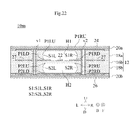
- FIG. 22 is a cross-sectional view of the transmission line 10 m.
- FIG. 23 is a cross-sectional view of the transmission line 10n.
- FIG. 24 is a cross-sectional view of the transmission line 10o.
- FIG. 1 is an exploded perspective view of the transmission line 10.
- reference numerals are given only to the representative interlayer connection conductors v1 and v2 among the plurality of interlayer connection conductors v1 and v2.
- FIG. 2 is a cross-sectional view of the transmission line 10 in AA of FIG.
- the direction is defined as follows.
- the direction in which the normal of the main surface of the prime field 12 of the transmission line 10 extends is defined as the vertical direction of the prime field.
- the direction in which the signal conductor layer 22 of the transmission line 10 extends is defined as the front-back direction of the prime field.
- the line width direction of the signal conductor layer 22 is defined as the left-right direction of the prime field.
- the vertical direction of the prime field, the front-back direction of the prime field, and the left-right direction of the prime field are orthogonal to each other.
- X is a component or member of the transmission line 10. Unless otherwise specified, each part of X is defined as follows in the present specification.
- the front part of X means the front half of X.
- the rear part of X means the rear half of X.
- the left part of X means the left half of X.
- the right part of X means the right half of X.
- the upper part of X means the upper half of X.
- the lower part of X means the lower half of X.
- the front end of X means the front end of X.
- the rear end of X means the rear end of X.
- the left end of X means the left end of X.
- the right end of X means the right end of X.
- the upper end of X means the upper end of X.
- the lower end of X means the lower end of X.
- the front end portion of X means the front end portion of X and its vicinity.
- the rear end portion of X means the rear end portion of X and its vicinity.
- the left end portion of X means the left end portion of X and its vicinity.
- the right end portion of X means the right end portion of X and its vicinity.
- the upper end portion of X means the upper end portion of X and its vicinity.
- the lower end portion of X means the lower end portion of X and its vicinity.
- the transmission line 10 transmits a high frequency signal.
- the transmission line 10 is used in an electronic device such as a smartphone to electrically connect two circuits.
- the transmission line 10 includes a prime field 12, protective layers 20a and 20b, a signal conductor layer 22, a first ground conductor layer 24, a second ground conductor layer 26, a third ground conductor layer 27, and a signal terminal.
- 28a, 28b, a plurality of interlayer connecting conductors v1 and v2, and interlayer connecting conductors v3 and v4 are provided.
- the prime field 12 has a plate shape. Therefore, the prime field 12 has an upper main surface and a lower main surface (main surface). The upper main surface and the lower main surface (main surface) of the prime field 12 have normals extending in the vertical direction of the prime field. The upper and lower main surfaces of the prime field 12 have a rectangular shape having long sides extending in the front-rear direction of the prime field. Therefore, the length of the prime field 12 in the front-back direction of the prime field is longer than the length of the prime field 12 in the left-right direction of the prime field.
- the prime field 12 includes insulator layers 16a to 16c, 18a, and 18b.
- the prime field 12 has a structure in which the insulator layers 16a, 18a, 16b, 18b, 16c are laminated in this order from top to bottom in the vertical direction of the prime field.
- the insulator layers 16a to 16c, 18a, 18b have the same rectangular shape as the prime field 12 when viewed in the vertical direction of the prime field.
- the insulator layers 16a to 16c are flexible dielectric sheets.
- the material of the insulator layers 16a to 16c is, for example, a thermoplastic resin.
- the thermoplastic resin is, for example, a liquid crystal polymer, PTFE (polytetrafluoroethylene) or the like.
- the material of the insulator layers 16a to 16c may be polyimide.
- the insulator layer 18a is an adhesive layer that adheres the insulator layer 16a and the insulator layer 16b.
- the insulator layer 18a is a single-layer insulator layer. The fact that the insulator layer 18a is a single layer means that the insulator layer 18a does not have a structure in which a plurality of insulator layers are bonded together.
- the insulator layer 18b is an adhesive layer that adheres the insulator layer 16b and the insulator layer 16c.
- the insulator layer 18b is a single-layer insulator layer.
- the insulator layer 18b (second insulator layer) is provided below the insulator layer 18a (first insulator layer) in the vertical direction of the prime field.
- “the insulator layer 18b is provided below the insulator layer 18a in the vertical direction of the prime field” refers to the following state.
- the insulator layer 18b is arranged above the prime field in the vertical direction of a plane (upper main surface) that passes through the upper end of the insulator layer 18a and is orthogonal to the vertical direction of the prime field. In this case, the insulator layer 18a and the insulator layer 18b may or may not be arranged in the vertical direction of the prime field.
- the insulator layers 18a and 18b are a sheet having adhesiveness, a liquid adhesive applied by printing or the like, a bonding sheet having viscosity and being attached in a sheet state, and the like.
- the materials of the insulator layers 18a and 18b are, for example, epoxy resin, fluororesin, acrylic resin and the like.
- the material of the insulator layer 18a (first insulator layer) is the insulator layer 16b (third insulator layer) provided below the insulator layer 18a (first insulator layer) in the vertical direction of the element body. It is different from the material of the body layer).
- the signal conductor layer 22 is provided below the insulator layer 18a (first insulator layer) in the prime field 12 in the vertical direction of the prime field. Further, the signal conductor layer 22 is provided above the insulator layer 18b (second insulator layer) in the prime field 12 in the vertical direction of the prime field. In the present embodiment, the signal conductor layer 22 is provided on the upper main surface of the insulator layer 16b. As a result, the signal conductor layer 22 is provided in the prime field 12.
- the signal conductor layer 22 has a linear shape. The signal conductor layer 22 extends in the front-back direction of the prime field. The signal conductor layer 22 is located at the center of the upper main surface of the insulator layer 16b in the left-right direction of the element body.
- the first ground conductor layer 24 is provided above the insulator layer 18a (first insulator layer) in the prime field 12 in the vertical direction of the prime field.
- the first ground conductor layer 24 is provided on the upper main surface of the insulator layer 16a.
- the first ground conductor layer 24 is located above the signal conductor layer 22 in the vertical direction of the element body.
- "the first ground conductor layer 24 is located above the signal conductor layer 22 in the vertical direction of the element body” refers to the following state. At least a part of the first ground conductor layer 24 is arranged in a region through which the signal conductor layer 22 translates in the upward direction of the prime field.
- the first ground conductor layer 24 may be contained in the region through which the signal conductor layer 22 moves in parallel in the upward direction of the prime field, or the signal conductor layer 22 may move in parallel in the upward direction of the prime field. It may sometimes protrude from the area through which it passes.
- the first ground conductor layer 24 covers substantially the entire upper main surface of the insulator layer 16a. Therefore, the first ground conductor layer 24 protrudes from the region through which the signal conductor layer 22 passes when it is translated in the upward direction of the prime field. Further, the first ground conductor layer 24 overlaps with the signal conductor layer 22 when viewed in the vertical direction of the prime field.
- the second ground conductor layer 26 is provided below the insulator layer 18b (second insulator layer) in the prime field 12 in the vertical direction of the prime field.
- the second ground conductor layer 26 is provided on the lower main surface of the insulator layer 16c.
- the second ground conductor layer 26 is located below the signal conductor layer 22 in the vertical direction of the element body.
- the second ground conductor layer 26 covers substantially the entire lower main surface of the insulator layer 16c.
- the second ground conductor layer 26 overlaps with the signal conductor layer 22 when viewed in the vertical direction of the prime field.
- the signal conductor layer 22, the first ground conductor layer 24, and the second ground conductor layer 26 have a stripline structure.
- the third ground conductor layer 27 is provided below the insulator layer 18a (first insulator layer) in the prime field 12 in the vertical direction of the prime field.
- the third ground conductor layer 27 is provided on the upper main surface of the insulator layer 16b.
- the third ground conductor layer 27 surrounds the signal conductor layer 22 when viewed in the vertical direction. Therefore, the third ground conductor layer 27 is provided on the left and right sides of the signal conductor layer 22 in the left-right direction of the element body.
- the plurality of interlayer conductors v1 and v2 electrically connect the first ground conductor layer 24, the second ground conductor layer 26, and the third ground conductor layer 27. More specifically, the plurality of interlayer connecting conductors v1 and v2 penetrate the insulator layers 16a to 16c, 18a, 18b in the vertical direction of the prime field. The upper ends of the plurality of interlayer conductors v1 and v2 are connected to the first ground conductor layer 24. The lower ends of the plurality of interlayer conductors v1 and v2 are connected to the second ground conductor layer 26. The intermediate portions of the plurality of interlayer conductors v1 and v2 are connected to the third ground conductor layer 27.
- the plurality of interlayer connection conductors v1 are provided on the left side of the signal conductor layer 22 in the left-right direction of the element body.
- the plurality of interlayer connecting conductors v1 are arranged in a row at equal intervals in the front-back direction of the prime field.
- the plurality of interlayer connection conductors v2 are provided on the right side of the signal conductor layer 22 in the left-right direction of the element body.
- the plurality of interlayer connecting conductors v2 are arranged in a row at equal intervals in the front-back direction of the prime field.
- the signal terminal 28a is provided on the upper main surface of the prime field 12. More specifically, the signal terminal 28a is provided at the left end of the upper main surface of the insulator layer 16a. The signal terminal 28a overlaps with the left end portion of the signal conductor layer 22 when viewed in the vertical direction of the prime field. However, the signal terminal 28a does not overlap with the first hole H1 and the second hole H2, which will be described later, when viewed in the vertical direction of the prime field. The signal terminal 28a has a rectangular shape when viewed in the vertical direction of the prime field. The first ground conductor layer 24 is not provided around the signal terminal 28a so that the signal terminal 28a is insulated from the first ground conductor layer 24.
- the interlayer connection conductor v3 electrically connects the signal terminal 28a and the signal conductor layer 22. Specifically, the interlayer connecting conductor v3 penetrates the insulator layers 16a and 18a in the vertical direction of the prime field. The upper end of the interlayer connection conductor v3 is connected to the signal terminal 28a. The lower end of the interlayer connection conductor v3 is connected to the left end portion of the signal conductor layer 22. As a result, the signal terminal 28a is electrically connected to the signal conductor layer 22. The high frequency signal is input / output to / from the signal conductor layer 22 via the signal terminal 28a.
- the signal terminal 28b and the interlayer connecting conductor v4 have a symmetrical structure with the signal terminal 28a and the interlayer connecting conductor v3. Therefore, the description of the signal terminal 28b and the interlayer connection conductor v4 will be omitted.
- the signal conductor layer 22, the first ground conductor layer 24, the second ground conductor layer 26, the third ground conductor layer 27, and the signal terminals 28a and 28b as described above are, for example, the upper main surface of the insulator layers 16a to 16c or It is formed by etching a metal foil provided on the lower main surface.
- the metal foil is, for example, a copper foil.
- the interlayer connection conductors v1 to v4 are, for example, through-hole conductors.
- the through-hole conductor is produced by forming through holes in the insulator layers 16a to 16c, 18a, 18b and plating the through holes.
- the protective layers 20a and 20b are flexible insulator layers. However, the protective layers 20a and 20b are not a part of the prime field 12. The protective layers 20a and 20b have the same rectangular shape as the prime field 12 when viewed in the vertical direction of the prime field.
- the protective layer 20a covers substantially the entire upper main surface of the insulator layer 16a. As a result, the protective layer 20a protects the first ground conductor layer 24. However, the protective layer 20a is provided with openings h1 to h6. The opening h1 overlaps with the signal terminal 28a when viewed in the vertical direction of the prime field. As a result, the signal terminal 28a is exposed to the outside from the transmission line 10 through the opening h1.
- the opening h2 is provided on the left side of the opening h1 in the left-right direction of the element body.
- the opening h3 is provided on the right side of the opening h1 in the left-right direction of the element body.
- the first ground conductor layer 24 is exposed to the outside from the transmission line 10 through the openings h2 and h3.
- the structures of the openings h4 to h6 are symmetrical with the structures of the openings h1 to h3, respectively. Therefore, the description of the openings h4 to h6 will be omitted.
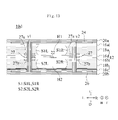
- the insulator layer 18a is provided with a first hole H1 that penetrates the insulator layer 18a in the vertical direction of the prime field. More specifically, as shown in FIG. 1, the first hole H1 has a rectangular shape having a long side extending in the front-back direction of the prime field when viewed in the vertical direction of the prime field. The first hole H1 is provided at the center of the insulator layer 18a in the left-right direction of the element body. As a result, at least a part of the first pore H1 overlaps with the signal conductor layer 22 when viewed in the vertical direction of the prime field.
- the signal conductor layer 22 is located in the first hole H1 as shown in FIG. However, the front end and the rear end of the signal conductor layer 22 do not overlap with the first hole H1 when viewed in the vertical direction of the prime field. That is, the front end and the rear end of the signal conductor layer 22 are not located in the first hole H1.
- the right end portion of the left portion of the third ground conductor layer 27 is located in the first pore H1 as shown in FIG.
- the left end of the right portion of the third ground conductor layer 27 is located in the first hole H1.
- the surface on which the insulator layer 18a forms the first hole H1 is defined as the first hole forming surface S1.
- the first hole forming surface S1 has a left portion S1L and a right portion S1R.
- the left portion S1L of the first pore forming surface S1 has an upper end P1LU and a lower end P1LD.
- the right portion S1R of the first hole forming surface S1 has an upper end P1RU and a lower end P1RD.
- the left portion S1L of the first hole forming surface S1 has an arc shape that protrudes to the left of the prime field when viewed in the front-back direction of the prime field. That is, the left portion S1L of the first vacancy forming surface S1 is the upper end P1LU of the left portion S1L of the first vacancy forming surface S1 and the left portion of the first vacancy forming surface S1 in the cross section orthogonal to the front-back direction of the prime field. It has a curved shape so as to protrude to the left of the prime field from the lower end P1LD of S1L.
- the center of the left portion S1L of the first pore forming surface S1 in the vertical direction of the element body is located on the leftmost side in the left portion S1L.
- the left portion S1L of the first pore forming surface S1 has the upper end P1LU and the first upper end P1LU of the left portion S1L of the first pore forming surface S1 in the cross section orthogonal to the front-back direction of the prime field. It has a portion located to the left in the left-right direction of the prime field from the lower end P1LD of the left portion S1L of the hole forming surface S1.
- the right portion S1R of the first hole forming surface S1 has an arc shape protruding to the right of the prime field when viewed in the front-back direction of the prime field. That is, the right portion S1R of the first vacancy forming surface S1 is the upper end P1RU of the right portion S1R of the first vacancy forming surface S1 and the right portion of the first vacancy forming surface S1 in the cross section orthogonal to the front-back direction of the prime field. It has a curved shape so as to protrude to the right of the prime field from the lower end P1RD of S1R.
- the center of the right portion S1R of the first pore forming surface S1 in the vertical direction of the element body is located on the far right in the right portion S1R.
- the right portion S1R of the first pore forming surface S1 has the upper end P1RU and the first upper end P1RU of the right portion S1R of the first pore forming surface S1 in the cross section orthogonal to the front-back direction of the prime field. It has a portion located to the right in the left-right direction of the prime field from the lower end P1RD of the right portion S1R of the hole forming surface S1.
- the insulator layer 18b is provided with a second hole H2 that penetrates the insulator layer 18b in the vertical direction of the prime field. More specifically, as shown in FIG. 1, the second pore H2 has a rectangular shape having a long side extending in the front-back direction of the prime field when viewed in the vertical direction of the prime field.
- the second hole H2 is provided at the center of the insulator layer 18b in the left-right direction of the element body. As a result, at least a part of the second pore H2 overlaps with the signal conductor layer 22 when viewed in the vertical direction of the prime field. However, the front end and the rear end of the signal conductor layer 22 do not overlap with the second hole H2 when viewed in the vertical direction of the prime field.
- the surface on which the insulator layer 18b forms the second hole H2 is defined as the second hole forming surface S2.
- the second pore forming surface S2 has a left portion S2L and a right portion S2R.
- the left portion S2L of the second pore forming surface S2 has an upper end P2LU and a lower end P2LD.
- the right portion S2R of the second pore forming surface S2 has an upper end P2RU and a lower end P2RD.
- the left portion S2L of the second pore forming surface S2 has an arc shape that protrudes to the left of the prime field when viewed in the front-back direction of the prime field. That is, the left portion S2L of the second vacancy forming surface S2 is the upper end P2LU of the left portion S2L of the second vacancy forming surface S2 and the left portion of the second vacancy forming surface S2 in the cross section orthogonal to the front-back direction of the prime field. It has a curved shape so as to protrude to the left of the prime field from the lower end P2LD of S2L.
- the center of the left portion S2L of the second pore forming surface S2 in the vertical direction of the element body is located on the leftmost side in the left portion S2L.
- the left portion S2L of the second pore forming surface S2 has the upper end P2LU and the second upper end P2LU of the left portion S2L of the second pore forming surface S2 in the cross section orthogonal to the front-back direction of the prime field. It has a portion located to the left in the left-right direction of the prime field from the lower end P2LD of the left portion S2L of the hole forming surface S2.
- the right portion S2R of the second pore forming surface S2 has an arc shape protruding to the right of the prime field when viewed in the front-back direction of the prime field. That is, the right portion S2R of the second pore forming surface S2 is the upper end P2RU of the right portion S2R of the second pore forming surface S2 and the right portion of the second pore forming surface S2 in the cross section orthogonal to the front-back direction of the prime field. It has a curved shape so as to protrude to the right of the prime field from the lower end P2RD of S2R.
- the center of the right portion S2R of the second pore forming surface S2 in the vertical direction of the element body is located on the far right in the right portion S2R.
- the right portion S1R of the second pore forming surface S2 has the upper end P2RU and the second upper end P2RU of the right portion S2R of the second pore forming surface S2 in the cross section orthogonal to the front-back direction of the prime field. It has a portion located to the right in the left-right direction of the prime field from the lower end P2RD of the right portion S2R of the hole forming surface S2.
- the method of forming the first hole H1 and the second hole H2 as described above will be described.
- a method for forming the first hole H1 and the second hole H2 there are a thermal expansion method, a volatilization method and a pressure method.
- the difference between the linear expansion coefficient of the insulator layers 16a to 16c and the linear expansion coefficient of the insulator layers 18a and 18b is used.
- the first pore H1 becomes smaller due to the thermocompression bonding pressure.
- the coefficient of linear expansion of the insulator layers 18a and 18b is larger than the coefficient of linear expansion of the insulator layers 16a to 16c.
- the insulator layers 18a, 18b are larger than the insulator layers 16a to 16c. Shrink.
- the upper main surface of the insulator layer 18a is adhered to the lower main surface of the insulator layer 16a.
- the lower main surface of the insulator layer 18a is adhered to the upper main surface of the insulator layer 16b. Therefore, each of the upper main surface and the lower main surface of the insulator layer 18a is constrained to the lower main surface of the insulator layer 16a and the upper main surface of the insulator layer 16b.
- the left portion S1L of the first pore forming surface S1 is deformed so as to project to the left of the prime field.
- the right portion S1R of the first pore forming surface S1 is deformed so as to project to the right of the prime field.
- the left portion S2L of the second pore forming surface S2 is deformed so as to project to the left of the prime field.
- the right portion S2R of the second pore forming surface S2 is deformed so as to project to the right of the prime field.
- the first hole H1 and the second hole H2 are formed.
- the volatilization method utilizes the fact that the components contained in the insulator layers 18a and 18b are volatilized by thermocompression bonding of the insulator layers 16a to 16c, 18a and 18b. More specifically, when the insulator layers 16a to 16c, 18a, 18b are thermocompression bonded, the first pores H1 and the second pores H2 become smaller due to the thermocompression bonding pressure. Here, the components contained in the insulator layers 18a and 18b are volatilized by thermocompression bonding of the insulator layers 16a to 16c, 18a and 18b.
- the reduction rate of the volumes of the insulator layers 18a and 18b before and after thermocompression bonding is larger than the reduction rate of the volumes of the insulator layers 16a to 16c before and after thermocompression bonding.
- the upper main surface of the insulator layer 18a is adhered to the lower main surface of the insulator layer 16a.
- the lower main surface of the insulator layer 18a is adhered to the upper main surface of the insulator layer 16b. Therefore, each of the upper main surface and the lower main surface of the insulator layer 18a is constrained to the lower main surface of the insulator layer 16a and the upper main surface of the insulator layer 16b.
- the left portion S1L of the first pore forming surface S1 is deformed so as to project to the left of the prime field.
- the right portion S1R of the first pore forming surface S1 is deformed so as to project to the right of the prime field.
- the left portion S2L of the second pore forming surface S2 is deformed so as to project to the left of the prime field.
- the right portion S2R of the second pore forming surface S2 is deformed so as to project to the right of the prime field.
- the first hole H1 and the second hole H2 are formed.
- the pressure method utilizes the expansion of the first pores H1 and the second pores H2 after thermocompression bonding of the insulator layers 16a to 16c, 18a, 18b. More specifically, when the insulator layers 16a to 16c, 18a, 18b are thermocompression bonded, the first pores H1 and the second pores H2 become smaller due to the thermocompression bonding pressure. When the thermocompression bonding of the insulator layers 16a to 16c, 18a, 18b is completed, the pressure applied to the first hole H1 and the second hole H2 becomes smaller, so that the first hole H1 and the second hole H2 become larger. .. However, the upper main surface of the insulator layer 18a is adhered to the lower main surface of the insulator layer 16a.
- the lower main surface of the insulator layer 18a is adhered to the upper main surface of the insulator layer 16b. Therefore, each of the upper main surface and the lower main surface of the insulator layer 18a is constrained to the lower main surface of the insulator layer 16a and the upper main surface of the insulator layer 16b. Therefore, the left portion S1L of the first pore forming surface S1 is deformed so as to project to the left of the prime field. Similarly, the right portion S1R of the first pore forming surface S1 is deformed so as to project to the right of the prime field. Similarly, the left portion S2L of the second pore forming surface S2 is deformed so as to project to the left of the prime field. Similarly, the right portion S2R of the second pore forming surface S2 is deformed so as to project to the right of the prime field. As a result, the first hole H1 and the second hole H2 are formed.
- FIG. 3 is a left side view of the electronic device 1 provided with the transmission line 10.
- the electronic device 1 is, for example, a mobile wireless communication terminal.
- the electronic device 1 is, for example, a smartphone.
- the transmission line 10 is bent as shown in FIG. "The transmission line 10 is bent" means that the transmission line 10 is deformed and bent due to an external force applied to the transmission line 10.
- the section in which the transmission line 10 is bent is referred to as a bending section A2.
- the sections where the transmission line 10 is not bent are called non-bending sections A1 and A3.
- the x-axis, y-axis, and z-axis in the electronic device 1 are defined as follows.
- the x-axis is the anteroposterior direction of the element in the non-bending section A1.
- the y-axis is the left-right direction of the element body in the non-bending section A1.
- the z-axis is the vertical direction of the element body in the non-bending section A1.
- the non-bending section A1, the bending section A2, and the non-bending section A3 are arranged in this order in the positive direction of the x-axis.
- the bending section A2 is bent in the z-axis direction. Therefore, the vertical direction of the prime field and the front-back direction of the prime field differ depending on the position of the transmission line 10, as shown in FIG.
- the non-bending section A1 and the non-bending section A3 for example, the position of (1) in which the prime field 12 is not bent, the vertical direction of the prime field and the front-back direction of the prime field coincide with the z-axis direction and the x-axis direction, respectively. do.
- the vertical direction of the prime field and the front-back direction of the prime field do not coincide with the z-axis direction and the x-axis direction, respectively.
- the electronic device 1 includes a transmission line 10, connectors 30a, 30b, 102a, 102b, and circuit boards 100, 110.
- the circuit boards 100 and 110 have a plate shape.
- the circuit board 100 has main surfaces S5 and S6.
- the main surface S5 is located on the negative direction side of the z-axis with respect to the main surface S6.
- the circuit board 110 has main surfaces S11 and S12.
- the main surface S11 is located on the negative direction side of the z-axis with respect to the main surface S12.
- the circuit boards 100 and 110 include a wiring conductor layer, a ground conductor layer, electrodes and the like (not shown).
- Each of the connectors 30a and 30b is mounted on the main surface (upper main surface) on the positive direction side of the z-axis of the non-bending section A1 and the non-bending section A3. More specifically, the connector 30a is mounted on the signal terminals 28a and the first ground conductor layer 24 exposed from the openings h1 to h3. The connector 30b is mounted on the signal terminals 28b and the first ground conductor layer 24 exposed from the openings h4 to h6.
- Each of the connectors 102a and 102b is mounted on the main surface S5 of the circuit board 100 and the main surface S11 of the circuit board 110.
- Each of the connectors 102a and 102b is connected to the connectors 30a and 30b.
- the transmission line 10 electrically connects the circuit board 100 and the circuit board 110.
- the insulator layer 18a is provided with a first hole H1 that penetrates the insulator layer 18a in the vertical direction of the prime field. Air having a low dielectric constant is present in the first pore H1. At least a part of the first hole H1 overlaps with the signal conductor layer 22 when viewed in the vertical direction of the prime field. Therefore, the dielectric constant around the signal conductor layer 22 becomes low. As a result, in the transmission line 10, it is suppressed that a dielectric loss is generated in the high frequency signal transmitted through the signal conductor layer 22, so that the transmission loss of the transmission line 10 is low.
- the second hole H2 also contributes to the reduction of the transmission loss of the transmission line 10 for the same reason as the first hole H1.
- the transmission loss of the transmission line 10 can be reduced while suppressing the separation between the insulator layer 16a and the insulator layer 18a and the separation between the insulator layer 16b and the insulator layer 18a.
- the upper end P1LU of the left portion S1L of the first pore forming surface S1 is separated from the left surface of the prime field 12. That is, the region where the insulator layer 16a and the insulator layer 18a are adhered becomes wider.
- the lower end P1LD of the left portion S1L of the first pore forming surface S1 is separated from the left surface of the prime field 12. That is, the region where the insulator layer 16b and the insulator layer 18a are adhered becomes wider.
- the peeling of the insulator layer 16a and the insulator layer 18a and the peeling of the insulator layer 16b and the insulator layer 18a are suppressed.
- the left portion S1L of the first vacancy forming surface S1 has an upper end P1LU and a first vacancy of the left portion S1L of the first vacancy forming surface S1 in a cross section orthogonal to the front-back direction of the prime field. It has a portion located to the left in the left-right direction of the prime field from the lower end P1LD of the left portion S1L of the hole forming surface S1.
- the left portion S1L of the first pore forming surface S1 has a shape that protrudes to the left of the prime field in a cross section orthogonal to the front-back direction of the prime field. Therefore, the volume of the first pore H1 is large.
- the transmission line 10 it is suppressed that a dielectric loss is generated in the high frequency signal transmitted through the signal conductor layer 22, so that the transmission loss of the transmission line 10 is low.
- the second hole H2 also suppresses the peeling of the insulator layer 16b and the insulator layer 18b and the peeling of the insulator layer 16c and the insulator layer 18b for the same reason as the first hole H1 and transmits. It contributes to the reduction of the transmission loss of the line 10.
- the right portion S1R of the first pore forming surface S1 has a shape symmetrical with the left portion S1L of the first pore forming surface S1.
- the left portion S1L of the first pore forming surface S1 has a shape protruding to the left of the prime field in a cross section orthogonal to the front-back direction of the prime field.
- the left portion S1L of the first pore forming surface S1 is curved.
- the transmission line 10 since the first hole H1 is provided, the prime field 12 is easily deformed. As a result, the transmission line 10 can be easily bent and used. Also, the amount of adhesive used in the transmission line 10 is reduced. Therefore, the manufacturing cost of the transmission line 10 can be reduced and the weight of the transmission line 10 can be reduced.
- the second vacancies H2, like the first vacancies H1, also contribute to easily deforming the prime field 12 and reducing the amount of adhesive.
- the transmission loss of the transmission line 10 can be reduced for the following reasons. More specifically, an electric field is radiated from the signal conductor layer 22. The electric field tends to pass through the insulator layer 16a having a higher dielectric constant than the first pore H1 having a lower dielectric constant. Therefore, when the insulator layer 16a is present near the signal conductor layer 22, the electric field radiated by the signal conductor layer 22 extends to the left of the prime field and passes through the insulator layer 16a. In this case, on the left side of the signal conductor layer 22, the electric field is concentrated at the corner of the signal conductor layer 22. Such concentration of electric fields causes concentration of current at the corners of the signal conductor layer 22. As a result, the transmission loss of the transmission line 10 may increase.
- the left portion S1L of the first vacancy forming surface S1 has an upper end P1LU and a first vacancy of the left portion S1L of the first vacancy forming surface S1 in a cross section orthogonal to the front-back direction of the prime field. It has a portion located to the left in the left-right direction of the prime field from the lower end P1LD of the left portion S1L of the hole forming surface S1. Therefore, the left portion S1L of the first pore forming surface S1 projects in a direction away from the signal conductor layer 22. As a result, the number of insulator layers 18a located near the signal conductor layer 22 is reduced.
- the electric field radiated by the signal conductor layer 22 spreads in the upper left direction of the prime field.
- the concentration of the electric field at the corner of the signal conductor layer 22 is suppressed.
- the transmission loss of the transmission line 10 can be reduced.
- the first hole H1 is located near the interlayer connecting conductors v1 and v2, it becomes difficult for a capacitance to be formed between the signal conductor layer 22 and the interlayer connecting conductors v1 and v2. As a result, the signal conductor layer 22 and the interlayer connection conductors v1 and v2 can be brought close to each other.
- the first hole H1 is located near the interlayer connecting conductor v1 means, for example, the interlayer connecting conductor located at the left end of the first hole H1 and the left end of the first hole H1 in the left-right direction of the prime field. It means that the distance from v1 is shorter than the distance between the interlayer connection conductor v1 and the signal conductor layer 22.
- the wavelength of the high frequency signal transmitted through the plurality of interlayer connection conductors v1 and v2 becomes longer.
- the spacing between the plurality of interlayer connecting conductors v1 and the spacing between the plurality of interlayer connecting conductors v2 become long.
- Water vapor in the air may oxidize the conductor layer such as the signal line conductor layer 20 and deteriorate the signal characteristics.
- the conductor layer such as the signal line conductor layer 20
- the adsorptivity of unnecessary gas contained in the air in the resin 18a increases, and the water vapor contained in the air decreases.
- deterioration of the characteristics can be suppressed by reducing water vapor and the like in the air.
- the transmission line 10 separation of the insulator layer 16b and the insulator layer 18a is suppressed. More specifically, if the right end of the left portion of the third ground conductor layer 27 is not located in the first hole H1, the right end portion of the left portion of the third ground conductor layer 27 forms the first hole. It is located to the left of the left portion S1L of the surface S1. In this case, a gap is formed between the insulator layer 16b and the insulator layer 18a in the vicinity of the lower end P1LD of the left portion S1L of the first pore forming surface S1. Such a gap causes peeling between the insulator layer 16b and the insulator layer 18a.
- the right end portion of the left portion of the third ground conductor layer 27 is located in the first pore H1. That is, a part of the third ground conductor layer 27 is located in the first hole H1.
- no gap is formed between the insulator layer 16b and the insulator layer 18a in the vicinity of the lower end P1LD of the left portion S1L of the first pore forming surface S1.
- separation of the insulator layer 16b and the insulator layer 18a is suppressed.
- the signal conductor layer 22 is located in the first hole H1 as shown in FIG. As a result, the signal conductor layer 22 comes into contact with air, so that the dielectric constant around the signal conductor layer 22 becomes low. As a result, it is possible to suppress the occurrence of dielectric loss in the high frequency signal transmitted through the signal conductor layer 22.
- the signal terminal 28a does not overlap with the first hole H1 and the second hole H2, which will be described later, when viewed in the vertical direction of the prime field. As a result, it is possible to prevent the transmission line 10 from being damaged by the stress during thermocompression bonding during the manufacture of the transmission line 10.
- FIG. 4 is a cross-sectional view of the transmission line 10a.
- the transmission line 10a is different from the transmission line 10 at the position where the first ground conductor layer 24 and the second ground conductor layer 26 are provided. More specifically, the first ground conductor layer 24 is provided on the lower main surface of the insulator layer 16a. As a result, the first ground conductor layer 24 faces the first pore H1. The second ground conductor layer 26 is provided on the upper main surface of the insulator layer 16c. As a result, the second ground conductor layer 26 faces the second pore H2. Since the other structures of the transmission line 10a are the same as those of the transmission line 10, the description thereof will be omitted. Further, the transmission line 10a can exert the same effect as the transmission line 10.
- FIG. 5 is a cross-sectional view of the transmission line 10b.
- FIG. 6 is a cross-sectional view of the transmission line 500 according to the comparative example.
- the transmission line 10b is different from the transmission line 10 in that it does not include the insulator layers 16a and 16c, the protective layers 20a and 20b, and the interlayer connection conductors v1 and v2. As described above, the insulator layers 16a and 16c, the protective layers 20a and 20b, and the interlayer connection conductors v1 and v2 are not essential configurations.
- the first ground conductor layer 24 is attached to the upper main surface of the insulator layer 18a by, for example, a transfer method.
- the second ground conductor layer 26 is attached to the lower main surface of the insulator layer 18b by, for example, a transfer method. Since the other structures of the transmission line 10b are the same as those of the transmission line 10, the description thereof will be omitted. Further, the transmission line 10b can exert the same effect as the transmission line 10.
- the inventor of the present application performed the computer simulation described below in order to clarify the effect of the transmission line 10b. Specifically, a first model having the structure of the transmission line 10b and a second model having the structure of the transmission line 500 were created. The difference between the first model and the second model is the shape of the first hole H1 and the second hole H2. The distance L1 between the upper end P1LU and the upper end P1RU in the first model is equal to the distance L2 between the upper end P1LU and the upper end P1RU in the second model.
- the inventor of the present application has a computer calculate the distribution of the electric field around the signal conductor layer 22 using the first model and the second model.
- the inventor of the present application has a computer calculate the relationship between the frequencies of the first model and the second model and the transmission loss of the first model and the second model. At this time, the inventor of the present application calculated under the condition that the first ground conductor layer 24 and the second ground conductor layer 26 were electrically connected and a high frequency signal was applied between the first ground conductor layer 24 and the signal conductor layer 22.
- FIG. 7 is a diagram showing the electric field distribution of the first model.
- FIG. 8 is a diagram showing the electric field distribution of the second model.
- a dark-colored portion means a portion having a high electric field strength
- a light-colored portion means a portion having a low electric field strength. Comparing FIGS. 7 and 8, it can be seen that the region where the electric field strength is low in the first model is wider than the region where the electric field strength is low in the second model. Further, it can be seen that the strength of the electric field of the insulator layer, which has a larger dielectric loss than air, is smaller in the first model than in the second model.
- the volume of the first hole H1 and the second hole H2 of the first model is larger than the volume of the first hole H1 and the second hole H2 of the second model.
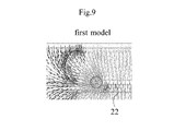
- FIG. 9 is a diagram showing the electric field distribution at the left end portion of the signal conductor layer 22 of the first model.
- FIG. 10 is a diagram showing an electric field distribution at the left end portion of the signal conductor layer 22 of the second model. Comparing FIGS. 9 and 10, it can be seen that the first model suppresses the concentration of the electric field at the corners of the signal conductor layer 22 as compared with the second model. As a result, in the first model, the concentration of current at the corner of the signal conductor layer 22 is suppressed. As a result, in the first model, the transmission loss of the high frequency signal is reduced as compared with the second model.
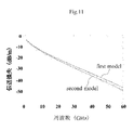
- FIG. 11 is a graph showing the relationship between the frequencies of the first model and the second model and the transmission loss of the first model and the second model.
- the horizontal axis is the frequency of the high frequency signal transmitted through the signal conductor layer 22.
- the vertical axis is the transmission loss of the transmission line per meter of the first model and the second model. According to FIG. 11, it can be seen that the transmission loss of the first model (transmission line 10a) is smaller than the transmission loss of the second model (transmission line 500).
- FIG. 12 is a cross-sectional view of the transmission line 10c.
- the transmission line 10c is different from the transmission line 10a in that the insulator layer 16d and the third ground conductor layers 27a and 27b are further provided. More specifically, the insulator layer 16d is provided between the insulator layer 18a and the insulator layer 16b. As a result, the signal conductor layer 22 is located between the insulator layer 16d and the insulator layer 16b. That is, the signal conductor layer 22 is not located in the first hole H1. As described above, by surrounding the signal conductor layer 22 with the insulator layers 16b and 16d, it is possible to prevent the signal conductor layer 22 from short-circuiting with other conductor layers. Further, deterioration of the signal conductor layer 22 due to oxidation or the like is suppressed.
- the third ground conductor layer 27a is provided on the upper main surface of the insulator layer 16b.
- the third ground conductor layer 27b is provided on the lower main surface of the insulator layer 16d. Since the other structures of the transmission line 10c are the same as those of the transmission line 10a, the description thereof will be omitted.
- the transmission line 10c can exert the same effect as the transmission line 10.
- the third ground conductor layer 27a is located above the signal conductor layer 22 in the vertical direction of the prime field, and the third ground conductor layer 27b is located below the signal conductor layer 22 in the vertical direction of the prime field. This improves the shielding property against the signal conductor layer 22.
- FIG. 13 is a cross-sectional view of the transmission line 10d.
- the transmission line 10d is different from the transmission line 10c at the position where the first ground conductor layer 24 and the second ground conductor layer 26 are provided. More specifically, the first ground conductor layer 24 is provided on the upper main surface of the insulator layer 16a. The second ground conductor layer 26 is provided on the lower main surface of the insulator layer 16c. Since the other structures of the transmission line 10d are the same as those of the transmission line 10c, the description thereof will be omitted. Further, the transmission line 10d can exert the same effect as the transmission line 10c.
- FIG. 14 is a cross-sectional view of the transmission line 10e.
- the transmission line 10e is different from the transmission line 10 in the thickness of the insulator layers 16a, 16c, 18a, 18b and the presence or absence of the holes H3 and H4. More specifically, in the transmission line 10e, the thickness of the insulator layers 18a and 18b is smaller than the thickness of the insulator layers 16a and 16c. Further, the holes H3 and H4 are provided in the insulator layers 16a and 16c, respectively. Each of the holes H3 and H4 penetrates the insulator layers 16a and 16c in the vertical direction of the prime field. Further, the hole H3 is connected to the first hole H1. The hole H4 is connected to the second hole H2. Since the other structures of the transmission line 10e are the same as those of the transmission line 10, the description thereof will be omitted.
- the insulator layers 18a and 18b are adhesive layers. Therefore, the thicknesses of the insulator layers 18a and 18b are likely to change when the prime field 12 is crimped. Therefore, the thickness of the insulator layers 18a and 18b is smaller than the thickness of the insulator layers 16a and 16b. The amount of change in the thickness of the insulator layers 18a and 18b at the time of crimping the prime field 12 is reduced. As a result, it is possible to prevent variations in the sizes of the first hole H1 and the second hole H2 in the vertical direction of the element body.
- FIG. 15 is a cross-sectional view of the transmission line 10f.
- the transmission line 10f is different from the transmission line 10e in that the first hole H11, the second hole H12, and the holes H13, H14 are provided in the prime field 12. More specifically, the first holes H1, the second holes H2, and the holes H3 and H4 are arranged to the left of the center of the prime field 12 in the left-right direction of the prime field. Further, the first holes H11, the second holes H12, and the holes H13, H14 are arranged to the right of the center of the prime field 12 in the left-right direction of the prime field. Each of the first hole H11, the second hole H12, and the holes H13, H14 has a symmetrical structure with the first hole H1, the second hole H2, and the holes H3, H4. Since the other structures of the transmission line 10f are the same as those of the transmission line 10e, the description thereof will be omitted. Further, the transmission line 10f can exert the same effect as the transmission line 10e.
- a part of the insulator layers 16a to 16c, 18a, 18b is a first hole H1, a second hole H2, a hole H3, H4, a first hole H11, and a second hole. It exists between H12 and the holes H13 and H14. As a result, a part of the insulator layers 16a to 16c, 18a, 18b functions as a support. As a result, when the transmission line 10f is bent, the first holes H1, H11, the second holes H2, H12, and the holes H3, H4, H13, H14 are suppressed from being deformed.
- FIG. 16 is a cross-sectional view of the transmission line 10 g.
- the transmission line 10g is different from the transmission line 10f in that the first hole H21, the second hole H22, and the holes H23, H24 are provided in the prime field 12. More specifically, the first hole H21, the second hole H22, and the holes H23, H24 are arranged to the right of the first hole H1, the second hole H2, and the holes H3, H4 in the left-right direction of the prime field. Has been done. The first hole H21, the second hole H22, and the holes H23, H24 are arranged on the left side of the first hole H11, the second hole H12, and the holes H13, H14 in the left-right direction of the prime field.
- Each of the first hole H21, the second hole H22, and the holes H23, H24 has the same structure as the first hole H1, the second hole H2, and the holes H3, H4. Since the other structure of the transmission line 10g is the same as that of the transmission line 10f, the description thereof will be omitted. Further, the transmission line 10g can exert the same effect as the transmission line 10f.
- the insulator layer 16a is located between the first hole H1, the second hole H2 and the hole H3, H4 and the first hole H21, the second hole H22 and the hole H23, H24.
- a part of ⁇ 16c, 18a, 18b is present.
- the insulator layers 16a to 16c, 18a, 18b between the first hole H11, the second hole H12 and the hole H13, H14 and the first hole H21, the second hole H22 and the hole H23, H24. Some exist.
- a part of the insulator layers 16a to 16c, 18a, 18b functions as a support.
- the first holes H1, H11, H21, the second holes H2, H12, H22 and the holes H3, H4, H13, H14, H23, H24 are deformed. Is suppressed.
- FIG. 17 is a cross-sectional view of the transmission line 10h.
- the transmission line 10h is different from the transmission line 10e in that the insulator layers 18c and 18d are further provided, and that the first hole H31 and the second hole H41 are provided in the prime field 12.
- the insulator layer 18c is provided above the insulator layer 16a in the vertical direction of the element body. Therefore, the first ground conductor layer 24 is provided on the upper main surface of the insulator layer 18c.
- the insulator layer 18d is provided below the insulator layer 16c in the vertical direction of the element body. Therefore, the second ground conductor layer 26 is provided on the lower main surface of the insulator layer 18d.
- the first hole H31 penetrates the insulator layer 18c in the vertical direction of the prime field.
- the shape of the first hole H31 is the same as that of the first hole H1.
- the first hole H31 is connected to the hole H3.
- the second hole H41 penetrates the insulator layer 18d in the vertical direction of the prime field.
- the shape of the second hole H41 is the same as that of the first hole H1.
- the second hole H41 is connected to the hole H4. Since the other structures of the transmission line 10h are the same as those of the transmission line 10e, the description thereof will be omitted. Further, the transmission line 10h can exert the same effect as the transmission line 10e.
- the insulator layers 18a to 18d are adhesive layers. Therefore, the thicknesses of the insulator layers 18a to 18d are likely to change when the prime field 12 is crimped. Therefore, the thickness of the insulator layers 18a to 18d is smaller than the thickness of the insulator layers 16a and 16b. The amount of change in the thickness of the insulator layers 18a to 18d at the time of crimping the prime field 12 is reduced. As a result, it is possible to prevent variations in the sizes of the first holes H1, H31, the second holes H2, H41, and the holes H3, H4 in the vertical direction of the element body.
- the transmission loss of the transmission line 10h can be reduced.
- FIG. 18 is a cross-sectional view of the transmission line 10i.
- the transmission line 10i is different from the transmission line 10c in that it includes a plurality of conductors 200 instead of the interlayer connection conductors v1 and v2. More specifically, the plurality of conductors 200 are, for example, metal spheres whose surface is covered with solder or a conductive adhesive. The diameters of the metal spheres of the plurality of conductors 200 are uniform. The plurality of conductors 200 are provided on the insulator layer 18a (first insulator layer). The plurality of conductors 200 electrically connect the first ground conductor layer 24 and the third ground conductor layer 27a.
- the plurality of conductors 200 are provided on the insulator layer 18b.
- the plurality of conductors 200 electrically connect the second ground conductor layer 26 and the third ground conductor layer 27b.
- the plurality of conductors 200 are joined to the second ground conductor layer 26 and the third ground conductor layer 27b. Since the other structures of the transmission line 10i are the same as those of the transmission line 10c, the description thereof will be omitted. Further, the transmission line 10i can exert the same effect as the transmission line 10c.
- the interlayer connection conductors v1 and v2 are not required. Therefore, the plating step for forming the interlayer connection conductors v1 and v2 becomes unnecessary. Therefore, the plating solution does not enter the transmission line 10i.
- the distance between the insulator layer 16a and the insulator layer 16d is substantially determined by the diameters of the metal spheres of the plurality of conductors 200.
- the distance between the insulator layer 16b and the insulator layer 16c is substantially determined by the diameters of the metal spheres of the plurality of conductors 200.
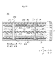
- FIG. 19 is a cross-sectional view of the transmission line 10j.
- the transmission line 10j is different from the transmission line 10c in that the insulator layers 16e and 16f and the conductor layers 150, 152, 160 and 162 are further provided. More specifically, the insulator layer 16e is provided above the insulator layer 16a in the vertical direction of the element body. The insulator layer 16f is provided below the insulator layer 16c in the vertical direction of the element body. The conductor layer 150 is provided on the lower main surface of the insulator layer 16e. The conductor layer 152 is provided on the upper main surface of the insulator layer 16e. The conductor layer 160 is provided on the upper main surface of the insulator layer 16f. The conductor layer 162 is provided on the lower main surface of the insulator layer 16f.
- the conductor layers 150, 152, 160, 162 are signal wirings and ground conductors. By providing the conductor layers 150, 152, 160, 162 in this way, an electric circuit is added to the transmission line 10j. Since the other structures of the transmission line 10j are the same as those of the transmission line 10c, the description thereof will be omitted. Further, the transmission line 10j can exert the same effect as the transmission line 10c.
- FIG. 20 is a cross-sectional view of the transmission line 10k.
- the transmission line 10k is different from the transmission line 10j in that it includes a plurality of conductors 200 instead of the interlayer connection conductors v1 and v2. More specifically, the diameters of the plurality of conductors 200 are uniform.
- the plurality of conductors 200 are provided on the insulator layer 18a (first insulator layer). The plurality of conductors 200 electrically connect the first ground conductor layer 24 and the third ground conductor layer 27a.
- the plurality of conductors 200 are provided on the insulator layer 18b.
- the plurality of conductors 200 electrically connect the second ground conductor layer 26 and the third ground conductor layer 27b. Since the other structures of the transmission line 10k are the same as those of the transmission line 10j, the description thereof will be omitted. Further, the transmission line 10k can exert the same effect as the transmission line 10j.
- FIG. 21 is a cross-sectional view of the transmission line 10l.
- the transmission line 10l does not have the insulator layers 16a and 16c, the material of the insulator layer 16b is the same as the material of the insulator layers 18a and 18b, and the interlayer connection conductors v1 and v2 are via hole conductors. Is different from the transmission line 10. More specifically, the insulator layer 16b (third insulator layer) is provided below the insulator layer 18a (first insulator layer) in the vertical direction of the element body. The material of the insulator layer 16b (third insulator layer) is the same as the material of the insulator layers 18a and 18b (first insulator layer). The material of the insulator layers 16b, 18a, 18b is a thermoplastic resin such as polyimide, a liquid crystal polymer, or PTFE (polytetrafluoroethylene).
- PTFE polytetrafluoroethylene
- the first ground conductor layer 24 is provided on the upper main surface of the insulator layer 18a.
- the second ground conductor layer 26 is provided on the lower main surface of the insulator layer 18b.
- the interlayer connection conductors v1 and v2 electrically connect the first ground conductor layer 24 and the second ground conductor layer 26.
- the interlayer connection conductors v1 and v2 are via hole conductors.
- the via hole conductor is produced by forming through holes in the insulator layers 16b, 18a, 18b, filling the through holes with the conductive paste, and then sintering the conductive paste. Since the other structures of the transmission line 10l are the same as those of the transmission line 10, the description thereof will be omitted. Further, the transmission line 10l can exert the same effect as the transmission line 10.
- an adhesive layer may be used to join a plurality of insulator layers.
- the adhesive layer since the adhesive layer is required to have high adhesiveness, it may be difficult to use a material having a low dielectric constant or a low dielectric loss tangent for the adhesive layer. Therefore, in the transmission line 10l, the material of the insulator layers 18a and 18b is the same thermoplastic resin as the material of the insulator layer 16b. Therefore, the insulator layers 18a, 16b, 18b can be joined by thermocompression bonding. This eliminates the need for an adhesive layer for joining the insulator layers. As a result, in the transmission line 10l, the transmission loss of the transmission line 10l can be reduced.
- the material of the insulator layer 16b is the same as the material of the insulator layers 18a and 18b. Therefore, the coefficient of linear expansion of the insulator layer 16b is equal to the coefficient of linear expansion of the insulator layers 18a and 18b. As a result, when the temperature of the transmission line 10l changes, stress may be generated inside the prime field 12 due to the difference between the linear expansion coefficient of the insulator layer 16b and the linear expansion coefficient of the insulator layers 18a and 18b. It is suppressed.
- the interlayer connection conductors v1 and v2 which are via hole conductors, at the time of thermocompression bonding of the prime field 12.
- FIG. 22 is a cross-sectional view of the transmission line 10 m.
- the transmission line 10m is different from the transmission line 10l in that the interlayer connection conductors v1 and v2 are through-hole conductors. Since the other structure of the transmission line 10m is the same as that of the transmission line 10l, the description thereof will be omitted. Further, the transmission line 10m can exert the same effect as the transmission line 10l.
- FIG. 23 is a cross-sectional view of the transmission line 10n.
- the transmission line 10n is different from the transmission line 10 in that the second hole H2 is not provided. Since the other structures of the transmission line 10n are the same as those of the transmission line 10, the description thereof will be omitted. Further, the transmission line 10n can exert the same effect as that of the transmission line 10. It should be noted that the second hole H2 may not be provided even in the transmission lines 10a to 10m.
- FIG. 24 is a cross-sectional view of the transmission line 10o.
- the transmission line 10o is different from the transmission line 10 in that the signal conductor layers 22a and 22b are further provided.
- the signal conductor layer 22a is provided on the left side of the signal conductor layer 22 in the left-right direction of the element body.
- the signal conductor layer 22b is provided on the right side of the signal conductor layer 22 in the left-right direction of the element body. Since the other structures of the transmission line 10o are the same as those of the transmission line 10, the description thereof will be omitted. Further, the transmission line 10o can exert the same effect as the transmission line 10.
- the transmission line 10o may be provided with two signal conductor layers, or may be provided with four or more signal conductor layers. Further, two adjacent signal conductor layers among the plurality of signal conductor layers may form a differential transmission line.
- the transmission lines 10a to 10m may further include signal conductor layers 22a and 22b.
- the transmission line according to the present invention is not limited to the transmission lines 10, 10a to 10o, and can be changed within the scope of the gist thereof.
- the configurations of the transmission lines 10, 10a to 10o may be arbitrarily combined.
- the left portion S1L of the first hole forming surface S1 does not need to have a portion located to the left of the upper end P1LU and the lower end P1LD in the left-right direction of the prime field. .. Therefore, in a part of the cross section of the transmission lines 10, 10a to 10o, the left portion S1L of the first hole forming surface S1 may have a portion located to the left of the upper end P1LU and the lower end P1LD in the left-right direction of the prime field. Just do it.
- the right portion S1R of the first hole forming surface S1 does not need to have a portion located to the right of the upper end P1RU and the lower end P1RD in the left-right direction of the prime field. .. Therefore, in a part of the cross section of the transmission lines 10, 10a to 10o, the right portion S1R of the first hole forming surface S1 may have a portion located to the right of the upper end P1RU and the lower end P1RD in the left-right direction of the prime field. Just do it.
- the second ground conductor layer 26 is not an essential configuration. Further, since the transmission line 10 does not include the second ground conductor layer 26, the insulator layers 18b, 16c and the protective layer 20b, the signal conductor layer 22 and the first ground conductor layer 24 have a microstrip line structure. You may.
- the right portion S1R of the first hole forming surface S1 is a portion located to the right of the upper end P1RU and the lower end P1RD in the left-right direction of the prime field in the cross section orthogonal to the front-back direction of the prime field. You do not have to have.
- the insulator layer 16a and the insulator layer 18a are more curved than when either the left portion S1L or the right portion S1R is curved.
- the peeling of the insulator layer 16b and the insulator layer 18a can be effectively suppressed, and the transmission loss of the transmission line 10 can be effectively reduced.
- the insulator layer 18a may be an anisotropic conductive film.
- the plurality of conductors 200 are fine metal particles of the anisotropic conductive film.
- the signal terminals 28a and 28b may be provided on the lower main surface of the prime field 12.
- the transmission lines 10, 10a to 10o may further include other circuits in addition to the stripline lines.
- the transmission lines 10, 10a to 10o have a linear shape when viewed in the vertical direction of the prime field. However, the transmission lines 10, 10a to 10o may be bent. Here, “the transmission lines 10, 10a to 10o are bent” means that the transmission lines 10, 10a to 10o have a bent shape without applying an external force.
- the first hole H1 and the second hole H2 are provided in the non-bent sections A1 and A3, and may not be provided in the bent section A2.
- the right portion S1R of the first hole forming surface S1 may have a shape that is not symmetrical with the left portion S1L of the first hole forming surface S1.
- the right portion S1R of the first hole forming surface S1 is the left portion of the first hole forming surface S1. It has a shape that is not symmetrical with S1L. In such a case, the one closer to the signal conductor layer 22 in the left portion S1L and the right portion S1R may be curved.
- the one closer to the signal conductor layer 22 in the left portion S1L and the right portion S1R may be curved more than the far side to the signal conductor layer 22 in the right portion S1R and the left portion S1L.
- the width in the left-right direction of the left portion S1L or the width in the left-right direction of the right portion S1R may be smaller than the thickness in the vertical direction of the transmission line 10.
Landscapes
- Engineering & Computer Science (AREA)
- Microelectronics & Electronic Packaging (AREA)
- Structure Of Printed Boards (AREA)
- Waveguides (AREA)
- Production Of Multi-Layered Print Wiring Board (AREA)
Priority Applications (5)
| Application Number | Priority Date | Filing Date | Title |
|---|---|---|---|
| CN202190000821.9U CN220066075U (zh) | 2020-11-30 | 2021-10-22 | 传输线路以及电子设备 |
| JP2022565123A JP7327690B2 (ja) | 2020-11-30 | 2021-10-22 | 伝送線路及び電子機器 |
| US18/201,211 US12394876B2 (en) | 2020-11-30 | 2023-05-24 | Transmission line and electronic device |
| JP2023124127A JP7772040B2 (ja) | 2020-11-30 | 2023-07-31 | 伝送線路 |
| US19/266,286 US20250343341A1 (en) | 2020-11-30 | 2025-07-11 | Transmission line and electronic device |
Applications Claiming Priority (2)
| Application Number | Priority Date | Filing Date | Title |
|---|---|---|---|
| JP2020198382 | 2020-11-30 | ||
| JP2020-198382 | 2020-11-30 |
Related Child Applications (1)
| Application Number | Title | Priority Date | Filing Date |
|---|---|---|---|
| US18/201,211 Continuation US12394876B2 (en) | 2020-11-30 | 2023-05-24 | Transmission line and electronic device |
Publications (1)
| Publication Number | Publication Date |
|---|---|
| WO2022113591A1 true WO2022113591A1 (ja) | 2022-06-02 |
Family
ID=81754259
Family Applications (1)
| Application Number | Title | Priority Date | Filing Date |
|---|---|---|---|
| PCT/JP2021/039061 Ceased WO2022113591A1 (ja) | 2020-11-30 | 2021-10-22 | 伝送線路及び電子機器 |
Country Status (4)
| Country | Link |
|---|---|
| US (2) | US12394876B2 (https=) |
| JP (2) | JP7327690B2 (https=) |
| CN (2) | CN221304960U (https=) |
| WO (1) | WO2022113591A1 (https=) |
Cited By (6)
| Publication number | Priority date | Publication date | Assignee | Title |
|---|---|---|---|---|
| JPWO2022260094A1 (https=) * | 2021-06-09 | 2022-12-15 | ||
| WO2025121070A1 (ja) * | 2023-12-06 | 2025-06-12 | 株式会社村田製作所 | 高周波信号伝送線路及び電子機器 |
| WO2025121071A1 (ja) * | 2023-12-06 | 2025-06-12 | 株式会社村田製作所 | 高周波信号伝送線路及び電子機器 |
| WO2025121069A1 (ja) * | 2023-12-06 | 2025-06-12 | 株式会社村田製作所 | 高周波信号伝送線路及び電子機器 |
| WO2026048712A1 (ja) * | 2024-08-29 | 2026-03-05 | 株式会社村田製作所 | 伝送線路及び電子機器 |
| WO2026048599A1 (ja) * | 2024-09-02 | 2026-03-05 | 株式会社村田製作所 | 多層基板及び電子機器 |
Citations (2)
| Publication number | Priority date | Publication date | Assignee | Title |
|---|---|---|---|---|
| JP2002151854A (ja) * | 2000-11-15 | 2002-05-24 | Genesis Technology Kk | 多層プリント配線板およびその製造方法 |
| WO2017130731A1 (ja) * | 2016-01-27 | 2017-08-03 | 株式会社村田製作所 | 信号伝送線路 |
Family Cites Families (4)
| Publication number | Priority date | Publication date | Assignee | Title |
|---|---|---|---|---|
| US5712607A (en) * | 1996-04-12 | 1998-01-27 | Dittmer; Timothy W. | Air-dielectric stripline |
| TWI445249B (zh) | 2010-07-08 | 2014-07-11 | Kuo Chih Hung | 天線模組 |
| JP6285638B2 (ja) | 2013-04-25 | 2018-02-28 | 日本メクトロン株式会社 | プリント配線板およびプリント配線板製造方法 |
| US20170271734A1 (en) | 2016-03-17 | 2017-09-21 | Multek Technologies Limited | Embedded cavity in printed circuit board by solder mask dam |
-
2021
- 2021-10-22 WO PCT/JP2021/039061 patent/WO2022113591A1/ja not_active Ceased
- 2021-10-22 CN CN202323086718.0U patent/CN221304960U/zh active Active
- 2021-10-22 JP JP2022565123A patent/JP7327690B2/ja active Active
- 2021-10-22 CN CN202190000821.9U patent/CN220066075U/zh active Active
-
2023
- 2023-05-24 US US18/201,211 patent/US12394876B2/en active Active
- 2023-07-31 JP JP2023124127A patent/JP7772040B2/ja active Active
-
2025
- 2025-07-11 US US19/266,286 patent/US20250343341A1/en active Pending
Patent Citations (2)
| Publication number | Priority date | Publication date | Assignee | Title |
|---|---|---|---|---|
| JP2002151854A (ja) * | 2000-11-15 | 2002-05-24 | Genesis Technology Kk | 多層プリント配線板およびその製造方法 |
| WO2017130731A1 (ja) * | 2016-01-27 | 2017-08-03 | 株式会社村田製作所 | 信号伝送線路 |
Cited By (10)
| Publication number | Priority date | Publication date | Assignee | Title |
|---|---|---|---|---|
| JPWO2022260094A1 (https=) * | 2021-06-09 | 2022-12-15 | ||
| WO2022260094A1 (ja) * | 2021-06-09 | 2022-12-15 | 株式会社村田製作所 | 導体層付き樹脂フィルム、積層基板、及び、導体層付き樹脂フィルムの製造方法 |
| US12330392B2 (en) | 2021-06-09 | 2025-06-17 | Murata Manufacturing Co., Ltd. | Liquid crystal polymer film, liquid crystal polymer film with conductor layer, and multilayer substrate |
| JP7722451B2 (ja) | 2021-06-09 | 2025-08-13 | 株式会社村田製作所 | 導体層付き樹脂フィルム、積層基板、及び、導体層付き樹脂フィルムの製造方法 |
| US12507340B2 (en) | 2021-06-09 | 2025-12-23 | Murata Manufacturing Co., Ltd. | Resin film with conductor layer, multilayer substrate, and method for producing resin film with conductor layer |
| WO2025121070A1 (ja) * | 2023-12-06 | 2025-06-12 | 株式会社村田製作所 | 高周波信号伝送線路及び電子機器 |
| WO2025121071A1 (ja) * | 2023-12-06 | 2025-06-12 | 株式会社村田製作所 | 高周波信号伝送線路及び電子機器 |
| WO2025121069A1 (ja) * | 2023-12-06 | 2025-06-12 | 株式会社村田製作所 | 高周波信号伝送線路及び電子機器 |
| WO2026048712A1 (ja) * | 2024-08-29 | 2026-03-05 | 株式会社村田製作所 | 伝送線路及び電子機器 |
| WO2026048599A1 (ja) * | 2024-09-02 | 2026-03-05 | 株式会社村田製作所 | 多層基板及び電子機器 |
Also Published As
| Publication number | Publication date |
|---|---|
| US20250343341A1 (en) | 2025-11-06 |
| JP7327690B2 (ja) | 2023-08-16 |
| JPWO2022113591A1 (https=) | 2022-06-02 |
| CN221304960U (zh) | 2024-07-09 |
| JP7772040B2 (ja) | 2025-11-18 |
| JP2023138604A (ja) | 2023-10-02 |
| US20230327309A1 (en) | 2023-10-12 |
| CN220066075U (zh) | 2023-11-21 |
| US12394876B2 (en) | 2025-08-19 |
Similar Documents
| Publication | Publication Date | Title |
|---|---|---|
| WO2022113591A1 (ja) | 伝送線路及び電子機器 | |
| JP6540847B2 (ja) | 伝送線路および電子機器 | |
| CN104396097B (zh) | 电缆的连接、固定方法 | |
| CN205081202U (zh) | 传输线路及扁平电缆 | |
| US12438247B2 (en) | Transmission line and electronic device | |
| US9401533B2 (en) | Flat cable | |
| US20230291086A1 (en) | Transmission line and electronic device | |
| CN103733426B (zh) | 高频信号线路及电子设备 | |
| CN204538168U (zh) | 高频信号线路 | |
| US20210273361A1 (en) | Electronic device and flat cable | |
| US9583809B2 (en) | High-frequency signal line | |
| CN219626872U (zh) | 多层基板 | |
| JP7355256B2 (ja) | 伝送線路及び電子機器 | |
| CN220272720U (zh) | 传输线路以及电子设备 | |
| CN206236772U (zh) | 传输线路构件 | |
| US12438246B2 (en) | Transmission line and electronic device | |
| JP2014175829A (ja) | 伝送線路、アンテナ装置及び伝送線路製造方法 | |
| CN220306489U (zh) | 传输线路以及电子设备 | |
| WO2022270294A1 (ja) | 多層基板、多層基板モジュール及び電子機器 | |
| WO2024171659A1 (ja) | 多層基板、電子機器及び多層基板の製造方法 | |
| WO2022149450A1 (ja) | 多層基板、電子機器及び多層基板の製造方法 | |
| WO2022113739A1 (ja) | 伝送線路及び電子機器 | |
| US9583810B2 (en) | High-frequency signal line |
Legal Events
| Date | Code | Title | Description |
|---|---|---|---|
| 121 | Ep: the epo has been informed by wipo that ep was designated in this application |
Ref document number: 21897569 Country of ref document: EP Kind code of ref document: A1 |
|
| ENP | Entry into the national phase |
Ref document number: 2022565123 Country of ref document: JP Kind code of ref document: A |
|
| WWE | Wipo information: entry into national phase |
Ref document number: 202190000821.9 Country of ref document: CN |
|
| NENP | Non-entry into the national phase |
Ref country code: DE |
|
| 122 | Ep: pct application non-entry in european phase |
Ref document number: 21897569 Country of ref document: EP Kind code of ref document: A1 |