WO2022113174A1 - 光モジュール - Google Patents
光モジュール Download PDFInfo
- Publication number
- WO2022113174A1 WO2022113174A1 PCT/JP2020/043684 JP2020043684W WO2022113174A1 WO 2022113174 A1 WO2022113174 A1 WO 2022113174A1 JP 2020043684 W JP2020043684 W JP 2020043684W WO 2022113174 A1 WO2022113174 A1 WO 2022113174A1
- Authority
- WO
- WIPO (PCT)
- Prior art keywords
- pin
- stem
- hole
- ground
- plane
- Prior art date
- Legal status (The legal status is an assumption and is not a legal conclusion. Google has not performed a legal analysis and makes no representation as to the accuracy of the status listed.)
- Ceased
Links
Images


Classifications
-
- H—ELECTRICITY
- H05—ELECTRIC TECHNIQUES NOT OTHERWISE PROVIDED FOR
- H05K—PRINTED CIRCUITS; CASINGS OR CONSTRUCTIONAL DETAILS OF ELECTRIC APPARATUS; MANUFACTURE OF ASSEMBLAGES OF ELECTRICAL COMPONENTS
- H05K1/00—Printed circuits
- H05K1/18—Printed circuits structurally associated with non-printed electric components
- H05K1/189—Printed circuits structurally associated with non-printed electric components characterised by the use of flexible or folded printed circuits
-
- H—ELECTRICITY
- H05—ELECTRIC TECHNIQUES NOT OTHERWISE PROVIDED FOR
- H05K—PRINTED CIRCUITS; CASINGS OR CONSTRUCTIONAL DETAILS OF ELECTRIC APPARATUS; MANUFACTURE OF ASSEMBLAGES OF ELECTRICAL COMPONENTS
- H05K1/00—Printed circuits
- H05K1/02—Details
- H05K1/0213—Electrical arrangements not otherwise provided for
- H05K1/0216—Reduction of cross-talk, noise or electromagnetic interference
- H05K1/0218—Reduction of cross-talk, noise or electromagnetic interference by printed shielding conductors, ground planes or power plane
-
- H—ELECTRICITY
- H05—ELECTRIC TECHNIQUES NOT OTHERWISE PROVIDED FOR
- H05K—PRINTED CIRCUITS; CASINGS OR CONSTRUCTIONAL DETAILS OF ELECTRIC APPARATUS; MANUFACTURE OF ASSEMBLAGES OF ELECTRICAL COMPONENTS
- H05K1/00—Printed circuits
- H05K1/02—Details
- H05K1/11—Printed elements for providing electric connections to or between printed circuits
- H05K1/118—Printed elements for providing electric connections to or between printed circuits specially for flexible printed circuits, e.g. using folded portions
-
- H—ELECTRICITY
- H01—ELECTRIC ELEMENTS
- H01S—DEVICES USING THE PROCESS OF LIGHT AMPLIFICATION BY STIMULATED EMISSION OF RADIATION [LASER] TO AMPLIFY OR GENERATE LIGHT; DEVICES USING STIMULATED EMISSION OF ELECTROMAGNETIC RADIATION IN WAVE RANGES OTHER THAN OPTICAL
- H01S5/00—Semiconductor lasers
- H01S5/02—Structural details or components not essential to laser action
- H01S5/022—Mountings; Housings
- H01S5/02208—Mountings; Housings characterised by the shape of the housings
- H01S5/02212—Can-type, e.g. TO-CAN housings with emission along or parallel to symmetry axis
-
- H—ELECTRICITY
- H01—ELECTRIC ELEMENTS
- H01S—DEVICES USING THE PROCESS OF LIGHT AMPLIFICATION BY STIMULATED EMISSION OF RADIATION [LASER] TO AMPLIFY OR GENERATE LIGHT; DEVICES USING STIMULATED EMISSION OF ELECTROMAGNETIC RADIATION IN WAVE RANGES OTHER THAN OPTICAL
- H01S5/00—Semiconductor lasers
- H01S5/02—Structural details or components not essential to laser action
- H01S5/022—Mountings; Housings
- H01S5/0233—Mounting configuration of laser chips
- H01S5/02345—Wire-bonding
-
- H—ELECTRICITY
- H01—ELECTRIC ELEMENTS
- H01S—DEVICES USING THE PROCESS OF LIGHT AMPLIFICATION BY STIMULATED EMISSION OF RADIATION [LASER] TO AMPLIFY OR GENERATE LIGHT; DEVICES USING STIMULATED EMISSION OF ELECTROMAGNETIC RADIATION IN WAVE RANGES OTHER THAN OPTICAL
- H01S5/00—Semiconductor lasers
- H01S5/06—Arrangements for controlling the laser output parameters, e.g. by operating on the active medium
- H01S5/062—Arrangements for controlling the laser output parameters, e.g. by operating on the active medium by varying the potential of the electrodes
- H01S5/06226—Modulation at ultra-high frequencies
-
- H—ELECTRICITY
- H05—ELECTRIC TECHNIQUES NOT OTHERWISE PROVIDED FOR
- H05K—PRINTED CIRCUITS; CASINGS OR CONSTRUCTIONAL DETAILS OF ELECTRIC APPARATUS; MANUFACTURE OF ASSEMBLAGES OF ELECTRICAL COMPONENTS
- H05K2201/00—Indexing scheme relating to printed circuits covered by H05K1/00
- H05K2201/10—Details of components or other objects attached to or integrated in a printed circuit board
- H05K2201/10007—Types of components
- H05K2201/10121—Optical component, e.g. opto-electronic component
-
- H—ELECTRICITY
- H05—ELECTRIC TECHNIQUES NOT OTHERWISE PROVIDED FOR
- H05K—PRINTED CIRCUITS; CASINGS OR CONSTRUCTIONAL DETAILS OF ELECTRIC APPARATUS; MANUFACTURE OF ASSEMBLAGES OF ELECTRICAL COMPONENTS
- H05K3/00—Apparatus or processes for manufacturing printed circuits
- H05K3/30—Assembling printed circuits with electric components, e.g. with resistors
- H05K3/32—Assembling printed circuits with electric components, e.g. with resistors electrically connecting electric components or wires to printed circuits
- H05K3/34—Assembling printed circuits with electric components, e.g. with resistors electrically connecting electric components or wires to printed circuits by soldering
- H05K3/3447—Lead-in-hole components
Definitions
- the present disclosure relates to an optical module equipped with a flexible wiring board (FPC).
- FPC flexible wiring board
- Patent Document 1 is known as an optical module provided with a flexible wiring board (FPC).
- Patent Document 1 describes a TO-CAN (Transistor Outlined CAN) type TOSA in which the ground surface of the stem and the ground surface of the flexible wiring board are brought into contact with each other in order to suppress energy loss at the joint portion between the stem and the flexible wiring board.
- the (Transmitter Optical Sub-Assembly) module is shown.
- the present disclosure has been made in view of the above points, and is provided with a flexible wiring board, the tip of the pin portion is electrically connected to the ground pattern of the flexible wiring board, and the diameter of the pin portion is connected to one end of the pin portion.
- the diameter of the through hole for the gland pin can be made a size matching the diameter of the pin portion, and flexible wiring can be performed. The purpose is to obtain an optical module that does not impair the degree of freedom in wiring design on the board.
- the optical module according to the present disclosure includes a metal stem having an inner plane and an outer plane and having a through hole formed between the inner plane and the outer plane, and a stem through the through hole of the stem.
- a signal lead pin provided with an inner lead portion that is electrically insulated and fixed and protrudes from the inner plane of the stem and an outer lead portion that protrudes from the outer plane of the stem, a pin portion, and one end of the pin portion.
- a ground pin having a diameter larger than the diameter of the pin portion and having a joint portion joined to the outer plane of the stem, and a ground pattern having a wiring pattern on the front surface and an exposed surface at a position facing the outer plane of the stem on the back surface.
- a first through hole is formed at a position facing the signal lead pin in the wiring pattern, the outer lead portion of the signal lead pin penetrates the first through hole, and the tip of the outer lead portion of the signal lead pin is formed. It is electrically connected to the wiring pattern, a second through hole is formed at a position facing the ground pin on the exposed surface of the ground pattern, the pin portion of the ground pin penetrates the second through hole, and the pin of the ground pin is formed.
- a flexible wiring board whose tip is electrically connected to a second through hole on the front surface and a metal plate whose back surface is joined to the outer plane of the stem and whose front surface is joined to the exposed surface of the ground pattern. Be prepared.
- the ground pin provided with the joint portion to be joined to the outer surface of the stem has the effect that the degree of freedom in wiring design in the flexible wiring board is not hindered.
- FIG. 1 It is sectional drawing which shows the optical module which concerns on Embodiment 1.
- FIG. It is an enlarged view which shows the connection between the stem and the flexible wiring board in the optical module which concerns on Embodiment 1.
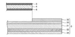
- FIG. It is sectional drawing which shows the positional relationship between the flexible wiring board and a plate in the optical module which concerns on Embodiment 1.
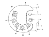
- FIG. It is a top view which shows the positional relationship between the flexible wiring board and a plate in the optical module which concerns on Embodiment 1.
- Embodiment 1 The optical module according to the first embodiment will be described with reference to FIGS. 1 to 4. In each figure, the same reference numerals indicate the same or corresponding parts.
- the optical modules covered by the present disclosure include an optical transmission module equipped with a semiconductor laser for optical communication, which is a light emitting element, an optical receiving module equipped with a photodiode for optical communication, which is a light receiving element, and an optical module for optical communication. It is a CAN package type optical module of an optical transmission / reception module equipped with a semiconductor laser and a photodiode for optical communication.
- the optical transmission module will be described as an example, but the relationship between the stem, the flexible printed circuits (FPC), the signal lead pin, the ground pin, and the plate is the optical receiving module and the optical. The same applies to the transmit / receive module.
- the optical module includes an optical module main body 1, a flexible wiring board 3, and a plate 4.
- the optical module main body 1 includes a stem 10, a lens cap 11, a lens 12, a signal lead pin 13, a ground pin 14, a thermoelectric cooler 15, a pedestal 16, a submount 17, and a semiconductor light emitting element which is a semiconductor laser. It includes 18, a termination resistor 19, and a dielectric substrate 20.
- the stem 10 is made of a disk-shaped metal, has an inner plane 10a and an outer plane 10b, and has a through hole 10c formed between the inner plane 10a and the outer plane 10b.
- the stem 10 functions as a heat sink for the semiconductor light emitting element 18, and the inner plane 10a serves as a component mounting region.
- the stem 10 is not limited to a disk shape, but may be a columnar shape or a square columnar shape, and may be a flat plate shape having an inner plane 10a and an outer plane 10b parallel to the inner plane 10a.
- the lens cap 11 is formed of a cylindrical metal having a bottomed portion and a side wall portion with one end open.
- a spherical glass lens 12 is mounted on the bottom of the lens cap 11, that is, an opening for mounting the lens to be mounted is formed.
- the lens 12 is mounted in the lens mounting opening of the bottom portion so that airtightness is maintained inside and outside the lens cap 11.
- the end face of the side wall portion of the lens cap 11, that is, the open end face at one end, is in contact with the peripheral end portion of the inner plane 10a of the stem 10 and is fixed by solder or the like.
- the open end face of the lens cap 11 is fixed to the inner plane 10a of the stem 10 so that the airtightness is maintained inside and outside the lens cap 11 even on the open end face. This fixing and mounting is performed at the end of the manufacturing process.
- the stem 10 and the lens cap 11 form a CAN type package.
- the signal lead pin 13 penetrates the through hole 10c of the stem 10 and is fixed to the stem 10 by an insulating glass 21 that is filled and solidified between the signal lead pin 13 and the through hole 10c.
- the insulating glass 21 electrically insulates the signal lead pin 13 and the stem 10 and seals the through hole 10c of the stem 10 to maintain the airtightness in the CAN type package.
- the signal lead pin 13 includes an inner lead portion 13a protruding from the inner plane 10a of the stem 10 and an outer lead portion 13b protruding from the outer plane 10b of the stem 10.
- the semiconductor light emitting device 18 is shown in the figure, there are also a light receiving element which is a photodiode that receives the back light of the semiconductor light emitting element 18 and monitors the output light, and a temperature adjusting device that adjusts the temperature of the semiconductor light emitting element 18. It is implemented in a CAN type package. Further, although not shown, a power supply pin for the semiconductor laser 18 and the light receiving element is also present, and is electrically isolated and fixed to the stem 10 like the signal lead pin 13.
- the ground pin 14 includes a pin portion 14a and a joint portion 14b at one end of the pin portion 14a, which has a diameter larger than the diameter of the pin portion 14a and is joined to the outer flat surface 10b of the stem 10.
- the diameter of the pin portion 14a is the same as the diameter of the signal lead pin 13.
- the ground pin 14 has a step between the pin portion 14a and the joint portion 14b, and the joint portion 14b is a step portion with respect to the pin portion 14a.
- the joint surface of the joint portion 14b of the ground pin 14 and the outer plane 10b of the stem 10 are joined by welding.
- the thermoelectric cooler 15 is mounted on the inner plane 10a of the stem 10 and cools the semiconductor light emitting element 18. The heat that cools the semiconductor light emitting device 18 is dissipated from the stem 10 to the outside.
- the thermoelectric cooler 15 is, for example, a Pelche element as a cooling element.
- the thermoelectric cooler 15 is not always necessary.
- a flat plate-shaped pedestal 16 is vertically erected and fixed on the thermoelectric cooler 15. When the thermoelectric cooler 15 is not required, the pedestal 16 is vertically upright and fixed to the inner plane 10a of the stem 10.
- the submount 17 is mounted on one plane of the pedestal 16, that is, mounted.
- the submount 17 is a ceramic substrate using aluminum nitride as a material having a coefficient of linear thermal expansion close to that of the semiconductor light emitting device 18.
- a semiconductor light emitting element 18 is mounted on one plane of the submount 17.
- the semiconductor light emitting device 18 is mounted on one flat surface of the submount 17 by die bonding with solder or a conductive adhesive or the like to a first electrode connection region provided by vapor deposition or the like on one flat surface of the submount 17. It is fixed. As a result, one electrode of the semiconductor light emitting device 18, that is, one signal terminal is electrically connected to the first electrode connection region. Further, the other electrode of the semiconductor light emitting device 18, that is, the other signal terminal is electrically connected to a second electrode connection region provided on one plane of the submount 17 by vapor deposition or the like by a gold wire 22a.
- a terminating resistor 19 is provided on one plane of the submount 17 by vapor deposition or the like.
- the terminating resistor 19 is a resistor for impedance matching with the IC that drives the semiconductor light emitting element 18, and is connected to the other signal terminal of the semiconductor light emitting element 18 by a gold wire 22b.
- the dielectric substrate 20 is mounted in a CAN type package, that is, it is arranged on the inner plane 10a of the stem 10, and a high frequency line connecting between the semiconductor light emitting device 18 and the signal lead pin 13 for the semiconductor light emitting device 18 is vapor-deposited. It is formed by such as.
- the dielectric substrate 20 serves as a bridging substrate between the semiconductor light emitting device 18 and the signal lead pin 13.
- the dielectric substrate 20 has a first electrode connection region to which one signal terminal of the semiconductor light emitting device 18 is connected, a first signal line region connected via a gold wire 22c, and a semiconductor light emitting device 18. It has a second electrode connection region to which the other signal terminal is connected and a second signal line region connected via a gold wire 22d, and each of the first signal line region and the second signal line region is gold. It is connected to different signal lead pins 13 via a wire (not shown).
- the first signal line region and the second signal line region are separate high-frequency lines.
- the semiconductor light emitting device 18 receives a modulation signal from the signal lead pin 13 and emits a laser beam corresponding to the modulation signal.
- the laser light emitted from the semiconductor light emitting device 18 is condensed or converted into parallel light through the lens 12 and irradiated to the outside.
- the dielectric substrate 20 is not always necessary. When the dielectric substrate 20 is not required, the first electrode connection region to which one signal terminal of the semiconductor light emitting device 18 is connected and the second electrode to which the other signal terminal of the semiconductor light emitting element 18 is connected. Each of the connection areas is directly connected to different signal lead pins 13 via a gold wire.
- the flexible wiring board 3 includes a flexible insulating substrate 31 such as polyimide, a wiring pattern 32 formed by vapor deposition or the like on the front surface of the insulating substrate 31, and a ground pattern 33 formed by vapor deposition or the like on the back surface of the insulating substrate 31. It has a power supply wiring layer (not shown) formed on the surface of the insulating substrate 31 by vapor deposition or the like, a front surface protective film 34, and a back surface protective film 35.
- a power supply wiring layer not shown
- the wiring pattern 32 has a plurality of signal wiring layers for transmitting high frequency signals.
- the surface of the wiring pattern 32 is covered and protected by the surface protective film 34.
- the first through hole 36 is formed at a position facing the signal lead pin 13 in the wiring pattern 32. As shown in FIG. 4, in the first through hole 36, three first through holes 36a to 36c are arranged along the circumference in the first embodiment.
- the semiconductor light emitting element 18, the light receiving element, and the temperature adjusting device are mounted in the CAN type package, and the semiconductor light emitting element 18, the light receiving element, and the signal lead pin 13 for the temperature adjusting device are provided, and the signal lead pin 13 is provided.
- An example in which the first through hole 36 corresponding to each is formed is shown. The subscripts of the symbols in the first through holes 36a to 36c may be omitted for the sake of brevity.
- the through hole has a conductive portion on the inner wall of the hole formed in the substrate, a front surface land on the front surface of the substrate, and a back surface land on the back surface, and the front surface land and the back surface land are electrically connected by the conductive portion. It is to conduct electricity.
- the outer lead portion 13b of the signal lead pin 13 penetrates the first through hole 36 in contact with the conductive portion, and the tip end portion of the outer lead portion 13b of the signal lead pin 13 is electrically connected to the wiring pattern 32.
- the tip of the outer lead portion 13b is fixed to the surface land of the first through hole 36 by solder 39, so that the signal lead pin 13 is electrically connected to the wiring pattern 32 via the first through hole 36. Ru.
- the ground pattern 33 is formed on substantially the entire back surface of the insulating substrate 31.
- the ground pattern 33 has an exposed surface at a position facing the outer plane of the stem 10, and the surface excluding the exposed surface is covered and protected by the back surface protective film 35.
- a second through hole 37 is formed at a position facing the ground pin 14 on the exposed surface of the ground pattern 33.
- the pin portion 14a of the gland pin 14 penetrates the second through hole 37 in contact with the conductive portion, and the tip end portion of the pin portion 14a of the gland pin 14 is fixed to the surface land of the second through hole 37 by the solder 40. ..
- the ground pin 14 is electrically connected to the ground pattern 33 via the front surface land-conducting portion-back surface land of the second through hole 37.
- a third through hole 38 is formed at a position where the power supply pin faces.
- the outer lead portion of the power supply pin penetrates the third through hole 38 in contact with the conductive portion, and the tip end portion of the outer lead portion of the power supply pin is electrically connected to the power supply pattern.
- the tip of the outer lead portion of the power supply pin is soldered to the surface land of the third through hole 38, so that the power supply pin is electrically connected to the power supply pattern via the third through hole 38.
- the plate 4 is a flat metal having a flat front surface and a back surface, the back surface is joined to the outer flat surface 10b of the stem 10, and the front surface is joined to the exposed surface of the ground pattern 33 of the flexible wiring board 3.
- the planar shape of the plate 4 is a shape in which the outer shape follows the outer shape of the outer plane 10b of the stem 10 and excludes the surface through which the signal lead pin 13 and the ground pin 14 are separated from each other.
- the plate 4 is a disk-shaped metal obtained by continuously hollowing out a portion through which a signal lead pin 13, a ground pin 14, and a power supply pin penetrate.
- the plate 4 may be a disk-shaped metal having a hole in a portion through which the signal lead pin 13, the ground pin 14, and the power supply pin penetrate.
- FIG. 4 shows a first through hole 36, a second through hole 37, and a third through hole 38.
- the back surface of the plate 4 and the outer flat surface 10b of the stem 10 are joined by the conductive tape 5.
- the conductive tape 5 fixes the plate 4 to the stem 10, and the plate 4 and the stem 10 are electrically connected.
- the back surface of the plate 4 and the outer flat surface 10b of the stem 10 may be joined and fixed by another conductive material.
- the bonding between the surface of the plate 4 and the exposed surface of the ground pattern 33 of the flexible wiring board 3 is performed by the conductive adhesive 6.
- the plate 4 is fixed to the flexible wiring board 3 by the conductive adhesive 6, and the plate 4 and the ground pattern 33 are electrically connected to each other.
- the conductive adhesive 6 the surface of the plate 4 and the exposed surface of the ground pattern 33 of the flexible wiring board 3 may be joined and fixed by another conductive material.
- the stem 10 is electrically connected to the ground pattern 33 of the flexible wiring board 3 via the conductive tape 5-plate 4-conductive adhesive 6, and the stem 10 and the ground pattern 33 have a common ground.
- the tip portion of the pin portion 14a is electrically connected to the ground pattern 33 of the flexible wiring board 30, and one end of the pin portion 14a has a diameter larger than the diameter of the pin portion 14a.
- a metal plate 4 is interposed between the stem 10 and the exposed surface of the ground pattern 33. Since the connection is made electrically and mechanically, the diameter of the through hole 37 for the ground pin 14 can be made a size that matches the diameter of the pin portion 14a, and the degree of freedom in wiring design in the flexible wiring board 30 is not impaired. .. That is, it is not necessary to increase the diameter of the through hole 37 for the ground pin 14 in accordance with the joint portion 14b having a diameter larger than the diameter of the pin portion 14a, and the degree of freedom in wiring design is not hindered.
- the tip of the outer lead portion 13b of the signal lead pin 13 is fixed to the surface land of the first through hole 36 by solder 39, and the tip of the pin portion 14a of the ground pin 14 is attached to the surface land of the second through hole 37.
- the solder 40 By being fixed by the solder 40, the flexible wiring board 30, the plate 4, and the stem 10 are firmly adhered to each other.
- the electrical and mechanical connection between the stem 10 and the ground pattern 33 can be reliably and firmly maintained.
- the plate 4 is bonded to the exposed surface of the ground pattern 33 of the flexible wiring board 30 with a conductive adhesive 6, the conductive tape 5 is attached to the surface of the plate 4 bonded to the flexible wiring board 30, and the stem 10 is conductive. Since it is bonded to the plate 4 by the tape 5, the optical module can be assembled without modifying the optical module main body 1 and the flexible wiring board 3.
- the stem 10 is fixed to the flexible wiring board 3 by the conductive tape 5 and the conductive adhesive 6, the tip of the outer lead portion 13b of the signal lead pin 13 and the surface land of the first through hole 36 Soldering 39 and soldering 40 between the tip of the pin portion 14a of the gland pin 14 and the surface land of the second through hole 37 are easy.
- ground pattern 33 of the stem 10 and the flexible wiring board 30 is electrically connected to the ground potential by the metal plate 4, the ground potential near the signal lead pin 13 is strengthened, and the stem 10 and the flexible wiring board are strengthened. The parallel plate resonance due to the ground pattern 33 of 30 can be suppressed.
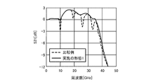
- the passage characteristic S21 with respect to the frequency in the optical module according to the first embodiment was calculated.
- the pass characteristic S21 with respect to the frequency in the optical module using the plate 4 made of an insulator made of polyimide instead of metal was also calculated.
- the calculation result is shown in FIG. In FIG. 5, the horizontal axis represents the frequency, the vertical axis represents the passage characteristic S21, the solid line is the calculation result in the optical module according to the first embodiment, and the dotted line is the calculation result in the comparative example.
- the pass characteristic S21 with respect to the frequency in the optical module according to the first embodiment is better than the pass characteristic S21 with respect to the frequency in the comparative example.
- the optical module according to the first embodiment is electrically and mechanically connected by interposing a metal plate 4 between the stem 10 and the exposed surface of the ground pattern 33 of the flexible wiring board 30. Resonance and multiple reflections between the stem 10 and the ground pattern 33 can be suppressed, and good frequency characteristics are obtained.
- the optical module according to the present disclosure can be used as an optical transmission module for optical communication, as an optical reception module for optical communication equipped with a light receiving element, and a light emitting element and a light receiving element. It can be used as an optical transmission / reception module equipped with both elements.
- Optical module body 10 stem, 10a inner plane, 10b outer plane, 10c through hole, 13 signal lead pin, 13a inner lead part, 13b outer lead part, 14 ground pin, 14a pin part, 14b junction, 18 semiconductor light emission Element, 20 dielectric substrate, 3 flexible wiring board, 31 insulation substrate, 32 wiring pattern, 33 ground pattern, 36a to 36c first through hole, 37 second through hole, 4 plate, 5 conductive tape, 6 conductive Sex adhesive.
Landscapes
- Engineering & Computer Science (AREA)
- Microelectronics & Electronic Packaging (AREA)
- Physics & Mathematics (AREA)
- Electromagnetism (AREA)
- Semiconductor Lasers (AREA)
- Light Receiving Elements (AREA)
Abstract
Description
特許文献1には、ステムとフレキシブル配線基板との結合部分におけるエネルギー損失を抑制するために、ステムのグランド面とフレキシブル配線基板のグランド面とを接触させたTO-CAN(Transistor Outlined CAN)型TOSA(Transmitter Optical Sub-Assembly)モジュールが示されている。
この種の光モジュールは、グランドピンは細く、細いままステムの外表面にグランドピンを溶接したのでは、ステムの外表面とグランドピンとの固定が不十分になりやすいため、ステムの外表面との溶接部分、つまり、グランドピンの根元部分に直径が他の部分の直径より大きくした溶接部を設けるのが一般的である。
スルーホールの穴径を大きくとると、フレキシブル配線基板に形成される配線に使用できる面積が減り、配線設計の自由度が減ってしまうという課題がある。
実施の形態1に係る光モジュールを図1から図4を用いて説明する。
なお、各図中、同一符号は同一又は相当部分を示す。
本開示が対象とする光モジュールは、発光素子である光通信用の半導体レーザが搭載された光送信モジュール、受光素子である光通信用のフォトダイオードが搭載された光受信モジュール、光通信用の半導体レーザ及び光通信用のフォトダイオードが搭載された光送受信モジュールのCANパッケージ型光モジュールである。
実施の形態1では、光送信モジュールを例にとり説明するが、ステムと、フレキシブル配線基板(FPC:Flexible printed circuits)と、信号用リードピンと、グランドピンと、プレートとの関係は、光受信モジュール及び光送受信モジュールにおいても同じである。
光モジュール本体1は、ステム10、レンズキャップ11と、レンズ12と、信号用リードピン13と、グランドピン14と、熱電クーラー15と、台座16と、サブマウント17と、半導体レーザである半導体発光素子18と、終端抵抗19と、誘電体基板20を備える。
ステム10は半導体発光素子18のヒートシンクとして機能するとともに、内平面10aが部品実装用の領域となる。
なお、ステム10は円板状に限られるものでなく、円柱状もしくは四角柱状でも良く、内平面10aと内平面10aと平行な外平面10bを有する平板状であれば良い。
ステム10とレンズキャップ11とによりCAN型パッケージを構成する。
信号用リードピン13は、ステム10の内平面10aから突出したインナーリード部13aと、ステム10の外平面10bから突出したアウターリード部13bを具備する。
また、図示していないが、半導体レーザ18及び受光素子などに対する電源ピンも存在し、信号用リードピン13と同様にステム10と電気的に絶縁されて固定される。
グランドピン14は、ピン部14aと接合部14bとの間に段差を有し、接合部14bは、ピン部14aに対して段差部となる。
グランドピン14における接合部14bの接合面とステム10の外平面10bとは溶接により接合される。
熱電クーラー15の上に平板状の台座16が垂直に直立されて固定される。熱電クーラー15を必要としない場合は、台座16は、ステム10の内平面10aに垂直に直立されて固定される。
サブマウント17の一平面には半導体発光素子18が搭載される。
これにより、半導体発光素子18の一方の電極、つまり、一方の信号端子は第1の電極接続領域に電気的に接続される。
また、半導体発光素子18の他方の電極、つまり、他方の信号端子は、サブマウント17の一平面に蒸着等により設けられた第2の電極接続領域に金線22aによって電気的に接続される。
終端抵抗19は半導体発光素子18を駆動するICとのインピーダンス整合をとるための抵抗であり、金線22bによって半導体発光素子18の他方の信号端子に接続される。
誘電体基板20は半導体発光素子18と信号用リードピン13との橋渡し基板としての役割を担う。
第1の信号線領域及び第2の信号線領域それぞれ、別の高周波線路である。
絶縁基板31は、配線パターン32における信号用リードピン13が対向する位置に第1のスルーホール36が形成される。第1のスルーホール36は、図4に示すように、実施の形態1では3つの第1のスルーホール36a~36cが円周に沿って配置されている。
なお、第1のスルーホール36a~36cにおける符号の添字は、説明の簡略のため、省略して説明する場合がある。
アウターリード部13bの先端部が第1のスルーホール36の表面ランドにはんだ39により固着されることにより、信号用リードピン13は第1のスルーホール36を介して配線パターン32に電気的に接続される。
絶縁基板31は、グランドパターン33の露出面におけるグランドピン14が対向する位置に第2のスルーホール37が形成される。
その結果、グランドピン14は、第2のスルーホール37の表面ランド-導通部-裏面ランドを介してグランドパターン33に電気的に接続される。
電源ピンのアウターリード部が第3のスルーホール38を導通部に接して貫通し、電源ピンのアウターリード部の先端部が電源パターンに電気的に接続される。
電源ピンのアウターリード部の先端部が第3のスルーホール38の表面ランドにはんだにより固着されることにより、電源ピンは第3のスルーホール38を介して電源パターンに電気的に接続される。
すなわち、プレート4は、円板状の金属を、信号用リードピン13、グランドピン14及び電源ピンが貫通する部分を連続的にくり抜いたものである。なお、プレート4は、円板状の金属を、信号用リードピン13、グランドピン14及び電源ピンが貫通する部分に穴をあけたものでもよい。
図4に、第1のスルーホール36、第2のスルーホール37、第3のスルーホール38を示している。
なお、導電性テープ5の代わりに他の導電性材料によりプレート4の裏面とステム10の外平面10bとを接合し、固定してもよい。
なお、導電性接着剤6の代わりに他の導電性材料によりプレート4の表面とフレキシブル配線基板3のグランドパターン33の露出面とを接合し、固定してもよい。
ステム10は、導電性テープ5-プレート4-導電性接着剤6を介してフレキシブル配線基板3のグランドパターン33と電気的に接続され、ステム10とグランドパターン33はグランドが共通化される。
すなわち、ピン部14aの径より径が大きい接合部14bに合わせて、グランドピン14のためのスルーホール37の径を大きくする必要がなく、配線設計の自由度が妨げられない。
その結果、導電性テープ5及び導電性接着剤6と合わせて、ステム10とグランドパターン33との電気的及び機械的な接続を確実にかつ強固に維持できる。
比較のために、プレート4を金属製ではなく、ポリイミドからなる絶縁体のプレートを用いた光モジュールにおける周波数に対する通過特性S21も演算した。
図5において、横軸が周波数、縦軸が通過特性S21を示し、実線が実施の形態1に係る光モジュールにおける演算結果、点線が比較例における演算結果である。
図5から理解できるように、実施の形態1に係る光モジュールにおける周波数に対する通過特性S21は、比較例における周波数に対する通過特性S21より良好であることが分かる。
Claims (5)
- 内平面と外平面を有し、前記内平面と前記外平面との間を貫通した貫通孔が形成された金属製のステムと、
前記ステムの貫通孔を貫通して前記ステムと電気的に絶縁されて固定され、前記ステムの内平面から突出したインナーリード部と、前記ステムの外平面から突出したアウターリード部を具備する信号用リードピンと、
ピン部と、このピン部の一端に当該ピン部の径より径が大きく、前記ステムの外平面に接合される接合部を具備するグランドピンと、
表面に配線パターンを具備し、裏面に前記ステムの外平面に対向する位置に露出面を有するグランドパターンを具備し、前記配線パターンにおける前記信号用リードピンが対向する位置に第1のスルーホールが形成され、前記信号用リードピンのアウターリード部が前記第1のスルーホールを貫通し、前記信号用リードピンのアウターリード部の先端部が前記配線パターンに電気的に接続され、前記グランドパターンの露出面における前記グランドピンが対向する位置に第2のスルーホールが形成され、前記グランドピンのピン部が前記第2のスルーホールを貫通し、前記グランドピンのピン部の先端部が表面において前記第2のスルーホールと電気的に接続されたフレキシブル配線基板と、
裏面が前記ステムの外平面に接合され、表面が前記グランドパターンの露出面に接合された金属製のプレートと、
を備えた光モジュール。 - 前記グランドパターンの露出面と前記プレートの表面との接合は導電性接着剤で行われ、前記ステムの外平面と前記プレートの裏面との接合は導電性テープで行われた請求項1に記載の光モジュール。
- 前記プレートの平面形状は、外形が前記ステムの外平面の外形に沿い、前記信号用リードピン及び前記グランドピンが離隔して貫通する面を除いた形状である請求項1又は請求項2に記載の光モジュール。
- 前記ステムと、前記ステムの内平面における周端部に接して固着されるレンズキャップとにより構成されるCAN型パッケージ内に、半導体発光素子、受光素子、及び温度調整機器が実装され、
前記信号用リードピンは、前記半導体発光素子に対する信号用リードピンとして構成される請求項1から請求項3のいずれか1項に記載の光モジュール。 - 前記半導体発光素子と前記半導体発光素子に対する信号用リードピンとの間を接続する高周波線路を有する誘電体基板が、前記CAN型パッケージ内に実装される請求項4に記載の光モジュール。
Priority Applications (4)
| Application Number | Priority Date | Filing Date | Title |
|---|---|---|---|
| PCT/JP2020/043684 WO2022113174A1 (ja) | 2020-11-24 | 2020-11-24 | 光モジュール |
| JP2022562924A JP7204065B2 (ja) | 2020-11-24 | 2020-11-24 | 光モジュール |
| CN202080107228.4A CN116648835B (zh) | 2020-11-24 | 2020-11-24 | 光模块 |
| US18/179,606 US12256497B2 (en) | 2020-11-24 | 2023-03-07 | Optical module |
Applications Claiming Priority (1)
| Application Number | Priority Date | Filing Date | Title |
|---|---|---|---|
| PCT/JP2020/043684 WO2022113174A1 (ja) | 2020-11-24 | 2020-11-24 | 光モジュール |
Related Child Applications (1)
| Application Number | Title | Priority Date | Filing Date |
|---|---|---|---|
| US18/179,606 Continuation US12256497B2 (en) | 2020-11-24 | 2023-03-07 | Optical module |
Publications (1)
| Publication Number | Publication Date |
|---|---|
| WO2022113174A1 true WO2022113174A1 (ja) | 2022-06-02 |
Family
ID=81754112
Family Applications (1)
| Application Number | Title | Priority Date | Filing Date |
|---|---|---|---|
| PCT/JP2020/043684 Ceased WO2022113174A1 (ja) | 2020-11-24 | 2020-11-24 | 光モジュール |
Country Status (4)
| Country | Link |
|---|---|
| US (1) | US12256497B2 (ja) |
| JP (1) | JP7204065B2 (ja) |
| CN (1) | CN116648835B (ja) |
| WO (1) | WO2022113174A1 (ja) |
Citations (3)
| Publication number | Priority date | Publication date | Assignee | Title |
|---|---|---|---|---|
| JP2005228766A (ja) * | 2004-02-10 | 2005-08-25 | Opnext Japan Inc | 光送信機 |
| JP2012256692A (ja) * | 2011-06-08 | 2012-12-27 | Mitsubishi Electric Corp | 光モジュール |
| CN110798967A (zh) * | 2019-11-30 | 2020-02-14 | 光为科技(广州)有限公司 | 软板结构、to光模块及光传输装置 |
Family Cites Families (14)
| Publication number | Priority date | Publication date | Assignee | Title |
|---|---|---|---|---|
| JPH11150218A (ja) * | 1997-11-19 | 1999-06-02 | Sumitomo Electric Ind Ltd | 半導体ステムとその製造方法及び光半導体モジュール |
| JP4756840B2 (ja) * | 2004-09-13 | 2011-08-24 | 三菱電機株式会社 | キャンパッケージ型光半導体装置および光モジュール |
| JP2010098112A (ja) * | 2008-10-16 | 2010-04-30 | Shinko Electric Ind Co Ltd | 光半導体用ステムおよび光半導体ステムの電解金めっき方法と、光半導体装置 |
| JP2011108940A (ja) | 2009-11-19 | 2011-06-02 | Nippon Telegr & Teleph Corp <Ntt> | To−can型tosaモジュール用実装構成およびto−can型tosaモジュール |
| JP5616178B2 (ja) * | 2010-09-16 | 2014-10-29 | 京セラ株式会社 | 電子部品搭載用パッケージおよび通信用モジュール |
| JP2013004833A (ja) * | 2011-06-20 | 2013-01-07 | Nippon Telegr & Teleph Corp <Ntt> | 高周波モジュール及びその高周波線路の接続方法 |
| JP6430160B2 (ja) * | 2014-07-07 | 2018-11-28 | 日本オクラロ株式会社 | 光モジュール及び光モジュールの製造方法 |
| JP6445268B2 (ja) * | 2014-07-11 | 2018-12-26 | 日本オクラロ株式会社 | 光モジュール、光送受信モジュール、及びフレキシブル基板 |
| JP6654364B2 (ja) * | 2015-06-12 | 2020-02-26 | 日本ルメンタム株式会社 | 光モジュール |
| JP6600546B2 (ja) * | 2015-12-11 | 2019-10-30 | 日本ルメンタム株式会社 | 光モジュール |
| JP2018073943A (ja) * | 2016-10-27 | 2018-05-10 | 住友電気工業株式会社 | 半導体発光装置、ステム部品 |
| JP6777227B2 (ja) * | 2017-05-17 | 2020-10-28 | 三菱電機株式会社 | 光モジュールおよびその製造方法 |
| EP3667378B1 (en) * | 2017-07-11 | 2026-04-08 | Yokowo Co., Ltd. | Optical module |
| JP7240160B2 (ja) * | 2018-12-11 | 2023-03-15 | 新光電気工業株式会社 | ステム |
-
2020
- 2020-11-24 JP JP2022562924A patent/JP7204065B2/ja active Active
- 2020-11-24 CN CN202080107228.4A patent/CN116648835B/zh active Active
- 2020-11-24 WO PCT/JP2020/043684 patent/WO2022113174A1/ja not_active Ceased
-
2023
- 2023-03-07 US US18/179,606 patent/US12256497B2/en active Active
Patent Citations (3)
| Publication number | Priority date | Publication date | Assignee | Title |
|---|---|---|---|---|
| JP2005228766A (ja) * | 2004-02-10 | 2005-08-25 | Opnext Japan Inc | 光送信機 |
| JP2012256692A (ja) * | 2011-06-08 | 2012-12-27 | Mitsubishi Electric Corp | 光モジュール |
| CN110798967A (zh) * | 2019-11-30 | 2020-02-14 | 光为科技(广州)有限公司 | 软板结构、to光模块及光传输装置 |
Also Published As
| Publication number | Publication date |
|---|---|
| JPWO2022113174A1 (ja) | 2022-06-02 |
| CN116648835B (zh) | 2025-03-21 |
| US20230209718A1 (en) | 2023-06-29 |
| CN116648835A (zh) | 2023-08-25 |
| JP7204065B2 (ja) | 2023-01-13 |
| US12256497B2 (en) | 2025-03-18 |
Similar Documents
| Publication | Publication Date | Title |
|---|---|---|
| KR101430634B1 (ko) | 광 모듈 | |
| JP6614811B2 (ja) | 半導体装置用ステム及び半導体装置 | |
| JP4015440B2 (ja) | 光通信モジュール | |
| WO2018219318A1 (zh) | 同轴封装的激光器和光模块 | |
| CN113875103A (zh) | 光模块 | |
| JP2003229629A (ja) | 光モジュール | |
| JP6984801B1 (ja) | 半導体レーザ光源装置 | |
| JP2008226988A (ja) | 光電変換モジュール | |
| KR102777084B1 (ko) | 반도체 장치용 헤더 및 반도체 장치 | |
| WO2022123659A1 (ja) | レーザ光源装置 | |
| JP4587218B2 (ja) | パッケージ型半導体装置 | |
| US7255494B2 (en) | Low-profile package for housing an optoelectronic assembly | |
| JP2008103774A (ja) | 高周波光伝送モジュールおよび光伝送器 | |
| JP7544304B1 (ja) | 光モジュールおよび光トランシーバ | |
| US7192201B2 (en) | Optical transmitting module having a de-coupling inductor therein | |
| JP4105647B2 (ja) | 半導体レーザモジュール及び光伝送器 | |
| JP2004335584A (ja) | 半導体パッケージ | |
| US12256497B2 (en) | Optical module | |
| TWI863260B (zh) | 半導體雷射光源裝置 | |
| JP7542466B2 (ja) | 光モジュール | |
| JP7246590B1 (ja) | 半導体レーザ光源装置 | |
| JP2005159060A (ja) | 同軸型半導体レーザモジュール | |
| JP2021141302A (ja) | 光モジュール | |
| JP2013120773A (ja) | 光送信モジュール | |
| JP2006324391A (ja) | 電子部品収納用パッケージおよび電子装置 |
Legal Events
| Date | Code | Title | Description |
|---|---|---|---|
| 121 | Ep: the epo has been informed by wipo that ep was designated in this application |
Ref document number: 20963439 Country of ref document: EP Kind code of ref document: A1 |
|
| ENP | Entry into the national phase |
Ref document number: 2022562924 Country of ref document: JP Kind code of ref document: A |
|
| WWE | Wipo information: entry into national phase |
Ref document number: 202080107228.4 Country of ref document: CN |
|
| NENP | Non-entry into the national phase |
Ref country code: DE |
|
| 122 | Ep: pct application non-entry in european phase |
Ref document number: 20963439 Country of ref document: EP Kind code of ref document: A1 |
|
| WWG | Wipo information: grant in national office |
Ref document number: 202080107228.4 Country of ref document: CN |