WO2022097328A1 - 共振装置及び共振装置製造方法 - Google Patents
共振装置及び共振装置製造方法 Download PDFInfo
- Publication number
- WO2022097328A1 WO2022097328A1 PCT/JP2021/025075 JP2021025075W WO2022097328A1 WO 2022097328 A1 WO2022097328 A1 WO 2022097328A1 JP 2021025075 W JP2021025075 W JP 2021025075W WO 2022097328 A1 WO2022097328 A1 WO 2022097328A1
- Authority
- WO
- WIPO (PCT)
- Prior art keywords
- layer
- resonator
- substrate
- metal
- metal layer
- Prior art date
- Legal status (The legal status is an assumption and is not a legal conclusion. Google has not performed a legal analysis and makes no representation as to the accuracy of the status listed.)
- Ceased
Links
Images






Classifications
-
- H—ELECTRICITY
- H03—ELECTRONIC CIRCUITRY
- H03H—IMPEDANCE NETWORKS, e.g. RESONANT CIRCUITS; RESONATORS
- H03H9/00—Networks comprising electromechanical or electro-acoustic elements; Electromechanical resonators
- H03H9/02—Details
- H03H9/05—Holders or supports
- H03H9/10—Mounting in enclosures
- H03H9/1057—Mounting in enclosures for microelectro-mechanical devices
-
- H—ELECTRICITY
- H03—ELECTRONIC CIRCUITRY
- H03H—IMPEDANCE NETWORKS, e.g. RESONANT CIRCUITS; RESONATORS
- H03H9/00—Networks comprising electromechanical or electro-acoustic elements; Electromechanical resonators
- H03H9/15—Constructional features of resonators consisting of piezoelectric or electrostrictive material
- H03H9/17—Constructional features of resonators consisting of piezoelectric or electrostrictive material having a single resonator
- H03H9/171—Constructional features of resonators consisting of piezoelectric or electrostrictive material having a single resonator implemented with thin-film techniques, i.e. of the film bulk acoustic resonator [FBAR] type
-
- B—PERFORMING OPERATIONS; TRANSPORTING
- B23—MACHINE TOOLS; METAL-WORKING NOT OTHERWISE PROVIDED FOR
- B23K—SOLDERING OR UNSOLDERING; WELDING; CLADDING OR PLATING BY SOLDERING OR WELDING; CUTTING BY APPLYING HEAT LOCALLY, e.g. FLAME CUTTING; WORKING BY LASER BEAM
- B23K20/00—Non-electric welding by applying impact or other pressure, with or without the application of heat, e.g. cladding or plating
- B23K20/002—Non-electric welding by applying impact or other pressure, with or without the application of heat, e.g. cladding or plating specially adapted for particular articles or work
- B23K20/004—Wire welding
-
- B—PERFORMING OPERATIONS; TRANSPORTING
- B23—MACHINE TOOLS; METAL-WORKING NOT OTHERWISE PROVIDED FOR
- B23K—SOLDERING OR UNSOLDERING; WELDING; CLADDING OR PLATING BY SOLDERING OR WELDING; CUTTING BY APPLYING HEAT LOCALLY, e.g. FLAME CUTTING; WORKING BY LASER BEAM
- B23K20/00—Non-electric welding by applying impact or other pressure, with or without the application of heat, e.g. cladding or plating
- B23K20/02—Non-electric welding by applying impact or other pressure, with or without the application of heat, e.g. cladding or plating by means of a press ; Diffusion bonding
-
- B—PERFORMING OPERATIONS; TRANSPORTING
- B23—MACHINE TOOLS; METAL-WORKING NOT OTHERWISE PROVIDED FOR
- B23K—SOLDERING OR UNSOLDERING; WELDING; CLADDING OR PLATING BY SOLDERING OR WELDING; CUTTING BY APPLYING HEAT LOCALLY, e.g. FLAME CUTTING; WORKING BY LASER BEAM
- B23K20/00—Non-electric welding by applying impact or other pressure, with or without the application of heat, e.g. cladding or plating
- B23K20/18—Zonal welding by interposing weld-preventing substances between zones not to be welded
-
- B—PERFORMING OPERATIONS; TRANSPORTING
- B81—MICROSTRUCTURAL TECHNOLOGY
- B81C—PROCESSES OR APPARATUS SPECIALLY ADAPTED FOR THE MANUFACTURE OR TREATMENT OF MICROSTRUCTURAL DEVICES OR SYSTEMS
- B81C3/00—Assembling of devices or systems from individually processed components
- B81C3/001—Bonding of two components
-
- H—ELECTRICITY
- H03—ELECTRONIC CIRCUITRY
- H03H—IMPEDANCE NETWORKS, e.g. RESONANT CIRCUITS; RESONATORS
- H03H3/00—Apparatus or processes specially adapted for the manufacture of impedance networks, resonating circuits, resonators
- H03H3/007—Apparatus or processes specially adapted for the manufacture of impedance networks, resonating circuits, resonators for the manufacture of electromechanical resonators or networks
- H03H3/0072—Apparatus or processes specially adapted for the manufacture of impedance networks, resonating circuits, resonators for the manufacture of electromechanical resonators or networks of microelectro-mechanical resonators or networks
-
- H—ELECTRICITY
- H03—ELECTRONIC CIRCUITRY
- H03H—IMPEDANCE NETWORKS, e.g. RESONANT CIRCUITS; RESONATORS
- H03H3/00—Apparatus or processes specially adapted for the manufacture of impedance networks, resonating circuits, resonators
- H03H3/007—Apparatus or processes specially adapted for the manufacture of impedance networks, resonating circuits, resonators for the manufacture of electromechanical resonators or networks
- H03H3/02—Apparatus or processes specially adapted for the manufacture of impedance networks, resonating circuits, resonators for the manufacture of electromechanical resonators or networks for the manufacture of piezoelectric or electrostrictive resonators or networks
-
- H—ELECTRICITY
- H03—ELECTRONIC CIRCUITRY
- H03H—IMPEDANCE NETWORKS, e.g. RESONANT CIRCUITS; RESONATORS
- H03H9/00—Networks comprising electromechanical or electro-acoustic elements; Electromechanical resonators
- H03H9/24—Constructional features of resonators of material which is not piezoelectric, electrostrictive, or magnetostrictive
- H03H9/2405—Constructional features of resonators of material which is not piezoelectric, electrostrictive, or magnetostrictive of microelectro-mechanical resonators
- H03H9/2468—Tuning fork resonators
- H03H9/2478—Single-Ended Tuning Fork resonators
- H03H9/2489—Single-Ended Tuning Fork resonators with more than two fork tines
-
- B—PERFORMING OPERATIONS; TRANSPORTING
- B81—MICROSTRUCTURAL TECHNOLOGY
- B81B—MICROSTRUCTURAL DEVICES OR SYSTEMS, e.g. MICROMECHANICAL DEVICES
- B81B2201/00—Specific applications of microelectromechanical systems
- B81B2201/02—Sensors
- B81B2201/0271—Resonators; ultrasonic resonators
-
- B—PERFORMING OPERATIONS; TRANSPORTING
- B81—MICROSTRUCTURAL TECHNOLOGY
- B81B—MICROSTRUCTURAL DEVICES OR SYSTEMS, e.g. MICROMECHANICAL DEVICES
- B81B2201/00—Specific applications of microelectromechanical systems
- B81B2201/03—Microengines and actuators
- B81B2201/032—Bimorph and unimorph actuators, e.g. piezo and thermo
-
- B—PERFORMING OPERATIONS; TRANSPORTING
- B81—MICROSTRUCTURAL TECHNOLOGY
- B81B—MICROSTRUCTURAL DEVICES OR SYSTEMS, e.g. MICROMECHANICAL DEVICES
- B81B2207/00—Microstructural systems or auxiliary parts thereof
- B81B2207/07—Interconnects
-
- B—PERFORMING OPERATIONS; TRANSPORTING
- B81—MICROSTRUCTURAL TECHNOLOGY
- B81C—PROCESSES OR APPARATUS SPECIALLY ADAPTED FOR THE MANUFACTURE OR TREATMENT OF MICROSTRUCTURAL DEVICES OR SYSTEMS
- B81C2203/00—Forming microstructural systems
- B81C2203/03—Bonding two components
- B81C2203/033—Thermal bonding
- B81C2203/035—Soldering
Definitions
- the present invention relates to a resonance device and a method for manufacturing a resonance device.
- a resonance device manufactured by using MEMS Micro Electro Mechanical Systems
- This device is formed by joining an upper substrate to, for example, a lower substrate having a resonator.
- Patent Document 1 includes a lower substrate having a resonator, an upper substrate provided facing the element, and a joint portion for joining the lower substrate and the upper substrate around the element.
- a MEMS device having a region containing a hypereutectic alloy and a region containing a eutectic alloy is disclosed as a junction.
- the hypereutectic alloy covers the eutectic alloy to prevent the metal from squeezing out from the joint surface of the eutectic joint.
- the characteristics of the MEMS device may be improved by connecting the joint portion to the ground (GND) to suppress the generation of parasitic capacitance (stray capacitance).
- the joint and the lower electrode of the resonator were connected by an aluminum (Al) wiring having good electrical connectivity.
- the metal constituting the joining portion for example, germanium (Ge)
- the metal constituting the joining portion diffuses into the aluminum wiring and flows into the lower electrode side of the resonator. Therefore, the ratio of the metals constituting the joint portion may change, the eutectic ratio (eutectic ratio) may change, or the eutectic reaction may become insufficient.
- joint defects such as a decrease in the joint strength of the joint portion occur.
- the present invention has been made in view of such circumstances, and one of the objects of the present invention is to provide a resonance device and a method for manufacturing a resonance device capable of suppressing joint defects in a joint portion.
- the resonance device includes a first substrate including a resonator, a second substrate, and a joint portion having conductivity and joining the first substrate and the second substrate.
- One substrate further includes a wiring layer that is electrically connected to the lower electrode of the resonator and a diffusion prevention layer that electrically connects the wiring layer and the joint portion.
- a method for manufacturing a resonator according to another aspect of the present invention includes a first metal layer, a resonator, a wiring layer electrically connected to a lower electrode of the resonator, and the wiring layer and the first metal layer.
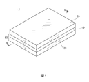
- FIG. 1 is a perspective view schematically showing the appearance of the resonance device according to the embodiment of the present invention.
- FIG. 2 is an exploded perspective view schematically showing the structure of the resonance apparatus shown in FIG.
- FIG. 3 is a plan view schematically showing the structure of the resonator shown in FIG.
- FIG. 4 is a cross-sectional view schematically showing the configuration of a cross section of the resonator shown in FIGS. 1 to 3 along the IV-IV line.
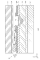
- FIG. 5 is an enlarged cross-sectional view of a main part schematically showing the configuration of the joint portion shown in FIG. 4 and its surroundings.
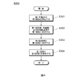
- FIG. 6 is a flowchart showing a method of manufacturing a resonance device according to an embodiment.
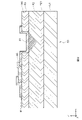
- FIG. 7 is a cross-sectional view for explaining the process shown in FIG.
- FIG. 8 is an enlarged cross-sectional view of a main part for explaining the first example of the process shown in FIG.
- FIG. 9 is an enlarged cross-sectional view of a main part for explaining a second example of the process shown in FIG.
- FIG. 10 is an enlarged cross-sectional view of a main part for explaining a third example of the process shown in FIG.
- FIG. 11 is an enlarged cross-sectional view of a main part for explaining a fourth example of the process shown in FIG.
- FIG. 12 is an enlarged cross-sectional view of a main part for explaining the process shown in FIG.
- FIG. 13 is an enlarged plan view of a main part for explaining the process shown in FIG.
- FIG. 14 is an enlarged cross-sectional view of a main part showing a third modification of the joint portion shown in FIG.
- FIG. 1 is a perspective view schematically showing the appearance of the resonance device 1 in one embodiment.
- FIG. 2 is an exploded perspective view schematically showing the structure of the resonance device 1 shown in FIG.
- the resonator 1 includes a lower lid 20, a resonator 10 (hereinafter, the lower lid 20 and the resonator 10 are collectively referred to as a “MEMS substrate 50”), and an upper lid 30. That is, the resonator 1 is configured by laminating the MEMS substrate 50, the joint portion 60, and the upper lid 30 in this order.
- the MEMS substrate 50 corresponds to an example of the "first substrate” of the present invention
- the upper lid 30 corresponds to an example of the "second substrate” of the present invention.
- the side of the resonance device 1 where the upper lid 30 is provided is referred to as the upper side (or the front side), and the side where the lower lid 20 is provided is referred to as the lower side (or the back side).
- the resonator 10 is a MEMS oscillator manufactured using MEMS technology.
- the resonator 10 and the upper lid 30 are joined via a joint portion 60, which will be described later.
- the resonator 10 and the lower lid 20 are each formed of a silicon (Si) substrate (hereinafter referred to as “Si substrate”), and the Si substrates are bonded to each other.
- the MEMS substrate 50 (resonator 10 and lower lid 20) may be formed by using an SOI substrate.
- the upper lid 30 extends in a flat plate shape along the XY plane, and for example, a flat rectangular parallelepiped concave portion 31 is formed on the back surface thereof.
- the recess 31 is surrounded by the side wall 33 and forms a part of the vibration space, which is the space where the resonator 10 vibrates.
- a getter layer 34 which will be described later, is formed on the surface of the concave portion 31 of the upper lid 30 on the resonator 10 side.
- the upper lid 30 does not have a recess 31, and may have a flat plate shape.
- the lower lid 20 includes a rectangular flat plate-shaped bottom plate 22 provided along the XY plane, and a side wall 23 extending in the Z-axis direction from the peripheral edge of the bottom plate 22, that is, in the stacking direction of the lower lid 20 and the resonator 10.
- the lower lid 20 is formed with a recess 21 formed by the surface of the bottom plate 22 and the inner surface of the side wall 23 on the surface facing the resonator 10.
- the recess 21 forms a part of the vibration space of the resonator 10.
- the lower lid 20 does not have the recess 21 and may have a flat plate shape. Further, a getter layer may be formed on the surface of the lower lid 20 on the resonator 10 side of the recess 21.
- FIG. 3 is a plan view schematically showing the structure of the resonator 10 shown in FIG.
- the resonator 10 is a MEMS oscillator manufactured by using the MEMS technique, and vibrates out of the plane in the XY plane in the Cartesian coordinate system of FIG.
- the resonator 10 is not limited to the resonator using the out-of-plane bending vibration mode.
- the resonator of the resonator 1 may use, for example, a spread vibration mode, a thickness longitudinal vibration mode, a lamb wave vibration mode, an in-plane bending vibration mode, and a surface wave vibration mode.
- These oscillators are applied to, for example, timing devices, RF filters, duplexers, ultrasonic transducers, gyro sensors, acceleration sensors and the like.
- a piezoelectric mirror having an actuator function
- a piezoelectric gyro having a pressure sensor function
- an ultrasonic vibration sensor or the like.
- it may be applied to an electrostatic MEMS element, an electromagnetically driven MEMS element, and a piezo resistance MEMS element.
- the resonator 10 includes a vibrating portion 120, a holding portion 140, and a holding arm 110.
- the holding portion 140 is formed in a rectangular frame shape so as to surround the outside of the vibrating portion 120 along the XY plane.
- the holding portion 140 is integrally formed from a prismatic frame.
- the holding portion 140 may be provided at least in at least a part around the vibrating portion 120, and is not limited to the frame shape.
- the holding arm 110 is provided inside the holding portion 140, and connects the vibrating portion 120 and the holding portion 140.
- the vibrating portion 120 is provided inside the holding portion 140, and a space is formed between the vibrating portion 120 and the holding portion 140 at a predetermined interval.
- the vibrating portion 120 has a base 130 and four vibrating arms 135A to 135D (hereinafter, collectively referred to as “vibrating arm 135”).
- the number of vibrating arms is not limited to four, but is set to, for example, an arbitrary number of one or more.
- the vibrating arms 135A to 135D and the base 130 are integrally formed.
- the base 130 has long sides 131a and 131b in the X-axis direction and short sides 131c and 131d in the Y-axis direction in a plan view.
- the long side 131a is one side of the front end surface of the base 130 (hereinafter, also referred to as “front end 131A”)
- the long side 131b is the rear end surface of the base 130 (hereinafter, also referred to as “rear end 131B”). It is one side of.
- the front end 131A and the rear end 131B are provided so as to face each other.
- the base 130 is connected to the vibrating arm 135 at the front end 131A and is connected to the holding arm 110 described later at the rear end 131B.
- the base 130 has a substantially rectangular shape in a plan view, but the base 130 is not limited thereto.
- the base 130 may be formed substantially symmetrically with respect to the virtual plane P defined along the perpendicular bisector of the long side 131a.
- the base 130 may have a trapezoidal shape in which the long side 131b is shorter than 131a, or may have a semicircular shape having the long side 131a as a diameter.
- each surface of the base 130 is not limited to a flat surface, and may be a curved surface.
- the virtual plane P is a plane that passes through the center of the vibrating portion 120 in the direction in which the vibrating arms 135 are lined up.
- the base length which is the longest distance between the front end 131A and the rear end 131B in the direction from the front end 131A to the rear end 131B, is about 35 ⁇ m.
- the base width which is the width direction orthogonal to the base length direction and is the longest distance between the side ends of the base 130, is about 265 ⁇ m.
- the vibrating arm 135 extends in the Y-axis direction and has the same size.
- Each of the vibrating arms 135 is provided between the base 130 and the holding portion 140 in parallel in the Y-axis direction, one end is connected to the front end 131A of the base 130 to be a fixed end, and the other end is an open end. It has become. Further, the vibrating arms 135 are provided in parallel at predetermined intervals in the X-axis direction, respectively.
- the vibrating arm 135 has, for example, a width of about 50 ⁇ m in the X-axis direction and a length of about 465 ⁇ m in the Y-axis direction.
- Each of the vibrating arms 135 has a wider width in the X-axis direction than other parts of the vibrating arm 135, for example, at a portion about 150 ⁇ m from the open end.
- the portion where this width is widened is called a weight portion G.
- the weight portion G has a width of 10 ⁇ m to the left and right along the X-axis direction and a width of about 70 ⁇ m in the X-axis direction, for example, as compared with other parts of the vibrating arm 135.
- the weight portion G is integrally formed by the same process as the vibrating arm 135. By forming the weight portion G, the vibrating arm 135 has a heavier weight per unit length on the open end side than on the fixed end side. Therefore, since each of the vibrating arms 135 has the weight portion G on the open end side, the amplitude of the vertical vibration in each vibrating arm can be increased.
- a protective film 235 which will be described later, is formed on the surface of the vibrating portion 120 (the surface facing the upper lid 30) so as to cover the entire surface thereof. Further, a frequency adjusting film 236 is formed on the surface of the protective film 235 at the tip on the open end side of the vibrating arms 135A to 135D, respectively. The resonance frequency of the vibrating unit 120 can be adjusted by the protective film 235 and the frequency adjusting film 236.
- the surface of the resonator 10 (the surface on the side facing the upper lid 30) is almost entirely covered with the protective film 235. Further, the surface of the protective film 235 is almost entirely covered with the parasitic capacitance reducing film 240. However, the protective film 235 only needs to cover at least the vibrating arm 135, and is not limited to a configuration that covers substantially the entire surface of the resonator 10.
- FIG. 4 is a cross-sectional view schematically showing the configuration of a cross section of the resonance device 1 shown in FIGS. 1 to 3 along the IV-IV line.
- the holding portion 140 of the resonator 10 is joined on the side wall 23 of the lower lid 20, and the holding portion 140 of the resonator 10 and the side wall 33 of the upper lid 30 are further joined. ..
- the resonator 10 is held between the lower lid 20 and the upper lid 30, and the lower lid 20, the upper lid 30, and the holding portion 140 of the resonator 10 form a vibration space in which the vibrating arm 135 vibrates.
- a terminal T4 is formed on the upper surface of the upper lid 30 (the surface opposite to the surface facing the resonator 10).
- the terminal T4 and the resonator 10 are electrically connected by a through electrode V3, a connection wiring 70, and contact electrodes 76A and 76B.
- the upper lid 30 is formed of a Si substrate L3 having a predetermined thickness.
- the upper lid 30 is joined to the holding portion 140 of the resonator 10 by a joining portion 60 described later at a peripheral portion (side wall 33) thereof.
- the surface of the upper lid 30 facing the resonator 10 is covered with the silicon oxide film L31.
- the silicon oxide film L31 is, for example, silicon dioxide (SiO 2 ), and is formed on the surface of the Si substrate L3 by oxidation of the surface of the Si substrate L3 or chemical vapor deposition (CVD). It is preferable that the back surface of the upper lid 30 and the side surface of the through silicon via V3 are also covered with the silicon oxide film L31.
- a getter layer 34 is formed on the surface of the recess 31 of the upper lid 30 on the side facing the resonator 10.
- the getter layer 34 is formed of, for example, titanium (Ti) or the like, and adsorbs outgas generated in the vibration space.
- Ti titanium
- the getter layer 34 is formed on almost the entire surface of the concave portion 31 facing the resonator 10, it is possible to suppress a decrease in the degree of vacuum in the vibration space.
- the through electrode V3 of the upper lid 30 is formed by filling the through holes formed in the upper lid 30 with a conductive material.
- the filled conductive material is, for example, impurity-doped polysilicon (Poly-Si), copper (Cu), gold (Au), impurity-doped single crystal silicon, or the like.
- the through electrode V3 serves as a wiring for electrically connecting the terminal T4 and the voltage application unit 141.
- the bottom plate 22 and the side wall 23 of the lower lid 20 are integrally formed by the Si wafer L1. Further, the lower lid 20 is joined to the holding portion 140 of the resonator 10 by the upper surface of the side wall 23.
- the thickness of the lower lid 20 defined in the Z-axis direction is, for example, 150 ⁇ m, and the depth of the recess 21 is, for example, 50 ⁇ m.
- the Si wafer L1 is made of non-degenerate silicon, and its resistivity is, for example, 16 m ⁇ ⁇ cm or more.
- the holding portion 140, the base 130, the vibrating arm 135, and the holding arm 110 in the resonator 10 are integrally formed by the same process.
- a piezoelectric thin film F3 is formed on a Si substrate F2, which is an example of a substrate, so as to cover the Si substrate F2, and a metal layer E2 is laminated on the piezoelectric thin film F3.
- the piezoelectric thin film F3 is laminated on the metal layer E2 so as to cover the metal layer E2, and the metal layer E1 is further laminated on the piezoelectric thin film F3.
- a protective film 235 is laminated on the metal layer E1 so as to cover the metal layer E1, and a parasitic capacitance reducing film 240 is laminated on the protective film 235.
- the outer shape of each of the holding portion 140, the base portion 130, the vibrating arm 135, and the holding arm 110 is a laminate composed of the Si substrate F2, the piezoelectric thin film F3, the metal layer E2, the metal layer E1, the protective film 235, and the like described above. For example, it is formed by removing and patterning by dry etching which irradiates an argon (Ar) ion beam.
- the Si substrate F2 may be formed of, for example, a degenerate n-type silicon (Si) semiconductor having a thickness of about 6 ⁇ m.
- the degenerate silicon (Si) can contain phosphorus (P), arsenic (As), antimony (Sb) and the like as n-type dopants.
- the resistance value of the degenerate silicon (Si) used for the Si substrate F2 is, for example, less than 16 m ⁇ ⁇ cm, more preferably 1.2 m ⁇ ⁇ cm or less.
- the Si substrate F2 is degenerate silicon (Si), for example, by using a degenerate silicon substrate having a low resistance value, the Si substrate F2 itself can also serve as a lower electrode of the resonator 10. can. In this case, the metal layer E2 described above is omitted.
- a silicon oxide layer F21 which is silicon dioxide (SiO 2 ) is formed on the lower surface of the Si substrate F2. This makes it possible to improve the temperature characteristics.
- the silicon oxide layer F21 may be formed on the upper surface of the Si substrate F2, or may be formed on both the upper surface and the lower surface of the Si substrate F2.
- the metal layers E1 and E2 have a thickness of, for example, 0.1 ⁇ m or more and 0.2 ⁇ m or less, and are patterned into a desired shape by etching or the like after film formation.
- a metal whose crystal structure is a body-centered legislative structure is used as the metal layers E1 and E2.
- the metal layers E1 and E2 are formed by using Mo (molybdenum), tungsten (W) or the like.
- the metal layer E1 is formed so as to serve as an upper electrode, for example, on the vibrating portion 120. Further, the metal layer E1 is formed on the holding arm 110 and the holding portion 140 so as to serve as wiring for connecting the upper electrode to the AC power supply provided outside the resonator 10.
- the metal layer E2 is formed so as to serve as a lower electrode on the vibrating portion 120. Further, the metal layer E2 is formed on the holding arm 110 and the holding portion 140 so as to serve as wiring for connecting the lower electrode to the circuit provided outside the resonator 10.
- the piezoelectric thin film F3 is a piezoelectric thin film that converts an applied voltage into vibration.
- the piezoelectric thin film F3 is formed of a material having a wurtzite-type hexagonal crystal structure, for example, aluminum nitride (AlN), aluminum nitride (ScAlN), zinc oxide (ZnO), gallium nitride (GaN), and the like.
- a nitride or oxide such as indium nitride (InN) can be used as a main component.
- scandium nitride is a product in which a part of aluminum in aluminum nitride is replaced with scandium, and instead of scandium, magnesium (Mg) and niobium (Nb), magnesium (Mg), zirconium (Zr) and the like 2 are used. It may be replaced with an element.
- the piezoelectric thin film F3 has a thickness of, for example, 1 ⁇ m, it is also possible to use a thickness of about 0.2 ⁇ m to 2 ⁇ m.
- the piezoelectric thin film F3 expands and contracts in the in-plane direction of the XY plane, that is, in the Y-axis direction, according to the electric field applied to the piezoelectric thin film F3 by the metal layers E1 and E2. Due to the expansion and contraction of the piezoelectric thin film F3, the vibrating arm 135 displaces its free end toward the inner surfaces of the lower lid 20 and the upper lid 30 and vibrates in an out-of-plane bending vibration mode.
- the phase of the electric field applied to the outer vibrating arms 135A and 135D and the phase of the electric field applied to the inner vibrating arms 135B and 135C are set to be opposite to each other.
- the outer vibrating arms 135A and 135D and the inner vibrating arms 135B and 135C are displaced in opposite directions.
- the inner vibrating arms 135B and 135C displace the free end toward the inner surface of the lower lid 20.
- the protective film 235 prevents oxidation of the metal layer E2, which is an upper electrode for piezoelectric vibration.
- the protective film 235 is preferably formed of a material whose mass reduction rate by etching is slower than that of the frequency adjusting film 236. The mass reduction rate is expressed by the etching rate, that is, the product of the thickness and density removed per unit time.
- the protective film 235 includes, for example, a piezoelectric film such as aluminum nitride (AlN), scandium nitride (ScAlN), zinc oxide (ZnO), gallium nitride (GaN), and indium nitride (InN), as well as silicon nitride (SiN). It is formed of an insulating film such as silicon dioxide (SiO 2 ) and alumina oxide (Al 2 O 3 ). The thickness of the protective film 235 is, for example, about 0.2 ⁇ m.
- the frequency adjusting film 236 is formed on substantially the entire surface of the vibrating portion 120, and then is formed only in a predetermined region by processing such as etching.
- the frequency adjusting film 236 is formed of a material whose mass reduction rate by etching is faster than that of the protective film 235.
- the frequency adjusting film 236 is made of a metal such as molybdenum (Mo), tungsten (W), gold (Au), platinum (Pt), nickel (Ni), and titanium (Ti).
- the relationship between the protective film 235 and the frequency adjusting film 236 is as described above, the relationship between the etching rates is arbitrary.
- the parasitic capacitance reduction film 240 is formed of tetraethyl orthosilicate (TEOS).
- TEOS tetraethyl orthosilicate
- the thickness of the parasitic capacitance reduction film 240 is about 1 ⁇ m. It has a function as an insulating layer when wirings of different potentials cross and a function as a standoff for expanding the vibration space, while reducing the parasitic capacitance in the routing wiring portion.
- connection wiring 70 is electrically connected to the terminal T4 via the through electrode V3 and is also electrically connected to the contact electrodes 76A and 76B.
- the contact electrode 76A is formed so as to be in contact with the metal layer E1 of the resonator 10, and electrically connects the connection wiring 70 and the resonator 10.
- the contact electrode 76B is formed so as to be in contact with the metal layer E2 of the resonator 10, and electrically connects the connection wiring 70 and the resonator 10.
- the inside of the formed via V1 is filled with the same material as the contact electrode 76A, and the metal layer E1 and the contact electrode 76A are connected to each other.
- a part of the piezoelectric thin film F3 and the parasitic capacitance reducing film 240 laminated on the metal layer E2 is removed so that the metal layer E2 is exposed, and the via V2 Is formed.
- the contact electrode 76B is filled inside the formed via V2, and the metal layer E2 and the contact electrode 76B are connected to each other.
- the contact electrodes 76A and 76B are made of a metal such as aluminum (Al), gold (Au), and tin (Sn).
- connection point between the metal layer E1 and the contact electrode 76A and the connection point between the metal layer E2 and the contact electrode 76B are preferably in the outer region of the vibrating portion 120, and in the present embodiment, they are connected by the holding portion 140. Has been done.
- the joint 60 is a rectangular ring along the XY plane between the MEMS substrate 50 (resonator 10 and lower lid 20) and the upper lid 30 around the vibrating portion 120 of the resonator 10, for example, on the holding portion 140. Is formed in.
- the joining portion 60 joins the MEMS substrate 50 and the upper lid 30 so as to seal the vibration space of the resonator 10. As a result, the vibration space is hermetically sealed and the vacuum state is maintained.
- the joint portion 60 includes a first metal layer 61 formed on the MEMS substrate 50 and a second metal layer 62 formed on the upper lid 30, and includes a first metal layer 61 and a second metal layer 62.
- the MEMS substrate 50 and the upper lid 30 are joined by the eutectic bonding.
- the joint portion 60 is provided around the entire circumference of the vibrating portion 120 in the resonator 10, and an example of sealing the vibration space of the resonator 10 has been described, but the present invention is not limited thereto. .. As long as the joint portion 60 joins the MEMS substrate 50 and the upper lid 30, for example, the joint portion 60 may be formed in a part around the vibrating portion 120 in the resonator 10.
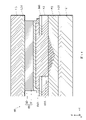
- FIG. 5 is an enlarged cross-sectional view of a main part schematically showing the configuration of the joint portion 60 shown in FIG. 4 and its surroundings.
- FIG. 5 is a cross section of a ZY plane in which the position of the X coordinate is different from the cross section shown in FIG.
- the Si substrate F2 is degenerate silicon (Si), and the Si substrate F2 itself also serves as a lower electrode of the resonator 10. Therefore, the above-mentioned metal layer E1 is not included.
- the joint portion 60 includes a eutectic layer 65 containing a eutectic alloy as a main component.
- the eutectic alloy of the eutectic layer 65 is, for example, a eutectic alloy of a first metal layer 61 containing aluminum (Al) as a main component and a second metal layer 62 of germanium (Ge).
- the first metal layer 61 and the second metal layer 62 are described as independent layers, but in reality, these interfaces are eutectic bonded. That is, the eutectic layer 65 is composed mainly of a eutectic alloy of a first metal containing aluminum (Al) as a main component and a second metal of germanium (Ge) as a main component. As described above, the joint portion 60 forms a eutectic alloy of the first metal of the first metal layer 61 containing aluminum (Al) as a main component and the second metal of the second metal layer 62 which is germanium (Ge). By including the eutectic layer 65 as a main component, it is possible to easily realize a bonded portion 60 having conductivity and high bonding strength.
- the first metal of the first metal layer 61 is composed of, for example, aluminum (Al), an aluminum-copper alloy (AlCu alloy), or an aluminum-silicon-copper alloy (AlSiCu alloy). Since aluminum or an aluminum alloy can be easily eutectic bonded to the germanium (Ge) of the second metal layer 62 and is a metal often used for wiring, for example, in a resonance device or the like, the manufacture of the resonance device 1 is performed. The process can be simplified, and the joint portion 60 for joining the MEMS substrate 50 and the upper lid 30 can be easily formed.
- the first metal of the first metal layer 61 is aluminum (Al)
- the second metal of the second metal layer 62 is germanium (Ge)
- the eutectic layer 65 is aluminum (Al)
- the eutectic layer 65 may contain aluminum (Al) and germanium (Ge) in addition to aluminum-germanium.
- a wiring layer 81 is provided on the parasitic capacitance reduction film 240 around the joint portion 60.
- the wiring layer 81 is configured to be electrically connected to the Si substrate F2 which has conductivity and functions as a lower electrode of the resonator 10.
- To form the wiring layer 81 first, a part of the parasitic capacitance reducing film 240 and the piezoelectric thin film F3 is removed, and holes are formed. Then, the hole is filled with a conductive material and electrically connected to the Si substrate F2.
- a diffusion prevention layer 85 is provided on the parasitic capacitance reduction film 240.
- the diffusion prevention layer 85 has conductivity and is configured to electrically connect the wiring layer 81 and the joint portion 60.
- the diffusion prevention layer 85 has a function of blocking and preventing the diffusion of the metal constituting the joint portion 60.
- the MEMS substrate 50 (resonant 10 and lower lid 20) includes the wiring layer 81 electrically connected to the Si substrate F2 which is the lower electrode of the resonator 10, so that the diffusion prevention layer 85 is interposed.
- the potential of the junction 60 can be reduced to the reference potential (GND) of the resonance device 1, and the generation of parasitic capacitance (stray capacitance) can be suppressed.
- the MEMS substrate 50 (resonator 10 and lower lid 20) includes the diffusion prevention layer 85 that electrically connects the wiring layer 81 and the bonding portion 60, the upper lid 30 and the MEMS substrate 50 are bonded.
- the diffusion prevention layer 85 can prevent the metal constituting the joint portion 60 from diffusing into the wiring layer 81. Therefore, it is possible to reduce the change in the metal ratio of the joint portion 60 due to diffusion, and it is possible to suppress the joint defect of the joint portion 60.
- the wiring layer 81 is formed at a position separated from the end portion of the joint portion 60.
- the wiring layer 81 is arranged on the MEMS substrate 50 (resonator 10 and lower lid 20) at a distance from the end portion of the joint portion 60. This makes it possible to arrange the diffusion prevention layer 85 between the joint portion 60 and the wiring layer 81. Therefore, the diffusion prevention layer 85 can be made thinner and the product cost of the resonance device 1 can be reduced as compared with the case where the diffusion prevention layer 85 is formed directly under the joint portion 60 described later.
- the material of the wiring layer 81 is preferably a metal containing aluminum (Al) as a main component.
- the metal containing aluminum (Al) as a main component is, for example, aluminum (Al), an aluminum-copper alloy (AlCu alloy), or an aluminum-silicon-copper alloy (AlSiCu alloy).
- the material of the wiring layer 81 is not limited to the case where it is a metal containing aluminum as a main component.
- the material of the wiring layer 81 may be a metal such as titanium (Ti).
- the wiring layer 81 is composed of a metal containing aluminum as a main component
- aluminum (Al) and silicon (Si) interact with each other at the interface between the wiring layer 81 and the Si substrate F2, as shown by the broken line in FIG. Diffuse, so-called alloy spikes, can occur.
- the silicon of the Si substrate F2 is in a state where it easily dissolves into the joint portion 60, and the role of the diffusion prevention layer 85 between the joint portion 60 and the joint portion 60 becomes even more important.
- the diffusion prevention layer 85 is composed of a metal having low diffusivity with respect to the metal of the joint portion 60.
- the material of the diffusion prevention layer 85 is preferably molybdenum (Mo) or tungsten (W), for example.
- Mo molybdenum
- W tungsten
- the material of the wiring layer 81 is aluminum (Al), and the material of the diffusion prevention layer 85 is molybdenum (Mo).
- FIG. 6 is a flowchart showing a manufacturing method of the resonance device 1 according to the embodiment.
- FIG. 7 is a cross-sectional view for explaining the process S301 shown in FIG.
- FIG. 8 is an enlarged cross-sectional view of a main part for explaining the first example of the step S302 shown in FIG.
- FIG. 9 is an enlarged cross-sectional view of a main part for explaining a second example of the step S302 shown in FIG.
- FIG. 10 is an enlarged cross-sectional view of a main part for explaining a third example of the step S302 shown in FIG. FIG.
- FIG. 11 is an enlarged cross-sectional view of a main part for explaining a fourth example of the step S302 shown in FIG.
- FIG. 12 is an enlarged cross-sectional view of a main part for explaining the process S303 shown in FIG.
- FIG. 13 is an enlarged cross-sectional view of a main part for explaining the step S304 shown in FIG. Note that FIGS. 7 to 13 show and describe one of the plurality of resonance devices 1 manufactured by the manufacturing method for convenience.
- the MEMS substrate 50 and the upper lid 30 are prepared (S301). Specifically, as shown in FIG. 7, the MEMS substrate 50 including the resonator 10 and the upper lid 30 described above are prepared. However, the connection wiring 70 shown in FIG. 4 for connecting the through electrode V3 and the resonator 10 has not yet been formed. Similarly, the joint portion 60, the wiring layer 81, and the diffusion prevention layer 85 shown in FIG. 5 have not yet been formed.
- the present invention is not limited to this.
- the MEMS substrate 50 and the upper lid 30 may be prepared separately for the process of preparing the MEMS substrate 50 and the process of preparing the upper lid 30.
- the first metal layer 61, the wiring layer 81, and the diffusion prevention layer 85 are formed on the MEMS substrate 50 prepared in the step S301 (S302).
- the parasitic capacitance reducing film 240 and the piezoelectric thin film F3 at predetermined positions are removed by etching or the like to form holes.
- the wiring layer 81 is formed by filling the holes formed with aluminum (Al) so as to be electrically connected to the Si substrate F2.
- molybdenum (Mo) is laminated on the ends of the parasitic capacitance reducing film 240 and the wiring layer 81, and the laminated molybdenum (Mo) is formed into a desired shape by etching or the like to form the laminated molybdenum (Mo) into a desired shape, thereby forming the diffusion prevention layer 85.
- the MEMS substrate 50 may be heat-treated for degassing at a high temperature, for example, about 435 ° C.
- the first metal layer 61 containing aluminum (Al) as a main component is less affected by heat diffusion even if it is heat-treated at a high temperature.
- FIG. 8 shows an example in which the first metal layer 61, the wiring layer 81, and the diffusion prevention layer 85 are formed on the MEMS substrate 50 in the order of the wiring layer 81, the diffusion prevention layer 85, and the first metal layer 61.
- Mo molybdenum
- a hole is formed at a predetermined position of the parasitic capacitance reducing film 240 to fill the hole with aluminum (Al), and aluminum (Al) is laminated on the ends of the parasitic capacitance reducing film 240 and the diffusion prevention layer 85.
- Al aluminum
- a hole is formed at a predetermined position of the parasitic capacitance reducing film 240, and the hole is filled with aluminum (Al).
- aluminum (Al) is laminated on the parasitic capacitance reducing film 240 to form the wiring layer 81 and the first metal layer 61, and then the parasitic capacitance reducing film 240, the end portion of the wiring layer 81, and Molybdenum (Mo) may be laminated on the end portion of the first metal layer 61 to form the anti-diffusion layer 85.
- the first metal layer 61 and the wiring layer 81 are formed on the upper layer or the lower layer of the diffusion prevention layer 85. can do. Therefore, the process of forming the first metal layer 61 and the wiring layer 81 can be reduced, and the manufacturing cost can be reduced.
- the diffusion prevention layer 85 may be composed of two or more layers.
- molybdenum (Mo) is laminated on the piezoelectric thin film F3 to form a metal layer E1 having a function as an upper electrode of the resonator 10 and a first layer 85a of the diffusion prevention layer 85.
- the parasitic capacitance reducing film 240 is laminated on the piezoelectric thin film F3 so as to cover the metal layer E1, and the protective film 235 is laminated at a predetermined position of the parasitic capacitance reducing film 240.
- molybdenum (Mo) is laminated on the first layer 85a at a predetermined position of the protective film 235 to form the frequency adjusting film 236 and the second layer 85b of the diffusion prevention layer 85. Then, a hole is formed at a predetermined position of the parasitic capacitance reducing film 240 to fill the hole with aluminum (Al), and aluminum (Al) is placed on the ends of the parasitic capacitance reducing film 240 and the diffusion prevention layer 85. By laminating, the wiring layer 81 and the first metal layer 61 are formed.
- the diffusion prevention layer 85 can be made thicker. It is possible to improve the blocking property that blocks the diffusion of the metal constituting the joint portion 60.
- the process S302 is not limited to the case where the process S302 is performed separately from the process S301.
- the formation of the first metal layer 61, the wiring layer 81, and the diffusion prevention layer 85 may be performed as a part of the step S301, or a part of the step of preparing the MEMS substrate 50 separated from the step S301. You may go as.
- the second metal layer 62 is formed on the upper lid 30 prepared in the step S301 (S303).
- germanium (Ge) is laminated on the surface of the silicon oxide film L31 on the back surface of the upper lid 30 to form the second metal layer 62 at a predetermined position.
- the predetermined position where the second metal layer 62 is formed is, for example, when the front surface of the MEMS substrate 50 and the back surface of the upper lid 30 face each other, the first metal formed on the MEMS substrate 50 on the back surface of the upper lid 30. It is a position facing or substantially facing the layer 61.
- the upper lid 30 is heat-treated for degassing at a high temperature, for example, about 435 ° C. As a result, the gas contained in the upper lid 30 and the second metal layer 62 can be sufficiently released (evaporated), and the generation of outgas can be reduced.
- the process S303 is not limited to the case where the process S303 is performed separately from the process S301.
- the formation of the second metal layer 62 may be performed as a part of the step S301, or may be performed as a part of the step of preparing the upper lid 30 separated from the step S301.
- a joint portion 60 including a eutectic layer 65 containing a eutectic alloy of a first metal containing aluminum (Al) as a main component and a second metal of germanium (Ge) as a main component is formed.
- the MEMS substrate 50 and the upper lid 30 are aligned so that the first metal layer 61 and the second metal layer 62 coincide with each other.
- the MEMS substrate 50 and the upper lid 30 are sandwiched by a heater or the like, and heat treatment for the eutectic reaction is performed.
- the upper lid 30 is moved toward the MEMS substrate 50.
- the second metal layer 62 comes into contact with the first metal layer 61.
- the temperature in the heat treatment for eutectic bonding is preferably the temperature of the confocal or higher and lower than the melting point of aluminum (Al) alone, that is, about 424 ° C or higher and lower than 620 ° C.
- the heating time is preferably about 10 minutes or more and 20 minutes or less.
- the heat treatment is performed at a temperature of 430 ° C. or higher and 500 ° C. or lower for about 15 minutes.
- the upper lid 30 and the MEMS substrate 50 are pressed from the upper lid 30 to the MEMS substrate 50 as shown by the black arrow in FIG.
- the pressure to be pressed is preferably about 5 MPa or more and 25 MPa or less.
- a cooling treatment is performed, for example, by natural cooling.
- the cooling treatment is not limited to natural cooling, as long as the eutectic layer 65 can be formed at the joint portion 60, and the cooling temperature and cooling speed thereof can be variously selected.
- a joint portion 60 including a eutectic layer 65 containing a eutectic alloy of a first metal and a second metal as a main component is formed.
- connection wiring 70 shown in FIG. 4 for connecting the through electrode V3 and the resonator 10 may be provided.
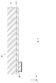
- the wiring layer 81 is arranged at a distance from the end portion of the joint portion 60 in the MEMS substrate 50, but the present invention is not limited to this.
- the position where the wiring layer 81 is formed and arranged can be appropriately changed.
- FIG. 14 is an enlarged cross-sectional view of a main part schematically showing a modified example of the configuration of the joint portion 60 and its surroundings shown in FIG.
- the same configurations as those of the joint portion 60 shown in FIG. 5 are designated by the same reference numerals, and the description thereof will be omitted as appropriate.
- similar actions and effects with the same configuration will not be mentioned sequentially.
- the wiring layer 81A and the diffusion prevention layer 85A may be provided under the joint portion 60, respectively.
- the wiring layer 81A is formed in a part around the vibrating portion 120 in the resonator 10.
- a diffusion prevention layer 85A is formed on the wiring layer 81A so as to cover the wiring layer 81A.
- the first metal layer 61 is formed on the diffusion prevention layer 85A.
- the eutectic layer 65 is formed by eutectic bonding the first metal layer 61 on the diffusion prevention layer 85A formed on the MEMS substrate 50 and the second metal layer 62 formed on the back surface of the upper lid 30 in this way.
- the including joint 60 is formed.
- the MEMS substrate comprises a wiring layer that is electrically connected to the lower electrode of the resonator.
- the potential of the junction can be reduced to the reference potential (GND) of the resonance device via the diffusion prevention layer, and the generation of parasitic capacitance (stray capacitance) can be suppressed.
- the MEMS substrate includes a diffusion prevention layer that electrically connects the wiring layer and the joint portion.
- the joint portion is a eutectic alloy of the first metal of the first metal layer containing aluminum (Al) as a main component and the second metal of the second metal layer which is germanium (Ge). Includes a eutectic layer whose main component is. As a result, it is possible to easily realize a joint portion having conductivity and high joint strength.
- the material of the diffusion prevention layer is molybdenum (Mo) or tungsten (W).
- the material of the Si substrate is degenerate silicon (Si).
- Si degenerate silicon
- the Si substrate itself can also serve as a lower electrode of the resonator.
- the material of the wiring layer is a metal containing aluminum (Al) as a main component. This makes it possible to remove (reduce) the oxide film formed on the surface of the Si substrate, which is the lower electrode of the resonator, by heat treatment at a relatively low temperature, for example, 450 ° C.
- the wiring layer is arranged on the MEMS substrate at a distance from the end portion of the joint portion. This makes it possible to arrange a diffusion prevention layer between the joint portion and the wiring layer. Therefore, as compared with the case where the diffusion prevention layer is formed directly under the joint portion, the diffusion prevention layer can be made thinner, and the product cost of the resonance device can be reduced.
- the first metal layer, the resonator, the wiring layer electrically connected to the Si substrate which is the lower electrode of the resonator, the wiring layer, and the first metal layer includes a step of preparing a MEMS substrate comprising an anti-diffusion layer for electrically connecting the two.
- the potential of the junction can be reduced to the reference potential (GND) of the resonance device via the diffusion prevention layer, and the generation of parasitic capacitance (stray capacitance) can be suppressed.
- the MEMS substrate includes a diffusion prevention layer that electrically connects the wiring layer and the joint portion.
- the metal constituting the joined portion can be prevented from diffusing into the wiring layer by the diffusion prevention layer. Therefore, it is possible to reduce the change in the metal ratio of the joint portion due to diffusion, and it is possible to suppress the joint failure of the joint portion.
- the step of preparing the MEMS substrate includes forming the first metal layer and the wiring layer before or after the formation of the diffusion prevention layer.
- the first metal layer and the wiring layer can be formed on the upper layer or the lower layer of the diffusion prevention layer. Therefore, the process of forming the first metal layer and the wiring layer can be reduced, and the manufacturing cost can be reduced.
- the steps of preparing the MEMS substrate include forming the first layer of the diffusion prevention layer, forming the second layer of the diffusion prevention layer on the first layer, and forming the second layer of the diffusion prevention layer. including.
- the diffusion prevention layer can be made thicker, and the blocking property for blocking the diffusion of the metal constituting the joint can be improved.
- the step of preparing a MEMS substrate includes forming a wiring layer at a position at a distance from the end of the joint portion in the MEMS substrate. This makes it possible to arrange a diffusion prevention layer between the joint portion and the wiring layer. Therefore, as compared with the case where the diffusion prevention layer is formed directly under the joint portion, the diffusion prevention layer can be made thinner, and the product cost of the resonance device can be reduced.
- the first metal of the first metal layer is a metal containing aluminum (Al) as a main component
- the second metal of the second metal layer is germanium (Ge).
- the material of the diffusion prevention layer is molybdenum (Mo) or tungsten (W).
- the material of the Si substrate is degenerate silicon (Si).
- Si degenerate silicon
- the Si substrate itself can also serve as a lower electrode of the resonator.
- the material of the wiring layer is a metal containing aluminum (Al) as a main component. This makes it possible to remove (reduce) the oxide film formed on the surface of the Si substrate, which is the lower electrode of the resonator, by heat treatment at a relatively low temperature, for example, 450 ° C.
- Base 131a ... Long side, 131A ... Front end, 131b ... Long side, 131B ... Rear end, 131c ... short side, 131d ... short side, 135, 135A, 135B, 135C, 135D ... vibrating arm, 140 holding part, 141 ... voltage application part, 235 ... protective film, 236 ... frequency adjustment film, 240 ... parasitic capacity reduction film, E1 ... metal layer, E2 ... metal layer, F2 ... Si substrate, F3 ... piezoelectric thin film, F21 ... silicon oxide layer, G ... weight part, L1 ... Si wafer, L3 ... Si substrate, L31 ... silicon oxide film, P ... virtual Flat surface, T4 ... terminal, V1 ... via, V2 ... via, V3 ... through electrode.
Landscapes
- Engineering & Computer Science (AREA)
- Manufacturing & Machinery (AREA)
- Physics & Mathematics (AREA)
- Acoustics & Sound (AREA)
- Mechanical Engineering (AREA)
- Microelectronics & Electronic Packaging (AREA)
- Piezo-Electric Or Mechanical Vibrators, Or Delay Or Filter Circuits (AREA)
- Micromachines (AREA)
Priority Applications (3)
| Application Number | Priority Date | Filing Date | Title |
|---|---|---|---|
| CN202180063936.7A CN116133782B (zh) | 2020-11-06 | 2021-07-02 | 谐振装置以及谐振装置制造方法 |
| JP2022560644A JP7493709B2 (ja) | 2020-11-06 | 2021-07-02 | 共振装置及び共振装置製造方法 |
| US18/175,954 US20230208392A1 (en) | 2020-11-06 | 2023-02-28 | Resonance device and resonance device manufacturing method |
Applications Claiming Priority (2)
| Application Number | Priority Date | Filing Date | Title |
|---|---|---|---|
| JP2020185834 | 2020-11-06 | ||
| JP2020-185834 | 2020-11-06 |
Related Child Applications (1)
| Application Number | Title | Priority Date | Filing Date |
|---|---|---|---|
| US18/175,954 Continuation US20230208392A1 (en) | 2020-11-06 | 2023-02-28 | Resonance device and resonance device manufacturing method |
Publications (1)
| Publication Number | Publication Date |
|---|---|
| WO2022097328A1 true WO2022097328A1 (ja) | 2022-05-12 |
Family
ID=81457684
Family Applications (1)
| Application Number | Title | Priority Date | Filing Date |
|---|---|---|---|
| PCT/JP2021/025075 Ceased WO2022097328A1 (ja) | 2020-11-06 | 2021-07-02 | 共振装置及び共振装置製造方法 |
Country Status (4)
| Country | Link |
|---|---|
| US (1) | US20230208392A1 (https=) |
| JP (1) | JP7493709B2 (https=) |
| CN (1) | CN116133782B (https=) |
| WO (1) | WO2022097328A1 (https=) |
Families Citing this family (1)
| Publication number | Priority date | Publication date | Assignee | Title |
|---|---|---|---|---|
| FI131276B1 (en) * | 2023-07-17 | 2025-01-22 | Kyocera Tech Oy | IMPLEMENTATIONS TO SILICON |
Citations (3)
| Publication number | Priority date | Publication date | Assignee | Title |
|---|---|---|---|---|
| WO2011111541A1 (ja) * | 2010-03-09 | 2011-09-15 | アルプス電気株式会社 | Memsセンサ |
| WO2019155663A1 (ja) * | 2018-02-09 | 2019-08-15 | 株式会社村田製作所 | Memsデバイス |
| WO2020085188A1 (ja) * | 2018-10-24 | 2020-04-30 | 株式会社村田製作所 | 共振装置 |
Family Cites Families (13)
| Publication number | Priority date | Publication date | Assignee | Title |
|---|---|---|---|---|
| JP4086023B2 (ja) * | 2003-12-04 | 2008-05-14 | セイコーエプソン株式会社 | マイクロメカニカル静電振動子 |
| JP4458203B2 (ja) * | 2007-12-06 | 2010-04-28 | 株式会社村田製作所 | 圧電振動部品 |
| JP6163832B2 (ja) * | 2013-03-29 | 2017-07-19 | セイコーエプソン株式会社 | 振動片、振動片の製造方法、振動子、発振器、電子機器および移動体 |
| JP2017130823A (ja) * | 2016-01-21 | 2017-07-27 | 京セラ株式会社 | 圧電発振器及びその製造方法 |
| WO2018008198A1 (ja) * | 2016-07-05 | 2018-01-11 | 株式会社村田製作所 | 共振子及び共振装置 |
| WO2019111740A1 (ja) * | 2017-12-06 | 2019-06-13 | 株式会社村田製作所 | 電子部品 |
| WO2019159410A1 (ja) * | 2018-02-14 | 2019-08-22 | 株式会社村田製作所 | 共振装置及び共振装置製造方法 |
| CN112335178B (zh) * | 2018-08-02 | 2024-02-13 | 株式会社村田制作所 | Mems设备 |
| JP7047922B2 (ja) * | 2018-09-04 | 2022-04-05 | 株式会社村田製作所 | Memsデバイスの製造方法及びmemsデバイス |
| CN112689957B (zh) * | 2018-09-28 | 2024-05-14 | 株式会社村田制作所 | 共振装置和共振装置的制造方法 |
| CN113491069B (zh) * | 2019-03-26 | 2024-05-28 | 株式会社村田制作所 | 谐振装置和谐振装置制造方法 |
| CN113632375A (zh) * | 2019-06-19 | 2021-11-09 | 株式会社村田制作所 | 谐振装置以及谐振装置制造方法 |
| JP7154487B2 (ja) * | 2019-09-05 | 2022-10-18 | 株式会社村田製作所 | パッケージ構造及びその製造方法 |
-
2021
- 2021-07-02 JP JP2022560644A patent/JP7493709B2/ja active Active
- 2021-07-02 WO PCT/JP2021/025075 patent/WO2022097328A1/ja not_active Ceased
- 2021-07-02 CN CN202180063936.7A patent/CN116133782B/zh active Active
-
2023
- 2023-02-28 US US18/175,954 patent/US20230208392A1/en active Pending
Patent Citations (3)
| Publication number | Priority date | Publication date | Assignee | Title |
|---|---|---|---|---|
| WO2011111541A1 (ja) * | 2010-03-09 | 2011-09-15 | アルプス電気株式会社 | Memsセンサ |
| WO2019155663A1 (ja) * | 2018-02-09 | 2019-08-15 | 株式会社村田製作所 | Memsデバイス |
| WO2020085188A1 (ja) * | 2018-10-24 | 2020-04-30 | 株式会社村田製作所 | 共振装置 |
Also Published As
| Publication number | Publication date |
|---|---|
| US20230208392A1 (en) | 2023-06-29 |
| JPWO2022097328A1 (https=) | 2022-05-12 |
| CN116133782A (zh) | 2023-05-16 |
| JP7493709B2 (ja) | 2024-06-03 |
| CN116133782B (zh) | 2026-03-13 |
Similar Documents
| Publication | Publication Date | Title |
|---|---|---|
| JP6923010B2 (ja) | Memsデバイス | |
| JP7265729B2 (ja) | 共振装置及び共振装置製造方法 | |
| US11757425B2 (en) | Resonance device and method for producing resonance device | |
| JP7015484B2 (ja) | Memsデバイス | |
| US11881838B2 (en) | Resonance device and manufacturing method of resonance device | |
| CN112585870B (zh) | 谐振装置 | |
| CN114342067B (zh) | 封装结构及其制造方法 | |
| US20230119602A1 (en) | Resonance device, collective substrate, and resonance device manufacturing method | |
| US12365583B2 (en) | Resonance device with substrate having oxide film containing through hole and metal therin, and manufacturing method therefor | |
| US20230208392A1 (en) | Resonance device and resonance device manufacturing method | |
| WO2021205685A1 (ja) | 集合基板の製造方法及び集合基板 | |
| US12531539B2 (en) | Resonance device, collective board, and method of manufacturing resonance device | |
| JP7680716B2 (ja) | 共振装置及び共振装置の製造方法 |
Legal Events
| Date | Code | Title | Description |
|---|---|---|---|
| 121 | Ep: the epo has been informed by wipo that ep was designated in this application |
Ref document number: 21888881 Country of ref document: EP Kind code of ref document: A1 |
|
| ENP | Entry into the national phase |
Ref document number: 2022560644 Country of ref document: JP Kind code of ref document: A |
|
| NENP | Non-entry into the national phase |
Ref country code: DE |
|
| 122 | Ep: pct application non-entry in european phase |
Ref document number: 21888881 Country of ref document: EP Kind code of ref document: A1 |