WO2022097328A1 - Resonance device and resonance device manufacturing method - Google Patents
Resonance device and resonance device manufacturing method Download PDFInfo
- Publication number
- WO2022097328A1 WO2022097328A1 PCT/JP2021/025075 JP2021025075W WO2022097328A1 WO 2022097328 A1 WO2022097328 A1 WO 2022097328A1 JP 2021025075 W JP2021025075 W JP 2021025075W WO 2022097328 A1 WO2022097328 A1 WO 2022097328A1
- Authority
- WO
- WIPO (PCT)
- Prior art keywords
- layer
- resonator
- substrate
- metal
- metal layer
- Prior art date
Links
- 238000004519 manufacturing process Methods 0.000 title claims abstract description 28
- 239000000758 substrate Substances 0.000 claims abstract description 122
- 238000009792 diffusion process Methods 0.000 claims abstract description 80
- 230000002265 prevention Effects 0.000 claims abstract description 66
- 229910052751 metal Inorganic materials 0.000 claims description 156
- 239000002184 metal Substances 0.000 claims description 156
- 238000000034 method Methods 0.000 claims description 44
- 229910052782 aluminium Inorganic materials 0.000 claims description 41
- XAGFODPZIPBFFR-UHFFFAOYSA-N aluminium Chemical compound [Al] XAGFODPZIPBFFR-UHFFFAOYSA-N 0.000 claims description 41
- 230000005496 eutectics Effects 0.000 claims description 30
- 230000008569 process Effects 0.000 claims description 24
- 239000000463 material Substances 0.000 claims description 23
- 229910052732 germanium Inorganic materials 0.000 claims description 17
- GNPVGFCGXDBREM-UHFFFAOYSA-N germanium atom Chemical compound [Ge] GNPVGFCGXDBREM-UHFFFAOYSA-N 0.000 claims description 17
- 229910052710 silicon Inorganic materials 0.000 claims description 17
- 239000010703 silicon Substances 0.000 claims description 17
- ZOKXTWBITQBERF-UHFFFAOYSA-N Molybdenum Chemical group [Mo] ZOKXTWBITQBERF-UHFFFAOYSA-N 0.000 claims description 13
- 239000006023 eutectic alloy Substances 0.000 claims description 13
- 238000005304 joining Methods 0.000 claims description 13
- 229910052750 molybdenum Inorganic materials 0.000 claims description 13
- 239000011733 molybdenum Substances 0.000 claims description 13
- 230000015572 biosynthetic process Effects 0.000 claims description 7
- WFKWXMTUELFFGS-UHFFFAOYSA-N tungsten Chemical compound [W] WFKWXMTUELFFGS-UHFFFAOYSA-N 0.000 claims description 7
- 229910052721 tungsten Inorganic materials 0.000 claims description 7
- 239000010937 tungsten Substances 0.000 claims description 7
- 230000007547 defect Effects 0.000 abstract description 5
- 239000010408 film Substances 0.000 description 64
- 230000003071 parasitic effect Effects 0.000 description 28
- 230000001681 protective effect Effects 0.000 description 19
- 239000010409 thin film Substances 0.000 description 19
- XUIMIQQOPSSXEZ-UHFFFAOYSA-N Silicon Chemical compound [Si] XUIMIQQOPSSXEZ-UHFFFAOYSA-N 0.000 description 15
- VYPSYNLAJGMNEJ-UHFFFAOYSA-N Silicium dioxide Chemical compound O=[Si]=O VYPSYNLAJGMNEJ-UHFFFAOYSA-N 0.000 description 14
- 238000005530 etching Methods 0.000 description 9
- 238000010438 heat treatment Methods 0.000 description 9
- 230000009467 reduction Effects 0.000 description 9
- 229910052814 silicon oxide Inorganic materials 0.000 description 8
- 229910045601 alloy Inorganic materials 0.000 description 7
- 239000000956 alloy Substances 0.000 description 7
- 238000001816 cooling Methods 0.000 description 6
- 239000010931 gold Substances 0.000 description 6
- 239000010936 titanium Substances 0.000 description 6
- 230000008859 change Effects 0.000 description 5
- 229910000881 Cu alloy Inorganic materials 0.000 description 4
- -1 aluminum-silicon-copper Chemical compound 0.000 description 4
- 230000000903 blocking effect Effects 0.000 description 4
- 239000011777 magnesium Substances 0.000 description 4
- PXHVJJICTQNCMI-UHFFFAOYSA-N Nickel Chemical compound [Ni] PXHVJJICTQNCMI-UHFFFAOYSA-N 0.000 description 3
- 229910004298 SiO 2 Inorganic materials 0.000 description 3
- RTAQQCXQSZGOHL-UHFFFAOYSA-N Titanium Chemical compound [Ti] RTAQQCXQSZGOHL-UHFFFAOYSA-N 0.000 description 3
- 238000005452 bending Methods 0.000 description 3
- 239000004020 conductor Substances 0.000 description 3
- 230000005684 electric field Effects 0.000 description 3
- PCHJSUWPFVWCPO-UHFFFAOYSA-N gold Chemical compound [Au] PCHJSUWPFVWCPO-UHFFFAOYSA-N 0.000 description 3
- 229910052737 gold Inorganic materials 0.000 description 3
- BASFCYQUMIYNBI-UHFFFAOYSA-N platinum Chemical compound [Pt] BASFCYQUMIYNBI-UHFFFAOYSA-N 0.000 description 3
- 235000012239 silicon dioxide Nutrition 0.000 description 3
- 239000000377 silicon dioxide Substances 0.000 description 3
- 229910052719 titanium Inorganic materials 0.000 description 3
- 229910016570 AlCu Inorganic materials 0.000 description 2
- PIGFYZPCRLYGLF-UHFFFAOYSA-N Aluminum nitride Chemical compound [Al]#N PIGFYZPCRLYGLF-UHFFFAOYSA-N 0.000 description 2
- XKRFYHLGVUSROY-UHFFFAOYSA-N Argon Chemical compound [Ar] XKRFYHLGVUSROY-UHFFFAOYSA-N 0.000 description 2
- JMASRVWKEDWRBT-UHFFFAOYSA-N Gallium nitride Chemical compound [Ga]#N JMASRVWKEDWRBT-UHFFFAOYSA-N 0.000 description 2
- FYYHWMGAXLPEAU-UHFFFAOYSA-N Magnesium Chemical compound [Mg] FYYHWMGAXLPEAU-UHFFFAOYSA-N 0.000 description 2
- 229910052581 Si3N4 Inorganic materials 0.000 description 2
- BOTDANWDWHJENH-UHFFFAOYSA-N Tetraethyl orthosilicate Chemical compound CCO[Si](OCC)(OCC)OCC BOTDANWDWHJENH-UHFFFAOYSA-N 0.000 description 2
- XLOMVQKBTHCTTD-UHFFFAOYSA-N Zinc monoxide Chemical compound [Zn]=O XLOMVQKBTHCTTD-UHFFFAOYSA-N 0.000 description 2
- WPPDFTBPZNZZRP-UHFFFAOYSA-N aluminum copper Chemical compound [Al].[Cu] WPPDFTBPZNZZRP-UHFFFAOYSA-N 0.000 description 2
- NWAIGJYBQQYSPW-UHFFFAOYSA-N azanylidyneindigane Chemical compound [In]#N NWAIGJYBQQYSPW-UHFFFAOYSA-N 0.000 description 2
- CUOITRGULIVMPC-UHFFFAOYSA-N azanylidynescandium Chemical compound [Sc]#N CUOITRGULIVMPC-UHFFFAOYSA-N 0.000 description 2
- 238000006243 chemical reaction Methods 0.000 description 2
- 238000005229 chemical vapour deposition Methods 0.000 description 2
- 239000010949 copper Substances 0.000 description 2
- PMHQVHHXPFUNSP-UHFFFAOYSA-M copper(1+);methylsulfanylmethane;bromide Chemical compound Br[Cu].CSC PMHQVHHXPFUNSP-UHFFFAOYSA-M 0.000 description 2
- 239000013078 crystal Substances 0.000 description 2
- 238000007872 degassing Methods 0.000 description 2
- 238000005516 engineering process Methods 0.000 description 2
- 238000010030 laminating Methods 0.000 description 2
- 229910052749 magnesium Inorganic materials 0.000 description 2
- 230000004048 modification Effects 0.000 description 2
- 238000012986 modification Methods 0.000 description 2
- 150000002751 molybdenum Chemical class 0.000 description 2
- 239000010955 niobium Substances 0.000 description 2
- 230000003647 oxidation Effects 0.000 description 2
- 238000007254 oxidation reaction Methods 0.000 description 2
- 230000002093 peripheral effect Effects 0.000 description 2
- 229910021420 polycrystalline silicon Inorganic materials 0.000 description 2
- 229920005591 polysilicon Polymers 0.000 description 2
- 229910052706 scandium Inorganic materials 0.000 description 2
- SIXSYDAISGFNSX-UHFFFAOYSA-N scandium atom Chemical group [Sc] SIXSYDAISGFNSX-UHFFFAOYSA-N 0.000 description 2
- HQVNEWCFYHHQES-UHFFFAOYSA-N silicon nitride Chemical compound N12[Si]34N5[Si]62N3[Si]51N64 HQVNEWCFYHHQES-UHFFFAOYSA-N 0.000 description 2
- 229910018072 Al 2 O 3 Inorganic materials 0.000 description 1
- 229910000838 Al alloy Inorganic materials 0.000 description 1
- RYGMFSIKBFXOCR-UHFFFAOYSA-N Copper Chemical compound [Cu] RYGMFSIKBFXOCR-UHFFFAOYSA-N 0.000 description 1
- 235000019687 Lamb Nutrition 0.000 description 1
- OAICVXFJPJFONN-UHFFFAOYSA-N Phosphorus Chemical compound [P] OAICVXFJPJFONN-UHFFFAOYSA-N 0.000 description 1
- ATJFFYVFTNAWJD-UHFFFAOYSA-N Tin Chemical compound [Sn] ATJFFYVFTNAWJD-UHFFFAOYSA-N 0.000 description 1
- 230000001133 acceleration Effects 0.000 description 1
- AZDRQVAHHNSJOQ-UHFFFAOYSA-N alumane Chemical class [AlH3] AZDRQVAHHNSJOQ-UHFFFAOYSA-N 0.000 description 1
- PNEYBMLMFCGWSK-UHFFFAOYSA-N aluminium oxide Inorganic materials [O-2].[O-2].[O-2].[Al+3].[Al+3] PNEYBMLMFCGWSK-UHFFFAOYSA-N 0.000 description 1
- 229910052787 antimony Inorganic materials 0.000 description 1
- WATWJIUSRGPENY-UHFFFAOYSA-N antimony atom Chemical compound [Sb] WATWJIUSRGPENY-UHFFFAOYSA-N 0.000 description 1
- 229910052786 argon Inorganic materials 0.000 description 1
- 229910052785 arsenic Inorganic materials 0.000 description 1
- RQNWIZPPADIBDY-UHFFFAOYSA-N arsenic atom Chemical compound [As] RQNWIZPPADIBDY-UHFFFAOYSA-N 0.000 description 1
- 230000008602 contraction Effects 0.000 description 1
- 229910052802 copper Inorganic materials 0.000 description 1
- 238000012937 correction Methods 0.000 description 1
- 238000013461 design Methods 0.000 description 1
- 239000002019 doping agent Substances 0.000 description 1
- 238000001312 dry etching Methods 0.000 description 1
- 230000000694 effects Effects 0.000 description 1
- 239000007789 gas Substances 0.000 description 1
- 238000010884 ion-beam technique Methods 0.000 description 1
- 230000008018 melting Effects 0.000 description 1
- 238000002844 melting Methods 0.000 description 1
- 150000002739 metals Chemical class 0.000 description 1
- 229910021421 monocrystalline silicon Inorganic materials 0.000 description 1
- 229910052759 nickel Inorganic materials 0.000 description 1
- 229910052758 niobium Inorganic materials 0.000 description 1
- GUCVJGMIXFAOAE-UHFFFAOYSA-N niobium atom Chemical compound [Nb] GUCVJGMIXFAOAE-UHFFFAOYSA-N 0.000 description 1
- 150000004767 nitrides Chemical class 0.000 description 1
- 238000000059 patterning Methods 0.000 description 1
- 229910052698 phosphorus Inorganic materials 0.000 description 1
- 239000011574 phosphorus Substances 0.000 description 1
- 229910052697 platinum Inorganic materials 0.000 description 1
- 238000012545 processing Methods 0.000 description 1
- 238000007789 sealing Methods 0.000 description 1
- VSZWPYCFIRKVQL-UHFFFAOYSA-N selanylidenegallium;selenium Chemical compound [Se].[Se]=[Ga].[Se]=[Ga] VSZWPYCFIRKVQL-UHFFFAOYSA-N 0.000 description 1
- 239000004065 semiconductor Substances 0.000 description 1
- 238000006467 substitution reaction Methods 0.000 description 1
Images


Classifications
-
- H—ELECTRICITY
- H03—ELECTRONIC CIRCUITRY
- H03H—IMPEDANCE NETWORKS, e.g. RESONANT CIRCUITS; RESONATORS
- H03H9/00—Networks comprising electromechanical or electro-acoustic devices; Electromechanical resonators
- H03H9/02—Details
- H03H9/05—Holders; Supports
- H03H9/10—Mounting in enclosures
- H03H9/1057—Mounting in enclosures for microelectro-mechanical devices
-
- H—ELECTRICITY
- H03—ELECTRONIC CIRCUITRY
- H03H—IMPEDANCE NETWORKS, e.g. RESONANT CIRCUITS; RESONATORS
- H03H9/00—Networks comprising electromechanical or electro-acoustic devices; Electromechanical resonators
- H03H9/15—Constructional features of resonators consisting of piezoelectric or electrostrictive material
- H03H9/17—Constructional features of resonators consisting of piezoelectric or electrostrictive material having a single resonator
- H03H9/171—Constructional features of resonators consisting of piezoelectric or electrostrictive material having a single resonator implemented with thin-film techniques, i.e. of the film bulk acoustic resonator [FBAR] type
-
- B—PERFORMING OPERATIONS; TRANSPORTING
- B23—MACHINE TOOLS; METAL-WORKING NOT OTHERWISE PROVIDED FOR
- B23K—SOLDERING OR UNSOLDERING; WELDING; CLADDING OR PLATING BY SOLDERING OR WELDING; CUTTING BY APPLYING HEAT LOCALLY, e.g. FLAME CUTTING; WORKING BY LASER BEAM
- B23K20/00—Non-electric welding by applying impact or other pressure, with or without the application of heat, e.g. cladding or plating
- B23K20/002—Non-electric welding by applying impact or other pressure, with or without the application of heat, e.g. cladding or plating specially adapted for particular articles or work
- B23K20/004—Wire welding
-
- B—PERFORMING OPERATIONS; TRANSPORTING
- B23—MACHINE TOOLS; METAL-WORKING NOT OTHERWISE PROVIDED FOR
- B23K—SOLDERING OR UNSOLDERING; WELDING; CLADDING OR PLATING BY SOLDERING OR WELDING; CUTTING BY APPLYING HEAT LOCALLY, e.g. FLAME CUTTING; WORKING BY LASER BEAM
- B23K20/00—Non-electric welding by applying impact or other pressure, with or without the application of heat, e.g. cladding or plating
- B23K20/02—Non-electric welding by applying impact or other pressure, with or without the application of heat, e.g. cladding or plating by means of a press ; Diffusion bonding
-
- B—PERFORMING OPERATIONS; TRANSPORTING
- B23—MACHINE TOOLS; METAL-WORKING NOT OTHERWISE PROVIDED FOR
- B23K—SOLDERING OR UNSOLDERING; WELDING; CLADDING OR PLATING BY SOLDERING OR WELDING; CUTTING BY APPLYING HEAT LOCALLY, e.g. FLAME CUTTING; WORKING BY LASER BEAM
- B23K20/00—Non-electric welding by applying impact or other pressure, with or without the application of heat, e.g. cladding or plating
- B23K20/18—Zonal welding by interposing weld-preventing substances between zones not to be welded
-
- B—PERFORMING OPERATIONS; TRANSPORTING
- B81—MICROSTRUCTURAL TECHNOLOGY
- B81C—PROCESSES OR APPARATUS SPECIALLY ADAPTED FOR THE MANUFACTURE OR TREATMENT OF MICROSTRUCTURAL DEVICES OR SYSTEMS
- B81C3/00—Assembling of devices or systems from individually processed components
- B81C3/001—Bonding of two components
-
- H—ELECTRICITY
- H03—ELECTRONIC CIRCUITRY
- H03H—IMPEDANCE NETWORKS, e.g. RESONANT CIRCUITS; RESONATORS
- H03H3/00—Apparatus or processes specially adapted for the manufacture of impedance networks, resonating circuits, resonators
- H03H3/007—Apparatus or processes specially adapted for the manufacture of impedance networks, resonating circuits, resonators for the manufacture of electromechanical resonators or networks
- H03H3/0072—Apparatus or processes specially adapted for the manufacture of impedance networks, resonating circuits, resonators for the manufacture of electromechanical resonators or networks of microelectro-mechanical resonators or networks
-
- H—ELECTRICITY
- H03—ELECTRONIC CIRCUITRY
- H03H—IMPEDANCE NETWORKS, e.g. RESONANT CIRCUITS; RESONATORS
- H03H3/00—Apparatus or processes specially adapted for the manufacture of impedance networks, resonating circuits, resonators
- H03H3/007—Apparatus or processes specially adapted for the manufacture of impedance networks, resonating circuits, resonators for the manufacture of electromechanical resonators or networks
- H03H3/02—Apparatus or processes specially adapted for the manufacture of impedance networks, resonating circuits, resonators for the manufacture of electromechanical resonators or networks for the manufacture of piezoelectric or electrostrictive resonators or networks
-
- H—ELECTRICITY
- H03—ELECTRONIC CIRCUITRY
- H03H—IMPEDANCE NETWORKS, e.g. RESONANT CIRCUITS; RESONATORS
- H03H9/00—Networks comprising electromechanical or electro-acoustic devices; Electromechanical resonators
- H03H9/24—Constructional features of resonators of material which is not piezoelectric, electrostrictive, or magnetostrictive
- H03H9/2405—Constructional features of resonators of material which is not piezoelectric, electrostrictive, or magnetostrictive of microelectro-mechanical resonators
- H03H9/2468—Tuning fork resonators
- H03H9/2478—Single-Ended Tuning Fork resonators
- H03H9/2489—Single-Ended Tuning Fork resonators with more than two fork tines
-
- B—PERFORMING OPERATIONS; TRANSPORTING
- B81—MICROSTRUCTURAL TECHNOLOGY
- B81B—MICROSTRUCTURAL DEVICES OR SYSTEMS, e.g. MICROMECHANICAL DEVICES
- B81B2201/00—Specific applications of microelectromechanical systems
- B81B2201/02—Sensors
- B81B2201/0271—Resonators; ultrasonic resonators
-
- B—PERFORMING OPERATIONS; TRANSPORTING
- B81—MICROSTRUCTURAL TECHNOLOGY
- B81B—MICROSTRUCTURAL DEVICES OR SYSTEMS, e.g. MICROMECHANICAL DEVICES
- B81B2201/00—Specific applications of microelectromechanical systems
- B81B2201/03—Microengines and actuators
- B81B2201/032—Bimorph and unimorph actuators, e.g. piezo and thermo
-
- B—PERFORMING OPERATIONS; TRANSPORTING
- B81—MICROSTRUCTURAL TECHNOLOGY
- B81B—MICROSTRUCTURAL DEVICES OR SYSTEMS, e.g. MICROMECHANICAL DEVICES
- B81B2207/00—Microstructural systems or auxiliary parts thereof
- B81B2207/07—Interconnects
-
- B—PERFORMING OPERATIONS; TRANSPORTING
- B81—MICROSTRUCTURAL TECHNOLOGY
- B81C—PROCESSES OR APPARATUS SPECIALLY ADAPTED FOR THE MANUFACTURE OR TREATMENT OF MICROSTRUCTURAL DEVICES OR SYSTEMS
- B81C2203/00—Forming microstructural systems
- B81C2203/03—Bonding two components
- B81C2203/033—Thermal bonding
- B81C2203/035—Soldering
Definitions
- the present invention relates to a resonance device and a method for manufacturing a resonance device.
- a resonance device manufactured by using MEMS Micro Electro Mechanical Systems
- This device is formed by joining an upper substrate to, for example, a lower substrate having a resonator.
- Patent Document 1 includes a lower substrate having a resonator, an upper substrate provided facing the element, and a joint portion for joining the lower substrate and the upper substrate around the element.
- a MEMS device having a region containing a hypereutectic alloy and a region containing a eutectic alloy is disclosed as a junction.
- the hypereutectic alloy covers the eutectic alloy to prevent the metal from squeezing out from the joint surface of the eutectic joint.
- the characteristics of the MEMS device may be improved by connecting the joint portion to the ground (GND) to suppress the generation of parasitic capacitance (stray capacitance).
- the joint and the lower electrode of the resonator were connected by an aluminum (Al) wiring having good electrical connectivity.
- the metal constituting the joining portion for example, germanium (Ge)
- the metal constituting the joining portion diffuses into the aluminum wiring and flows into the lower electrode side of the resonator. Therefore, the ratio of the metals constituting the joint portion may change, the eutectic ratio (eutectic ratio) may change, or the eutectic reaction may become insufficient.
- joint defects such as a decrease in the joint strength of the joint portion occur.
- the present invention has been made in view of such circumstances, and one of the objects of the present invention is to provide a resonance device and a method for manufacturing a resonance device capable of suppressing joint defects in a joint portion.
- the resonance device includes a first substrate including a resonator, a second substrate, and a joint portion having conductivity and joining the first substrate and the second substrate.
- One substrate further includes a wiring layer that is electrically connected to the lower electrode of the resonator and a diffusion prevention layer that electrically connects the wiring layer and the joint portion.
- a method for manufacturing a resonator according to another aspect of the present invention includes a first metal layer, a resonator, a wiring layer electrically connected to a lower electrode of the resonator, and the wiring layer and the first metal layer.
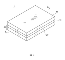
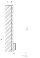
- FIG. 1 is a perspective view schematically showing the appearance of the resonance device according to the embodiment of the present invention.
- FIG. 2 is an exploded perspective view schematically showing the structure of the resonance apparatus shown in FIG.
- FIG. 3 is a plan view schematically showing the structure of the resonator shown in FIG.
- FIG. 4 is a cross-sectional view schematically showing the configuration of a cross section of the resonator shown in FIGS. 1 to 3 along the IV-IV line.
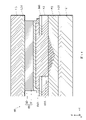
- FIG. 5 is an enlarged cross-sectional view of a main part schematically showing the configuration of the joint portion shown in FIG. 4 and its surroundings.
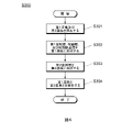
- FIG. 6 is a flowchart showing a method of manufacturing a resonance device according to an embodiment.
- FIG. 7 is a cross-sectional view for explaining the process shown in FIG.
- FIG. 8 is an enlarged cross-sectional view of a main part for explaining the first example of the process shown in FIG.
- FIG. 9 is an enlarged cross-sectional view of a main part for explaining a second example of the process shown in FIG.
- FIG. 10 is an enlarged cross-sectional view of a main part for explaining a third example of the process shown in FIG.
- FIG. 11 is an enlarged cross-sectional view of a main part for explaining a fourth example of the process shown in FIG.
- FIG. 12 is an enlarged cross-sectional view of a main part for explaining the process shown in FIG.
- FIG. 13 is an enlarged plan view of a main part for explaining the process shown in FIG.
- FIG. 14 is an enlarged cross-sectional view of a main part showing a third modification of the joint portion shown in FIG.
- FIG. 1 is a perspective view schematically showing the appearance of the resonance device 1 in one embodiment.
- FIG. 2 is an exploded perspective view schematically showing the structure of the resonance device 1 shown in FIG.
- the resonator 1 includes a lower lid 20, a resonator 10 (hereinafter, the lower lid 20 and the resonator 10 are collectively referred to as a “MEMS substrate 50”), and an upper lid 30. That is, the resonator 1 is configured by laminating the MEMS substrate 50, the joint portion 60, and the upper lid 30 in this order.
- the MEMS substrate 50 corresponds to an example of the "first substrate” of the present invention
- the upper lid 30 corresponds to an example of the "second substrate” of the present invention.
- the side of the resonance device 1 where the upper lid 30 is provided is referred to as the upper side (or the front side), and the side where the lower lid 20 is provided is referred to as the lower side (or the back side).
- the resonator 10 is a MEMS oscillator manufactured using MEMS technology.
- the resonator 10 and the upper lid 30 are joined via a joint portion 60, which will be described later.
- the resonator 10 and the lower lid 20 are each formed of a silicon (Si) substrate (hereinafter referred to as “Si substrate”), and the Si substrates are bonded to each other.
- the MEMS substrate 50 (resonator 10 and lower lid 20) may be formed by using an SOI substrate.
- the upper lid 30 extends in a flat plate shape along the XY plane, and for example, a flat rectangular parallelepiped concave portion 31 is formed on the back surface thereof.
- the recess 31 is surrounded by the side wall 33 and forms a part of the vibration space, which is the space where the resonator 10 vibrates.
- a getter layer 34 which will be described later, is formed on the surface of the concave portion 31 of the upper lid 30 on the resonator 10 side.
- the upper lid 30 does not have a recess 31, and may have a flat plate shape.
- the lower lid 20 includes a rectangular flat plate-shaped bottom plate 22 provided along the XY plane, and a side wall 23 extending in the Z-axis direction from the peripheral edge of the bottom plate 22, that is, in the stacking direction of the lower lid 20 and the resonator 10.
- the lower lid 20 is formed with a recess 21 formed by the surface of the bottom plate 22 and the inner surface of the side wall 23 on the surface facing the resonator 10.
- the recess 21 forms a part of the vibration space of the resonator 10.
- the lower lid 20 does not have the recess 21 and may have a flat plate shape. Further, a getter layer may be formed on the surface of the lower lid 20 on the resonator 10 side of the recess 21.
- FIG. 3 is a plan view schematically showing the structure of the resonator 10 shown in FIG.
- the resonator 10 is a MEMS oscillator manufactured by using the MEMS technique, and vibrates out of the plane in the XY plane in the Cartesian coordinate system of FIG.
- the resonator 10 is not limited to the resonator using the out-of-plane bending vibration mode.
- the resonator of the resonator 1 may use, for example, a spread vibration mode, a thickness longitudinal vibration mode, a lamb wave vibration mode, an in-plane bending vibration mode, and a surface wave vibration mode.
- These oscillators are applied to, for example, timing devices, RF filters, duplexers, ultrasonic transducers, gyro sensors, acceleration sensors and the like.
- a piezoelectric mirror having an actuator function
- a piezoelectric gyro having a pressure sensor function
- an ultrasonic vibration sensor or the like.
- it may be applied to an electrostatic MEMS element, an electromagnetically driven MEMS element, and a piezo resistance MEMS element.
- the resonator 10 includes a vibrating portion 120, a holding portion 140, and a holding arm 110.
- the holding portion 140 is formed in a rectangular frame shape so as to surround the outside of the vibrating portion 120 along the XY plane.
- the holding portion 140 is integrally formed from a prismatic frame.
- the holding portion 140 may be provided at least in at least a part around the vibrating portion 120, and is not limited to the frame shape.
- the holding arm 110 is provided inside the holding portion 140, and connects the vibrating portion 120 and the holding portion 140.
- the vibrating portion 120 is provided inside the holding portion 140, and a space is formed between the vibrating portion 120 and the holding portion 140 at a predetermined interval.
- the vibrating portion 120 has a base 130 and four vibrating arms 135A to 135D (hereinafter, collectively referred to as “vibrating arm 135”).
- the number of vibrating arms is not limited to four, but is set to, for example, an arbitrary number of one or more.
- the vibrating arms 135A to 135D and the base 130 are integrally formed.
- the base 130 has long sides 131a and 131b in the X-axis direction and short sides 131c and 131d in the Y-axis direction in a plan view.
- the long side 131a is one side of the front end surface of the base 130 (hereinafter, also referred to as “front end 131A”)
- the long side 131b is the rear end surface of the base 130 (hereinafter, also referred to as “rear end 131B”). It is one side of.
- the front end 131A and the rear end 131B are provided so as to face each other.
- the base 130 is connected to the vibrating arm 135 at the front end 131A and is connected to the holding arm 110 described later at the rear end 131B.
- the base 130 has a substantially rectangular shape in a plan view, but the base 130 is not limited thereto.
- the base 130 may be formed substantially symmetrically with respect to the virtual plane P defined along the perpendicular bisector of the long side 131a.
- the base 130 may have a trapezoidal shape in which the long side 131b is shorter than 131a, or may have a semicircular shape having the long side 131a as a diameter.
- each surface of the base 130 is not limited to a flat surface, and may be a curved surface.
- the virtual plane P is a plane that passes through the center of the vibrating portion 120 in the direction in which the vibrating arms 135 are lined up.
- the base length which is the longest distance between the front end 131A and the rear end 131B in the direction from the front end 131A to the rear end 131B, is about 35 ⁇ m.
- the base width which is the width direction orthogonal to the base length direction and is the longest distance between the side ends of the base 130, is about 265 ⁇ m.
- the vibrating arm 135 extends in the Y-axis direction and has the same size.
- Each of the vibrating arms 135 is provided between the base 130 and the holding portion 140 in parallel in the Y-axis direction, one end is connected to the front end 131A of the base 130 to be a fixed end, and the other end is an open end. It has become. Further, the vibrating arms 135 are provided in parallel at predetermined intervals in the X-axis direction, respectively.
- the vibrating arm 135 has, for example, a width of about 50 ⁇ m in the X-axis direction and a length of about 465 ⁇ m in the Y-axis direction.
- Each of the vibrating arms 135 has a wider width in the X-axis direction than other parts of the vibrating arm 135, for example, at a portion about 150 ⁇ m from the open end.
- the portion where this width is widened is called a weight portion G.
- the weight portion G has a width of 10 ⁇ m to the left and right along the X-axis direction and a width of about 70 ⁇ m in the X-axis direction, for example, as compared with other parts of the vibrating arm 135.
- the weight portion G is integrally formed by the same process as the vibrating arm 135. By forming the weight portion G, the vibrating arm 135 has a heavier weight per unit length on the open end side than on the fixed end side. Therefore, since each of the vibrating arms 135 has the weight portion G on the open end side, the amplitude of the vertical vibration in each vibrating arm can be increased.
- a protective film 235 which will be described later, is formed on the surface of the vibrating portion 120 (the surface facing the upper lid 30) so as to cover the entire surface thereof. Further, a frequency adjusting film 236 is formed on the surface of the protective film 235 at the tip on the open end side of the vibrating arms 135A to 135D, respectively. The resonance frequency of the vibrating unit 120 can be adjusted by the protective film 235 and the frequency adjusting film 236.
- the surface of the resonator 10 (the surface on the side facing the upper lid 30) is almost entirely covered with the protective film 235. Further, the surface of the protective film 235 is almost entirely covered with the parasitic capacitance reducing film 240. However, the protective film 235 only needs to cover at least the vibrating arm 135, and is not limited to a configuration that covers substantially the entire surface of the resonator 10.
- FIG. 4 is a cross-sectional view schematically showing the configuration of a cross section of the resonance device 1 shown in FIGS. 1 to 3 along the IV-IV line.
- the holding portion 140 of the resonator 10 is joined on the side wall 23 of the lower lid 20, and the holding portion 140 of the resonator 10 and the side wall 33 of the upper lid 30 are further joined. ..
- the resonator 10 is held between the lower lid 20 and the upper lid 30, and the lower lid 20, the upper lid 30, and the holding portion 140 of the resonator 10 form a vibration space in which the vibrating arm 135 vibrates.
- a terminal T4 is formed on the upper surface of the upper lid 30 (the surface opposite to the surface facing the resonator 10).
- the terminal T4 and the resonator 10 are electrically connected by a through electrode V3, a connection wiring 70, and contact electrodes 76A and 76B.
- the upper lid 30 is formed of a Si substrate L3 having a predetermined thickness.
- the upper lid 30 is joined to the holding portion 140 of the resonator 10 by a joining portion 60 described later at a peripheral portion (side wall 33) thereof.
- the surface of the upper lid 30 facing the resonator 10 is covered with the silicon oxide film L31.
- the silicon oxide film L31 is, for example, silicon dioxide (SiO 2 ), and is formed on the surface of the Si substrate L3 by oxidation of the surface of the Si substrate L3 or chemical vapor deposition (CVD). It is preferable that the back surface of the upper lid 30 and the side surface of the through silicon via V3 are also covered with the silicon oxide film L31.
- a getter layer 34 is formed on the surface of the recess 31 of the upper lid 30 on the side facing the resonator 10.
- the getter layer 34 is formed of, for example, titanium (Ti) or the like, and adsorbs outgas generated in the vibration space.
- Ti titanium
- the getter layer 34 is formed on almost the entire surface of the concave portion 31 facing the resonator 10, it is possible to suppress a decrease in the degree of vacuum in the vibration space.
- the through electrode V3 of the upper lid 30 is formed by filling the through holes formed in the upper lid 30 with a conductive material.
- the filled conductive material is, for example, impurity-doped polysilicon (Poly-Si), copper (Cu), gold (Au), impurity-doped single crystal silicon, or the like.
- the through electrode V3 serves as a wiring for electrically connecting the terminal T4 and the voltage application unit 141.
- the bottom plate 22 and the side wall 23 of the lower lid 20 are integrally formed by the Si wafer L1. Further, the lower lid 20 is joined to the holding portion 140 of the resonator 10 by the upper surface of the side wall 23.
- the thickness of the lower lid 20 defined in the Z-axis direction is, for example, 150 ⁇ m, and the depth of the recess 21 is, for example, 50 ⁇ m.
- the Si wafer L1 is made of non-degenerate silicon, and its resistivity is, for example, 16 m ⁇ ⁇ cm or more.
- the holding portion 140, the base 130, the vibrating arm 135, and the holding arm 110 in the resonator 10 are integrally formed by the same process.
- a piezoelectric thin film F3 is formed on a Si substrate F2, which is an example of a substrate, so as to cover the Si substrate F2, and a metal layer E2 is laminated on the piezoelectric thin film F3.
- the piezoelectric thin film F3 is laminated on the metal layer E2 so as to cover the metal layer E2, and the metal layer E1 is further laminated on the piezoelectric thin film F3.
- a protective film 235 is laminated on the metal layer E1 so as to cover the metal layer E1, and a parasitic capacitance reducing film 240 is laminated on the protective film 235.
- the outer shape of each of the holding portion 140, the base portion 130, the vibrating arm 135, and the holding arm 110 is a laminate composed of the Si substrate F2, the piezoelectric thin film F3, the metal layer E2, the metal layer E1, the protective film 235, and the like described above. For example, it is formed by removing and patterning by dry etching which irradiates an argon (Ar) ion beam.
- the Si substrate F2 may be formed of, for example, a degenerate n-type silicon (Si) semiconductor having a thickness of about 6 ⁇ m.
- the degenerate silicon (Si) can contain phosphorus (P), arsenic (As), antimony (Sb) and the like as n-type dopants.
- the resistance value of the degenerate silicon (Si) used for the Si substrate F2 is, for example, less than 16 m ⁇ ⁇ cm, more preferably 1.2 m ⁇ ⁇ cm or less.
- the Si substrate F2 is degenerate silicon (Si), for example, by using a degenerate silicon substrate having a low resistance value, the Si substrate F2 itself can also serve as a lower electrode of the resonator 10. can. In this case, the metal layer E2 described above is omitted.
- a silicon oxide layer F21 which is silicon dioxide (SiO 2 ) is formed on the lower surface of the Si substrate F2. This makes it possible to improve the temperature characteristics.
- the silicon oxide layer F21 may be formed on the upper surface of the Si substrate F2, or may be formed on both the upper surface and the lower surface of the Si substrate F2.
- the metal layers E1 and E2 have a thickness of, for example, 0.1 ⁇ m or more and 0.2 ⁇ m or less, and are patterned into a desired shape by etching or the like after film formation.
- a metal whose crystal structure is a body-centered legislative structure is used as the metal layers E1 and E2.
- the metal layers E1 and E2 are formed by using Mo (molybdenum), tungsten (W) or the like.
- the metal layer E1 is formed so as to serve as an upper electrode, for example, on the vibrating portion 120. Further, the metal layer E1 is formed on the holding arm 110 and the holding portion 140 so as to serve as wiring for connecting the upper electrode to the AC power supply provided outside the resonator 10.
- the metal layer E2 is formed so as to serve as a lower electrode on the vibrating portion 120. Further, the metal layer E2 is formed on the holding arm 110 and the holding portion 140 so as to serve as wiring for connecting the lower electrode to the circuit provided outside the resonator 10.
- the piezoelectric thin film F3 is a piezoelectric thin film that converts an applied voltage into vibration.
- the piezoelectric thin film F3 is formed of a material having a wurtzite-type hexagonal crystal structure, for example, aluminum nitride (AlN), aluminum nitride (ScAlN), zinc oxide (ZnO), gallium nitride (GaN), and the like.
- a nitride or oxide such as indium nitride (InN) can be used as a main component.
- scandium nitride is a product in which a part of aluminum in aluminum nitride is replaced with scandium, and instead of scandium, magnesium (Mg) and niobium (Nb), magnesium (Mg), zirconium (Zr) and the like 2 are used. It may be replaced with an element.
- the piezoelectric thin film F3 has a thickness of, for example, 1 ⁇ m, it is also possible to use a thickness of about 0.2 ⁇ m to 2 ⁇ m.
- the piezoelectric thin film F3 expands and contracts in the in-plane direction of the XY plane, that is, in the Y-axis direction, according to the electric field applied to the piezoelectric thin film F3 by the metal layers E1 and E2. Due to the expansion and contraction of the piezoelectric thin film F3, the vibrating arm 135 displaces its free end toward the inner surfaces of the lower lid 20 and the upper lid 30 and vibrates in an out-of-plane bending vibration mode.
- the phase of the electric field applied to the outer vibrating arms 135A and 135D and the phase of the electric field applied to the inner vibrating arms 135B and 135C are set to be opposite to each other.
- the outer vibrating arms 135A and 135D and the inner vibrating arms 135B and 135C are displaced in opposite directions.
- the inner vibrating arms 135B and 135C displace the free end toward the inner surface of the lower lid 20.
- the protective film 235 prevents oxidation of the metal layer E2, which is an upper electrode for piezoelectric vibration.
- the protective film 235 is preferably formed of a material whose mass reduction rate by etching is slower than that of the frequency adjusting film 236. The mass reduction rate is expressed by the etching rate, that is, the product of the thickness and density removed per unit time.
- the protective film 235 includes, for example, a piezoelectric film such as aluminum nitride (AlN), scandium nitride (ScAlN), zinc oxide (ZnO), gallium nitride (GaN), and indium nitride (InN), as well as silicon nitride (SiN). It is formed of an insulating film such as silicon dioxide (SiO 2 ) and alumina oxide (Al 2 O 3 ). The thickness of the protective film 235 is, for example, about 0.2 ⁇ m.
- the frequency adjusting film 236 is formed on substantially the entire surface of the vibrating portion 120, and then is formed only in a predetermined region by processing such as etching.
- the frequency adjusting film 236 is formed of a material whose mass reduction rate by etching is faster than that of the protective film 235.
- the frequency adjusting film 236 is made of a metal such as molybdenum (Mo), tungsten (W), gold (Au), platinum (Pt), nickel (Ni), and titanium (Ti).
- the relationship between the protective film 235 and the frequency adjusting film 236 is as described above, the relationship between the etching rates is arbitrary.
- the parasitic capacitance reduction film 240 is formed of tetraethyl orthosilicate (TEOS).
- TEOS tetraethyl orthosilicate
- the thickness of the parasitic capacitance reduction film 240 is about 1 ⁇ m. It has a function as an insulating layer when wirings of different potentials cross and a function as a standoff for expanding the vibration space, while reducing the parasitic capacitance in the routing wiring portion.
- connection wiring 70 is electrically connected to the terminal T4 via the through electrode V3 and is also electrically connected to the contact electrodes 76A and 76B.
- the contact electrode 76A is formed so as to be in contact with the metal layer E1 of the resonator 10, and electrically connects the connection wiring 70 and the resonator 10.
- the contact electrode 76B is formed so as to be in contact with the metal layer E2 of the resonator 10, and electrically connects the connection wiring 70 and the resonator 10.
- the inside of the formed via V1 is filled with the same material as the contact electrode 76A, and the metal layer E1 and the contact electrode 76A are connected to each other.
- a part of the piezoelectric thin film F3 and the parasitic capacitance reducing film 240 laminated on the metal layer E2 is removed so that the metal layer E2 is exposed, and the via V2 Is formed.
- the contact electrode 76B is filled inside the formed via V2, and the metal layer E2 and the contact electrode 76B are connected to each other.
- the contact electrodes 76A and 76B are made of a metal such as aluminum (Al), gold (Au), and tin (Sn).
- connection point between the metal layer E1 and the contact electrode 76A and the connection point between the metal layer E2 and the contact electrode 76B are preferably in the outer region of the vibrating portion 120, and in the present embodiment, they are connected by the holding portion 140. Has been done.
- the joint 60 is a rectangular ring along the XY plane between the MEMS substrate 50 (resonator 10 and lower lid 20) and the upper lid 30 around the vibrating portion 120 of the resonator 10, for example, on the holding portion 140. Is formed in.
- the joining portion 60 joins the MEMS substrate 50 and the upper lid 30 so as to seal the vibration space of the resonator 10. As a result, the vibration space is hermetically sealed and the vacuum state is maintained.
- the joint portion 60 includes a first metal layer 61 formed on the MEMS substrate 50 and a second metal layer 62 formed on the upper lid 30, and includes a first metal layer 61 and a second metal layer 62.
- the MEMS substrate 50 and the upper lid 30 are joined by the eutectic bonding.
- the joint portion 60 is provided around the entire circumference of the vibrating portion 120 in the resonator 10, and an example of sealing the vibration space of the resonator 10 has been described, but the present invention is not limited thereto. .. As long as the joint portion 60 joins the MEMS substrate 50 and the upper lid 30, for example, the joint portion 60 may be formed in a part around the vibrating portion 120 in the resonator 10.
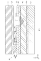
- FIG. 5 is an enlarged cross-sectional view of a main part schematically showing the configuration of the joint portion 60 shown in FIG. 4 and its surroundings.
- FIG. 5 is a cross section of a ZY plane in which the position of the X coordinate is different from the cross section shown in FIG.
- the Si substrate F2 is degenerate silicon (Si), and the Si substrate F2 itself also serves as a lower electrode of the resonator 10. Therefore, the above-mentioned metal layer E1 is not included.
- the joint portion 60 includes a eutectic layer 65 containing a eutectic alloy as a main component.
- the eutectic alloy of the eutectic layer 65 is, for example, a eutectic alloy of a first metal layer 61 containing aluminum (Al) as a main component and a second metal layer 62 of germanium (Ge).
- the first metal layer 61 and the second metal layer 62 are described as independent layers, but in reality, these interfaces are eutectic bonded. That is, the eutectic layer 65 is composed mainly of a eutectic alloy of a first metal containing aluminum (Al) as a main component and a second metal of germanium (Ge) as a main component. As described above, the joint portion 60 forms a eutectic alloy of the first metal of the first metal layer 61 containing aluminum (Al) as a main component and the second metal of the second metal layer 62 which is germanium (Ge). By including the eutectic layer 65 as a main component, it is possible to easily realize a bonded portion 60 having conductivity and high bonding strength.
- the first metal of the first metal layer 61 is composed of, for example, aluminum (Al), an aluminum-copper alloy (AlCu alloy), or an aluminum-silicon-copper alloy (AlSiCu alloy). Since aluminum or an aluminum alloy can be easily eutectic bonded to the germanium (Ge) of the second metal layer 62 and is a metal often used for wiring, for example, in a resonance device or the like, the manufacture of the resonance device 1 is performed. The process can be simplified, and the joint portion 60 for joining the MEMS substrate 50 and the upper lid 30 can be easily formed.
- the first metal of the first metal layer 61 is aluminum (Al)
- the second metal of the second metal layer 62 is germanium (Ge)
- the eutectic layer 65 is aluminum (Al)
- the eutectic layer 65 may contain aluminum (Al) and germanium (Ge) in addition to aluminum-germanium.
- a wiring layer 81 is provided on the parasitic capacitance reduction film 240 around the joint portion 60.
- the wiring layer 81 is configured to be electrically connected to the Si substrate F2 which has conductivity and functions as a lower electrode of the resonator 10.
- To form the wiring layer 81 first, a part of the parasitic capacitance reducing film 240 and the piezoelectric thin film F3 is removed, and holes are formed. Then, the hole is filled with a conductive material and electrically connected to the Si substrate F2.
- a diffusion prevention layer 85 is provided on the parasitic capacitance reduction film 240.
- the diffusion prevention layer 85 has conductivity and is configured to electrically connect the wiring layer 81 and the joint portion 60.
- the diffusion prevention layer 85 has a function of blocking and preventing the diffusion of the metal constituting the joint portion 60.
- the MEMS substrate 50 (resonant 10 and lower lid 20) includes the wiring layer 81 electrically connected to the Si substrate F2 which is the lower electrode of the resonator 10, so that the diffusion prevention layer 85 is interposed.
- the potential of the junction 60 can be reduced to the reference potential (GND) of the resonance device 1, and the generation of parasitic capacitance (stray capacitance) can be suppressed.
- the MEMS substrate 50 (resonator 10 and lower lid 20) includes the diffusion prevention layer 85 that electrically connects the wiring layer 81 and the bonding portion 60, the upper lid 30 and the MEMS substrate 50 are bonded.
- the diffusion prevention layer 85 can prevent the metal constituting the joint portion 60 from diffusing into the wiring layer 81. Therefore, it is possible to reduce the change in the metal ratio of the joint portion 60 due to diffusion, and it is possible to suppress the joint defect of the joint portion 60.
- the wiring layer 81 is formed at a position separated from the end portion of the joint portion 60.
- the wiring layer 81 is arranged on the MEMS substrate 50 (resonator 10 and lower lid 20) at a distance from the end portion of the joint portion 60. This makes it possible to arrange the diffusion prevention layer 85 between the joint portion 60 and the wiring layer 81. Therefore, the diffusion prevention layer 85 can be made thinner and the product cost of the resonance device 1 can be reduced as compared with the case where the diffusion prevention layer 85 is formed directly under the joint portion 60 described later.
- the material of the wiring layer 81 is preferably a metal containing aluminum (Al) as a main component.
- the metal containing aluminum (Al) as a main component is, for example, aluminum (Al), an aluminum-copper alloy (AlCu alloy), or an aluminum-silicon-copper alloy (AlSiCu alloy).
- the material of the wiring layer 81 is not limited to the case where it is a metal containing aluminum as a main component.
- the material of the wiring layer 81 may be a metal such as titanium (Ti).
- the wiring layer 81 is composed of a metal containing aluminum as a main component
- aluminum (Al) and silicon (Si) interact with each other at the interface between the wiring layer 81 and the Si substrate F2, as shown by the broken line in FIG. Diffuse, so-called alloy spikes, can occur.
- the silicon of the Si substrate F2 is in a state where it easily dissolves into the joint portion 60, and the role of the diffusion prevention layer 85 between the joint portion 60 and the joint portion 60 becomes even more important.
- the diffusion prevention layer 85 is composed of a metal having low diffusivity with respect to the metal of the joint portion 60.
- the material of the diffusion prevention layer 85 is preferably molybdenum (Mo) or tungsten (W), for example.
- Mo molybdenum
- W tungsten
- the material of the wiring layer 81 is aluminum (Al), and the material of the diffusion prevention layer 85 is molybdenum (Mo).
- FIG. 6 is a flowchart showing a manufacturing method of the resonance device 1 according to the embodiment.
- FIG. 7 is a cross-sectional view for explaining the process S301 shown in FIG.
- FIG. 8 is an enlarged cross-sectional view of a main part for explaining the first example of the step S302 shown in FIG.
- FIG. 9 is an enlarged cross-sectional view of a main part for explaining a second example of the step S302 shown in FIG.
- FIG. 10 is an enlarged cross-sectional view of a main part for explaining a third example of the step S302 shown in FIG. FIG.
- FIG. 11 is an enlarged cross-sectional view of a main part for explaining a fourth example of the step S302 shown in FIG.
- FIG. 12 is an enlarged cross-sectional view of a main part for explaining the process S303 shown in FIG.
- FIG. 13 is an enlarged cross-sectional view of a main part for explaining the step S304 shown in FIG. Note that FIGS. 7 to 13 show and describe one of the plurality of resonance devices 1 manufactured by the manufacturing method for convenience.
- the MEMS substrate 50 and the upper lid 30 are prepared (S301). Specifically, as shown in FIG. 7, the MEMS substrate 50 including the resonator 10 and the upper lid 30 described above are prepared. However, the connection wiring 70 shown in FIG. 4 for connecting the through electrode V3 and the resonator 10 has not yet been formed. Similarly, the joint portion 60, the wiring layer 81, and the diffusion prevention layer 85 shown in FIG. 5 have not yet been formed.
- the present invention is not limited to this.
- the MEMS substrate 50 and the upper lid 30 may be prepared separately for the process of preparing the MEMS substrate 50 and the process of preparing the upper lid 30.
- the first metal layer 61, the wiring layer 81, and the diffusion prevention layer 85 are formed on the MEMS substrate 50 prepared in the step S301 (S302).
- the parasitic capacitance reducing film 240 and the piezoelectric thin film F3 at predetermined positions are removed by etching or the like to form holes.
- the wiring layer 81 is formed by filling the holes formed with aluminum (Al) so as to be electrically connected to the Si substrate F2.
- molybdenum (Mo) is laminated on the ends of the parasitic capacitance reducing film 240 and the wiring layer 81, and the laminated molybdenum (Mo) is formed into a desired shape by etching or the like to form the laminated molybdenum (Mo) into a desired shape, thereby forming the diffusion prevention layer 85.
- the MEMS substrate 50 may be heat-treated for degassing at a high temperature, for example, about 435 ° C.
- the first metal layer 61 containing aluminum (Al) as a main component is less affected by heat diffusion even if it is heat-treated at a high temperature.
- FIG. 8 shows an example in which the first metal layer 61, the wiring layer 81, and the diffusion prevention layer 85 are formed on the MEMS substrate 50 in the order of the wiring layer 81, the diffusion prevention layer 85, and the first metal layer 61.
- Mo molybdenum
- a hole is formed at a predetermined position of the parasitic capacitance reducing film 240 to fill the hole with aluminum (Al), and aluminum (Al) is laminated on the ends of the parasitic capacitance reducing film 240 and the diffusion prevention layer 85.
- Al aluminum
- a hole is formed at a predetermined position of the parasitic capacitance reducing film 240, and the hole is filled with aluminum (Al).
- aluminum (Al) is laminated on the parasitic capacitance reducing film 240 to form the wiring layer 81 and the first metal layer 61, and then the parasitic capacitance reducing film 240, the end portion of the wiring layer 81, and Molybdenum (Mo) may be laminated on the end portion of the first metal layer 61 to form the anti-diffusion layer 85.
- the first metal layer 61 and the wiring layer 81 are formed on the upper layer or the lower layer of the diffusion prevention layer 85. can do. Therefore, the process of forming the first metal layer 61 and the wiring layer 81 can be reduced, and the manufacturing cost can be reduced.
- the diffusion prevention layer 85 may be composed of two or more layers.
- molybdenum (Mo) is laminated on the piezoelectric thin film F3 to form a metal layer E1 having a function as an upper electrode of the resonator 10 and a first layer 85a of the diffusion prevention layer 85.
- the parasitic capacitance reducing film 240 is laminated on the piezoelectric thin film F3 so as to cover the metal layer E1, and the protective film 235 is laminated at a predetermined position of the parasitic capacitance reducing film 240.
- molybdenum (Mo) is laminated on the first layer 85a at a predetermined position of the protective film 235 to form the frequency adjusting film 236 and the second layer 85b of the diffusion prevention layer 85. Then, a hole is formed at a predetermined position of the parasitic capacitance reducing film 240 to fill the hole with aluminum (Al), and aluminum (Al) is placed on the ends of the parasitic capacitance reducing film 240 and the diffusion prevention layer 85. By laminating, the wiring layer 81 and the first metal layer 61 are formed.
- the diffusion prevention layer 85 can be made thicker. It is possible to improve the blocking property that blocks the diffusion of the metal constituting the joint portion 60.
- the process S302 is not limited to the case where the process S302 is performed separately from the process S301.
- the formation of the first metal layer 61, the wiring layer 81, and the diffusion prevention layer 85 may be performed as a part of the step S301, or a part of the step of preparing the MEMS substrate 50 separated from the step S301. You may go as.
- the second metal layer 62 is formed on the upper lid 30 prepared in the step S301 (S303).
- germanium (Ge) is laminated on the surface of the silicon oxide film L31 on the back surface of the upper lid 30 to form the second metal layer 62 at a predetermined position.
- the predetermined position where the second metal layer 62 is formed is, for example, when the front surface of the MEMS substrate 50 and the back surface of the upper lid 30 face each other, the first metal formed on the MEMS substrate 50 on the back surface of the upper lid 30. It is a position facing or substantially facing the layer 61.
- the upper lid 30 is heat-treated for degassing at a high temperature, for example, about 435 ° C. As a result, the gas contained in the upper lid 30 and the second metal layer 62 can be sufficiently released (evaporated), and the generation of outgas can be reduced.
- the process S303 is not limited to the case where the process S303 is performed separately from the process S301.
- the formation of the second metal layer 62 may be performed as a part of the step S301, or may be performed as a part of the step of preparing the upper lid 30 separated from the step S301.
- a joint portion 60 including a eutectic layer 65 containing a eutectic alloy of a first metal containing aluminum (Al) as a main component and a second metal of germanium (Ge) as a main component is formed.
- the MEMS substrate 50 and the upper lid 30 are aligned so that the first metal layer 61 and the second metal layer 62 coincide with each other.
- the MEMS substrate 50 and the upper lid 30 are sandwiched by a heater or the like, and heat treatment for the eutectic reaction is performed.
- the upper lid 30 is moved toward the MEMS substrate 50.
- the second metal layer 62 comes into contact with the first metal layer 61.
- the temperature in the heat treatment for eutectic bonding is preferably the temperature of the confocal or higher and lower than the melting point of aluminum (Al) alone, that is, about 424 ° C or higher and lower than 620 ° C.
- the heating time is preferably about 10 minutes or more and 20 minutes or less.
- the heat treatment is performed at a temperature of 430 ° C. or higher and 500 ° C. or lower for about 15 minutes.
- the upper lid 30 and the MEMS substrate 50 are pressed from the upper lid 30 to the MEMS substrate 50 as shown by the black arrow in FIG.
- the pressure to be pressed is preferably about 5 MPa or more and 25 MPa or less.
- a cooling treatment is performed, for example, by natural cooling.
- the cooling treatment is not limited to natural cooling, as long as the eutectic layer 65 can be formed at the joint portion 60, and the cooling temperature and cooling speed thereof can be variously selected.
- a joint portion 60 including a eutectic layer 65 containing a eutectic alloy of a first metal and a second metal as a main component is formed.
- connection wiring 70 shown in FIG. 4 for connecting the through electrode V3 and the resonator 10 may be provided.
- the wiring layer 81 is arranged at a distance from the end portion of the joint portion 60 in the MEMS substrate 50, but the present invention is not limited to this.
- the position where the wiring layer 81 is formed and arranged can be appropriately changed.
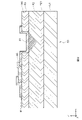
- FIG. 14 is an enlarged cross-sectional view of a main part schematically showing a modified example of the configuration of the joint portion 60 and its surroundings shown in FIG.
- the same configurations as those of the joint portion 60 shown in FIG. 5 are designated by the same reference numerals, and the description thereof will be omitted as appropriate.
- similar actions and effects with the same configuration will not be mentioned sequentially.
- the wiring layer 81A and the diffusion prevention layer 85A may be provided under the joint portion 60, respectively.
- the wiring layer 81A is formed in a part around the vibrating portion 120 in the resonator 10.
- a diffusion prevention layer 85A is formed on the wiring layer 81A so as to cover the wiring layer 81A.
- the first metal layer 61 is formed on the diffusion prevention layer 85A.
- the eutectic layer 65 is formed by eutectic bonding the first metal layer 61 on the diffusion prevention layer 85A formed on the MEMS substrate 50 and the second metal layer 62 formed on the back surface of the upper lid 30 in this way.
- the including joint 60 is formed.
- the MEMS substrate comprises a wiring layer that is electrically connected to the lower electrode of the resonator.
- the potential of the junction can be reduced to the reference potential (GND) of the resonance device via the diffusion prevention layer, and the generation of parasitic capacitance (stray capacitance) can be suppressed.
- the MEMS substrate includes a diffusion prevention layer that electrically connects the wiring layer and the joint portion.
- the joint portion is a eutectic alloy of the first metal of the first metal layer containing aluminum (Al) as a main component and the second metal of the second metal layer which is germanium (Ge). Includes a eutectic layer whose main component is. As a result, it is possible to easily realize a joint portion having conductivity and high joint strength.
- the material of the diffusion prevention layer is molybdenum (Mo) or tungsten (W).
- the material of the Si substrate is degenerate silicon (Si).
- Si degenerate silicon
- the Si substrate itself can also serve as a lower electrode of the resonator.
- the material of the wiring layer is a metal containing aluminum (Al) as a main component. This makes it possible to remove (reduce) the oxide film formed on the surface of the Si substrate, which is the lower electrode of the resonator, by heat treatment at a relatively low temperature, for example, 450 ° C.
- the wiring layer is arranged on the MEMS substrate at a distance from the end portion of the joint portion. This makes it possible to arrange a diffusion prevention layer between the joint portion and the wiring layer. Therefore, as compared with the case where the diffusion prevention layer is formed directly under the joint portion, the diffusion prevention layer can be made thinner, and the product cost of the resonance device can be reduced.
- the first metal layer, the resonator, the wiring layer electrically connected to the Si substrate which is the lower electrode of the resonator, the wiring layer, and the first metal layer includes a step of preparing a MEMS substrate comprising an anti-diffusion layer for electrically connecting the two.
- the potential of the junction can be reduced to the reference potential (GND) of the resonance device via the diffusion prevention layer, and the generation of parasitic capacitance (stray capacitance) can be suppressed.
- the MEMS substrate includes a diffusion prevention layer that electrically connects the wiring layer and the joint portion.
- the metal constituting the joined portion can be prevented from diffusing into the wiring layer by the diffusion prevention layer. Therefore, it is possible to reduce the change in the metal ratio of the joint portion due to diffusion, and it is possible to suppress the joint failure of the joint portion.
- the step of preparing the MEMS substrate includes forming the first metal layer and the wiring layer before or after the formation of the diffusion prevention layer.
- the first metal layer and the wiring layer can be formed on the upper layer or the lower layer of the diffusion prevention layer. Therefore, the process of forming the first metal layer and the wiring layer can be reduced, and the manufacturing cost can be reduced.
- the steps of preparing the MEMS substrate include forming the first layer of the diffusion prevention layer, forming the second layer of the diffusion prevention layer on the first layer, and forming the second layer of the diffusion prevention layer. including.
- the diffusion prevention layer can be made thicker, and the blocking property for blocking the diffusion of the metal constituting the joint can be improved.
- the step of preparing a MEMS substrate includes forming a wiring layer at a position at a distance from the end of the joint portion in the MEMS substrate. This makes it possible to arrange a diffusion prevention layer between the joint portion and the wiring layer. Therefore, as compared with the case where the diffusion prevention layer is formed directly under the joint portion, the diffusion prevention layer can be made thinner, and the product cost of the resonance device can be reduced.
- the first metal of the first metal layer is a metal containing aluminum (Al) as a main component
- the second metal of the second metal layer is germanium (Ge).
- the material of the diffusion prevention layer is molybdenum (Mo) or tungsten (W).
- the material of the Si substrate is degenerate silicon (Si).
- Si degenerate silicon
- the Si substrate itself can also serve as a lower electrode of the resonator.
- the material of the wiring layer is a metal containing aluminum (Al) as a main component. This makes it possible to remove (reduce) the oxide film formed on the surface of the Si substrate, which is the lower electrode of the resonator, by heat treatment at a relatively low temperature, for example, 450 ° C.
- Base 131a ... Long side, 131A ... Front end, 131b ... Long side, 131B ... Rear end, 131c ... short side, 131d ... short side, 135, 135A, 135B, 135C, 135D ... vibrating arm, 140 holding part, 141 ... voltage application part, 235 ... protective film, 236 ... frequency adjustment film, 240 ... parasitic capacity reduction film, E1 ... metal layer, E2 ... metal layer, F2 ... Si substrate, F3 ... piezoelectric thin film, F21 ... silicon oxide layer, G ... weight part, L1 ... Si wafer, L3 ... Si substrate, L31 ... silicon oxide film, P ... virtual Flat surface, T4 ... terminal, V1 ... via, V2 ... via, V3 ... through electrode.
Abstract
Provided are a resonance device and a resonance device manufacturing method that make it possible to suppress junction defects at a junction. The resonance device 1 comprises: a MEMS substrate 50 that includes a resonator 10; a top cover 30; and a junction 60 that is electroconductive and that joins the MEMS substrate 50 and the top cover 30. The MEMS substrate 50 further includes: a wiring layer 81 that is electrically connected to a Si substrate F2, which is a lower electrode of the resonator 10; and a diffusion prevention layer 85 that electrically connects the wiring layer 81 and the junction 60.
Description
本発明は、共振装置及び共振装置製造方法に関する。
The present invention relates to a resonance device and a method for manufacturing a resonance device.
従来、MEMS(Micro Electro Mechanical Systems)技術を用いて製造された共振装置が普及している。このデバイスは、例えば共振子を有する下側基板に、上側基板を接合して形成される。
Conventionally, a resonance device manufactured by using MEMS (Micro Electro Mechanical Systems) technology has become widespread. This device is formed by joining an upper substrate to, for example, a lower substrate having a resonator.
例えば、特許文献1には、共振子を有する下側基板と、素子と対向して設けられた上側基板と、素子の周囲において、下側基板と上側基板とを接合する接合部と、を備え、接合部は、過共晶合金を含む領域と、共晶合金を含む領域とを有するMEMSデバイスが開示されている。このMEMSデバイスは、過共晶合金が共晶合金を覆うことで、共晶接合の接合面から金属がはみ出ることを防いでいる。
For example, Patent Document 1 includes a lower substrate having a resonator, an upper substrate provided facing the element, and a joint portion for joining the lower substrate and the upper substrate around the element. , A MEMS device having a region containing a hypereutectic alloy and a region containing a eutectic alloy is disclosed as a junction. In this MEMS device, the hypereutectic alloy covers the eutectic alloy to prevent the metal from squeezing out from the joint surface of the eutectic joint.
ところで、接合部をグランド(GND)に接続して寄生容量(浮遊容量)の発生を抑制することで、MEMSデバイスの特性の向上を図ることがある。この場合、接合部と共振子の下部電極とは、良好な電気接続性を有するアルミニウム(Al)の配線で接続されていた。
By the way, the characteristics of the MEMS device may be improved by connecting the joint portion to the ground (GND) to suppress the generation of parasitic capacitance (stray capacitance). In this case, the joint and the lower electrode of the resonator were connected by an aluminum (Al) wiring having good electrical connectivity.
しかしながら、接合の際に、接合部を構成する金属、例えばゲルマニウム(Ge)がアルミニウムの配線に拡散し、共振子の下部電極側に流れ込むおそれがあった。そのため、接合部を構成する金属の比率が変化してしまい、共晶比率(共晶比)が変化したり、共晶反応が不十分になったりすることがあった。その結果、接合部の接合強度が低下する等の接合不良が発生する場合があった。
However, at the time of joining, there is a possibility that the metal constituting the joining portion, for example, germanium (Ge), diffuses into the aluminum wiring and flows into the lower electrode side of the resonator. Therefore, the ratio of the metals constituting the joint portion may change, the eutectic ratio (eutectic ratio) may change, or the eutectic reaction may become insufficient. As a result, there are cases where joint defects such as a decrease in the joint strength of the joint portion occur.
本発明はこのような事情に鑑みてなされたものであり、接合部の接合不良を抑制することのできる共振装置及び共振装置製造方法を提供することを目的の1つとする。
The present invention has been made in view of such circumstances, and one of the objects of the present invention is to provide a resonance device and a method for manufacturing a resonance device capable of suppressing joint defects in a joint portion.
本発明の一側面に係る共振装置は、共振子を含む第1基板と、第2基板と、導電性を有し、第1基板と第2基板とを接合する接合部と、を備え、第1基板は、共振子の下部電極と電気的に接続される配線層と、該配線層と接合部とを電気的に接続する拡散防止層と、をさらに含む。
The resonance device according to one aspect of the present invention includes a first substrate including a resonator, a second substrate, and a joint portion having conductivity and joining the first substrate and the second substrate. One substrate further includes a wiring layer that is electrically connected to the lower electrode of the resonator and a diffusion prevention layer that electrically connects the wiring layer and the joint portion.
本発明の他の一側面に係る共振装置製造方法は、第1金属層と、共振子と、該共振子の下部電極と電気的に接続される配線層と、該配線層と第1金属層とを電気的に接続する拡散防止層と、を含む第1基板を用意する工程と、第2金属層を含む第2基板を用意する工程と、第1基板と第2基板とを接合する工程であって、第1金属層の第1金属と第2金属層の第2金属との共晶合金を主成分とする共晶層を含む接合部を形成する、接合する工程と、を含む。
A method for manufacturing a resonator according to another aspect of the present invention includes a first metal layer, a resonator, a wiring layer electrically connected to a lower electrode of the resonator, and the wiring layer and the first metal layer. A step of preparing a first substrate including a diffusion prevention layer for electrically connecting the above, a step of preparing a second substrate including a second metal layer, and a step of joining the first substrate and the second substrate. It includes a step of forming a joint portion including a eutectic layer containing a eutectic alloy of the first metal of the first metal layer and the second metal of the second metal layer as a main component, and joining.
本発明によれば、接合部の接合不良を抑制することができる。
According to the present invention, it is possible to suppress joint defects in the joint portion.
以下に本発明の実施形態を説明する。以下の図面の記載において、同一又は類似の構成要素は同一又は類似の符号で表している。図面は例示であり、各部の寸法や形状は模式的なものであり、本発明の技術的範囲を当該実施形態に限定して解するべきではない。
An embodiment of the present invention will be described below. In the description of the drawings below, the same or similar components are represented by the same or similar reference numerals. The drawings are examples, and the dimensions and shapes of each part are schematic, and the technical scope of the present invention should not be limited to the embodiment.
<実施形態>
まず、図1及び図2を参照しつつ、本発明の一実施形態に従う共振装置の概略構成について説明する。図1は、一実施形態における共振装置1の外観を概略的に示す斜視図である。図2は、図1に示した共振装置1の構造を概略的に示す分解斜視図である。 <Embodiment>
First, a schematic configuration of a resonance device according to an embodiment of the present invention will be described with reference to FIGS. 1 and 2. FIG. 1 is a perspective view schematically showing the appearance of theresonance device 1 in one embodiment. FIG. 2 is an exploded perspective view schematically showing the structure of the resonance device 1 shown in FIG.
まず、図1及び図2を参照しつつ、本発明の一実施形態に従う共振装置の概略構成について説明する。図1は、一実施形態における共振装置1の外観を概略的に示す斜視図である。図2は、図1に示した共振装置1の構造を概略的に示す分解斜視図である。 <Embodiment>
First, a schematic configuration of a resonance device according to an embodiment of the present invention will be described with reference to FIGS. 1 and 2. FIG. 1 is a perspective view schematically showing the appearance of the
共振装置1は、下蓋20と、共振子10(以下、下蓋20と共振子10とを合わせて「MEMS基板50」ともいう。)と、上蓋30と、を備えている。すなわち、共振装置1は、MEMS基板50と、接合部60と、上蓋30とが、この順で積層されて構成されている。なお、MEMS基板50は本発明の「第1基板」の一例に相当し、上蓋30は本発明の「第2基板」の一例に相当する。
The resonator 1 includes a lower lid 20, a resonator 10 (hereinafter, the lower lid 20 and the resonator 10 are collectively referred to as a “MEMS substrate 50”), and an upper lid 30. That is, the resonator 1 is configured by laminating the MEMS substrate 50, the joint portion 60, and the upper lid 30 in this order. The MEMS substrate 50 corresponds to an example of the "first substrate" of the present invention, and the upper lid 30 corresponds to an example of the "second substrate" of the present invention.
以下において、共振装置1の各構成について説明する。なお、以下の説明では、共振装置1のうち上蓋30が設けられている側を上(又は表)、下蓋20が設けられている側を下(又は裏)、として説明する。
Hereinafter, each configuration of the resonance device 1 will be described. In the following description, the side of the resonance device 1 where the upper lid 30 is provided is referred to as the upper side (or the front side), and the side where the lower lid 20 is provided is referred to as the lower side (or the back side).
共振子10は、MEMS技術を用いて製造されるMEMS振動子である。共振子10と上蓋30とは、後述する接合部60を介して接合されている。また、共振子10と下蓋20は、それぞれシリコン(Si)基板(以下、「Si基板」という)を用いて形成されており、Si基板同士が互いに接合されている。なお、MEMS基板50(共振子10及び下蓋20)は、SOI基板を用いて形成されてもよい。
The resonator 10 is a MEMS oscillator manufactured using MEMS technology. The resonator 10 and the upper lid 30 are joined via a joint portion 60, which will be described later. Further, the resonator 10 and the lower lid 20 are each formed of a silicon (Si) substrate (hereinafter referred to as “Si substrate”), and the Si substrates are bonded to each other. The MEMS substrate 50 (resonator 10 and lower lid 20) may be formed by using an SOI substrate.
上蓋30はXY平面に沿って平板状に広がっており、その裏面に例えば平たい直方体形状の凹部31が形成されている。凹部31は、側壁33に囲まれており、共振子10が振動する空間である振動空間の一部を形成する。また、上蓋30の凹部31の共振子10側の面には、後述するゲッター層34が形成されている。なお、上蓋30は凹部31を有さず、平板状の構成でもよい。
The upper lid 30 extends in a flat plate shape along the XY plane, and for example, a flat rectangular parallelepiped concave portion 31 is formed on the back surface thereof. The recess 31 is surrounded by the side wall 33 and forms a part of the vibration space, which is the space where the resonator 10 vibrates. Further, a getter layer 34, which will be described later, is formed on the surface of the concave portion 31 of the upper lid 30 on the resonator 10 side. The upper lid 30 does not have a recess 31, and may have a flat plate shape.
下蓋20は、XY平面に沿って設けられる矩形平板状の底板22と、底板22の周縁部からZ軸方向、つまり、下蓋20と共振子10との積層方向、に延びる側壁23と、を有する。下蓋20には、共振子10と対向する面において、底板22の表面と側壁23の内面とによって形成される凹部21が形成されている。凹部21は、共振子10の振動空間の一部を形成する。なお、下蓋20は凹部21を有さず、平板状の構成でもよい。また、下蓋20の凹部21の共振子10側の面には、ゲッター層が形成されてもよい。
The lower lid 20 includes a rectangular flat plate-shaped bottom plate 22 provided along the XY plane, and a side wall 23 extending in the Z-axis direction from the peripheral edge of the bottom plate 22, that is, in the stacking direction of the lower lid 20 and the resonator 10. Has. The lower lid 20 is formed with a recess 21 formed by the surface of the bottom plate 22 and the inner surface of the side wall 23 on the surface facing the resonator 10. The recess 21 forms a part of the vibration space of the resonator 10. The lower lid 20 does not have the recess 21 and may have a flat plate shape. Further, a getter layer may be formed on the surface of the lower lid 20 on the resonator 10 side of the recess 21.
次に、図3を参照しつつ、本発明の一実施形態に従う共振装置に含まれる共振子の概略構成について説明する。図3は、図2に示した共振子10の構造を概略的に示す平面図である。
Next, with reference to FIG. 3, a schematic configuration of the resonator included in the resonator according to the embodiment of the present invention will be described. FIG. 3 is a plan view schematically showing the structure of the resonator 10 shown in FIG.
図3に示すように、共振子10は、MEMS技術を用いて製造されるMEMS振動子であり、図3の直交座標系におけるXY平面内で面外振動する。なお、共振子10は、面外屈曲振動モードを用いた共振子に限定されるものではない。共振装置1の共振子は、例えば、広がり振動モード、厚み縦振動モード、ラム波振動モード、面内屈曲振動モード、表面波振動モードを用いるものであってもよい。これらの振動子は、例えば、タイミングデバイス、RFフィルタ、デュプレクサ、超音波トランスデューサー、ジャイロセンサ、加速度センサ等に応用される。また、アクチュエーター機能を持った圧電ミラー、圧電ジャイロ、圧力センサ機能を持った圧電マイクロフォン、超音波振動センサ等に用いられてもよい。さらに、静電MEMS素子、電磁駆動MEMS素子、ピエゾ抵抗MEMS素子に適用してもよい。
As shown in FIG. 3, the resonator 10 is a MEMS oscillator manufactured by using the MEMS technique, and vibrates out of the plane in the XY plane in the Cartesian coordinate system of FIG. The resonator 10 is not limited to the resonator using the out-of-plane bending vibration mode. The resonator of the resonator 1 may use, for example, a spread vibration mode, a thickness longitudinal vibration mode, a lamb wave vibration mode, an in-plane bending vibration mode, and a surface wave vibration mode. These oscillators are applied to, for example, timing devices, RF filters, duplexers, ultrasonic transducers, gyro sensors, acceleration sensors and the like. Further, it may be used for a piezoelectric mirror having an actuator function, a piezoelectric gyro, a piezoelectric microphone having a pressure sensor function, an ultrasonic vibration sensor, or the like. Further, it may be applied to an electrostatic MEMS element, an electromagnetically driven MEMS element, and a piezo resistance MEMS element.
共振子10は、振動部120と、保持部140と、保持腕110と、を備える。
The resonator 10 includes a vibrating portion 120, a holding portion 140, and a holding arm 110.
保持部140は、XY平面に沿って振動部120の外側を囲むように、矩形の枠状に形成される。例えば、保持部140は、角柱形状の枠体から一体に形成されている。なお、保持部140は、振動部120の周囲の少なくとも一部に設けられていればよく、枠状の形状に限定されるものではない。
The holding portion 140 is formed in a rectangular frame shape so as to surround the outside of the vibrating portion 120 along the XY plane. For example, the holding portion 140 is integrally formed from a prismatic frame. The holding portion 140 may be provided at least in at least a part around the vibrating portion 120, and is not limited to the frame shape.
保持腕110は、保持部140の内側に設けられ、振動部120と保持部140とを接続する。
The holding arm 110 is provided inside the holding portion 140, and connects the vibrating portion 120 and the holding portion 140.
振動部120は、保持部140の内側に設けられており、振動部120と保持部140との間には、所定の間隔で空間が形成されている。図3に示す例では、振動部120は、基部130と4本の振動腕135A~135D(以下、まとめて「振動腕135」ともいう)と、を有している。なお、振動腕の数は、4本に限定されるものではなく、例えば1本以上の任意の数に設定される。本実施形態において、各振動腕135A~135Dと、基部130とは、一体に形成されている。
The vibrating portion 120 is provided inside the holding portion 140, and a space is formed between the vibrating portion 120 and the holding portion 140 at a predetermined interval. In the example shown in FIG. 3, the vibrating portion 120 has a base 130 and four vibrating arms 135A to 135D (hereinafter, collectively referred to as “vibrating arm 135”). The number of vibrating arms is not limited to four, but is set to, for example, an arbitrary number of one or more. In the present embodiment, the vibrating arms 135A to 135D and the base 130 are integrally formed.
基部130は、平面視において、X軸方向に長辺131a、131b、Y軸方向に短辺131c、131dを有している。長辺131aは、基部130の前端の面(以下、「前端131A」ともいう)の一つの辺であり、長辺131bは基部130の後端の面(以下、「後端131B」ともいう)の一つの辺である。基部130において、前端131Aと後端131Bとは、互いに対向するように設けられている。
The base 130 has long sides 131a and 131b in the X-axis direction and short sides 131c and 131d in the Y-axis direction in a plan view. The long side 131a is one side of the front end surface of the base 130 (hereinafter, also referred to as “front end 131A”), and the long side 131b is the rear end surface of the base 130 (hereinafter, also referred to as “rear end 131B”). It is one side of. In the base 130, the front end 131A and the rear end 131B are provided so as to face each other.
基部130は、前端131Aにおいて、振動腕135に接続され、後端131Bにおいて、後述する保持腕110に接続されている。なお、基部130は、図3に示す例では平面視において、略長方形の形状を有しているがこれに限定されるものではない。基部130は、長辺131aの垂直二等分線に沿って規定される仮想平面Pに対して略面対称に形成されていればよい。例えば、基部130は、長辺131bが131aより短い台形であってもよいし、長辺131aを直径とする半円の形状であってもよい。また、基部130の各面は平面に限定されるものではなく、湾曲した面であってもよい。なお、仮想平面Pは、振動部120における、振動腕135が並ぶ方向の中心を通る平面である。
The base 130 is connected to the vibrating arm 135 at the front end 131A and is connected to the holding arm 110 described later at the rear end 131B. In the example shown in FIG. 3, the base 130 has a substantially rectangular shape in a plan view, but the base 130 is not limited thereto. The base 130 may be formed substantially symmetrically with respect to the virtual plane P defined along the perpendicular bisector of the long side 131a. For example, the base 130 may have a trapezoidal shape in which the long side 131b is shorter than 131a, or may have a semicircular shape having the long side 131a as a diameter. Further, each surface of the base 130 is not limited to a flat surface, and may be a curved surface. The virtual plane P is a plane that passes through the center of the vibrating portion 120 in the direction in which the vibrating arms 135 are lined up.
基部130において、前端131Aから後端131Bに向かう方向における、前端131Aと後端131Bとの最長距離である基部長は35μm程度である。また、基部長方向に直交する幅方向であって、基部130の側端同士の最長距離である基部幅は265μm程度である。
In the base 130, the base length, which is the longest distance between the front end 131A and the rear end 131B in the direction from the front end 131A to the rear end 131B, is about 35 μm. Further, the base width, which is the width direction orthogonal to the base length direction and is the longest distance between the side ends of the base 130, is about 265 μm.
振動腕135は、Y軸方向に延び、それぞれ同一のサイズを有している。振動腕135は、それぞれが基部130と保持部140との間にY軸方向に平行に設けられ、一端は、基部130の前端131Aと接続されて固定端となっており、他端は開放端となっている。また、振動腕135は、それぞれ、X軸方向に所定の間隔で、並列して設けられている。なお、振動腕135は、例えばX軸方向の幅が50μm程度、Y軸方向の長さが465μm程度である。
The vibrating arm 135 extends in the Y-axis direction and has the same size. Each of the vibrating arms 135 is provided between the base 130 and the holding portion 140 in parallel in the Y-axis direction, one end is connected to the front end 131A of the base 130 to be a fixed end, and the other end is an open end. It has become. Further, the vibrating arms 135 are provided in parallel at predetermined intervals in the X-axis direction, respectively. The vibrating arm 135 has, for example, a width of about 50 μm in the X-axis direction and a length of about 465 μm in the Y-axis direction.
振動腕135は、それぞれ、例えば開放端から150μm程度の部分が、振動腕135の他の部位よりもX軸方向の幅が広くなっている。この幅が広くなった部位は、錘部Gと呼ばれる。錘部Gは、例えば、振動腕135の他の部位よりも、X軸方向に沿って左右に幅が10μmずつ広く、X軸方向の幅が70μm程度である。錘部Gは、振動腕135と同一プロセスによって一体形成される。錘部Gが形成されることで、振動腕135は、単位長さ当たりの重さが、固定端側よりも開放端側の方が重くなっている。従って、振動腕135のそれぞれが開放端側に錘部Gを有することで、各振動腕における上下方向の振動の振幅を大きくすることができる。
Each of the vibrating arms 135 has a wider width in the X-axis direction than other parts of the vibrating arm 135, for example, at a portion about 150 μm from the open end. The portion where this width is widened is called a weight portion G. The weight portion G has a width of 10 μm to the left and right along the X-axis direction and a width of about 70 μm in the X-axis direction, for example, as compared with other parts of the vibrating arm 135. The weight portion G is integrally formed by the same process as the vibrating arm 135. By forming the weight portion G, the vibrating arm 135 has a heavier weight per unit length on the open end side than on the fixed end side. Therefore, since each of the vibrating arms 135 has the weight portion G on the open end side, the amplitude of the vertical vibration in each vibrating arm can be increased.
振動部120の表面(上蓋30に対向する面)には、その全面を覆うように後述の保護膜235が形成されている。また、振動腕135A~135Dの開放端側の先端における保護膜235の表面には、それぞれ、周波数調整膜236が形成されている。保護膜235及び周波数調整膜236によって、振動部120の共振周波数を調整することができる。
A protective film 235, which will be described later, is formed on the surface of the vibrating portion 120 (the surface facing the upper lid 30) so as to cover the entire surface thereof. Further, a frequency adjusting film 236 is formed on the surface of the protective film 235 at the tip on the open end side of the vibrating arms 135A to 135D, respectively. The resonance frequency of the vibrating unit 120 can be adjusted by the protective film 235 and the frequency adjusting film 236.
なお、本実施形態では、共振子10の表面(上蓋30と対向する側の面)は、その略全面が保護膜235によって覆われている。さらに保護膜235の表面は、その略全面が寄生容量低減膜240で覆われている。ただし、保護膜235は少なくとも振動腕135を覆っていればよく、共振子10の略全面を覆う構成に限定されるものではない。
In the present embodiment, the surface of the resonator 10 (the surface on the side facing the upper lid 30) is almost entirely covered with the protective film 235. Further, the surface of the protective film 235 is almost entirely covered with the parasitic capacitance reducing film 240. However, the protective film 235 only needs to cover at least the vibrating arm 135, and is not limited to a configuration that covers substantially the entire surface of the resonator 10.
次に、図4を参照しつつ、本発明の一実施形態に従う共振装置1の積層構造について説明する。図4は、図1から図3に示した共振装置1のIV-IV線に沿った断面の構成を概略的に示す断面図である。
Next, with reference to FIG. 4, the laminated structure of the resonance device 1 according to the embodiment of the present invention will be described. FIG. 4 is a cross-sectional view schematically showing the configuration of a cross section of the resonance device 1 shown in FIGS. 1 to 3 along the IV-IV line.
図4に示すように、共振装置1は、下蓋20の側壁23上に共振子10の保持部140が接合され、さらに共振子10の保持部140と上蓋30の側壁33とが接合される。このように下蓋20と上蓋30との間に共振子10が保持され、下蓋20と上蓋30と共振子10の保持部140とによって、振動腕135が振動する振動空間が形成される。また、上蓋30の上面(共振子10と対向する面と反対側の面)には端子T4が形成されている。端子T4と共振子10とは、貫通電極V3、接続配線70、及びコンタクト電極76A,76Bによって電気的に接続されている。
As shown in FIG. 4, in the resonator 1, the holding portion 140 of the resonator 10 is joined on the side wall 23 of the lower lid 20, and the holding portion 140 of the resonator 10 and the side wall 33 of the upper lid 30 are further joined. .. In this way, the resonator 10 is held between the lower lid 20 and the upper lid 30, and the lower lid 20, the upper lid 30, and the holding portion 140 of the resonator 10 form a vibration space in which the vibrating arm 135 vibrates. Further, a terminal T4 is formed on the upper surface of the upper lid 30 (the surface opposite to the surface facing the resonator 10). The terminal T4 and the resonator 10 are electrically connected by a through electrode V3, a connection wiring 70, and contact electrodes 76A and 76B.
上蓋30は、所定の厚みを有するSi基板L3により形成されている。上蓋30はその周辺部(側壁33)で後述する接合部60によって共振子10の保持部140と接合されている。上蓋30における、共振子10に対向する表面は、酸化ケイ素膜L31に覆われている。酸化ケイ素膜L31は、例えば二酸化シリコン(SiO2)であり、Si基板L3の表面の酸化や、化学気相蒸着(CVD:Chemical Vapor Deposition)によって、Si基板L3の表面に形成される。なお、上蓋30の裏面及び貫通電極V3の側面についても、酸化ケイ素膜L31に覆われていることが好ましい。
The upper lid 30 is formed of a Si substrate L3 having a predetermined thickness. The upper lid 30 is joined to the holding portion 140 of the resonator 10 by a joining portion 60 described later at a peripheral portion (side wall 33) thereof. The surface of the upper lid 30 facing the resonator 10 is covered with the silicon oxide film L31. The silicon oxide film L31 is, for example, silicon dioxide (SiO 2 ), and is formed on the surface of the Si substrate L3 by oxidation of the surface of the Si substrate L3 or chemical vapor deposition (CVD). It is preferable that the back surface of the upper lid 30 and the side surface of the through silicon via V3 are also covered with the silicon oxide film L31.
また、上蓋30の凹部31における、共振子10と対向する側の面にはゲッター層34が形成されている。ゲッター層34は、例えばチタン(Ti)等から形成され、振動空間に発生するアウトガスを吸着する。本実施形態に係る上蓋30には、凹部31において共振子10に対向する面のほぼ全面にゲッター層34が形成されるため、振動空間の真空度の低下を抑制することができる。
Further, a getter layer 34 is formed on the surface of the recess 31 of the upper lid 30 on the side facing the resonator 10. The getter layer 34 is formed of, for example, titanium (Ti) or the like, and adsorbs outgas generated in the vibration space. In the upper lid 30 according to the present embodiment, since the getter layer 34 is formed on almost the entire surface of the concave portion 31 facing the resonator 10, it is possible to suppress a decrease in the degree of vacuum in the vibration space.
また、上蓋30の貫通電極V3は、上蓋30に形成された貫通孔に導電性材料が充填されて形成される。充填される導電性材料は、例えば、不純物ドープされた多結晶シリコン(Poly-Si)、銅(Cu)、金(Au)、不純物ドープされた単結晶シリコン等である。貫通電極V3は、端子T4と電圧印加部141とを電気的に接続させる配線としての役割を果たす。
Further, the through electrode V3 of the upper lid 30 is formed by filling the through holes formed in the upper lid 30 with a conductive material. The filled conductive material is, for example, impurity-doped polysilicon (Poly-Si), copper (Cu), gold (Au), impurity-doped single crystal silicon, or the like. The through electrode V3 serves as a wiring for electrically connecting the terminal T4 and the voltage application unit 141.
下蓋20の底板22及び側壁23は、SiウエハL1により、一体的に形成されている。また、下蓋20は、側壁23の上面によって、共振子10の保持部140と接合されている。Z軸方向に規定される下蓋20の厚みは例えば、150μm、凹部21の深さは例えば50μmである。なお、SiウエハL1は、縮退されていないシリコンから形成されており、その抵抗率は例えば16mΩ・cm以上である。
The bottom plate 22 and the side wall 23 of the lower lid 20 are integrally formed by the Si wafer L1. Further, the lower lid 20 is joined to the holding portion 140 of the resonator 10 by the upper surface of the side wall 23. The thickness of the lower lid 20 defined in the Z-axis direction is, for example, 150 μm, and the depth of the recess 21 is, for example, 50 μm. The Si wafer L1 is made of non-degenerate silicon, and its resistivity is, for example, 16 mΩ · cm or more.
共振子10における、保持部140、基部130、振動腕135、及び保持腕110は、同一プロセスで一体的に形成される。共振子10は、基板の一例であるSi基板F2の上に、Si基板F2を覆うように圧電薄膜F3が形成され、さらに圧電薄膜F3の上には、金属層E2が積層されている。そして、金属層E2の上には、金属層E2を覆うように圧電薄膜F3が積層されており、さらに、圧電薄膜F3の上には、金属層E1が積層されている。金属層E1の上には、金属層E1を覆うように保護膜235が積層され、保護膜235の上には寄生容量低減膜240が積層されている。保持部140、基部130、振動腕135、及び保持腕110のそれぞれの外形は、前述したSi基板F2、圧電薄膜F3、金属層E2、金属層E1、保護膜235等から構成される積層体を、例えばアルゴン(Ar)イオンビームを照射するドライエッチングによって除去加工し、パターニングすることによって形成される。
The holding portion 140, the base 130, the vibrating arm 135, and the holding arm 110 in the resonator 10 are integrally formed by the same process. In the resonator 10, a piezoelectric thin film F3 is formed on a Si substrate F2, which is an example of a substrate, so as to cover the Si substrate F2, and a metal layer E2 is laminated on the piezoelectric thin film F3. The piezoelectric thin film F3 is laminated on the metal layer E2 so as to cover the metal layer E2, and the metal layer E1 is further laminated on the piezoelectric thin film F3. A protective film 235 is laminated on the metal layer E1 so as to cover the metal layer E1, and a parasitic capacitance reducing film 240 is laminated on the protective film 235. The outer shape of each of the holding portion 140, the base portion 130, the vibrating arm 135, and the holding arm 110 is a laminate composed of the Si substrate F2, the piezoelectric thin film F3, the metal layer E2, the metal layer E1, the protective film 235, and the like described above. For example, it is formed by removing and patterning by dry etching which irradiates an argon (Ar) ion beam.
Si基板F2は、例えば、厚さ6μm程度の縮退したn型シリコン(Si)半導体から形成されていてもよい。縮退シリコン(Si)は、n型ドーパントとしてリン(P)やヒ素(As)、アンチモン(Sb)等を含むことができる。Si基板F2に用いられる縮退シリコン(Si)の抵抗値は、例えば16mΩ・cm未満であり、より好ましくは1.2mΩ・cm以下である。
The Si substrate F2 may be formed of, for example, a degenerate n-type silicon (Si) semiconductor having a thickness of about 6 μm. The degenerate silicon (Si) can contain phosphorus (P), arsenic (As), antimony (Sb) and the like as n-type dopants. The resistance value of the degenerate silicon (Si) used for the Si substrate F2 is, for example, less than 16 mΩ · cm, more preferably 1.2 mΩ · cm or less.
このように、Si基板F2が、縮退シリコン(Si)であることにより、例えば低抵抗値である縮退シリコン基板を用いることで、Si基板F2自体が共振子10の下部電極の役割を兼ねることができる。この場合、前述した金属層E2は省略される。
As described above, since the Si substrate F2 is degenerate silicon (Si), for example, by using a degenerate silicon substrate having a low resistance value, the Si substrate F2 itself can also serve as a lower electrode of the resonator 10. can. In this case, the metal layer E2 described above is omitted.
Si基板F2の下面には、温度特性補正層の一例として、例えば二酸化シリコン(SiO2)である酸化ケイ素層F21が形成されている。これにより、温度特性を向上させることが可能になる。なお、酸化ケイ素層F21は、Si基板F2の上面に形成されてもよいし、Si基板F2の上面及び下面の両方に形成されてもよい。
As an example of the temperature characteristic correction layer, a silicon oxide layer F21 which is silicon dioxide (SiO 2 ) is formed on the lower surface of the Si substrate F2. This makes it possible to improve the temperature characteristics. The silicon oxide layer F21 may be formed on the upper surface of the Si substrate F2, or may be formed on both the upper surface and the lower surface of the Si substrate F2.
また、金属層E1、E2は、例えば厚さ0.1μm以上0.2μm以下程度であり、成膜後に、エッチング等により所望の形状にパターニングされる。金属層E1、E2は、結晶構造が体心立法構造である金属が用いられている。具体的には、金属層E1、E2は、Mo(モリブデン)、タングステン(W)等を用いて形成される。
Further, the metal layers E1 and E2 have a thickness of, for example, 0.1 μm or more and 0.2 μm or less, and are patterned into a desired shape by etching or the like after film formation. As the metal layers E1 and E2, a metal whose crystal structure is a body-centered legislative structure is used. Specifically, the metal layers E1 and E2 are formed by using Mo (molybdenum), tungsten (W) or the like.
金属層E1は、例えば振動部120上においては、上部電極としての役割を果たすように形成される。また、金属層E1は、保持腕110や保持部140上においては、共振子10の外部に設けられた交流電源に上部電極を接続するための配線としての役割を果たすように形成される。
The metal layer E1 is formed so as to serve as an upper electrode, for example, on the vibrating portion 120. Further, the metal layer E1 is formed on the holding arm 110 and the holding portion 140 so as to serve as wiring for connecting the upper electrode to the AC power supply provided outside the resonator 10.
一方、金属層E2は、振動部120上においては、下部電極としての役割を果たすように形成される。また、金属層E2は、保持腕110や保持部140上においては、共振子10の外部に設けられた回路に下部電極を接続するための配線としての役割を果たすように形成される。
On the other hand, the metal layer E2 is formed so as to serve as a lower electrode on the vibrating portion 120. Further, the metal layer E2 is formed on the holding arm 110 and the holding portion 140 so as to serve as wiring for connecting the lower electrode to the circuit provided outside the resonator 10.
圧電薄膜F3は、印加された電圧を振動に変換する圧電体の薄膜である。圧電薄膜F3は、結晶構造がウルツ鉱型六方晶構造を持つ材質から形成されており、例えば、窒化アルミニウム(AlN)、窒化スカンジウムアルミニウム(ScAlN)、酸化亜鉛(ZnO)、窒化ガリウム(GaN)、窒化インジウム(InN)等の窒化物や酸化物を主成分とすることができる。なお、窒化スカンジウムアルミニウムは、窒化アルミニウムにおけるアルミニウムの一部がスカンジウムに置換されたものであり、スカンジウムの代わりにマグネシウム(Mg)及びニオブ(Nb)やマグネシウム(Mg)及びジルコニウム(Zr)等の2元素で置換されていてもよい。また、圧電薄膜F3は、例えば1μmの厚さを有するが、0.2μmから2μm程度の厚さを用いることも可能である。
The piezoelectric thin film F3 is a piezoelectric thin film that converts an applied voltage into vibration. The piezoelectric thin film F3 is formed of a material having a wurtzite-type hexagonal crystal structure, for example, aluminum nitride (AlN), aluminum nitride (ScAlN), zinc oxide (ZnO), gallium nitride (GaN), and the like. A nitride or oxide such as indium nitride (InN) can be used as a main component. In addition, scandium nitride is a product in which a part of aluminum in aluminum nitride is replaced with scandium, and instead of scandium, magnesium (Mg) and niobium (Nb), magnesium (Mg), zirconium (Zr) and the like 2 are used. It may be replaced with an element. Further, although the piezoelectric thin film F3 has a thickness of, for example, 1 μm, it is also possible to use a thickness of about 0.2 μm to 2 μm.
圧電薄膜F3は、金属層E1、E2によって圧電薄膜F3に印加される電界に応じて、XY平面の面内方向すなわちY軸方向に伸縮する。この圧電薄膜F3の伸縮によって、振動腕135は、下蓋20及び上蓋30の内面に向かってその自由端を変位させ、面外の屈曲振動モードで振動する。
The piezoelectric thin film F3 expands and contracts in the in-plane direction of the XY plane, that is, in the Y-axis direction, according to the electric field applied to the piezoelectric thin film F3 by the metal layers E1 and E2. Due to the expansion and contraction of the piezoelectric thin film F3, the vibrating arm 135 displaces its free end toward the inner surfaces of the lower lid 20 and the upper lid 30 and vibrates in an out-of-plane bending vibration mode.
本実施形態では、外側の振動腕135A、135Dに印加される電界の位相と、内側の振動腕135B、135Cに印加される電界の位相とが互いに逆位相になるように設定される。これにより、外側の振動腕135A、135Dと内側の振動腕135B、135Cとが互いに逆方向に変位する。例えば、外側の振動腕135A、135Dが上蓋30の内面に向かって自由端を変位すると、内側の振動腕135B、135Cは下蓋20の内面に向かって自由端を変位する。
In this embodiment, the phase of the electric field applied to the outer vibrating arms 135A and 135D and the phase of the electric field applied to the inner vibrating arms 135B and 135C are set to be opposite to each other. As a result, the outer vibrating arms 135A and 135D and the inner vibrating arms 135B and 135C are displaced in opposite directions. For example, when the outer vibrating arms 135A and 135D displace the free end toward the inner surface of the upper lid 30, the inner vibrating arms 135B and 135C displace the free end toward the inner surface of the lower lid 20.
保護膜235は、圧電振動用の上部電極である金属層E2の酸化を防ぐ。保護膜235は、エッチングによる質量低減の速度が周波数調整膜236より遅い材料により形成されることが好ましい。質量低減速度は、エッチング速度、つまり、単位時間あたりに除去される厚みと密度との積により表される。保護膜235は、例えば、窒化アルミニウム(AlN)、窒化スカンジウムアルミニウム(ScAlN)、酸化亜鉛(ZnO)、窒化ガリウム(GaN)、窒化インジウム(InN)等の圧電膜の他、窒化シリコン(SiN)、二酸化シリコン(SiO2)、酸化アルミナ(Al2O3)等の絶縁膜で形成される。保護膜235の厚さは、例えば0.2μm程度である。
The protective film 235 prevents oxidation of the metal layer E2, which is an upper electrode for piezoelectric vibration. The protective film 235 is preferably formed of a material whose mass reduction rate by etching is slower than that of the frequency adjusting film 236. The mass reduction rate is expressed by the etching rate, that is, the product of the thickness and density removed per unit time. The protective film 235 includes, for example, a piezoelectric film such as aluminum nitride (AlN), scandium nitride (ScAlN), zinc oxide (ZnO), gallium nitride (GaN), and indium nitride (InN), as well as silicon nitride (SiN). It is formed of an insulating film such as silicon dioxide (SiO 2 ) and alumina oxide (Al 2 O 3 ). The thickness of the protective film 235 is, for example, about 0.2 μm.
周波数調整膜236は、振動部120の略全面に形成された後、エッチング等の加工により所定の領域のみに形成される。周波数調整膜236は、エッチングによる質量低減の速度が保護膜235より速い材料により形成される。具体的には、周波数調整膜236は、モリブデン(Mo)や、タングステン(W)、金(Au)、白金(Pt)、ニッケル(Ni)、チタン(Ti)等の金属で構成される。
The frequency adjusting film 236 is formed on substantially the entire surface of the vibrating portion 120, and then is formed only in a predetermined region by processing such as etching. The frequency adjusting film 236 is formed of a material whose mass reduction rate by etching is faster than that of the protective film 235. Specifically, the frequency adjusting film 236 is made of a metal such as molybdenum (Mo), tungsten (W), gold (Au), platinum (Pt), nickel (Ni), and titanium (Ti).
なお、保護膜235と周波数調整膜236とは、質量低減速度の関係が前述の通りであれば、エッチング速度の大小関係は任意である。
If the relationship between the protective film 235 and the frequency adjusting film 236 is as described above, the relationship between the etching rates is arbitrary.
寄生容量低減膜240は、オルトケイ酸テトラエチル(TEOS)から形成されている。寄生容量低減膜240の厚さは1μm程度である。引回し配線部における寄生容量を低減するとともに、異なる電位の配線がクロスする際の絶縁層としての機能と、振動空間を広げるためのスタンドオフとしての機能と、を有する。
The parasitic capacitance reduction film 240 is formed of tetraethyl orthosilicate (TEOS). The thickness of the parasitic capacitance reduction film 240 is about 1 μm. It has a function as an insulating layer when wirings of different potentials cross and a function as a standoff for expanding the vibration space, while reducing the parasitic capacitance in the routing wiring portion.
接続配線70は、貫通電極V3を介して端子T4に電気的に接続されるとともに、コンタクト電極76A、76Bに電気的に接続される。
The connection wiring 70 is electrically connected to the terminal T4 via the through electrode V3 and is also electrically connected to the contact electrodes 76A and 76B.
コンタクト電極76Aは、共振子10の金属層E1に接触するように形成され、接続配線70と共振子10とを電気的に接続する。コンタクト電極76Bは、共振子10の金属層E2に接触するように形成され、接続配線70と共振子10とを電気的に接続する。具体的には、コンタクト電極76Aと金属層E1との接続にあたり、金属層E1が露出するように、金属層E1上に積層された圧電薄膜F3、保護膜235、及び寄生容量低減膜240の一部が除去され、ビアV1が形成される。形成されたビアV1の内部にコンタクト電極76Aと同様の材料が充填され、金属層E1とコンタクト電極76Aとが接続される。同様に、コンタクト電極76Bと金属層E2との接続にあたり、金属層E2が露出するように、金属層E2上に積層された圧電薄膜F3及び寄生容量低減膜240の一部が除去され、ビアV2が形成される。形成されたビアV2の内部にコンタクト電極76Bが充填され、金属層E2とコンタクト電極76Bとが接続される。コンタクト電極76A、76Bは、例えばアルミニウム(Al)、金(Au)、錫(Sn)等の金属で構成される。なお、金属層E1とコンタクト電極76Aとの接続箇所、及び金属層E2とコンタクト電極76Bとの接続箇所は、振動部120の外側の領域であることが好ましく、本実施形態では保持部140で接続されている。
The contact electrode 76A is formed so as to be in contact with the metal layer E1 of the resonator 10, and electrically connects the connection wiring 70 and the resonator 10. The contact electrode 76B is formed so as to be in contact with the metal layer E2 of the resonator 10, and electrically connects the connection wiring 70 and the resonator 10. Specifically, one of the piezoelectric thin film F3, the protective film 235, and the parasitic capacitance reduction film 240 laminated on the metal layer E1 so that the metal layer E1 is exposed when the contact electrode 76A and the metal layer E1 are connected. The portion is removed and via V1 is formed. The inside of the formed via V1 is filled with the same material as the contact electrode 76A, and the metal layer E1 and the contact electrode 76A are connected to each other. Similarly, when connecting the contact electrode 76B and the metal layer E2, a part of the piezoelectric thin film F3 and the parasitic capacitance reducing film 240 laminated on the metal layer E2 is removed so that the metal layer E2 is exposed, and the via V2 Is formed. The contact electrode 76B is filled inside the formed via V2, and the metal layer E2 and the contact electrode 76B are connected to each other. The contact electrodes 76A and 76B are made of a metal such as aluminum (Al), gold (Au), and tin (Sn). The connection point between the metal layer E1 and the contact electrode 76A and the connection point between the metal layer E2 and the contact electrode 76B are preferably in the outer region of the vibrating portion 120, and in the present embodiment, they are connected by the holding portion 140. Has been done.
接合部60は、共振子10における振動部120の周囲、例えば保持部140上において、MEMS基板50(共振子10及び下蓋20)と上蓋30との間に、XY平面に沿って矩形の環状に形成される。接合部60は、共振子10の振動空間を封止するように、MEMS基板50と上蓋30とを接合する。これにより、振動空間は気密に封止され、真空状態が維持される。
The joint 60 is a rectangular ring along the XY plane between the MEMS substrate 50 (resonator 10 and lower lid 20) and the upper lid 30 around the vibrating portion 120 of the resonator 10, for example, on the holding portion 140. Is formed in. The joining portion 60 joins the MEMS substrate 50 and the upper lid 30 so as to seal the vibration space of the resonator 10. As a result, the vibration space is hermetically sealed and the vacuum state is maintained.
本実施形態では、接合部60は、MEMS基板50に形成される第1金属層61と、上蓋30に形成される第2金属層62とを含み、第1金属層61と第2金属層62とを共晶接合させることで、MEMS基板50と上蓋30とが接合している。
In the present embodiment, the joint portion 60 includes a first metal layer 61 formed on the MEMS substrate 50 and a second metal layer 62 formed on the upper lid 30, and includes a first metal layer 61 and a second metal layer 62. The MEMS substrate 50 and the upper lid 30 are joined by the eutectic bonding.
なお、本実施形態では、接合部60は、共振子10における振動部120の周囲全体に設けられ、共振子10の振動空間を封止する例を説明したが、これに限定されるものではない。接合部60がMEMS基板50と上蓋30とを接合する限り、例えば、接合部60は、共振子10における振動部120の周囲の一部に形成されていてもよい。
In the present embodiment, the joint portion 60 is provided around the entire circumference of the vibrating portion 120 in the resonator 10, and an example of sealing the vibration space of the resonator 10 has been described, but the present invention is not limited thereto. .. As long as the joint portion 60 joins the MEMS substrate 50 and the upper lid 30, for example, the joint portion 60 may be formed in a part around the vibrating portion 120 in the resonator 10.
次に、図5を参照しつつ、本発明の一実施形態に従う共振装置の接合部及びその周辺の構成について説明する。図5は、図4に示した接合部60及びその周辺の構成を概略的に示す要部拡大断面図である。なお、図5は図4に示した断面とX座標の位置が異なるZY平面の断面である。また、以下の説明において、特に明記する場合を除き、Si基板F2は縮退シリコン(Si)であり、Si基板F2自体が共振子10の下部電極の役割を兼ねるものとする。そのため、前述した金属層E1は、含まないものとする。
Next, with reference to FIG. 5, the configuration of the joint portion of the resonance device and its periphery according to the embodiment of the present invention will be described. FIG. 5 is an enlarged cross-sectional view of a main part schematically showing the configuration of the joint portion 60 shown in FIG. 4 and its surroundings. Note that FIG. 5 is a cross section of a ZY plane in which the position of the X coordinate is different from the cross section shown in FIG. Further, in the following description, unless otherwise specified, the Si substrate F2 is degenerate silicon (Si), and the Si substrate F2 itself also serves as a lower electrode of the resonator 10. Therefore, the above-mentioned metal layer E1 is not included.
図5に示すように、接合部60は、共晶合金を主成分とする共晶層65を含んでいる。共晶層65の共晶合金は、例えば、アルミニウム(Al)を主成分とする第1金属層61と、ゲルマニウム(Ge)の第2金属層62との共晶合金である。
As shown in FIG. 5, the joint portion 60 includes a eutectic layer 65 containing a eutectic alloy as a main component. The eutectic alloy of the eutectic layer 65 is, for example, a eutectic alloy of a first metal layer 61 containing aluminum (Al) as a main component and a second metal layer 62 of germanium (Ge).
図5に示す例では、第1金属層61と、第2金属層62とは、それぞれ独立した層として記載しているが、実際には、これらの界面は共晶接合している。すなわち、共晶層65は、アルミニウム(Al)を主成分とする第1金属と、ゲルマニウム(Ge)の第2金属との共晶合金を主成分として構成されている。このように、接合部60が、アルミニウム(Al)を主成分とする第1金属層61の第1金属と、ゲルマニウム(Ge)である第2金属層62の第2金属との共晶合金を主成分とする共晶層65を含むことにより、導電性を有し、接合強度の高い接合部60を容易に実現することができる。
In the example shown in FIG. 5, the first metal layer 61 and the second metal layer 62 are described as independent layers, but in reality, these interfaces are eutectic bonded. That is, the eutectic layer 65 is composed mainly of a eutectic alloy of a first metal containing aluminum (Al) as a main component and a second metal of germanium (Ge) as a main component. As described above, the joint portion 60 forms a eutectic alloy of the first metal of the first metal layer 61 containing aluminum (Al) as a main component and the second metal of the second metal layer 62 which is germanium (Ge). By including the eutectic layer 65 as a main component, it is possible to easily realize a bonded portion 60 having conductivity and high bonding strength.
第1金属層61の第1金属は、例えば、アルミニウム(Al)、アルミニウム-銅合金(AlCu合金)、又は、アルミニウム-シリコン-銅合金(AlSiCu合金)で構成される。アルミニウム又はアルミニウム合金は、第2金属層62のゲルマニウム(Ge)と容易に共晶接合させることができるとともに、共振装置等において、例えば配線等によく用いられる金属であるため、共振装置1の製造工程を簡素化することができ、MEMS基板50と上蓋30とを接合する接合部60を容易に形成することができる。
The first metal of the first metal layer 61 is composed of, for example, aluminum (Al), an aluminum-copper alloy (AlCu alloy), or an aluminum-silicon-copper alloy (AlSiCu alloy). Since aluminum or an aluminum alloy can be easily eutectic bonded to the germanium (Ge) of the second metal layer 62 and is a metal often used for wiring, for example, in a resonance device or the like, the manufacture of the resonance device 1 is performed. The process can be simplified, and the joint portion 60 for joining the MEMS substrate 50 and the upper lid 30 can be easily formed.
以下の説明において、特に明記する場合を除き、第1金属層61の第1金属はアルミニウム(Al)であり、第2金属層62の第2金属はゲルマニウム(Ge)であり、共晶層65は、アルミニウム-ゲルマニウムを主成分とするものとする。この場合、共晶層65には、アルミニウム-ゲルマニウム以外に、アルミニウム(Al)、ゲルマニウム(Ge)を含み得る。
In the following description, unless otherwise specified, the first metal of the first metal layer 61 is aluminum (Al), the second metal of the second metal layer 62 is germanium (Ge), and the eutectic layer 65. Is mainly composed of aluminum-germanium. In this case, the eutectic layer 65 may contain aluminum (Al) and germanium (Ge) in addition to aluminum-germanium.
接合部60の周辺において、寄生容量低減膜240の上に配線層81が設けられている。配線層81は、導電性を有し、共振子10の下部電極としての機能を有するSi基板F2と電気的に接続されるように構成されている。配線層81の形成は、まず、寄生容量低減膜240及び圧電薄膜F3の一部を除去し、孔が形成される。そして、当該孔に導電性材料が充填され、Si基板F2と電気的に接続される。
A wiring layer 81 is provided on the parasitic capacitance reduction film 240 around the joint portion 60. The wiring layer 81 is configured to be electrically connected to the Si substrate F2 which has conductivity and functions as a lower electrode of the resonator 10. To form the wiring layer 81, first, a part of the parasitic capacitance reducing film 240 and the piezoelectric thin film F3 is removed, and holes are formed. Then, the hole is filled with a conductive material and electrically connected to the Si substrate F2.
また、寄生容量低減膜240の上には、拡散防止層85が設けられている。拡散防止層85は、導電性を有し、配線層81と接合部60とを電気的に接続するように構成されている。拡散防止層85は、接合部60を構成する金属の拡散を遮断して防止する機能を有する。
Further, a diffusion prevention layer 85 is provided on the parasitic capacitance reduction film 240. The diffusion prevention layer 85 has conductivity and is configured to electrically connect the wiring layer 81 and the joint portion 60. The diffusion prevention layer 85 has a function of blocking and preventing the diffusion of the metal constituting the joint portion 60.
このように、MEMS基板50(共振子10及び下蓋20)が、共振子10の下部電極であるSi基板F2と電気的に接続される配線層81を含むことにより、拡散防止層85を介して接合部60の電位を共振装置1の基準電位(GND)に落とすことができ、寄生容量(浮遊容量)の発生を抑制することができる。また、MEMS基板50(共振子10及び下蓋20)が、配線層81と接合部60とを電気的に接続する拡散防止層85を含むことにより、上蓋30とMEMS基板50とを接合する際に、接合部60を構成する金属が配線層81に拡散するのを拡散防止層85によって防止することができる。従って、拡散による接合部60の金属比率の変化を減少させることができ、接合部60の接合不良を抑制することができる。
As described above, the MEMS substrate 50 (resonant 10 and lower lid 20) includes the wiring layer 81 electrically connected to the Si substrate F2 which is the lower electrode of the resonator 10, so that the diffusion prevention layer 85 is interposed. The potential of the junction 60 can be reduced to the reference potential (GND) of the resonance device 1, and the generation of parasitic capacitance (stray capacitance) can be suppressed. Further, when the MEMS substrate 50 (resonator 10 and lower lid 20) includes the diffusion prevention layer 85 that electrically connects the wiring layer 81 and the bonding portion 60, the upper lid 30 and the MEMS substrate 50 are bonded. In addition, the diffusion prevention layer 85 can prevent the metal constituting the joint portion 60 from diffusing into the wiring layer 81. Therefore, it is possible to reduce the change in the metal ratio of the joint portion 60 due to diffusion, and it is possible to suppress the joint defect of the joint portion 60.
また、配線層81は、接合部60の端部から距離を空けた位置に形成されている。言い換えれば、配線層81は、MEMS基板50(共振子10及び下蓋20)において、接合部60の端部から距離を空けて配置されている。これにより、接合部60と配線層81との間に拡散防止層85を配置することが可能となる。従って、後述する接合部60の直下に拡散防止層85を形成する場合と比較して、拡散防止層85を薄くすることができ、共振装置1の製品コストを削減することができる。
Further, the wiring layer 81 is formed at a position separated from the end portion of the joint portion 60. In other words, the wiring layer 81 is arranged on the MEMS substrate 50 (resonator 10 and lower lid 20) at a distance from the end portion of the joint portion 60. This makes it possible to arrange the diffusion prevention layer 85 between the joint portion 60 and the wiring layer 81. Therefore, the diffusion prevention layer 85 can be made thinner and the product cost of the resonance device 1 can be reduced as compared with the case where the diffusion prevention layer 85 is formed directly under the joint portion 60 described later.
配線層81の材料は、アルミニウム(Al)を主成分とする金属であることが好ましい。アルミニウム(Al)を主成分とする金属は、例えば、アルミニウム(Al)、アルミニウム-銅合金(AlCu合金)、又は、アルミニウム-シリコン-銅合金(AlSiCu合金)である。これにより、相対的に低い温度、例えば450℃の熱処理で、共振子10の下部電極であるSi基板F2の表面に形成される酸化膜を除去(還元)することができる。
The material of the wiring layer 81 is preferably a metal containing aluminum (Al) as a main component. The metal containing aluminum (Al) as a main component is, for example, aluminum (Al), an aluminum-copper alloy (AlCu alloy), or an aluminum-silicon-copper alloy (AlSiCu alloy). Thereby, the oxide film formed on the surface of the Si substrate F2 which is the lower electrode of the resonator 10 can be removed (reduced) by the heat treatment at a relatively low temperature, for example, 450 ° C.
なお、配線層81の材料は、アルミニウムを主成分とする金属である場合に限定されるものではない。例えば、配線層81の材料は、チタン(Ti)等の金属であってもよい。
The material of the wiring layer 81 is not limited to the case where it is a metal containing aluminum as a main component. For example, the material of the wiring layer 81 may be a metal such as titanium (Ti).
配線層81がアルミニウムを主成分とする金属で構成される場合、図5において破線で示すように、配線層81とSi基板F2との界面において、アルミニウム(Al)とケイ素(Si)とが相互拡散する、いわゆるアロイスパイクが発生し得る。この場合、Si基板F2のケイ素は、接合部60に溶け出しやすい状態になり、接合部60との間にある拡散防止層85の役割は、さらに重要となる。
When the wiring layer 81 is composed of a metal containing aluminum as a main component, aluminum (Al) and silicon (Si) interact with each other at the interface between the wiring layer 81 and the Si substrate F2, as shown by the broken line in FIG. Diffuse, so-called alloy spikes, can occur. In this case, the silicon of the Si substrate F2 is in a state where it easily dissolves into the joint portion 60, and the role of the diffusion prevention layer 85 between the joint portion 60 and the joint portion 60 becomes even more important.
拡散防止層85は、接合部60の金属に対して拡散性の低い金属で構成される。拡散防止層85の材料は、例えばモリブデン(Mo)又はタングステン(W)であることが好ましい。これにより、共晶層65のアルミニウム(Al)及びゲルマニウム(Ge)の拡散を容易に遮断することができる。
The diffusion prevention layer 85 is composed of a metal having low diffusivity with respect to the metal of the joint portion 60. The material of the diffusion prevention layer 85 is preferably molybdenum (Mo) or tungsten (W), for example. As a result, the diffusion of aluminum (Al) and germanium (Ge) in the eutectic layer 65 can be easily blocked.
以下の説明において、特に明記する場合を除き、配線層81の材料はアルミニウム(Al)であり、拡散防止層85の材料はモリブデン(Mo)であるものとする。
In the following description, unless otherwise specified, the material of the wiring layer 81 is aluminum (Al), and the material of the diffusion prevention layer 85 is molybdenum (Mo).
次に、図6から図13を参照しつつ、本発明の一実施形態に従う共振装置製造方法について説明する。図6は、一実施形態における共振装置1の製造方法を示すフローチャートである。図7は、図6に示した工程S301を説明するための断面図である。図8は、図6に示した工程S302の第1例を説明するための要部拡大断面図である。図9は、図6に示した工程S302の第2例を説明するための要部拡大断面図である。図10は、図6に示した工程S302の第3例を説明するための要部拡大断面図である。図11は、図6に示した工程S302の第4例を説明するための要部拡大断面図である。図12は、図6に示した工程S303を説明するための要部拡大断面図である。図13は、図6に示した工程S304を説明するための要部拡大断面図である。なお、図7から図13では、便宜上、製造方法によって製造される複数の共振装置1のうち1つの共振装置1を示して説明する。
Next, a method for manufacturing a resonance device according to an embodiment of the present invention will be described with reference to FIGS. 6 to 13. FIG. 6 is a flowchart showing a manufacturing method of the resonance device 1 according to the embodiment. FIG. 7 is a cross-sectional view for explaining the process S301 shown in FIG. FIG. 8 is an enlarged cross-sectional view of a main part for explaining the first example of the step S302 shown in FIG. FIG. 9 is an enlarged cross-sectional view of a main part for explaining a second example of the step S302 shown in FIG. FIG. 10 is an enlarged cross-sectional view of a main part for explaining a third example of the step S302 shown in FIG. FIG. 11 is an enlarged cross-sectional view of a main part for explaining a fourth example of the step S302 shown in FIG. FIG. 12 is an enlarged cross-sectional view of a main part for explaining the process S303 shown in FIG. FIG. 13 is an enlarged cross-sectional view of a main part for explaining the step S304 shown in FIG. Note that FIGS. 7 to 13 show and describe one of the plurality of resonance devices 1 manufactured by the manufacturing method for convenience.
図6に示すように、最初に、MEMS基板50及び上蓋30を用意する(S301)。具体的には、図7に示すように、前述した、共振子10を含むMEMS基板50と、上蓋30と、を用意する。但し、貫通電極V3と共振子10とを接続するための、図4に示した接続配線70は、未だ形成されていない。また、図5に示した接合部60、配線層81、及び拡散防止層85についても、同様に、未だ形成されていない。
As shown in FIG. 6, first, the MEMS substrate 50 and the upper lid 30 are prepared (S301). Specifically, as shown in FIG. 7, the MEMS substrate 50 including the resonator 10 and the upper lid 30 described above are prepared. However, the connection wiring 70 shown in FIG. 4 for connecting the through electrode V3 and the resonator 10 has not yet been formed. Similarly, the joint portion 60, the wiring layer 81, and the diffusion prevention layer 85 shown in FIG. 5 have not yet been formed.
なお、工程S301において、MEMS基板50及び上蓋30を用意する例を示したが、これに限定されるものではない。例えば、MEMS基板50を用意する工程と、上蓋30を用意する工程とに分けて、MEMS基板50及び上蓋30を、それぞれ用意してもよい。
Although an example in which the MEMS substrate 50 and the upper lid 30 are prepared in step S301 is shown, the present invention is not limited to this. For example, the MEMS substrate 50 and the upper lid 30 may be prepared separately for the process of preparing the MEMS substrate 50 and the process of preparing the upper lid 30.
図6に戻り、次に、第1金属層61、配線層81、及び拡散防止層85を、工程S301で用意したMEMS基板50に形成する(S302)。
Returning to FIG. 6, next, the first metal layer 61, the wiring layer 81, and the diffusion prevention layer 85 are formed on the MEMS substrate 50 prepared in the step S301 (S302).
具体的には、図8に示すように、用意したMEMS基板50(共振子10)において、まず、エッチング等によって、所定の位置における寄生容量低減膜240及び圧電薄膜F3を除去して孔を形成し、Si基板F2と電気的に接続されるように、アルミニウム(Al)を形成された孔に充填することで、配線層81が形成される。次に、寄生容量低減膜240及び配線層81の端部の上にモリブデン(Mo)を積層し、エッチング等によって、積層されたモリブデン(Mo)を所望の形状にすることで、拡散防止層85が形成される。そして、寄生容量低減膜240及び拡散防止層85の端部の上にアルミニウム(Al)を積層し、エッチング等によって、積層されたアルミニウム(Al)を所望の形状にすることで、第1金属層61が形成される。
Specifically, as shown in FIG. 8, in the prepared MEMS substrate 50 (resonator 10), first, the parasitic capacitance reducing film 240 and the piezoelectric thin film F3 at predetermined positions are removed by etching or the like to form holes. Then, the wiring layer 81 is formed by filling the holes formed with aluminum (Al) so as to be electrically connected to the Si substrate F2. Next, molybdenum (Mo) is laminated on the ends of the parasitic capacitance reducing film 240 and the wiring layer 81, and the laminated molybdenum (Mo) is formed into a desired shape by etching or the like to form the laminated molybdenum (Mo) into a desired shape, thereby forming the diffusion prevention layer 85. Is formed. Then, aluminum (Al) is laminated on the ends of the parasitic capacitance reducing film 240 and the diffusion prevention layer 85, and the laminated aluminum (Al) is formed into a desired shape by etching or the like, whereby the first metal layer is formed. 61 is formed.
第1金属層61を形成した後、MEMS基板50に対して脱ガスのための加熱処理を高温、例えば435℃程度で行ってもよい。アルミニウム(Al)を主成分とする第1金属層61は、高温で加熱処理を行っても熱拡散による影響が少ない。
After forming the first metal layer 61, the MEMS substrate 50 may be heat-treated for degassing at a high temperature, for example, about 435 ° C. The first metal layer 61 containing aluminum (Al) as a main component is less affected by heat diffusion even if it is heat-treated at a high temperature.
図8では、第1金属層61、配線層81、及び拡散防止層85が、配線層81、拡散防止層85、第1金属層61の順で、MEMS基板50に形成される例を示したが、これに限定されるものではない。例えば、図9に示すように、用意したMEMS基板50(共振子10)において、まず、寄生容量低減膜240の上にモリブデン(Mo)を積層して拡散防止層85を形成し、次に、寄生容量低減膜240の所定の位置に孔を形成して当該孔にアルミニウム(Al)を充填するとともに、寄生容量低減膜240及び拡散防止層85の端部の上にアルミニウム(Al)を積層することで、配線層81及び第1金属層61を形成してもよい。
FIG. 8 shows an example in which the first metal layer 61, the wiring layer 81, and the diffusion prevention layer 85 are formed on the MEMS substrate 50 in the order of the wiring layer 81, the diffusion prevention layer 85, and the first metal layer 61. However, it is not limited to this. For example, as shown in FIG. 9, in the prepared MEMS substrate 50 (resonator 10), first, molybdenum (Mo) is laminated on the parasitic capacitance reducing film 240 to form the diffusion prevention layer 85, and then the diffusion prevention layer 85 is formed. A hole is formed at a predetermined position of the parasitic capacitance reducing film 240 to fill the hole with aluminum (Al), and aluminum (Al) is laminated on the ends of the parasitic capacitance reducing film 240 and the diffusion prevention layer 85. As a result, the wiring layer 81 and the first metal layer 61 may be formed.
また、例えば、図10に示すように、用意したMEMS基板50(共振子10)において、まず、寄生容量低減膜240の所定の位置に孔を形成して当該孔にアルミニウム(Al)を充填するとともに、寄生容量低減膜240の上にアルミニウム(Al)を積層することで、配線層81及び第1金属層61を形成し、次に、寄生容量低減膜240、配線層81の端部、及び第1金属層61の端部の上にモリブデン(Mo)を積層して拡散防止層85を形成してもよい。
Further, for example, as shown in FIG. 10, in the prepared MEMS substrate 50 (resonator 10), first, a hole is formed at a predetermined position of the parasitic capacitance reducing film 240, and the hole is filled with aluminum (Al). At the same time, aluminum (Al) is laminated on the parasitic capacitance reducing film 240 to form the wiring layer 81 and the first metal layer 61, and then the parasitic capacitance reducing film 240, the end portion of the wiring layer 81, and Molybdenum (Mo) may be laminated on the end portion of the first metal layer 61 to form the anti-diffusion layer 85.
このように、拡散防止層85の形成前又は形成後に、第1金属層61及び配線層81を形成することにより、拡散防止層85の上層又は下層に第1金属層61及び配線層81を形することができる。従って、第1金属層61及び配線層81の形成プロセスを減少させ、製造コストを削減することができる。
In this way, by forming the first metal layer 61 and the wiring layer 81 before or after the formation of the diffusion prevention layer 85, the first metal layer 61 and the wiring layer 81 are formed on the upper layer or the lower layer of the diffusion prevention layer 85. can do. Therefore, the process of forming the first metal layer 61 and the wiring layer 81 can be reduced, and the manufacturing cost can be reduced.
さらに、例えば、図11に示すように、拡散防止層85は2層以上で構成されていてもよい。この場合、圧電薄膜F3の上にモリブデン(Mo)を積層し、共振子10の上部電極としての機能を有する金属層E1と、拡散防止層85の第1層85aとを形成する。次に、圧電薄膜F3の上に金属層E1を覆うように寄生容量低減膜240を積層し、寄生容量低減膜240の所定の位置に保護膜235を積層する。次に、保護膜235の所定の位置に及び第1層85aの上にモリブデン(Mo)を積層し、周波数調整膜236と、拡散防止層85の第2層85bとを形成する。そして、寄生容量低減膜240の所定の位置に孔を形成して当該孔にアルミニウム(Al)を充填するとともに、寄生容量低減膜240及び拡散防止層85の端部の上にアルミニウム(Al)を積層することで、配線層81及び第1金属層61を形成する。
Further, for example, as shown in FIG. 11, the diffusion prevention layer 85 may be composed of two or more layers. In this case, molybdenum (Mo) is laminated on the piezoelectric thin film F3 to form a metal layer E1 having a function as an upper electrode of the resonator 10 and a first layer 85a of the diffusion prevention layer 85. Next, the parasitic capacitance reducing film 240 is laminated on the piezoelectric thin film F3 so as to cover the metal layer E1, and the protective film 235 is laminated at a predetermined position of the parasitic capacitance reducing film 240. Next, molybdenum (Mo) is laminated on the first layer 85a at a predetermined position of the protective film 235 to form the frequency adjusting film 236 and the second layer 85b of the diffusion prevention layer 85. Then, a hole is formed at a predetermined position of the parasitic capacitance reducing film 240 to fill the hole with aluminum (Al), and aluminum (Al) is placed on the ends of the parasitic capacitance reducing film 240 and the diffusion prevention layer 85. By laminating, the wiring layer 81 and the first metal layer 61 are formed.
このように、拡散防止層85の第1層85aを形成し、第1層85aの上に拡散防止層85の第2層85bを形成することにより、拡散防止層85を厚くすることができ、接合部60を構成する金属の拡散を遮断する遮断性を向上させることができる。
By forming the first layer 85a of the diffusion prevention layer 85 and forming the second layer 85b of the diffusion prevention layer 85 on the first layer 85a in this way, the diffusion prevention layer 85 can be made thicker. It is possible to improve the blocking property that blocks the diffusion of the metal constituting the joint portion 60.
なお、工程S302は、工程S301と分けて行う場合に限定されるものではない。例えば、第1金属層61、配線層81、及び拡散防止層85の形成は、工程S301の一部として行ってもよいし、工程S301から分けられた、MEMS基板50を用意する工程の一部として行ってもよい。
Note that the process S302 is not limited to the case where the process S302 is performed separately from the process S301. For example, the formation of the first metal layer 61, the wiring layer 81, and the diffusion prevention layer 85 may be performed as a part of the step S301, or a part of the step of preparing the MEMS substrate 50 separated from the step S301. You may go as.
図6に戻り、次に、第2金属層62を工程S301で用意した上蓋30に形成する(S303)。
Returning to FIG. 6, next, the second metal layer 62 is formed on the upper lid 30 prepared in the step S301 (S303).
具体的には、図12に示すように、上蓋30の裏面における酸化ケイ素膜L31の表面に、ゲルマニウム(Ge)を積層して所定の位置に第2金属層62を形成する。第2金属層62が形成される所定の位置は、例えば、MEMS基板50の表面と上蓋30の裏面とを対向させたときに、上蓋30の裏面において、MEMS基板50に形成された第1金属層61に対向又は略対向する位置である。
Specifically, as shown in FIG. 12, germanium (Ge) is laminated on the surface of the silicon oxide film L31 on the back surface of the upper lid 30 to form the second metal layer 62 at a predetermined position. The predetermined position where the second metal layer 62 is formed is, for example, when the front surface of the MEMS substrate 50 and the back surface of the upper lid 30 face each other, the first metal formed on the MEMS substrate 50 on the back surface of the upper lid 30. It is a position facing or substantially facing the layer 61.
第2金属層62を形成した後、上蓋30に対して脱ガスのための加熱処理を高温、例えば435℃程度で行う。これにより、上蓋30及び第2金属層62に含まれるガスを十分に放出(蒸発)させることができ、アウトガスの発生を低減することができる。
After forming the second metal layer 62, the upper lid 30 is heat-treated for degassing at a high temperature, for example, about 435 ° C. As a result, the gas contained in the upper lid 30 and the second metal layer 62 can be sufficiently released (evaporated), and the generation of outgas can be reduced.
なお、工程S303は、工程S301と分けて行う場合に限定されるものではない。例えば、第2金属層62の形成は、工程S301の一部として行ってもよいし、工程S301から分けられた、上蓋30を用意する工程の一部として行ってもよい。
Note that the process S303 is not limited to the case where the process S303 is performed separately from the process S301. For example, the formation of the second metal layer 62 may be performed as a part of the step S301, or may be performed as a part of the step of preparing the upper lid 30 separated from the step S301.
図6に戻り、次に、工程S302において第1金属層61、配線層81、及び拡散防止層85が形成されたMEMS基板50と、工程S303において第2金属層62が形成された上蓋30とを接合する(S304)。この工程S304は、アルミニウム(Al)を主成分とする第1金属とゲルマニウム(Ge)の第2金属との共晶合金を主成分とする共晶層65を含む接合部60を形成することを含む。
Returning to FIG. 6, next, the MEMS substrate 50 on which the first metal layer 61, the wiring layer 81, and the diffusion prevention layer 85 were formed in step S302, and the upper lid 30 on which the second metal layer 62 was formed in step S303. (S304). In this step S304, a joint portion 60 including a eutectic layer 65 containing a eutectic alloy of a first metal containing aluminum (Al) as a main component and a second metal of germanium (Ge) as a main component is formed. include.
具体的には、第1金属層61と第2金属層62とが一致するように、MEMS基板50と上蓋30との位置を合わせる。位置合わせをした後、ヒータ等によってMEMS基板50と上蓋30とが挟み込まれ、共晶反応のための加熱処理が行われる。このとき、上蓋30は、MEMS基板50に向かって移動させられる。この結果、図13に示すように、第2金属層62は第1金属層61に接触する。
Specifically, the MEMS substrate 50 and the upper lid 30 are aligned so that the first metal layer 61 and the second metal layer 62 coincide with each other. After the alignment, the MEMS substrate 50 and the upper lid 30 are sandwiched by a heater or the like, and heat treatment for the eutectic reaction is performed. At this time, the upper lid 30 is moved toward the MEMS substrate 50. As a result, as shown in FIG. 13, the second metal layer 62 comes into contact with the first metal layer 61.
共晶接合のための加熱処理における温度は、共焦点の温度以上アルミニウム(Al)単体の場合の融点未満、すなわち、424℃以上620℃未満程度であることが好ましい。また、加熱時間は、10分以上20分以下程度であることが好ましい。本実施形態では、430℃以上500℃以下の温度で15分程度の加熱処理が行われる。
The temperature in the heat treatment for eutectic bonding is preferably the temperature of the confocal or higher and lower than the melting point of aluminum (Al) alone, that is, about 424 ° C or higher and lower than 620 ° C. The heating time is preferably about 10 minutes or more and 20 minutes or less. In this embodiment, the heat treatment is performed at a temperature of 430 ° C. or higher and 500 ° C. or lower for about 15 minutes.
加熱時には、上蓋30及びMEMS基板50は、図13に黒矢印で示すように、上蓋30からMEMS基板50へと押圧される。押圧される圧力は、5MPa以上25MPa以下程度であることが好ましい。
At the time of heating, the upper lid 30 and the MEMS substrate 50 are pressed from the upper lid 30 to the MEMS substrate 50 as shown by the black arrow in FIG. The pressure to be pressed is preferably about 5 MPa or more and 25 MPa or less.
また、共晶接合のための加熱処理後は、例えば自然放冷によって冷却処理が行われる。なお、冷却処理は自然放冷に限らず、接合部60において共晶層65を形成できればよく、その冷却温度や冷却スピードは種々選択可能である。
Further, after the heat treatment for eutectic bonding, a cooling treatment is performed, for example, by natural cooling. The cooling treatment is not limited to natural cooling, as long as the eutectic layer 65 can be formed at the joint portion 60, and the cooling temperature and cooling speed thereof can be variously selected.
図6に示す工程S304を行った結果、図5に示したように、第1金属と第2金属との共晶合金を主成分とする共晶層65を含む接合部60が形成される。
As a result of performing step S304 shown in FIG. 6, as shown in FIG. 5, a joint portion 60 including a eutectic layer 65 containing a eutectic alloy of a first metal and a second metal as a main component is formed.
また、第1金属層61を形成する際にMEMS基板50の所定の位置にアルミニウム(Al)膜を形成し、第2金属層62を形成する際に上蓋30の所定の位置にゲルマニウム(Ge)膜を形成し、これらを共晶接合させることで、貫通電極V3と共振子10とを接続するための、図4に示した接続配線70を設けるようにしてもよい。
Further, an aluminum (Al) film is formed at a predetermined position on the MEMS substrate 50 when the first metal layer 61 is formed, and germanium (Ge) is formed at a predetermined position on the upper lid 30 when the second metal layer 62 is formed. By forming a film and eutectic bonding these, the connection wiring 70 shown in FIG. 4 for connecting the through electrode V3 and the resonator 10 may be provided.
本実施形態では、配線層81がMEMS基板50において接合部60の端部から距離を空けて配置される例を示したが、これに限定されるものではない。配線層81が形成され、配置される位置は、適宜変更することが可能である。
In the present embodiment, an example is shown in which the wiring layer 81 is arranged at a distance from the end portion of the joint portion 60 in the MEMS substrate 50, but the present invention is not limited to this. The position where the wiring layer 81 is formed and arranged can be appropriately changed.
(変形例)
図14は、図5に示した接合部60及びその周辺の構成の変形例を概略的に示す要部拡大断面図である。なお、変形例において、図5に示した接合部60と同一の構成については、同一の符号を付し、その説明を適宜省略する。また、同様の構成による同様の作用効果については、逐次言及しない。 (Modification example)
FIG. 14 is an enlarged cross-sectional view of a main part schematically showing a modified example of the configuration of thejoint portion 60 and its surroundings shown in FIG. In the modified example, the same configurations as those of the joint portion 60 shown in FIG. 5 are designated by the same reference numerals, and the description thereof will be omitted as appropriate. In addition, similar actions and effects with the same configuration will not be mentioned sequentially.
図14は、図5に示した接合部60及びその周辺の構成の変形例を概略的に示す要部拡大断面図である。なお、変形例において、図5に示した接合部60と同一の構成については、同一の符号を付し、その説明を適宜省略する。また、同様の構成による同様の作用効果については、逐次言及しない。 (Modification example)
FIG. 14 is an enlarged cross-sectional view of a main part schematically showing a modified example of the configuration of the
図14に示すように、配線層81A及び拡散防止層85Aは、それぞれ、接合部60の下に設けられていてもよい。
この場合、配線層81Aは、共振子10における振動部120の周囲の一部に形成される。配線層81Aの上には、当該配線層81Aを覆うように拡散防止層85Aが形成される。そして、拡散防止層85Aの上に第1金属層61が形成される。このようにMEMS基板50に形成された拡散防止層85A上の第1金属層61と、上蓋30の裏面に形成された第2金属層62とを共晶接合することにより、共晶層65を含む接合部60が形成される。 As shown in FIG. 14, thewiring layer 81A and the diffusion prevention layer 85A may be provided under the joint portion 60, respectively.
In this case, thewiring layer 81A is formed in a part around the vibrating portion 120 in the resonator 10. A diffusion prevention layer 85A is formed on the wiring layer 81A so as to cover the wiring layer 81A. Then, the first metal layer 61 is formed on the diffusion prevention layer 85A. The eutectic layer 65 is formed by eutectic bonding the first metal layer 61 on the diffusion prevention layer 85A formed on the MEMS substrate 50 and the second metal layer 62 formed on the back surface of the upper lid 30 in this way. The including joint 60 is formed.
この場合、配線層81Aは、共振子10における振動部120の周囲の一部に形成される。配線層81Aの上には、当該配線層81Aを覆うように拡散防止層85Aが形成される。そして、拡散防止層85Aの上に第1金属層61が形成される。このようにMEMS基板50に形成された拡散防止層85A上の第1金属層61と、上蓋30の裏面に形成された第2金属層62とを共晶接合することにより、共晶層65を含む接合部60が形成される。 As shown in FIG. 14, the
In this case, the
以上、本発明の例示的な実施形態について説明した。一実施形態に従う共振装置において、MEMS基板は、共振子の下部電極と電気的に接続される配線層を含む。これにより、拡散防止層を介して接合部の電位を共振装置の基準電位(GND)に落とすことができ、寄生容量(浮遊容量)の発生を抑制することができる。また、MEMS基板は、配線層と接合部とを電気的に接続する拡散防止層を含む。これにより、上蓋とMEMS基板とを接合する際に、接合部を構成する金属が配線層に拡散するのを拡散防止層によって防止することができる。従って、拡散による接合部の金属比率の変化を減少させることができ、接合部の接合不良を抑制することができる。
The exemplary embodiment of the present invention has been described above. In a resonator according to one embodiment, the MEMS substrate comprises a wiring layer that is electrically connected to the lower electrode of the resonator. As a result, the potential of the junction can be reduced to the reference potential (GND) of the resonance device via the diffusion prevention layer, and the generation of parasitic capacitance (stray capacitance) can be suppressed. Further, the MEMS substrate includes a diffusion prevention layer that electrically connects the wiring layer and the joint portion. Thereby, when the upper lid and the MEMS substrate are joined, the metal constituting the joined portion can be prevented from diffusing into the wiring layer by the diffusion prevention layer. Therefore, it is possible to reduce the change in the metal ratio of the joint portion due to diffusion, and it is possible to suppress the joint failure of the joint portion.
また、前述した共振装置において、接合部は、アルミニウム(Al)を主成分とする第1金属層の第1金属と、ゲルマニウム(Ge)である第2金属層の第2金属との共晶合金を主成分とする共晶層を含む。これにより、導電性を有し、接合強度の高い接合部を容易に実現することができる。
Further, in the above-mentioned resonance device, the joint portion is a eutectic alloy of the first metal of the first metal layer containing aluminum (Al) as a main component and the second metal of the second metal layer which is germanium (Ge). Includes a eutectic layer whose main component is. As a result, it is possible to easily realize a joint portion having conductivity and high joint strength.
また、前述した共振装置において、拡散防止層の材料は、モリブデン(Mo)又はタングステン(W)である。これにより、共晶層のアルミニウム(Al)及びゲルマニウム(Ge)の拡散を容易に遮断することができる。
Further, in the above-mentioned resonance device, the material of the diffusion prevention layer is molybdenum (Mo) or tungsten (W). Thereby, the diffusion of aluminum (Al) and germanium (Ge) in the eutectic layer can be easily blocked.
また、前述した共振装置において、Si基板の材料は、縮退シリコン(Si)である。これにより、例えば低抵抗値である縮退シリコン基板を用いることで、Si基板自体が共振子の下部電極の役割を兼ねることができる。
Further, in the above-mentioned resonance device, the material of the Si substrate is degenerate silicon (Si). As a result, for example, by using a degenerate silicon substrate having a low resistance value, the Si substrate itself can also serve as a lower electrode of the resonator.
また、前述した共振装置において、配線層の材料は、アルミニウム(Al)を主成分とする金属である。これにより、相対的に低い温度、例えば450℃の熱処理で、共振子の下部電極であるSi基板の表面に形成される酸化膜を除去(還元)することができる。
Further, in the above-mentioned resonance device, the material of the wiring layer is a metal containing aluminum (Al) as a main component. This makes it possible to remove (reduce) the oxide film formed on the surface of the Si substrate, which is the lower electrode of the resonator, by heat treatment at a relatively low temperature, for example, 450 ° C.
また、前述した共振装置において、配線層は、MEMS基板において、接合部の端部から距離を空けて配置されている。これにより、接合部と配線層との間に拡散防止層を配置することが可能となる。従って、接合部の直下に拡散防止層を形成する場合と比較して、拡散防止層を薄くすることができ、共振装置の製品コストを削減することができる。
Further, in the above-mentioned resonance device, the wiring layer is arranged on the MEMS substrate at a distance from the end portion of the joint portion. This makes it possible to arrange a diffusion prevention layer between the joint portion and the wiring layer. Therefore, as compared with the case where the diffusion prevention layer is formed directly under the joint portion, the diffusion prevention layer can be made thinner, and the product cost of the resonance device can be reduced.
一実施形態に従う共振装置製造方法において、第1金属層と、共振子と、該共振子の下部電極であるSi基板と電気的に接続される配線層と、該配線層と第1金属層とを電気的に接続する拡散防止層と、を含むMEMS基板を用意する工程を含む。これにより、拡散防止層を介して接合部の電位を共振装置の基準電位(GND)に落とすことができ、寄生容量(浮遊容量)の発生を抑制することができる。また、MEMS基板は、配線層と接合部とを電気的に接続する拡散防止層を含む。これにより、上蓋とMEMS基板とを接合する際に、接合部を構成する金属が配線層に拡散するのを拡散防止層によって防止することができる。従って、拡散による接合部の金属比率の変化を減少させることができ、接合部の接合不良を抑制することができる。
In the method for manufacturing a resonator according to one embodiment, the first metal layer, the resonator, the wiring layer electrically connected to the Si substrate which is the lower electrode of the resonator, the wiring layer, and the first metal layer Includes a step of preparing a MEMS substrate comprising an anti-diffusion layer for electrically connecting the two. As a result, the potential of the junction can be reduced to the reference potential (GND) of the resonance device via the diffusion prevention layer, and the generation of parasitic capacitance (stray capacitance) can be suppressed. Further, the MEMS substrate includes a diffusion prevention layer that electrically connects the wiring layer and the joint portion. Thereby, when the upper lid and the MEMS substrate are joined, the metal constituting the joined portion can be prevented from diffusing into the wiring layer by the diffusion prevention layer. Therefore, it is possible to reduce the change in the metal ratio of the joint portion due to diffusion, and it is possible to suppress the joint failure of the joint portion.
また、前述した共振装置製造方法において、MEMS基板を用意する工程は、拡散防止層の形成前又は形成後に、第1金属層及び配線層を形成することを含む。これにより、拡散防止層の上層又は下層に第1金属層及び配線層を形することができる。従って、第1金属層及び配線層の形成プロセスを減少させ、製造コストを削減することができる。
Further, in the above-mentioned method for manufacturing a resonance device, the step of preparing the MEMS substrate includes forming the first metal layer and the wiring layer before or after the formation of the diffusion prevention layer. Thereby, the first metal layer and the wiring layer can be formed on the upper layer or the lower layer of the diffusion prevention layer. Therefore, the process of forming the first metal layer and the wiring layer can be reduced, and the manufacturing cost can be reduced.
また、前述した共振装置製造方法において、MEMS基板を用意する工程は、拡散防止層の第1層を形成することと、第1層の上に拡散防止層の第2層を形成することと、を含む。これにより、拡散防止層を厚くすることができ、接合部を構成する金属の拡散を遮断する遮断性を向上させることができる。
Further, in the above-mentioned method for manufacturing a resonance device, the steps of preparing the MEMS substrate include forming the first layer of the diffusion prevention layer, forming the second layer of the diffusion prevention layer on the first layer, and forming the second layer of the diffusion prevention layer. including. As a result, the diffusion prevention layer can be made thicker, and the blocking property for blocking the diffusion of the metal constituting the joint can be improved.
また、前述した共振装置製造方法において、MEMS基板を用意する工程は、MEMS基板において、接合部の端部から距離を空けて位置に配線層を形成することを含む。これにより、接合部と配線層との間に拡散防止層を配置することが可能となる。従って、接合部の直下に拡散防止層を形成する場合と比較して、拡散防止層を薄くすることができ、共振装置の製品コストを削減することができる。
Further, in the above-mentioned method for manufacturing a resonator, the step of preparing a MEMS substrate includes forming a wiring layer at a position at a distance from the end of the joint portion in the MEMS substrate. This makes it possible to arrange a diffusion prevention layer between the joint portion and the wiring layer. Therefore, as compared with the case where the diffusion prevention layer is formed directly under the joint portion, the diffusion prevention layer can be made thinner, and the product cost of the resonance device can be reduced.
また、前述した共振装置製造方法において、第1金属層の第1金属はアルミニウム(Al)を主成分とする金属であり、第2金属層の第2金属はゲルマニウム(Ge)である。これにより、導電性を有し、接合強度の高い接合部を容易に実現することができる。
Further, in the above-mentioned method for manufacturing a resonance device, the first metal of the first metal layer is a metal containing aluminum (Al) as a main component, and the second metal of the second metal layer is germanium (Ge). As a result, it is possible to easily realize a joint portion having conductivity and high joint strength.
また、前述した共振装置製造方法において、拡散防止層の材料は、モリブデン(Mo)又はタングステン(W)である。これにより、共晶層のアルミニウム(Al)及びゲルマニウム(Ge)の拡散を容易に遮断することができる。
Further, in the above-mentioned method for manufacturing a resonance device, the material of the diffusion prevention layer is molybdenum (Mo) or tungsten (W). Thereby, the diffusion of aluminum (Al) and germanium (Ge) in the eutectic layer can be easily blocked.
また、前述した共振装置製造方法において、Si基板の材料は、縮退シリコン(Si)である。これにより、例えば低抵抗値である縮退シリコン基板を用いることで、Si基板自体が共振子の下部電極の役割を兼ねることができる。
Further, in the above-mentioned method for manufacturing a resonance device, the material of the Si substrate is degenerate silicon (Si). As a result, for example, by using a degenerate silicon substrate having a low resistance value, the Si substrate itself can also serve as a lower electrode of the resonator.
また、前述した共振装置製造方法において、配線層の材料は、アルミニウム(Al)を主成分とする金属である。これにより、相対的に低い温度、例えば450℃の熱処理で、共振子の下部電極であるSi基板の表面に形成される酸化膜を除去(還元)することができる。
Further, in the above-mentioned method for manufacturing a resonance device, the material of the wiring layer is a metal containing aluminum (Al) as a main component. This makes it possible to remove (reduce) the oxide film formed on the surface of the Si substrate, which is the lower electrode of the resonator, by heat treatment at a relatively low temperature, for example, 450 ° C.
なお、以上説明した実施形態は、本発明の理解を容易にするためのものであり、本発明を限定して解釈するためのものではない。本発明は、その趣旨を逸脱することなく、変更/改良され得るとともに、本発明にはその等価物も含まれる。すなわち、各実施形態に当業者が適宜設計変更を加えたものも、本発明の特徴を備えている限り、本発明の範囲に包含される。例えば、実施形態が備える各要素及びその配置、材料、条件、形状、サイズなどは、例示したものに限定されるわけではなく適宜変更することができる。また、実施形態は例示であり、異なる実施形態で示した構成の部分的な置換又は組み合わせが可能であることは言うまでもなく、これらも本発明の特徴を含む限り本発明の範囲に包含される。
It should be noted that the embodiments described above are for facilitating the understanding of the present invention, and are not for limiting the interpretation of the present invention. The present invention can be modified / improved without departing from the spirit thereof, and the present invention also includes an equivalent thereof. That is, those skilled in the art with appropriate design changes to each embodiment are also included in the scope of the present invention as long as they have the features of the present invention. For example, each element included in the embodiment and its arrangement, material, condition, shape, size, and the like are not limited to those exemplified, and can be appropriately changed. Further, the embodiments are illustrative, and it goes without saying that partial substitutions or combinations of the configurations shown in different embodiments are possible, and these are also included in the scope of the present invention as long as the features of the present invention are included.
1…共振装置、10…共振子、20…下蓋、21…凹部、22…底板、23…側壁、30…上蓋、31…凹部、33…側壁、34…ゲッター層、50…MEMS基板、60…接合部、61…第1金属層、62…第2金属層、65…共晶層、70…接続配線、76A…コンタクト電極、76B…コンタクト電極、81,81A…配線層、85,85A…拡散防止層、85a…第1層、85b…第2層、110…保持腕、120…振動部、130…基部、131a…長辺、131A…前端、131b…長辺、131B…後端、131c…短辺、131d…短辺、135,135A,135B,135C,135D…振動腕、140 保持部、141…電圧印加部、235…保護膜、236…周波数調整膜、240…寄生容量低減膜、E1…金属層、E2…金属層、F2…Si基板、F3…圧電薄膜、F21…酸化ケイ素層、G…錘部、L1…Siウエハ、L3…Si基板、L31…酸化ケイ素膜、P…仮想平面、T4…端子、V1…ビア、V2…ビア、V3…貫通電極。
1 ... Resonator, 10 ... Resonator, 20 ... Lower lid, 21 ... Recess, 22 ... Bottom plate, 23 ... Side wall, 30 ... Top lid, 31 ... Recess, 33 ... Side wall, 34 ... Getter layer, 50 ... MEMS substrate, 60 ... Joint, 61 ... 1st metal layer, 62 ... 2nd metal layer, 65 ... eutectic layer, 70 ... connection wiring, 76A ... contact electrode, 76B ... contact electrode, 81, 81A ... wiring layer, 85, 85A ... Anti-diffusion layer, 85a ... 1st layer, 85b ... 2nd layer, 110 ... Holding arm, 120 ... Vibration part, 130 ... Base, 131a ... Long side, 131A ... Front end, 131b ... Long side, 131B ... Rear end, 131c ... short side, 131d ... short side, 135, 135A, 135B, 135C, 135D ... vibrating arm, 140 holding part, 141 ... voltage application part, 235 ... protective film, 236 ... frequency adjustment film, 240 ... parasitic capacity reduction film, E1 ... metal layer, E2 ... metal layer, F2 ... Si substrate, F3 ... piezoelectric thin film, F21 ... silicon oxide layer, G ... weight part, L1 ... Si wafer, L3 ... Si substrate, L31 ... silicon oxide film, P ... virtual Flat surface, T4 ... terminal, V1 ... via, V2 ... via, V3 ... through electrode.
Claims (14)
- 共振子を含む第1基板と、
第2基板と、
導電性を有し、前記第1基板と前記第2基板とを接合する接合部と、を備え、
前記第1基板は、前記共振子の下部電極と電気的に接続される配線層と、該配線層と前記接合部とを電気的に接続する拡散防止層と、をさらに含む、
共振装置。 The first substrate containing the resonator and
With the second board
It has conductivity and is provided with a joint portion for joining the first substrate and the second substrate.
The first substrate further includes a wiring layer electrically connected to the lower electrode of the resonator and a diffusion prevention layer electrically connecting the wiring layer and the joint portion.
Resonator. - 前記接合部は、アルミニウムを主成分とする第1金属と、ゲルマニウムの第2金属との共晶合金を主成分とする共晶層を含む、
請求項1に記載の共振装置。 The joint includes a eutectic layer containing a eutectic alloy of a first metal containing aluminum as a main component and a second metal of germanium as a main component.
The resonance device according to claim 1. - 前記拡散防止層の材料は、モリブデン又はタングステンである、
請求項2に記載の共振装置。 The material of the diffusion prevention layer is molybdenum or tungsten.
The resonance device according to claim 2. - 前記下部電極の材料は、縮退シリコンである、
請求項1から3のいずれか一項に記載の共振装置。 The material of the lower electrode is degenerate silicon.
The resonance device according to any one of claims 1 to 3. - 前記配線層の材料は、アルミニウムを主成分とする金属である、
請求項4に記載の共振装置。 The material of the wiring layer is a metal containing aluminum as a main component.
The resonance device according to claim 4. - 前記配線層は、前記第1基板において、前記接合部の端部から距離を空けて配置される、
請求項1から5のいずれか一項に記載の共振装置。 The wiring layer is arranged on the first substrate at a distance from the end portion of the joint portion.
The resonance device according to any one of claims 1 to 5. - 第1金属層と、共振子と、該共振子の下部電極と電気的に接続される配線層と、該配線層と前記第1金属層とを電気的に接続する拡散防止層と、を含む第1基板を用意する工程と、
第2金属層を含む第2基板を用意する工程と、
前記第1基板と前記第2基板とを接合する工程であって、前記第1金属層の第1金属と前記第2金属層の第2金属との共晶合金を主成分とする共晶層を含む接合部を形成する、接合する工程と、を含む、
共振装置製造方法。 It includes a first metal layer, a resonator, a wiring layer electrically connected to a lower electrode of the resonator, and a diffusion prevention layer electrically connecting the wiring layer and the first metal layer. The process of preparing the first substrate and
The process of preparing the second substrate including the second metal layer and
A eutectic layer containing a eutectic alloy of the first metal of the first metal layer and the second metal of the second metal layer as a main component in the step of joining the first substrate and the second substrate. Including the step of forming a joint including, and joining,
Resonator manufacturing method. - 前記第1基板を用意する工程は、
前記拡散防止層の形成前又は形成後に、前記第1金属層及び前記配線層を形成することと、を含む、
請求項7に記載の共振装置製造方法。 The step of preparing the first substrate is
The formation of the first metal layer and the wiring layer before or after the formation of the diffusion prevention layer includes.
The method for manufacturing a resonator according to claim 7. - 前記第1基板を用意する工程は、
前記拡散防止層の第1層を形成することと、
該第1層の上に前記拡散防止層の第2層を形成することと、を含む、
請求項7又は8に記載の共振装置製造方法。 The step of preparing the first substrate is
Forming the first layer of the diffusion prevention layer and
Including forming a second layer of the anti-diffusion layer on the first layer.
The method for manufacturing a resonator according to claim 7 or 8. - 前記第1基板を用意する工程は、
前記第1基板において、前記第1金属層の端部から距離を空けた位置に前記配線層を形成することを含む、
請求項7から9のいずれか一項に記載の共振装置製造方法。 The step of preparing the first substrate is
In the first substrate, the wiring layer is formed at a position separated from the end portion of the first metal layer.
The method for manufacturing a resonator according to any one of claims 7 to 9. - 前記第1金属は、アルミニウムを主成分とする金属であり、
前記第2金属は、ゲルマニウムである、
請求項7から10のいずれか一項に記載の共振装置製造方法。 The first metal is a metal containing aluminum as a main component.
The second metal is germanium,
The method for manufacturing a resonator according to any one of claims 7 to 10. - 前記拡散防止層の材料は、モリブデン又はタングステンである、
請求項11に記載の共振装置製造方法。 The material of the diffusion prevention layer is molybdenum or tungsten.
The method for manufacturing a resonator according to claim 11. - 前記下部電極の材料は、縮退シリコンである、
請求項7から12のいずれか一項に記載の共振装置製造方法。 The material of the lower electrode is degenerate silicon.
The method for manufacturing a resonator according to any one of claims 7 to 12. - 前記配線層の材料は、アルミニウムを主成分とする金属である、
請求項13に記載の共振装置製造方法。 The material of the wiring layer is a metal containing aluminum as a main component.
The method for manufacturing a resonator according to claim 13.
Priority Applications (3)
| Application Number | Priority Date | Filing Date | Title |
|---|---|---|---|
| CN202180063936.7A CN116133782A (en) | 2020-11-06 | 2021-07-02 | Resonator device and method for manufacturing resonator device |
| JP2022560644A JPWO2022097328A1 (en) | 2020-11-06 | 2021-07-02 | |
| US18/175,954 US20230208392A1 (en) | 2020-11-06 | 2023-02-28 | Resonance device and resonance device manufacturing method |
Applications Claiming Priority (2)
| Application Number | Priority Date | Filing Date | Title |
|---|---|---|---|
| JP2020185834 | 2020-11-06 | ||
| JP2020-185834 | 2020-11-06 |
Related Child Applications (1)
| Application Number | Title | Priority Date | Filing Date |
|---|---|---|---|
| US18/175,954 Continuation US20230208392A1 (en) | 2020-11-06 | 2023-02-28 | Resonance device and resonance device manufacturing method |
Publications (1)
| Publication Number | Publication Date |
|---|---|
| WO2022097328A1 true WO2022097328A1 (en) | 2022-05-12 |
Family
ID=81457684
Family Applications (1)
| Application Number | Title | Priority Date | Filing Date |
|---|---|---|---|
| PCT/JP2021/025075 WO2022097328A1 (en) | 2020-11-06 | 2021-07-02 | Resonance device and resonance device manufacturing method |
Country Status (4)
| Country | Link |
|---|---|
| US (1) | US20230208392A1 (en) |
| JP (1) | JPWO2022097328A1 (en) |
| CN (1) | CN116133782A (en) |
| WO (1) | WO2022097328A1 (en) |
Citations (3)
| Publication number | Priority date | Publication date | Assignee | Title |
|---|---|---|---|---|
| WO2011111541A1 (en) * | 2010-03-09 | 2011-09-15 | アルプス電気株式会社 | Mems sensor |
| WO2019155663A1 (en) * | 2018-02-09 | 2019-08-15 | 株式会社村田製作所 | Mems device |
| WO2020085188A1 (en) * | 2018-10-24 | 2020-04-30 | 株式会社村田製作所 | Resonance device |
-
2021
- 2021-07-02 CN CN202180063936.7A patent/CN116133782A/en active Pending
- 2021-07-02 JP JP2022560644A patent/JPWO2022097328A1/ja active Pending
- 2021-07-02 WO PCT/JP2021/025075 patent/WO2022097328A1/en active Application Filing
-
2023
- 2023-02-28 US US18/175,954 patent/US20230208392A1/en active Pending
Patent Citations (3)
| Publication number | Priority date | Publication date | Assignee | Title |
|---|---|---|---|---|
| WO2011111541A1 (en) * | 2010-03-09 | 2011-09-15 | アルプス電気株式会社 | Mems sensor |
| WO2019155663A1 (en) * | 2018-02-09 | 2019-08-15 | 株式会社村田製作所 | Mems device |
| WO2020085188A1 (en) * | 2018-10-24 | 2020-04-30 | 株式会社村田製作所 | Resonance device |
Also Published As
| Publication number | Publication date |
|---|---|
| JPWO2022097328A1 (en) | 2022-05-12 |
| CN116133782A (en) | 2023-05-16 |
| US20230208392A1 (en) | 2023-06-29 |
Similar Documents
| Publication | Publication Date | Title |
|---|---|---|
| JP6923010B2 (en) | MEMS device | |
| US11909379B2 (en) | MEMS device having a connection portion formed of a eutectic alloy | |
| US11757425B2 (en) | Resonance device and method for producing resonance device | |
| US20210403316A1 (en) | Resonance device and resonance device manufacturing method | |
| CN112585870B (en) | Resonant device | |
| US20210371273A1 (en) | Resonance device and resonance device manufacturing method | |
| US20220182036A1 (en) | Resonance device, collective board, and method of manufacturing resonance device | |
| WO2022097328A1 (en) | Resonance device and resonance device manufacturing method | |
| JP7154487B2 (en) | Package structure and manufacturing method thereof | |
| JP7089706B2 (en) | Resonator and resonance device manufacturing method | |
| WO2020049814A1 (en) | Manufacturing method for mems device, and mems device | |
| WO2022044397A1 (en) | Resonance device, collective board, and resonance device manufacturing method | |
| WO2021205685A1 (en) | Method for manufacturing assembly substrate, and assembly substrate | |
| WO2023171025A1 (en) | Resonant device and resonant device manufacturing method | |
| CN116783822A (en) | Resonant device and method of manufacturing the same |
Legal Events
| Date | Code | Title | Description |
|---|---|---|---|
| 121 | Ep: the epo has been informed by wipo that ep was designated in this application |
Ref document number: 21888881 Country of ref document: EP Kind code of ref document: A1 |
|
| ENP | Entry into the national phase |
Ref document number: 2022560644 Country of ref document: JP Kind code of ref document: A |
|
| NENP | Non-entry into the national phase |
Ref country code: DE |
|
| 122 | Ep: pct application non-entry in european phase |
Ref document number: 21888881 Country of ref document: EP Kind code of ref document: A1 |