WO2022085231A1 - 半導体発光素子、半導体発光素子接続構造及び半導体発光素子の製造方法 - Google Patents
半導体発光素子、半導体発光素子接続構造及び半導体発光素子の製造方法 Download PDFInfo
- Publication number
- WO2022085231A1 WO2022085231A1 PCT/JP2021/018867 JP2021018867W WO2022085231A1 WO 2022085231 A1 WO2022085231 A1 WO 2022085231A1 JP 2021018867 W JP2021018867 W JP 2021018867W WO 2022085231 A1 WO2022085231 A1 WO 2022085231A1
- Authority
- WO
- WIPO (PCT)
- Prior art keywords
- layer
- light emitting
- pad
- barrier layer
- semiconductor light
- Prior art date
- Legal status (The legal status is an assumption and is not a legal conclusion. Google has not performed a legal analysis and makes no representation as to the accuracy of the status listed.)
- Ceased
Links
Images



Classifications
-
- H—ELECTRICITY
- H10—SEMICONDUCTOR DEVICES; ELECTRIC SOLID-STATE DEVICES NOT OTHERWISE PROVIDED FOR
- H10H—INORGANIC LIGHT-EMITTING SEMICONDUCTOR DEVICES HAVING POTENTIAL BARRIERS
- H10H20/00—Individual inorganic light-emitting semiconductor devices having potential barriers, e.g. light-emitting diodes [LED]
- H10H20/80—Constructional details
- H10H20/83—Electrodes
- H10H20/831—Electrodes characterised by their shape
-
- H—ELECTRICITY
- H10—SEMICONDUCTOR DEVICES; ELECTRIC SOLID-STATE DEVICES NOT OTHERWISE PROVIDED FOR
- H10D—INORGANIC ELECTRIC SEMICONDUCTOR DEVICES
- H10D64/00—Electrodes of devices having potential barriers
- H10D64/20—Electrodes characterised by their shapes, relative sizes or dispositions
-
- H—ELECTRICITY
- H10—SEMICONDUCTOR DEVICES; ELECTRIC SOLID-STATE DEVICES NOT OTHERWISE PROVIDED FOR
- H10D—INORGANIC ELECTRIC SEMICONDUCTOR DEVICES
- H10D64/00—Electrodes of devices having potential barriers
- H10D64/60—Electrodes characterised by their materials
-
- H—ELECTRICITY
- H10—SEMICONDUCTOR DEVICES; ELECTRIC SOLID-STATE DEVICES NOT OTHERWISE PROVIDED FOR
- H10H—INORGANIC LIGHT-EMITTING SEMICONDUCTOR DEVICES HAVING POTENTIAL BARRIERS
- H10H20/00—Individual inorganic light-emitting semiconductor devices having potential barriers, e.g. light-emitting diodes [LED]
- H10H20/01—Manufacture or treatment
- H10H20/011—Manufacture or treatment of bodies, e.g. forming semiconductor layers
- H10H20/013—Manufacture or treatment of bodies, e.g. forming semiconductor layers having light-emitting regions comprising only Group III-V materials
- H10H20/0133—Manufacture or treatment of bodies, e.g. forming semiconductor layers having light-emitting regions comprising only Group III-V materials with a substrate not being Group III-V materials
- H10H20/01335—Manufacture or treatment of bodies, e.g. forming semiconductor layers having light-emitting regions comprising only Group III-V materials with a substrate not being Group III-V materials the light-emitting regions comprising nitride materials
-
- H—ELECTRICITY
- H10—SEMICONDUCTOR DEVICES; ELECTRIC SOLID-STATE DEVICES NOT OTHERWISE PROVIDED FOR
- H10H—INORGANIC LIGHT-EMITTING SEMICONDUCTOR DEVICES HAVING POTENTIAL BARRIERS
- H10H20/00—Individual inorganic light-emitting semiconductor devices having potential barriers, e.g. light-emitting diodes [LED]
- H10H20/01—Manufacture or treatment
- H10H20/032—Manufacture or treatment of electrodes
-
- H—ELECTRICITY
- H10—SEMICONDUCTOR DEVICES; ELECTRIC SOLID-STATE DEVICES NOT OTHERWISE PROVIDED FOR
- H10H—INORGANIC LIGHT-EMITTING SEMICONDUCTOR DEVICES HAVING POTENTIAL BARRIERS
- H10H20/00—Individual inorganic light-emitting semiconductor devices having potential barriers, e.g. light-emitting diodes [LED]
- H10H20/80—Constructional details
- H10H20/81—Bodies
- H10H20/822—Materials of the light-emitting regions
- H10H20/824—Materials of the light-emitting regions comprising only Group III-V materials, e.g. GaP
- H10H20/825—Materials of the light-emitting regions comprising only Group III-V materials, e.g. GaP containing nitrogen, e.g. GaN
-
- H—ELECTRICITY
- H10—SEMICONDUCTOR DEVICES; ELECTRIC SOLID-STATE DEVICES NOT OTHERWISE PROVIDED FOR
- H10H—INORGANIC LIGHT-EMITTING SEMICONDUCTOR DEVICES HAVING POTENTIAL BARRIERS
- H10H20/00—Individual inorganic light-emitting semiconductor devices having potential barriers, e.g. light-emitting diodes [LED]
- H10H20/80—Constructional details
- H10H20/83—Electrodes
- H10H20/832—Electrodes characterised by their material
Definitions
- the present invention relates to a semiconductor light emitting device, a semiconductor light emitting device connection structure, and a method for manufacturing the semiconductor light emitting device.
- Patent Document 1 describes a semiconductor device including a reflective electrode layer containing Ag.
- an oxide transparent conductive layer such as ITO (indium tin oxide) and TiW (titanium titanium), Ti (titanium), Pt (platinum), TiN (titanium nitride), etc. It is described that it is configured to include a laminated structure with a metal layer of.
- the present invention has been made in view of such an actual situation, and an object thereof is semiconductor light emission in which adverse effects such as discoloration of electrodes and non-light emission are suppressed by migration when a bonding material containing Ag is used. It is an object of the present invention to provide an element, a semiconductor light emitting element connection structure, and a method for manufacturing a semiconductor light emitting element.
- the semiconductor light emitting device for achieving the above object is A p-type AlGaN-based semiconductor layer and The p-type electrode provided on the p-type AlGaN-based semiconductor layer and The pad provided on the p-type electrode and Equipped with The p-type electrode is The ohmic metal layer arranged on the p-type AlGaN-based semiconductor layer side and A barrier layer arranged on the pad side of the ohmic metal layer and containing a TiN layer, and Have, When the region of the barrier layer that does not overlap with the electrical connection region between the pad and the barrier layer is defined as the surface diffusion suppressing surface in the top view, the surface diffusion suppressing surface is formed in an annular shape. Has been done.
- the ohmic metal layer may be a layer containing no Ag.
- the area of the barrier layer may completely overlap or include the area of the ohmic metal layer.
- the thickness of the TiN layer contained in the barrier layer may be 100 nm or more and 2000 nm or less.
- the barrier layer may further have a Ti layer, and the Ti layer may be exposed on the surface diffusion suppressing surface.
- the semiconductor light emitting device Further comprising a Pt-containing layer disposed between the barrier layer and the pad An electrical connection between the pad and the barrier layer is made via the Pt-containing layer.
- the region of the Pt-containing layer may be surrounded by the surface diffusion suppressing surface.
- the ohmic metal layer may contain Ni and Au.
- the shortest distance between the outer peripheral edge of the connection region and the outer peripheral edge of the barrier layer region may be 3 to 50 ⁇ m.
- the barrier layer may suppress the migration of Ag from the pad to the p-type AlGaN-based semiconductor layer.
- the semiconductor light emitting device connection structure according to the present invention for achieving the above object is A bonding material containing Ag and the above-mentioned semiconductor light emitting device are included.
- the joining material is formed on the pad of the semiconductor light emitting device.
- a pad forming step of forming a pad on the p-type electrode is included.
- the p-type electrode forming step is The ohmic metal layer forming step of forming the ohmic metal layer on the p-type AlGaN-based semiconductor layer side,
- a barrier layer forming step of forming a barrier layer including a TiN layer on the pad side of the ohmic metal layer is included.
- the pad forming step is performed on the surface diffusion suppressing surface.
- the pad is formed so that the pad is formed in an annular shape.
- the ohmic metal layer forming step may be to form the ohmic metal layer containing no Ag.
- the barrier layer forming step may completely overlap or include the region of the barrier layer with the region of the ohmic metal layer in the top view.
- the barrier layer including the TiN layer and the Ti layer may be formed, and the Ti layer may be exposed on the surface diffusion suppressing surface.
- FIG. 3 is a cross-sectional view taken along the line III-III in FIG. It is sectional drawing which shows the schematic structure of the light emitting element and the semiconductor light emitting element connection structure of the 2nd Embodiment.
- FIG. 4 is a cross-sectional view taken along the line VV of FIG. It is a top view of the light emitting element of Example 1.
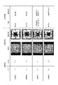
- FIG. 6 is a cross-sectional view taken along the line VII-VII of FIG. It is a figure which shows the evaluation result of the semiconductor light emitting element of an Example and a comparative example.
- AlGaN the composition ratio of Group III elements (total of Al (aluminum) and Ga (gallium)) and N (nitrogen). Is 1: 1 and the ratio of the group III elements Al and Ga is assumed to mean an indefinite arbitrary compound. Further, “AlGaN” may contain In within 5% of the total of Al and Ga as group III elements even if there is no description about In (indium) which is a group III element.
- the Al composition ratio is x 0
- the In composition ratio is y 0 (0 ⁇ y 0 ⁇ 0.05)
- Al x0 In y0 Ga 1-x0-y0 N When simply referred to as "AlN (aluminum nitride)" or “GaN (gallium nitride)", it means that AlN does not contain Ga and GaN does not contain Al, but unless otherwise specified, it is simply "Al”.
- AlGaN does not exclude that it is either AlN or GaN.
- the value of the Al composition ratio can be measured by photoluminescence measurement, X-ray diffraction measurement, or the like.
- a layer that electrically functions as a p-type is referred to as a p-type layer
- a layer that electrically functions as an n-type is referred to as an n-type layer.
- a specific impurity such as Mg (magnesium) or Si (silicon)
- i-type or "undoped”.
- the undoped layer may contain unavoidable impurities during the manufacturing process, and specifically, when the carrier density is small (for example, less than 4 ⁇ 10 16 / cm 3 ), it is referred to as “undoped” in the present specification.
- the values of the concentration of impurities such as Mg and Si are based on SIMS analysis.
- each of the thicknesses of each layer can be calculated by observing the cross section of the growth layer with a transmission electron microscope when the composition of each adjacent layer is sufficiently different (for example, when the Al composition ratio is different by 0.01 or more).
- the boundary and thickness of the layers having the same or almost the same Al composition ratio (for example, less than 0.01) but different impurity concentrations are the boundary between the two and the thickness of each layer.
- the measurement is based on TEM-EDS.
- the impurity concentrations of both can be measured by SIMS analysis.
- the thickness of each layer is thin as in the superlattice structure, the thickness can be measured by using TEM-EDS.
- the semiconductor light emitting element includes a p-type semiconductor layer, a p-type electrode provided on the p-type semiconductor layer, and a pad provided on the p-type electrode, and the p-type electrode is a p-type electrode. It has at least an ohmic metal layer arranged on the type semiconductor layer side and a barrier layer arranged on the pad side of the ohmic metal layer and including a TiN layer.
- the surface diffusion suppressing surface in the top view is defined as the surface diffusion suppressing surface in the top view, the surface diffusion suppressing surface is formed in an annular shape.
- FIG. 1 shows an example of a semiconductor light emitting device 100 (hereinafter referred to as a light emitting device 100) according to the present embodiment.
- the light emitting element 100 is provided on a substrate 10 made of sapphire, an AlN single crystal, or the like, an n-type semiconductor layer 11 which is a layer of an n-type AlGaN-based semiconductor provided on the substrate 10, and an n-type semiconductor layer 11.
- the layered p-type electrode 2 provided on the p-type semiconductor layer 13, and the p-type electrode 2.
- the light emitting element 100 also has an n-type ohmic electrode 91 provided on the n-type semiconductor layer 11, a Pt-containing layer 92 on the n-type ohmic electrode 91, and an n-side pad 94.
- the case where the light emitting element 100 is a horizontal element is shown.
- the pads 4 and 94 on the p side and the n side are connected to the wiring of the electronic board (pad of the electronic board, etc.) and the bonding material, respectively.
- the bonding material 5 containing Ag is arranged on the pad 4 on the p side
- the bonding material 95 containing Ag is arranged on the pad 94 on the n side, and each is bonded to an external wiring.
- the connection structure is adopted.
- a protective film 6 is formed between the pads 4 and 94 on the p side and the n side so that a current flows through the light emitting layer 12.
- the light emitting layer 12 and the p-type semiconductor layer 13 and the n-type ohmic electrode 91 are separated from each other by an n-type layer protective film forming region 11a so as not to cause a short circuit.
- the influence of the migration of Ag further extends from the p-type electrode 2 to the light emitting layer 12, and the Ag becomes a p-type layer and an n-type layer. Shortening the interval may cause non-light emission of the light emitting element 100.
- the pad 4 due to the connection structure of the p-type electrode 2, the Pt-containing layer 3 and the pad 4, as will be described later, the pad 4, the Pt-containing layer 3 and the p-type semiconductor layer 13 of the Ag of the joining material 5 are used. Migration to the light emitting layer 12 via the above is suppressed. As a result, the light emitting element 100 suppresses adverse effects such as discoloration of the p-type electrode 2 and non-light emission of the light emitting layer 12.
- the p-type semiconductor layer 13 is a layer formed of a p-type AlGaN-based semiconductor, and is a so-called p-type contact layer.
- the p-type electrode 2 is arranged on one surface of the p-type semiconductor layer 13.
- the light emitting layer 12 is arranged on the other surface of the p-type semiconductor layer 13.
- the p-type semiconductor layer 13 forms ohmic contact with the p-type electrode 2.
- the p-type semiconductor layer 13 preferably has high conductivity.
- the p-type semiconductor layer 13 may be doped with p-type impurities at a high concentration. This increases the conductivity.
- the Al composition of the p-type semiconductor layer 13 is x, it is preferably 0 ⁇ x ⁇ 0.5.
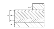
- the p-type electrode 2 has an ohmic metal layer 21 and a barrier layer 22 containing TiN.
- the ohmic metal layer 21 (also referred to as a p-type ohmic electrode) is arranged on the p-type semiconductor layer 13 side of the barrier layer 22.
- the barrier layer 22 is arranged closer to the pad 4 than the ohmic metal layer 21.
- the region of the ohmic metal layer 21 is a barrier when viewed from a bird's-eye view (when the surface of the p-type electrode 2 is viewed vertically from the pad 4 side, it may be referred to as a top view below). It overlaps with the area of layer 22.
- the region of the ohmic metal layer 21 may be a relationship including the region of the barrier layer 22. That is, in top view, the region of the barrier layer 22 may completely overlap or be included in the region of the ohmic metal layer 21.
- the ohmic metal layer 21 a known metal combination can be used as long as it is a metal layer capable of forming ohmic contact with the p-type semiconductor layer 13.
- the ohmic metal layer 21 preferably contains Ni (nickel) and Au (gold) as an example.
- the ohmic metal layer 21 is formed by forming a Ni layer on the p-type semiconductor layer 13 and further forming an Au layer on the Ni layer by vapor deposition or sputtering.
- the ohmic metal layer 21 may contain Rh (rhodium). It is also preferable that the ohmic metal layer 21 is composed of, for example, Ni (nickel) and Rh (rhodium). It is also preferable to have a configuration composed of Ni (nickel), Rh (rhodium) and Au (gold). It is an object of the present invention to suppress adverse effects such as discoloration of the p-type electrode 2 and non-emission of the light emitting layer 12. Therefore, the ohmic metal layer 21 in contact with the p-type semiconductor layer 13 is not intentionally contained with a metal (Ag, Al, etc.) that causes an adverse effect. That is, when the ohmic metal layer 21 contains Ag or Al, it is excluded from the present embodiment.
- the barrier layer 22 is a layer containing at least the TiN layer 222.
- the barrier layer 22 may include, as a layer other than the TiN layer, a metal layer made of a metal that can obtain adhesion to the TiN layer.
- Ti is an example of a metal that can obtain adhesion to the TiN layer. It is more preferable that the TiN layer 222 included in the barrier layer 22 is located at a position sandwiched between the Ti layers so that the Ti layer, the TiN layer and the Ti layer are laminated in this order.
- the thickness of the TiN layer 222 is preferably 100 nm or more and 2000 nm or less, and more preferably 500 nm or more and 1500 nm or less. As a result, migration of Ag can be suppressed. If the thickness of the TiN layer 222 is less than 100 nm, the effect of suppressing Ag migration may be small. When the thickness of the TiN layer 222 exceeds 2000 nm, the electrical resistance of the p-type electrode 2 may increase (so-called forward voltage increase may occur).
- the barrier layer 22 preferably has a Ti layer on its surface. Thereby, the oxidation of the barrier layer 22 can be suppressed. Further, the bondability between the barrier layer 22 and another metal or the protective film 6 can be maintained.
- the barrier layer 22 of the present embodiment includes the first Ti layer 221 which is a layer of Ti formed on the surface of the TiN layer 222 on the ohmic metal layer 21 side in addition to the TiN layer 222.
- the TiN layer 222 has a second Ti layer 223, which is a layer of Ti formed on the surface of the pad 4 side, and the surfaces of the barrier layer 22 on the ohmic metal layer 21 side and the pad 4 side are made of Ti. It is the surface of the layer. That is, the surfaces of the barrier layer 22 on the ohmic metal layer 21 side and the pad 4 side are the surfaces of the Ti layer.
- the thickness of the metal layer (second Ti layer 223 in this embodiment) on the surface of the TiN layer 222 on the pad 4 side in the barrier layer 22 is sufficiently thin. As a result, migration of Ag can be suppressed.
- the thickness of the metal layer on the surface of the TiN layer 222 on the pad 4 side is preferably 1 nm or more and 20 nm or less, and more preferably 5 nm or more and 15 nm or less.
- the TiN layer 222 having a certain thickness has a high effect of suppressing the migration of Ag penetrating the inside of the layer.
- migration of Ag may occur via the side surface.
- the inventors paying attention to these factors to suppress the migration of Ag penetrating the inside of the layer, and further to suppress the migration of Ag that has been inhibited from the migration penetrating the inside of the layer toward the side surface. I thought it was.
- the movement of Ag along the surface of the TiN layer 222 is considered to be slower than the movement of Ag in other metals. Therefore, the inventors suppressed the migration of Ag to the ohmic metal layer 21 and the light emitting layer 12 by forming the surface diffusion suppressing surface S, which will be described later, on the barrier layer 22.
- the thickness of the metal layer on the surface of the TiN layer 222 on the pad 4 side exceeds 20 nm, Ag can move in the direction of the side surface by using the metal layer, as described above. It is not desirable to have a thick metal layer on top of the TiN layer 222.
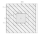
- a region in which the Pt-containing layer 3 and the pad 4 are not formed is secured on the surface of the barrier layer 22 on the pad 4 side (the surface of the second Ti layer 223 or the TiN layer 222 described above).
- a surface diffusion suppressing surface S the region on the surface of the barrier layer 22 on the pad 4 side where the Pt-containing layer 3 and the pad 4 are not formed.
- the surface diffusion suppressing surface S By forming the surface diffusion suppressing surface S, migration of Ag along the surface of the barrier layer 22 can be suppressed.
- the second Ti layer 223 is exposed on the surface diffusion suppressing surface S, and the entire surface of the surface diffusion suppressing surface S is a Ti surface.
- the TiN layer 222 suppresses deterioration such as oxidation. Thereby, the barrier function of the barrier layer 22 can be maintained.
- the barrier layer 22 is not affected by heating for forming ohmic contact between the ohmic metal layer 21 and the p-type semiconductor layer 13. Therefore, it is preferable that the heating for forming the ohmic contact is applied only to the ohmic metal layer 21. Further, it is preferable that the heating is performed before the formation of the barrier layer 22.
- the pad 4 is formed on the barrier layer 22, that is, on the opposite side of the p-type semiconductor layer 13 in the p-type electrode 2.
- the pad 4 is for joining the joining material 5 or forming the joining material 5 on the surface thereof.
- the pad 4 is preferably a metal having adhesion to the joining material 5 containing Ag and having oxidation resistance.
- the pad 4 is preferably composed mainly of a platinum group such as Pt or Pd (palladium).
- metals such as Ti, Ni, Cr (chromium) and Sn (tin) may be partially contained.
- a Pt-containing layer 3 may be arranged between the barrier layer 22 and the pad 4.
- the Pt-containing layer 3 is arranged between the barrier layer 22 and the pad 4.
- the Pt-containing layer 3 overlaps with the pad 4 in top view.
- the Pt-containing layer 3 is smaller than the pad 4 in the top view and is surrounded by the region of the pad 4.
- the Pt-containing layer 3 is, for example, a metal layer in which a Ti layer, a Pt layer, an Au layer, and a Ti layer are laminated in this order.
- the Pt-containing layer 3 has a thickness of more than 20 nm.
- the region of the Pt-containing layer 3 is included in the region of the barrier layer 22 in the top view.
- the region of the Pt-containing layer 3 is surrounded by the region of the barrier layer 22 in the top view.
- the Pt-containing layer may have the effect of inhibiting the diffusion of metals other than Ag by Pt, and may have metals such as Ti, Ni, and Au other than Pt.
- the joining material 5 may contain Ag and may be any material that can obtain an electrical connection between the pad and the wiring of the electronic board (such as the pad of the electronic board).
- solder containing Ag examples include pastes containing Ag powder.
- Sn-Ag-Cu solder SN96CI manufactured by Nippon Superior Co., Ltd.
- SN97C manufactured by Nippon Superior Co., Ltd. can be used as the solder
- DD-1760L manufactured by Kyoto Elex Co., Ltd. can be used as the paste containing Ag powder.
- the pad portion 4a is a surface portion of the pad 4 that is electrically connected to the layer on the side of the barrier layer 22.
- the Pt-containing layer 3 described above is interposed between the pad 4 and the barrier layer 22.
- the pad portion 4a of the pad 4 and the Pt-containing layer 3 are adjacent to each other, and the pad 4 is electrically connected to the barrier layer 22 via the Pt-containing layer 3.
- the joint surface of the pad 4 with the Pt-containing layer 3 is the pad portion 4a.
- the Pt-containing layer 3 is defined as an electrical connection region (hereinafter, may be simply referred to as a connection region) with the layer on the side of the barrier layer 22 in the pad 4.
- the pad 4 has a shape in which the area of the pad portion 4a is smaller than the area of the surface to which the joining material 5 is joined.
- the surface diffusion suppressing surface S is formed, for example, so that at least the pad portion 4a is included in the region of the barrier layer 22 in the top view.
- the outer peripheral portion of the surface of the barrier layer 22 on the pad 4 side can be formed so as not to overlap with the pad portion 4a in the top view and to be exposed from the pad portion 4a.
- the light emitting element 100 may form an insulating protective film 6 that covers the outer periphery and the surface of the barrier layer 22.
- the barrier layer 22 may be in contact with the protective film 6 on the surface diffusion suppressing surface S.
- the protective film 6 is formed of a dielectric such as Si ⁇ 2 (silicon dioxide) or SiN (silicon nitride). The protective film also prevents Ag from moving through the film.
- the region where the barrier layer 22 is exposed from the protective film 6 (the region planned to be the connection region with the pad 4 on the barrier layer 22 side) is the barrier in the top view. It is included in the region of the layer 22. Then, the surface diffusion suppressing surface S may be formed by forming the pad 4 on the barrier layer 22 so as to connect only in the region where the barrier layer 22 is exposed from the protective film 6.
- the surface diffusion suppressing surface S includes the region of the barrier layer 22 and the connection region in which the Pt-containing layer 3 as a metal formed on the barrier layer 22 is in contact with the barrier layer 22. are doing. That is, the surface diffusion suppressing surface S is a portion of the region of the barrier layer 22 that does not overlap with the connection region in the top view.
- the surface diffusion suppressing surface S is secured as an annular (ring-shaped, hollow-shaped) region excluding this connection region from the region of the barrier layer 22. In other words, the connection region in which the Pt-containing layer 3 is in contact with the barrier layer 22 is surrounded by the region of the barrier layer 22 over the entire circumference in the top view.
- the region of the Pt-containing layer 3 is surrounded by the region of the barrier layer 22 over the entire circumference in the top view. Further, the pad portion 4a is surrounded by the region of the Pt-containing layer 3 over the entire circumference in the top view.
- the shortest width w of the surface diffusion suppressing surface S means the shortest width of the annular region in the in-plane direction (diameter direction). In the present embodiment, the shortest distance between the outer peripheral edge of the connection region where the Pt-containing layer 3 is in contact with the barrier layer 22 and the outer peripheral edge of the region of the barrier layer 22 is the shortest width w of the surface diffusion suppressing surface S.
- the shortest width w is preferably wider than the thickness of the TiN layer 222 of the barrier layer 22, and is preferably 3 ⁇ m or more and 50 ⁇ m or less. If the shortest width w is less than 3 ⁇ m, Ag ions may move on the surface of the barrier layer 22 and cannot be sufficiently suppressed. If the shortest width w exceeds 50 ⁇ m, it may be difficult to design the electrode shape for the chip size (usually, one side of the chip is 300 ⁇ m or more and 2000 ⁇ m or less).
- the light emitting element 100 is formed through the following steps. That is, the method for manufacturing the light emitting element 100 includes at least a p-type electrode forming step of forming the p-type electrode 2 on the p-type semiconductor layer 13 and a pad forming step of forming the pad 4 on the p-type electrode 2. include.
- the p-type electrode forming step includes an ohmic metal layer forming step of forming an ohmic metal layer 21 on the p-type semiconductor layer 13 side and a barrier layer 22 including a TiN layer on the pad 4 side of the ohmic metal layer 21. Includes a barrier layer forming step.
- the p-type electrode 2 is formed in the order of the ohmic metal layer 21 and the barrier layer 22 from the p-type semiconductor layer 13 side.
- the heat treatment necessary for the ohmic metal layer 21 to make ohmic contact with the p-type semiconductor layer 13 side is also performed. The heat treatment is preferably performed before the formation of the barrier layer 22.
- the pad 4 is formed so that the electrical connection region between the pad 4 and the barrier layer 22 is surrounded by the region of the barrier layer 22 in the top view.
- the surface diffusion suppressing surface S is formed in an annular shape by forming the pad 4 so that the connection region of the pad 4 with the barrier layer 22 is included in the region of the barrier layer 22 in the top view.
- the surface diffusion suppressing surface S is thus formed as a region of the barrier layer 22 that does not overlap with the electrical connection region between the pad 4 and the barrier layer 22.
- the light emitting element 100 further etches a part of the p-type semiconductor layer 13 and the light emitting layer 12 to expose a part of the n-type semiconductor layer 11, and an n-type ohmic electrode 91 is placed on the exposed n-type semiconductor layer 11. It is preferable that the p-type electrode 2 is provided on the p-type semiconductor layer 13 and a current is passed between the n-type ohmic electrode 91 and the p-type electrode 2.
- the joint surface of the n-side pad 94 with the Pt-containing layer 92 is shown by the n-side pad portion 94a.
- the n-side pad portion 94a is an electrical connection region with the layer (Pt-containing layer 92) on the n-type ohmic electrode 91 side in the n-side pad 94.
- the ohmic metal layer 21, the barrier layer 22, the Pt-containing layer 3, and the pad 4 can be formed by a sputtering method or a thin-film deposition method.
- the method for producing the TiN layer 222 in the barrier layer 22 can be formed by, for example, a PVD coating method, a CVD method, a sputtering method, or the like.
- a reactive sputtering method in which a pure Ti target is sputtering in an Ar gas atmosphere containing nitrogen gas.
- the light emitting device 100 does not have the Pt-containing layer 3 and has a barrier layer 93 instead of the Pt-containing layer 92 on the n-type ohmic electrode 91.
- the barrier layer 22 is different in that the barrier layer 22 is smaller than the ohmic metal layer 21 in top view. Other than that, it is the same as the first embodiment.
- the first embodiment only the differences from the first embodiment will be described.
- the barrier layer 22 of the p-type electrode 2 is smaller than that of the ohmic metal layer 21 in the top view.
- the region of the ohmic metal layer 21 includes the region of the barrier layer 22, and the barrier layer 22 is surrounded by the region of the ohmic metal layer 21.
- the pad 4 and the barrier layer 22 are adjacent to each other, and they are in contact with each other and are directly electrically connected.
- the joint surface of the pad 4 with the barrier layer 22 is the pad portion 4a.
- the pad portion 4a is defined as an electrical connection region with the layer on the side of the barrier layer 22 in the pad 4.
- the surface diffusion suppressing surface S includes a connection region in which the region of the barrier layer 22 is in contact with the barrier layer 22 as a metal pad 4 formed on the barrier layer 22 in the top view.
- the surface diffusion suppressing surface S is an annular region obtained by removing this connection region from the region of the barrier layer 22 as in the case of the first embodiment.
- the pad portion 4a which is a connection region in which the pad 4 is in contact with the barrier layer 22, is surrounded by the region of the barrier layer 22 over the entire circumference in a top view.
- the shortest distance between the outer peripheral edge of the connection region (pad portion 4a) in which the pad 4 is in contact with the barrier layer 22 and the outer peripheral edge of the region of the barrier layer 22 is the shortest width w of the surface diffusion suppressing surface S. be.
- Example 1 As the light emitting element according to the first embodiment, a light emitting element 100A having the basic shape of the light emitting element 100 of the first embodiment shown in FIG. 1 was created.
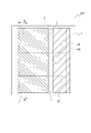
- FIG. 6 shows an example of the arrangement of the p-type electrode 2 and the n-type ohmic electrode 91 of the light emitting element of the first embodiment, the pad portions 4a and 94a on the p-side and the n-side, and the bonding materials 5 and 95 on the p-side and the n-side. Is shown.
- FIG. 7 shows a VII-VII arrow cross section of the light emitting element shown in FIG.
- the light emitting element according to the first embodiment five strips formed by p-type electrodes 2 formed on almost the entire surface of the p-type semiconductor layer 13 are arranged, and n-type ohmics with comb teeth are arranged between them.
- the shape is such that the electrode 91 is inserted, and the n-type layer protective film forming region 11a where the n-type semiconductor layer 11 is exposed without forming an electrode is inserted between the p-type electrode 2 and the n-type ohmic electrode 91. ..
- 94a is similar to the semiconductor light emitting device 100 disclosed in the specification and drawings (FIGS. 1 to 7) of JP-A-2019-106406, and has a size and structure (each ohmic electrode, barrier layer, Pt). It was produced in the same manner except for the composition of the content layer, pad, etc.). Hereinafter, the production conditions for each layer will be described in detail.
- a sapphire substrate (diameter 2 inches, film thickness: 430 ⁇ m, plane orientation: (0001), m-axis direction off angle ⁇ : 0.11 degrees) to be the substrate 10 was prepared.
- an AlN layer having a central thickness of 0.50 ⁇ m (average film thickness of 0.51 ⁇ m) was grown on the sapphire substrate by the MOCVD method to obtain an AlN template substrate.
- the growth temperature of the AlN layer is 1330 ° C.
- the growth pressure in the chamber is 10 Torr
- the growth gas flow rate of ammonia gas and trimethylaluminum (TMA) gas is set so that the ratio of group V / group III is 206. bottom.
- the flow rate of the group V elemental gas (NH 3 ) is 250 sccm, and the flow rate of the group III elemental gas (TMA) is 53 sccm.
- the film thickness of the AlN layer was dispersed at equal intervals including the center of the wafer surface (AlN template substrate) using an optical interference type film thickness measuring device (Nanospec M6100a; manufactured by Nanometrics). A total of 25 film thicknesses were measured.
- the above AlN template substrate was introduced into a heat treatment furnace, and after reducing the pressure to 10 Pa, the nitrogen gas was purged to normal pressure to create a nitrogen gas atmosphere in the furnace, and then the temperature inside the furnace was raised to form an AlN template substrate. It was heat-treated. At that time, the heating temperature was 1650 ° C. and the heating time was 4 hours.
- an undoped AlGaN layer (undoped layer) having a film thickness of 30 nm having an average Al composition ratio of 0.4 was formed as the undoped AlGaN layer by the MOCVD method.
- an n-type semiconductor layer 11 an n-type layer made of Al 0.30 Ga 0.70 N and Si-doped with a film thickness of 2 ⁇ m was formed.
- the Si concentration of the n-type layer was 5.0 ⁇ 10 18 atoms / cm 3 .
- an n-type guide layer having an Al 0.30 Ga 0.70 N and a Si-doped film thickness of 30 nm was formed on the n-type layer, and a 14 nm Al 0.25 Ga 0.75 N was further formed as a barrier layer. ..
- a well layer having a film thickness of 2 nm made of Al 0.10 Ga 0.90 N and a barrier layer made of Al 0.25 Ga 0.75 N having a film thickness of 14 nm were alternately formed, and further, a well layer having a film thickness of 2 nm made of Al 0.10 Ga 0.90 N was formed. A well layer was formed.
- the number of layers of the well layer and the number of layers N of the barrier layer are both 3, the Al composition ratio b of the barrier layer is 0.25, and the Al composition ratio of the well layer is 0.10.
- Si was doped in the formation of the barrier layer.
- an undoped AlGaN guide layer composed of Al 0.25 Ga 0.75 N was formed on the third well layer using nitrogen gas as a carrier gas.
- the film thickness of the AlGaN guide layer was 30 nm.
- TMA trimethylgallium
- the flow rate ratio of TMA gas and TMG gas is changed to form an Mg-doped layer of 235 nm AlGaN clad layer (p-type clad layer) composed of Al 0.20 Ga 0.80 N. Was formed.
- the growth of the AlGaN clad layer was stopped, the carrier gas was switched to nitrogen gas, the gas flow rate was changed to the setting conditions of the p-type GaN contact layer, and then the carrier gas was switched to hydrogen, and Mg was used as the p-type semiconductor layer 13.
- a doped p-type GaN contact layer (p-type contact layer) having a film thickness of 12 nm was formed.
- the Mg concentration of the p-type contact layer was 5.0 ⁇ 10 20 atom / cm 3 on average.
- the growth rate in the thickness direction when forming the p-type contact layer was set to 0.43 ⁇ m / h.
- Table 1 shows the configuration of each layer of the group III nitride semiconductor light emitting device according to Example 1 manufactured as described above.
- a mask is formed on the p-type semiconductor layer 13 and mesa etching is performed by dry etching to expose a part of the n-type semiconductor layer 11 and further on the p-type semiconductor layer 13 from Ni / Rh / Au.
- the p-type ohmic electrode was formed as an ohmic metal layer 21 so that five strips were lined up.
- the film thickness of Ni is 7 nm
- the film thickness of Rh is 50 nm
- the film thickness of Au is 20 nm.
- An n-type ohmic electrode 91 composed of a Ti layer, an Al layer, and a metal layer in which Ti layers are laminated in this order on the n-type semiconductor layer 11 exposed by mesa etching is combed between the strip shapes. It was formed into a comb shape with teeth. At that time, an n-type layer protective film forming region 11a in which the n-type semiconductor layer 11 that does not form an electrode is exposed is provided between the strip shape and the comb teeth (and the outer periphery of the chip).
- the film thickness of Ti is 200 ⁇
- the film thickness of Al is 600 nm
- the film thickness of Ti is 5 nm.
- contact annealing was performed at 550 ° C. to form each electrode.
- a Ti layer (first Ti layer 221), a TiN layer (TiN layer 222), and a Ti layer (second Ti layer) are placed on the p-type ohmic electrode as the ohmic metal layer 21.
- the barrier layer 22 having a layered structure in which 223) was laminated in this order was formed to have the same size as the p-type ohmic electrode.
- the size of one of the strip-shaped p-type ohmic electrodes and the barrier layer 22 as the ohmic metal layer 21 is a strip shape with a long side of 742 ⁇ m and a short side of 94 ⁇ m when viewed from above, and the thickness of the first Ti layer 221. Is 10 nm, the thickness of the TiN layer 222 is 1 ⁇ m, and the thickness of the second Ti layer 223 is 10 nm.
- the first Ti layer 221 of the barrier layer 22 is formed by a sputtering method, and the TiN layer 222 is formed by a reactive sputtering method. It was formed by sputtering in 9 sccm), then the nitrogen gas was stopped, and the second Ti layer 223 was formed again by the sputtering method.
- a Pt-containing layer 3 in which a Ti layer, a Pt layer, an Au layer, and a Ti layer were laminated in this order was formed on the barrier layer 22.
- the Pt-containing layer 3 was formed so as to be surrounded by the barrier layer 22 when viewed from above.
- the portion where the Pt-containing layer 3 is not formed is the surface diffusion suppressing surface S.
- the size of the Pt-containing layer 3 is a rectangular shape having a long side of 734 ⁇ m and a short side of 86 ⁇ m when viewed from above.
- the shortest width w of the surface diffusion suppressing surface S was 4 ⁇ m.
- the film thicknesses of the Ti layer, the Pt layer, the Au layer, and the Ti layer in the Pt-containing layer 3 are 50 nm, 50 nm, 500 nm, and 10 nm in this order.
- a Pt-containing layer 92 in which a Ti layer, a Pt layer, an Au layer, and a Ti layer are laminated in this order on the comb-shaped main body of the n-type ohmic electrode 91 (in the vertical direction of the direction of the comb teeth). Formed.
- the Pt-containing layer 92 was formed at the same time as the Pt-containing layer 3.
- a protective film 6 (thickness 1 ⁇ m) made of SiO 2 was formed on the entire surface, and the protective film 6 on the upper surface of the Pt-containing layer 3 was removed by BHF to be exposed.
- the exposed region (the portion where the pad portion 4a is formed) was formed to have a size smaller than that of the Pt-containing layer 3. Its size is a strip shape with a long side of 329 ⁇ m and a short side of 72 ⁇ m.
- a pad 4 in which a Ti layer, an Au layer, a Ti layer, a Pt layer, and an Au layer are laminated in this order was formed in the exposed Pt-containing layer 3 region.
- the protective film 6 is protected so as to connect the pad portion 4a of each strip across the n-type ohmic electrode 91 and the n-type layer protective film forming region 11a between the strips.
- a pad 4 was also formed on a part of the film 6.
- the film thickness of Ti is 10 nm
- the film thickness of Au is 100 nm
- the film thickness of Ti is 150 nm
- the film thickness of Pt is 100 nm
- the film thickness of Au is 2500 nm.
- n-side pad 94a Similar to the case of forming the pad 4, a region (a portion where the n-side pad portion 94a is formed) exposed by removing the protective film 6 (see FIG. 1) by BHF is also formed on the n-side Pt-containing layer 92. ) Was formed through the n-side pad 94, and Sn-Ag-Cu solder paste was applied as the bonding material 95. At that time, similarly to the pad 4, the n-side pad 94 was also formed on a part of the protective film 6. Similar to the pad 4, the n-side pad 94a has the n-side pad portion 94a of the n-side pad 94 in contact with the Pt-containing layer 92 (see FIG. 1) to form an electrical connection region.
- the chip size is a rectangular shape of 1000 ⁇ m ⁇ 1000 ⁇ m.
- Example 2 As the light emitting element according to the second embodiment, a light emitting element 100A having the basic shape of the light emitting element 100 of the second embodiment shown in FIG. 2 was created.
- the light emitting element 100A according to the second embodiment was created in the same manner as in the first embodiment except as described below.
- a barrier layer 22 having the same layer structure as in Example 1 was formed in a strip shape having a size smaller than that of the p-type ohmic electrode as the ohmic metal layer 21 (long side 734 ⁇ m ⁇ short side 86 ⁇ m). Then, the Pt-containing layer 3 was not formed on the barrier layer 22, and a protective film (thickness 1 ⁇ m) made of SiO 2 was formed on the entire surface of the barrier layer 22 on the second Ti layer 223 side. After that, the protective film in the inner portion of the surface region of the barrier layer 22 where the surface diffusion suppressing surface S was planned to be formed was removed by BHF and exposed. The size of the exposed region (the portion where the pad portion 4a is formed) was a strip shape having a long side of 329 ⁇ m and a short side of 72 ⁇ m, and the pad 4 was formed on the exposed barrier layer 22.
- the metal formed on the n-type ohmic electrode 91 is replaced with the Pt-containing layer 92 of Example 1, and the barrier layer 93 (see FIG. 4) in which the Ti layer, the TiN layer, and the Ti layer are laminated in this order. ).
- the barrier layer 93 was formed at the same time as the barrier layer 22. Then, it was separated into the chip-shaped light emitting element (light emitting element 100A) according to the second embodiment in the same manner as in the first embodiment.
- the shortest width w of the surface diffusion suppressing surface S was 7 ⁇ m.
- Example 3 The chip-shaped light emitting device (light emitting device 100A) in Example 3 was produced in the same manner as in Example 1 except that the thickness of the TiN layer 222 in the barrier layer 22 was changed from 1 ⁇ m to 500 nm.
- Example 4 The chip-shaped light emitting device (light emitting device 100A) in Example 4 was produced in the same manner as in Example 2 except that the thickness of the TiN layer 222 in the barrier layer 22 was changed from 1 ⁇ m to 500 nm.
- Comparative Example 1 The same as in Example 1 except that a metal layer (barrier layer not including the TiN layer) in which a Pt layer, an Au layer, and a Ti layer are laminated in this order is formed instead of the barrier layer 22 of the first embodiment. Therefore, a chip-shaped light emitting device according to Comparative Example 1 was produced.
- the film thickness of Pt is 50 nm
- the film thickness of Au is 100 nm
- the film thickness of Ti is 5 nm.
- Comparative Example 2 On the barrier layer similar to the barrier layer 22 of Example 1, a Pt-containing layer having the same layer structure as that of the Pt-containing layer 3 of Example 1 was formed at the same center as the barrier layer 22 (that is, on the surface).
- the chip-shaped light emitting device according to Comparative Example 2 was produced in the same manner as in Example 1 except that the diffusion suppression surface was not secured). That is, in the chip of Comparative Example 2, the entire surface of the barrier layer on the Pt-containing layer side is covered with the Pt-containing layer, and the surface diffusion suppressing surface S does not exist.
- Table 2 shows a list of the laminated structure of the light emitting elements of Examples 1 and 2 and Comparative Examples 1 and 2 and the presence or absence of the surface diffusion suppressing surface.
- a light emitting element having a forward voltage close to the average value of the respective forward voltages was selected as a representative, and the temperature was 290 ° C. on the hot plate. The appearance of the electrode after heating for 3 minutes was observed using a metallurgical microscope, and the emission output was confirmed. Further, except for Comparative Example 1 in which there was a change when heated at 290 ° C. for 3 minutes, in Examples 1 and 2 and Comparative Example 2 in which there was no change at 290 ° C., the temperature was additionally raised to 320 ° C. 3 After heating for a minute, the appearance of the electrode and the emission output were observed.
- the light emitting element of Comparative Example 1 was heated to 290 ° C., and the light emitting elements of Examples 1 and 2 and Comparative Example 2 were heated to 320 ° C.
- the photograph of the whole image of the above, and the findings (state after heating) regarding the appearance of the electrode and the whole image of the light emitting element are also shown in the table of FIG.
- Comparative Example 2 the reason why the migration of Ag, which causes non-emission (short), could not be suppressed in Comparative Example 2 is due to the relationship between the thickness of the barrier layer and the shortest width of the surface diffusion suppressing surface. That is, in Comparative Example 2, the distance corresponding to the thickness (1 ⁇ m) of the end surface of the TiN layer of the barrier layer is for Ag moving on the surface (side surface) even if it cannot penetrate the barrier layer. It is probable that was a distance that could be exceeded. Therefore, it is preferable to have the shortest width of the surface diffusion suppressing surface larger than the thickness of the barrier layer.
- the present invention can be applied to a semiconductor light emitting device, a semiconductor light emitting device connection structure, and a method for manufacturing a semiconductor light emitting device.
Landscapes
- Led Devices (AREA)
- Electrodes Of Semiconductors (AREA)
Abstract
Description
p型AlGaN系半導体層と、
前記p型AlGaN系半導体層上に設けられたp型電極と、
前記p型電極上に設けられたパッドと、
を備え、
前記p型電極は、
前記p型AlGaN系半導体層側に配置されたオーミック金属層と、
前記オーミック金属層よりも前記パッド側に配置され、TiN層を含むバリア層と、
を有し、
上面視において、前記バリア層の領域のうち、前記パッドと前記バリア層との電気的な接続領域と重複していない領域を表面拡散抑制面と定義した場合、前記表面拡散抑制面が環状に形成されている。
前記オーミック金属層は、Agを含まない層であってもよい。
上面視において、前記バリア層の領域が、前記オーミック金属層の領域に完全に重複又は包含されてもよい。
前記バリア層に含まれるTiN層の厚さが、100nm以上2000nm以下であってもよい。
前記バリア層が更にTi層を有し、前記表面拡散抑制面には前記Ti層が露出してもよい。
前記バリア層と前記パッドの間に配置されたPt含有層を更に備え、
前記パッドと前記バリア層との電気的な接続が、前記Pt含有層を介して行われ、
上面視において、前記Pt含有層の領域が前記表面拡散抑制面に囲まれていてもよい。
前記オーミック金属層はNiとAuを含んでもよい。
上面視において、前記接続領域の外周縁と前記バリア層の領域の外周縁との最短距離が3~50μmであってもよい。
前記バリア層は、前記パッドから前記p型AlGaN系半導体層へのAgのマイグレーションを抑制するものであってよい。
Agを含む接合材と、上述の半導体発光素子と、を含み、
前記接合材は、前記半導体発光素子の前記パッド上に形成されている。
p型AlGaN系半導体層上に、p型電極を形成するp型電極形成工程と、
前記p型電極上にパッドを形成するパッド形成工程と、を含み、
前記p型電極形成工程は、
前記p型AlGaN系半導体層側にオーミック金属層を形成するオーミック金属層形成工程と、
前記オーミック金属層よりも前記パッド側に、TiN層を含むバリア層を形成するバリア層形成工程と、を含み、
上面視において、前記バリア層の領域のうち、前記パッドと前記バリア層との電気的な接続領域と重複させない領域を表面拡散抑制面と定義した場合、前記パッド形成工程は、前記表面拡散抑制面が環状に形成されるように前記パッドを形成する。
前記オーミック金属層形成工程は、Agを含まない前記オーミック金属層を形成するものであってよい。
前記バリア層形成工程は、上面視において、前記バリア層の領域を前記オーミック金属層の領域に完全に重複又は包含させてよい。
前記バリア層形成工程は、前記TiN層とTi層を含む前記バリア層を形成し、前記表面拡散抑制面に前記Ti層を露出させてよい。
〔全体構成の説明〕
図1に、本実施形態に係る半導体発光素子100(以下、発光素子100と記載する)の一例を示す。発光素子100は、サファイアやAlN単結晶等で形成された基板10、基板10上に設けられたn型AlGaN系半導体の層であるn型半導体層11、n型半導体層11上に設けられた発光層12、n型半導体層11上に設けられ、発光層12上に設けられたp型半導体層13、p型半導体層13上に設けられた層状のp型電極2、p型電極2上に設けられたPt含有層3及びPt含有層3を介してp型電極2上に設けられたパッド4を備えている。発光素子100は、その他、n型半導体層11上に設けられたn型オーミック電極91、n型オーミック電極91上のPt含有層92、及びn側パッド94を有する。本実施形態では、一例として、発光素子100が横型の素子である場合を示している。
p型半導体層13は、p型AlGaN系半導体で形成された層であり、いわゆるp型コンタクト層である。p型半導体層13の一方の面上にはp型電極2が配置される。p型半導体層13の他方の面上には発光層12が配置される。p型半導体層13は、p型電極2とオーミックコンタクトを形成する。p型半導体層13は、導電性が高いことが好ましい。p型半導体層13は、p型不純物を高濃度にドーピングされていても良い。これにより導電性が高くなる。p型半導体層13のAl組成をxとした場合、0≦x≦0.5であることが好ましい。
第二実施形態は、図4に示すように、発光素子100がPt含有層3を有さない点、及び、n型オーミック電極91上においてPt含有層92に代えてバリア層93を有する点で第一実施形態と異なる。また、図4、図5に示すように、バリア層22が、上面視においてオーミック金属層21よりも小さい点で異なる。それ以外は第一実施形態と同じである。以下では第一実施形態との相違点についてのみ説明する。
実施例1に係る発光素子として、図1に示す第一実施形態の発光素子100を基本形状とした発光素子100Aを作成した。図6には、実施例1の発光素子のp型電極2及びn型オーミック電極91、p側及びn側のパッド部4a、94a、p側及びn側の接合材5、95の配置の一例を示している。

実施例2に係る発光素子として、図2に示す第二実施形態の発光素子100を基本形状とした発光素子100Aを作成した。実施例2に係る発光素子100Aは、以下に説明する以外は実施例1と同様にして作成した。
バリア層22におけるTiN層222の厚さを、1μmから500nmに変えた以外は、実施例1と同様にして、実施例3におけるチップ状の発光素子(発光素子100A)を作製した。
バリア層22におけるTiN層222の厚さを、1μmから500nmに変えた以外は、実施例2と同様にして、実施例4におけるチップ状の発光素子(発光素子100A)を作製した。
実施例1のバリア層22に替えて、Ptの層、Auの層及びTiの層をこの順に積層させた金属層(TiN層を含まないバリア層)を形成した以外は実施例1と同様にして、比較例1に係るチップ状の発光素子を作製した。Ptの膜厚は50nm、Auの膜厚は100nm、Tiの膜厚は5nmである。
実施例1のバリア層22と同様のバリア層に、実施例1のPt含有層3と同様の層構造のPt含有層を、バリア層22と中心を同じく、同じサイズで形成した(すなわち、表面拡散抑制面を確保しなかった)以外は実施例1と同様にして比較例2に係るチップ状の発光素子を作製した。すなわち、比較例2のチップではPt含有層側のバリア層の全面がPt含有層で覆われており、表面拡散抑制面Sが存在しない。

実施例1,2及び比較例1,2で得られた発光素子(測定個数24個)に対して、定電流電圧電源を用いて電流600mAを通電し、発光出力及び順方向電圧(Vf)を測定し、それらの平均値を出した。その結果の表を図8に示す。
3 :Pt含有層
4 :パッド
4a :パッド部
5 :接合材
6 :保護膜
10 :基板
11 :n型半導体層
11a :n型層保護膜形成領域
12 :発光層
13 :p型半導体層
21 :オーミック金属層
22 :バリア層
91 :n型オーミック電極
92 :Pt含有層
93 :バリア層
94 :n側パッド
94a :n側パッド部
95 :接合材
100 :発光素子(半導体発光素子)
100A :発光素子
221 :第一Ti層
222 :TiN層
223 :第二Ti層
S :表面拡散抑制面
w :最短幅
Claims (14)
- p型AlGaN系半導体層と、
前記p型AlGaN系半導体層上に設けられたp型電極と、
前記p型電極上に設けられたパッドと、
を備え、
前記p型電極は、
前記p型AlGaN系半導体層側に配置されたオーミック金属層と、
前記オーミック金属層よりも前記パッド側に配置され、TiN層を含むバリア層と、
を有し、
上面視において、前記バリア層の領域のうち、前記パッドと前記バリア層との電気的な接続領域と重複していない領域を表面拡散抑制面と定義した場合、前記表面拡散抑制面が環状に形成されている半導体発光素子。 - 前記オーミック金属層は、Agを含まない層である請求項1に記載の半導体発光素子。
- 上面視において、前記バリア層の領域が、前記オーミック金属層の領域に完全に重複又は包含されている請求項1に記載の半導体発光素子。
- 前記バリア層に含まれるTiN層の厚さが、100nm以上2000nm以下である請求項1に記載の半導体発光素子。
- 前記バリア層が更にTi層を有し、前記表面拡散抑制面には前記Ti層が露出している請求項1に記載の半導体発光素子。
- 前記バリア層と前記パッドの間に配置されたPt含有層を更に備え、
前記パッドと前記バリア層との電気的な接続が、前記Pt含有層を介して行われ、
上面視において、前記Pt含有層の領域が前記表面拡散抑制面に囲まれている請求項1に記載の半導体発光素子。 - 前記オーミック金属層はNiとAuを含む請求項1に記載の半導体発光素子。
- 上面視において、前記接続領域の外周縁と前記バリア層の領域の外周縁との最短距離が3~50μmである請求項1から7のいずれか一項に記載の半導体発光素子。
- 前記バリア層は、前記パッドから前記p型AlGaN系半導体層へのAgのマイグレーションを抑制する請求項1に記載の半導体発光素子。
- Agを含む接合材と、請求項1から9に記載の半導体発光素子と、を含み、
前記接合材は、前記半導体発光素子の前記パッド上に形成されている半導体発光素子接続構造。 - p型AlGaN系半導体層上に、p型電極を形成するp型電極形成工程と、
前記p型電極上にパッドを形成するパッド形成工程と、を含み、
前記p型電極形成工程は、
前記p型AlGaN系半導体層側にオーミック金属層を形成するオーミック金属層形成工程と、
前記オーミック金属層よりも前記パッド側に、TiN層を含むバリア層を形成するバリア層形成工程と、を含み、
上面視において、前記バリア層の領域のうち、前記パッドと前記バリア層との電気的な接続領域と重複させない領域を表面拡散抑制面と定義した場合、前記パッド形成工程は、前記表面拡散抑制面が環状に形成されるように前記パッドを形成する半導体発光素子の製造方法。 - 前記オーミック金属層形成工程は、Agを含まない前記オーミック金属層を形成する請求項11に記載の半導体発光素子の製造方法。
- 前記バリア層形成工程は、上面視において、前記バリア層の領域を前記オーミック金属層の領域に完全に重複又は包含させる請求項11に記載の半導体発光素子の製造方法。
- 前記バリア層形成工程は、前記TiN層とTi層を含む前記バリア層を形成し、前記表面拡散抑制面に前記Ti層を露出させる請求項11に記載の半導体発光素子の製造方法。
Priority Applications (4)
| Application Number | Priority Date | Filing Date | Title |
|---|---|---|---|
| DE112021005518.6T DE112021005518T5 (de) | 2020-10-20 | 2021-05-18 | Lichtemittierende halbleitervorrichtung, verbindungsstruktur für eine lichtemittierende halbleitervorrichtung und verfahren zur herstellung einer lichtemittierenden halbleitervorrichtung |
| CN202180071399.0A CN116457947A (zh) | 2020-10-20 | 2021-05-18 | 半导体发光元件、半导体发光元件连接构造和半导体发光元件的制造方法 |
| US18/249,258 US20240030386A1 (en) | 2020-10-20 | 2021-05-18 | Semiconductor light-emitting device, semiconductor light-emitting device connecting structure, and method of producing semiconductor light-emitting device |
| KR1020237012965A KR102799215B1 (ko) | 2020-10-20 | 2021-05-18 | 반도체 발광 소자, 반도체 발광 소자 접속 구조 및 반도체 발광 소자의 제조 방법 |
Applications Claiming Priority (2)
| Application Number | Priority Date | Filing Date | Title |
|---|---|---|---|
| JP2020-176269 | 2020-10-20 | ||
| JP2020176269A JP6890707B1 (ja) | 2020-10-20 | 2020-10-20 | 半導体発光素子及び半導体発光素子の製造方法 |
Publications (1)
| Publication Number | Publication Date |
|---|---|
| WO2022085231A1 true WO2022085231A1 (ja) | 2022-04-28 |
Family
ID=76429616
Family Applications (1)
| Application Number | Title | Priority Date | Filing Date |
|---|---|---|---|
| PCT/JP2021/018867 Ceased WO2022085231A1 (ja) | 2020-10-20 | 2021-05-18 | 半導体発光素子、半導体発光素子接続構造及び半導体発光素子の製造方法 |
Country Status (7)
| Country | Link |
|---|---|
| US (1) | US20240030386A1 (ja) |
| JP (1) | JP6890707B1 (ja) |
| KR (1) | KR102799215B1 (ja) |
| CN (1) | CN116457947A (ja) |
| DE (1) | DE112021005518T5 (ja) |
| TW (1) | TWI836223B (ja) |
| WO (1) | WO2022085231A1 (ja) |
Families Citing this family (3)
| Publication number | Priority date | Publication date | Assignee | Title |
|---|---|---|---|---|
| EP4243095A4 (en) * | 2020-11-06 | 2024-07-31 | LG Electronics Inc. | LIGHT-EMITTING DIODE AND DISPLAY DEVICE THEREOF |
| CN117878212B (zh) * | 2024-03-13 | 2024-06-21 | 山西中科潞安紫外光电科技有限公司 | 一种深紫外led倒装芯片及其制备方法 |
| JP7782090B1 (ja) | 2024-05-31 | 2025-12-08 | Dowaエレクトロニクス株式会社 | n型オーミック電極及びn型オーミック電極の製造方法、並びにIII族窒化物半導体発光素子及びIII族窒化物半導体発光素子の製造方法 |
Citations (13)
| Publication number | Priority date | Publication date | Assignee | Title |
|---|---|---|---|---|
| JP2005210051A (ja) * | 2004-01-19 | 2005-08-04 | Samsung Electro Mech Co Ltd | フリップチップ用窒化物半導体発光素子 |
| JP2006041403A (ja) * | 2004-07-29 | 2006-02-09 | Nichia Chem Ind Ltd | 半導体発光素子 |
| JP2008192782A (ja) * | 2007-02-05 | 2008-08-21 | Toyota Central R&D Labs Inc | 電極及びそれを有するiii族窒化物系化合物半導体発光素子 |
| WO2012026068A1 (ja) * | 2010-08-24 | 2012-03-01 | パナソニック株式会社 | 発光素子 |
| JP2012142401A (ja) * | 2010-12-28 | 2012-07-26 | Showa Denko Kk | 半導体チップの製造方法および半導体ウエハの分割方法 |
| WO2014109137A1 (ja) * | 2013-01-11 | 2014-07-17 | Dowaエレクトロニクス株式会社 | 発光素子及びその製造方法 |
| JP2014207327A (ja) * | 2013-04-12 | 2014-10-30 | スタンレー電気株式会社 | 半導体発光素子 |
| JP2014241401A (ja) * | 2013-05-17 | 2014-12-25 | 日亜化学工業株式会社 | 半導体発光素子およびその製造方法 |
| JP2015035510A (ja) * | 2013-08-09 | 2015-02-19 | 日亜化学工業株式会社 | 発光素子 |
| US20160111602A1 (en) * | 2014-03-07 | 2016-04-21 | Lextar Electronics Corporation | Light-emitting diode chip |
| CN105552191A (zh) * | 2016-02-02 | 2016-05-04 | 厦门乾照光电股份有限公司 | 能增进横向电流扩散并拥有双反射表面的led芯片电极结构 |
| JP2017108005A (ja) * | 2015-12-10 | 2017-06-15 | ウシオ電機株式会社 | 半導体発光素子及びその製造方法 |
| JP2020145316A (ja) * | 2019-03-06 | 2020-09-10 | 豊田合成株式会社 | 半導体装置 |
Family Cites Families (5)
| Publication number | Priority date | Publication date | Assignee | Title |
|---|---|---|---|---|
| KR100764450B1 (ko) * | 2006-11-15 | 2007-10-05 | 삼성전기주식회사 | 플립칩형 질화물 반도체 발광소자 |
| JP5886615B2 (ja) | 2011-11-30 | 2016-03-16 | スタンレー電気株式会社 | 半導体素子 |
| US9941384B2 (en) * | 2015-08-29 | 2018-04-10 | Taiwan Semiconductor Manufacturing Co., Ltd. | Semiconductor device and method for fabricating the same |
| KR101826950B1 (ko) * | 2016-07-29 | 2018-02-07 | 서울바이오시스 주식회사 | 솔더 페이스트를 통해 접착된 발광 다이오드를 갖는 발광 다이오드 모듈 및 발광 다이오드 |
| JP2019106406A (ja) | 2017-12-08 | 2019-06-27 | Dowaエレクトロニクス株式会社 | 半導体発光素子およびそれを用いた表面実装デバイスならびにそれらの製造方法 |
-
2020
- 2020-10-20 JP JP2020176269A patent/JP6890707B1/ja active Active
-
2021
- 2021-05-18 CN CN202180071399.0A patent/CN116457947A/zh active Pending
- 2021-05-18 DE DE112021005518.6T patent/DE112021005518T5/de active Pending
- 2021-05-18 WO PCT/JP2021/018867 patent/WO2022085231A1/ja not_active Ceased
- 2021-05-18 US US18/249,258 patent/US20240030386A1/en active Pending
- 2021-05-18 KR KR1020237012965A patent/KR102799215B1/ko active Active
- 2021-06-09 TW TW110120858A patent/TWI836223B/zh active
Patent Citations (13)
| Publication number | Priority date | Publication date | Assignee | Title |
|---|---|---|---|---|
| JP2005210051A (ja) * | 2004-01-19 | 2005-08-04 | Samsung Electro Mech Co Ltd | フリップチップ用窒化物半導体発光素子 |
| JP2006041403A (ja) * | 2004-07-29 | 2006-02-09 | Nichia Chem Ind Ltd | 半導体発光素子 |
| JP2008192782A (ja) * | 2007-02-05 | 2008-08-21 | Toyota Central R&D Labs Inc | 電極及びそれを有するiii族窒化物系化合物半導体発光素子 |
| WO2012026068A1 (ja) * | 2010-08-24 | 2012-03-01 | パナソニック株式会社 | 発光素子 |
| JP2012142401A (ja) * | 2010-12-28 | 2012-07-26 | Showa Denko Kk | 半導体チップの製造方法および半導体ウエハの分割方法 |
| WO2014109137A1 (ja) * | 2013-01-11 | 2014-07-17 | Dowaエレクトロニクス株式会社 | 発光素子及びその製造方法 |
| JP2014207327A (ja) * | 2013-04-12 | 2014-10-30 | スタンレー電気株式会社 | 半導体発光素子 |
| JP2014241401A (ja) * | 2013-05-17 | 2014-12-25 | 日亜化学工業株式会社 | 半導体発光素子およびその製造方法 |
| JP2015035510A (ja) * | 2013-08-09 | 2015-02-19 | 日亜化学工業株式会社 | 発光素子 |
| US20160111602A1 (en) * | 2014-03-07 | 2016-04-21 | Lextar Electronics Corporation | Light-emitting diode chip |
| JP2017108005A (ja) * | 2015-12-10 | 2017-06-15 | ウシオ電機株式会社 | 半導体発光素子及びその製造方法 |
| CN105552191A (zh) * | 2016-02-02 | 2016-05-04 | 厦门乾照光电股份有限公司 | 能增进横向电流扩散并拥有双反射表面的led芯片电极结构 |
| JP2020145316A (ja) * | 2019-03-06 | 2020-09-10 | 豊田合成株式会社 | 半導体装置 |
Also Published As
| Publication number | Publication date |
|---|---|
| DE112021005518T5 (de) | 2023-08-24 |
| TWI836223B (zh) | 2024-03-21 |
| KR20230070000A (ko) | 2023-05-19 |
| KR102799215B1 (ko) | 2025-04-23 |
| JP2022067526A (ja) | 2022-05-06 |
| TW202218214A (zh) | 2022-05-01 |
| US20240030386A1 (en) | 2024-01-25 |
| JP6890707B1 (ja) | 2021-06-18 |
| CN116457947A (zh) | 2023-07-18 |
Similar Documents
| Publication | Publication Date | Title |
|---|---|---|
| TWI501425B (zh) | Nitride semiconductor device and manufacturing method thereof | |
| JP5045336B2 (ja) | 半導体発光素子 | |
| JP3912044B2 (ja) | Iii族窒化物系化合物半導体発光素子の製造方法 | |
| JP4956928B2 (ja) | 半導体装置 | |
| JP4449405B2 (ja) | 窒化物半導体発光素子およびその製造方法 | |
| JP6890707B1 (ja) | 半導体発光素子及び半導体発光素子の製造方法 | |
| JP7049186B2 (ja) | 半導体発光素子および半導体発光素子の製造方法 | |
| JP2004006498A (ja) | Iii族窒化物系化合物半導体発光素子 | |
| JP5347219B2 (ja) | 半導体発光素子 | |
| US11335830B2 (en) | Photo-emission semiconductor device and method of manufacturing same | |
| WO2006082687A1 (ja) | GaN系発光ダイオードおよび発光装置 | |
| JP3807020B2 (ja) | 発光半導体素子用透光性電極およびその作製方法 | |
| JP5471485B2 (ja) | 窒化物半導体素子および窒化物半導体素子のパッド電極の製造方法 | |
| KR100923034B1 (ko) | 반도체 소자 및 그 제조 방법 | |
| US6653215B1 (en) | Contact to n-GaN with Au termination | |
| KR100538199B1 (ko) | Ⅲ족 질화물계 화합물 반도체 장치를 제조하는 방법 | |
| TWI568024B (zh) | Nitride semiconductor light emitting device and manufacturing method thereof | |
| JPH10335705A (ja) | 窒化ガリウム系化合物半導体素子及びその製造方法 | |
| JP4868821B2 (ja) | 窒化ガリウム系化合物半導体及び発光素子 | |
| TW201715754A (zh) | 半導體發光元件 | |
| JP2005354040A (ja) | 半導体発光素子およびその製法 | |
| JP5734935B2 (ja) | 半導体装置及びその製造方法 | |
| JP5533573B2 (ja) | 半導体素子 | |
| JP2006024913A (ja) | 窒化ガリウム系化合物半導体発光素子用透光性正極および発光素子 | |
| JP2007201046A (ja) | 化合物半導体及び発光素子 |
Legal Events
| Date | Code | Title | Description |
|---|---|---|---|
| 121 | Ep: the epo has been informed by wipo that ep was designated in this application |
Ref document number: 21882375 Country of ref document: EP Kind code of ref document: A1 |
|
| ENP | Entry into the national phase |
Ref document number: 20237012965 Country of ref document: KR Kind code of ref document: A |
|
| WWE | Wipo information: entry into national phase |
Ref document number: 18249258 Country of ref document: US |
|
| WWE | Wipo information: entry into national phase |
Ref document number: 202180071399.0 Country of ref document: CN |
|
| 122 | Ep: pct application non-entry in european phase |
Ref document number: 21882375 Country of ref document: EP Kind code of ref document: A1 |
|
| WWG | Wipo information: grant in national office |
Ref document number: 1020237012965 Country of ref document: KR |