WO2022070588A1 - 磁気素子及び集積装置 - Google Patents
磁気素子及び集積装置 Download PDFInfo
- Publication number
- WO2022070588A1 WO2022070588A1 PCT/JP2021/028497 JP2021028497W WO2022070588A1 WO 2022070588 A1 WO2022070588 A1 WO 2022070588A1 JP 2021028497 W JP2021028497 W JP 2021028497W WO 2022070588 A1 WO2022070588 A1 WO 2022070588A1
- Authority
- WO
- WIPO (PCT)
- Prior art keywords
- layer
- magnetic
- ferromagnetic
- wiring
- spin
- Prior art date
- Legal status (The legal status is an assumption and is not a legal conclusion. Google has not performed a legal analysis and makes no representation as to the accuracy of the status listed.)
- Ceased
Links
Images




Classifications
-
- H—ELECTRICITY
- H10—SEMICONDUCTOR DEVICES; ELECTRIC SOLID-STATE DEVICES NOT OTHERWISE PROVIDED FOR
- H10N—ELECTRIC SOLID-STATE DEVICES NOT OTHERWISE PROVIDED FOR
- H10N52/00—Hall-effect devices
- H10N52/80—Constructional details
-
- H—ELECTRICITY
- H01—ELECTRIC ELEMENTS
- H01F—MAGNETS; INDUCTANCES; TRANSFORMERS; SELECTION OF MATERIALS FOR THEIR MAGNETIC PROPERTIES
- H01F10/00—Thin magnetic films, e.g. of one-domain structure
- H01F10/32—Spin-exchange-coupled multilayers, e.g. nanostructured superlattices
- H01F10/324—Exchange coupling of magnetic film pairs via a very thin non-magnetic spacer, e.g. by exchange with conduction electrons of the spacer
- H01F10/3254—Exchange coupling of magnetic film pairs via a very thin non-magnetic spacer, e.g. by exchange with conduction electrons of the spacer the spacer being semiconducting or insulating, e.g. for spin tunnel junction [STJ]
-
- G—PHYSICS
- G11—INFORMATION STORAGE
- G11B—INFORMATION STORAGE BASED ON RELATIVE MOVEMENT BETWEEN RECORD CARRIER AND TRANSDUCER
- G11B5/00—Recording by magnetisation or demagnetisation of a record carrier; Reproducing by magnetic means; Record carriers therefor
- G11B5/127—Structure or manufacture of heads, e.g. inductive
- G11B5/33—Structure or manufacture of flux-sensitive heads, i.e. for reproduction only; Combination of such heads with means for recording or erasing only
- G11B5/39—Structure or manufacture of flux-sensitive heads, i.e. for reproduction only; Combination of such heads with means for recording or erasing only using magneto-resistive devices or effects
-
- H—ELECTRICITY
- H01—ELECTRIC ELEMENTS
- H01F—MAGNETS; INDUCTANCES; TRANSFORMERS; SELECTION OF MATERIALS FOR THEIR MAGNETIC PROPERTIES
- H01F10/00—Thin magnetic films, e.g. of one-domain structure
- H01F10/08—Thin magnetic films, e.g. of one-domain structure characterised by magnetic layers
- H01F10/10—Thin magnetic films, e.g. of one-domain structure characterised by magnetic layers characterised by the composition
- H01F10/18—Thin magnetic films, e.g. of one-domain structure characterised by magnetic layers characterised by the composition being compounds
- H01F10/193—Magnetic semiconductor compounds
- H01F10/1936—Half-metallic, e.g. epitaxial CrO2 or NiMnSb films
-
- H—ELECTRICITY
- H01—ELECTRIC ELEMENTS
- H01F—MAGNETS; INDUCTANCES; TRANSFORMERS; SELECTION OF MATERIALS FOR THEIR MAGNETIC PROPERTIES
- H01F10/00—Thin magnetic films, e.g. of one-domain structure
- H01F10/32—Spin-exchange-coupled multilayers, e.g. nanostructured superlattices
- H01F10/324—Exchange coupling of magnetic film pairs via a very thin non-magnetic spacer, e.g. by exchange with conduction electrons of the spacer
- H01F10/3268—Exchange coupling of magnetic film pairs via a very thin non-magnetic spacer, e.g. by exchange with conduction electrons of the spacer the exchange coupling being asymmetric, e.g. by use of additional pinning, by using antiferromagnetic or ferromagnetic coupling interface, i.e. so-called spin-valve [SV] structure, e.g. NiFe/Cu/NiFe/FeMn
- H01F10/3272—Exchange coupling of magnetic film pairs via a very thin non-magnetic spacer, e.g. by exchange with conduction electrons of the spacer the exchange coupling being asymmetric, e.g. by use of additional pinning, by using antiferromagnetic or ferromagnetic coupling interface, i.e. so-called spin-valve [SV] structure, e.g. NiFe/Cu/NiFe/FeMn by use of anti-parallel coupled [APC] ferromagnetic layers, e.g. artificial ferrimagnets [AFI], artificial [AAF] or synthetic [SAF] anti-ferromagnets
-
- H—ELECTRICITY
- H01—ELECTRIC ELEMENTS
- H01F—MAGNETS; INDUCTANCES; TRANSFORMERS; SELECTION OF MATERIALS FOR THEIR MAGNETIC PROPERTIES
- H01F10/00—Thin magnetic films, e.g. of one-domain structure
- H01F10/32—Spin-exchange-coupled multilayers, e.g. nanostructured superlattices
- H01F10/324—Exchange coupling of magnetic film pairs via a very thin non-magnetic spacer, e.g. by exchange with conduction electrons of the spacer
- H01F10/329—Spin-exchange coupled multilayers wherein the magnetisation of the free layer is switched by a spin-polarised current, e.g. spin torque effect
-
- H—ELECTRICITY
- H10—SEMICONDUCTOR DEVICES; ELECTRIC SOLID-STATE DEVICES NOT OTHERWISE PROVIDED FOR
- H10B—ELECTRONIC MEMORY DEVICES
- H10B61/00—Magnetic memory devices, e.g. magnetoresistive RAM [MRAM] devices
-
- H—ELECTRICITY
- H10—SEMICONDUCTOR DEVICES; ELECTRIC SOLID-STATE DEVICES NOT OTHERWISE PROVIDED FOR
- H10D—INORGANIC ELECTRIC SEMICONDUCTOR DEVICES
- H10D48/00—Individual devices not covered by groups H10D1/00 - H10D44/00
- H10D48/40—Devices controlled by magnetic fields
-
- H—ELECTRICITY
- H10—SEMICONDUCTOR DEVICES; ELECTRIC SOLID-STATE DEVICES NOT OTHERWISE PROVIDED FOR
- H10N—ELECTRIC SOLID-STATE DEVICES NOT OTHERWISE PROVIDED FOR
- H10N50/00—Galvanomagnetic devices
- H10N50/10—Magnetoresistive devices
-
- H—ELECTRICITY
- H10—SEMICONDUCTOR DEVICES; ELECTRIC SOLID-STATE DEVICES NOT OTHERWISE PROVIDED FOR
- H10N—ELECTRIC SOLID-STATE DEVICES NOT OTHERWISE PROVIDED FOR
- H10N50/00—Galvanomagnetic devices
- H10N50/80—Constructional details
-
- H—ELECTRICITY
- H10—SEMICONDUCTOR DEVICES; ELECTRIC SOLID-STATE DEVICES NOT OTHERWISE PROVIDED FOR
- H10N—ELECTRIC SOLID-STATE DEVICES NOT OTHERWISE PROVIDED FOR
- H10N52/00—Hall-effect devices
- H10N52/80—Constructional details
- H10N52/85—Materials of the active region
-
- H—ELECTRICITY
- H10—SEMICONDUCTOR DEVICES; ELECTRIC SOLID-STATE DEVICES NOT OTHERWISE PROVIDED FOR
- H10B—ELECTRONIC MEMORY DEVICES
- H10B61/00—Magnetic memory devices, e.g. magnetoresistive RAM [MRAM] devices
- H10B61/20—Magnetic memory devices, e.g. magnetoresistive RAM [MRAM] devices comprising components having three or more electrodes, e.g. transistors
- H10B61/22—Magnetic memory devices, e.g. magnetoresistive RAM [MRAM] devices comprising components having three or more electrodes, e.g. transistors of the field-effect transistor [FET] type
Definitions
- the present invention relates to a magnetic element and an integrated device.
- This application claims priority based on Japanese Patent Application No. 2020-167660 filed in Japan on October 2, 2020, the contents of which are incorporated herein by reference.
- Giant magnetoresistive (GMR) elements consisting of a multilayer film of a ferromagnetic layer and a non-magnetic layer, and tunnel magnetoresistive (TMR) elements using an insulating layer (tunnel barrier layer, barrier layer) as the non-magnetic layer are magnetic resistance.
- TMR tunnel magnetoresistive
- insulating layer tunnel barrier layer, barrier layer
- Magnetoresistive elements can be applied to magnetic sensors, high frequency components, magnetic heads and non-volatile random access memory (MRAM).
- MRAM is a storage element in which a magnetoresistive element is integrated.
- the MRAM reads and writes data by utilizing the characteristic that the resistance of the magnetoresistive sensor changes when the direction of mutual magnetization of the two ferromagnetic layers sandwiching the non-magnetic layer in the magnetoresistive sensor changes.
- Patent Document 1 describes a method of changing the resistance of a magnetoresistive element by using spin-orbit torque (SOT).
- SOT is induced by the spin current generated by spin-orbit interaction or the Rashba effect at the interface of dissimilar materials.
- the current for inducing SOT in the magnetoresistive element flows in the direction intersecting the stacking direction of the magnetoresistive element. It is not necessary to pass a current in the stacking direction of the magnetoresistive element, and it is expected that the life of the magnetoresistive element will be extended.
- the magnetoresistive element using spin-orbit torque records data by reversing the magnetization of the ferromagnetic layer.
- the magnetization of the ferromagnetic layer is reversed when the current density of the applied current is greater than or equal to the critical current density. As the critical current density required for magnetization reversal increases, the power consumption of the device increases.
- the present invention has been made in view of the above circumstances, and an object of the present invention is to provide a magnetic element and an integrated device having low power consumption.
- the present invention provides the following means for solving the above problems.
- the magnetic element according to the first aspect includes a wiring layer and a first ferromagnetic layer in contact with the wiring layer, and the wiring layer includes a crystalline first layer and the first ferromagnetic layer. It is located between the layer and the first layer, and includes an amorphous second layer.
- the electrical resistivity of the first layer may be lower than the electrical resistivity of the second layer.
- the second layer may contain at least one element of Ta, W, Ti, and Ag.
- the second layer may contain at least one element of Fe, Co, and Mn.
- the second layer may contain any element of B or C.
- the second layer contains a nitride containing at least one element selected from the group consisting of Ti, V, Cr, Zr, Nb, Mo, Ta, and W. You may.
- the film thickness of the second layer may be 4 nm or less.
- the film thickness of the first layer may be 4 nm or less.
- the length of the wiring layer in the first direction is longer than the length in the other direction, and the length of the first layer in the first direction is the length of the second layer. It may be longer than the length in the first direction.
- the length of the wiring layer in the first direction is longer than the length in the other direction, and the length of the second layer in the first direction is the length of the first layer. It may be longer than the length in the first direction.
- the magnetic element according to the above aspect further includes a second ferromagnetic layer and a non-magnetic layer, and the non-magnetic layer may be sandwiched between the first ferromagnetic layer and the second ferromagnetic layer. good.
- the magnetic element according to the above aspect further includes a first magnetization fixed layer and a second magnetization fixed layer, and the first magnetization fixed layer and the second magnetization fixed layer are each the first ferromagnetic layer.
- the first ferromagnetic layer may have a magnetic wall inside, which is in contact with the wiring layer at a position sandwiching the above.
- the magnetic element according to the second aspect includes a wiring layer and a first diffraction layer in contact with the wiring layer, and the wiring layer includes a first layer, the first ferromagnetic layer, and the above.
- a second layer is provided between the first layer, and the first layer obtains a diffraction pattern when nanoelectron diffraction (NBD) is performed using a transmission electron microscope (TEM). No diffraction pattern can be obtained for the second layer when nanoelectron diffraction (NBD) is performed using a transmission electron microscope (TEM).
- the integrated device according to the second aspect has a plurality of magnetic elements according to the above aspect.
- the magnetoresistive element and the magnetic memory according to this embodiment have low power consumption.
- the x direction is the direction in which the wiring layer 20 extends, and is an example of the first direction.
- the z direction is a direction orthogonal to the x direction and the y direction.
- the z direction is an example of the stacking direction.
- the + z direction may be expressed as “up” and the ⁇ z direction may be expressed as “down”.
- the top and bottom do not always match the direction in which gravity is applied.
- connection means that, for example, the dimension in the x direction is larger than the smallest dimension among the dimensions in the x direction, the y direction, and the z direction. The same applies when extending in other directions.
- connection is not limited to the case of being physically connected. For example, not only when two layers are physically in contact with each other, but also when two layers are connected by sandwiching another layer between them is included in “connection”. Further, the case where the two members are electrically connected is also included in the "connection".
- FIG. 1 is a circuit diagram of the integrated device 200 according to the first embodiment.
- the integrated device 200 includes a plurality of magnetoresistive element 100, a plurality of write wiring Wp, a plurality of common wiring Cm, a plurality of read wiring Rp, a plurality of first switching elements Sw1, and a plurality of second switching elements. It includes Sw2 and a plurality of third switching elements Sw3.
- the integrated device 200 can be used for, for example, a magnetic recording array, a magnetic memory, or the like.
- the magnetoresistive effect element 100 is an example of a magnetic element.
- Each of the write wiring Wp electrically connects the power supply and one or more magnetoresistive elements 100.
- Each of the common wiring Cm is a wiring used both when writing data and when reading data.
- the common wiring Cm electrically connects the reference potential and one or more magnetoresistive elements 100.
- the reference potential is, for example, ground.
- the common wiring Cm may be provided in each of the plurality of magnetoresistive elements 100, or may be provided across the plurality of magnetoresistive elements 100.
- Each of the readout wirings Rp electrically connects the power supply and one or more magnetoresistive elements 100.
- the power supply is connected to the integration device 200 at the time of use.
- the first switching element Sw1, the second switching element Sw2, and the third switching element Sw3 are connected to, for example, one magnetoresistive effect element 100, respectively.
- the first switching element Sw1 is connected between the magnetoresistive effect element 100 and the write wiring Wp.
- the second switching element Sw2 is connected between the magnetoresistive effect element 100 and the common wiring Cm.
- the third switching element Sw3 is connected between the magnetoresistive effect element 100 and the read wiring Rp.
- a write current flows between the write wiring Wp connected to the predetermined magnetoresistive element 100 and the common wiring Cm.
- a read current flows between the common wiring Cm connected to the predetermined magnetoresistive effect element 100 and the read wiring Rp.
- the first switching element Sw1, the second switching element Sw2, and the third switching element Sw3 are elements that control the flow of current.
- the first switching element Sw1, the second switching element Sw2, and the third switching element Sw3 are, for example, a transistor, an element such as an Ovonic Threshold Switch (OTS) that utilizes a phase change of a crystal layer, and a metal insulator transition.
- OTS Ovonic Threshold Switch
- An element such as a (MIT) switch that utilizes a change in band structure, an element that utilizes a breakdown voltage such as a Zener diode and an avalanche diode, and an element whose conductivity changes as the atomic position changes.
- any one of the first switching element Sw1, the second switching element Sw2, and the third switching element Sw3 may be shared by the magnetoresistive effect element 100 connected to the same wiring.
- one first switching element Sw1 is provided upstream of the write wiring Wp.
- one second switching element Sw2 is provided upstream of the common wiring Cm.
- one third switching element Sw3 is provided upstream of the read wiring Rp.
- FIG. 2 is a cross-sectional view of the integration device 200 according to the first embodiment.
- FIG. 2 is a cross section of the magnetoresistive sensor 100 cut along the xz plane passing through the center of the width of the wiring layer 20 described later in the y direction.
- the first switching element Sw1 and the second switching element Sw2 shown in FIG. 2 are transistor Trs.
- the third switching element Sw3 is electrically connected to the electrode E1 and is located, for example, in the y direction of FIG.
- the transistor Tr is, for example, a field effect transistor, and has a gate electrode G, a gate insulating film GI, a source S formed on the substrate Sub, and a drain D.
- the substrate Sub is, for example, a semiconductor substrate.
- the transistor Tr and the magnetoresistive sensor 100 are electrically connected via the wiring w and the electrodes E2 and E3. Further, the transistor Tr and the write wiring Wp or the common wiring Cm are connected by wiring w.
- the wiring w may be referred to as, for example, a connection wiring, a via wiring, or an interlayer wiring.
- the wiring w and the electrodes E2 and E3 include a conductive material.
- the wiring w extends in the z direction, for example.
- the periphery of the magnetoresistive effect element 100 and the transistor Tr is covered with an insulator In.
- the insulator In is an insulator that insulates between the wirings of the multilayer wiring and between the elements.
- the insulator In is, for example, silicon oxide (SiO x ), silicon nitride (SiN x ), silicon carbide (SiC), chromium nitride, silicon carbide (SiCN), silicon oxynitride (SiON), aluminum oxide (Al 2 O). 3 ), zirconium oxide (ZrO x ) and the like.
- FIG. 3 is a cross-sectional view of the magnetoresistive effect element 100 according to the first embodiment.
- FIG. 3 is a cross section of the magnetoresistive sensor 100 cut along the xz plane.
- the magnetoresistive effect element 100 has, for example, a laminated body 10 and a wiring layer 20.
- the magnetoresistive effect element 100 is a magnetic element using spin orbit torque (SOT), and may be referred to as a spin orbit torque type magnetoresistive element, a spin injection type magnetoresistive element, or a spin current magnetic resistance effect element. ..
- SOT spin orbit torque
- the laminated body 10 has a first ferromagnetic layer 1, a non-magnetic layer 3, and a second ferromagnetic layer 2 in this order from the side closer to the substrate Sub.
- the laminated body 10 is laminated on the wiring layer 20.
- the laminate 10 is sandwiched between the wiring layer 20 and the electrode E1 in the z direction.
- the laminated body 10 is a columnar body.
- the laminated body 10 gradually widens from the upper surface to the lower surface.
- the plan view shape of the laminated body 10 from the z direction is, for example, a circle, an ellipse, or a quadrangle.
- the first ferromagnetic layer 1 and the second ferromagnetic layer 2 include a ferromagnet.
- the ferromagnetic material is, for example, a metal selected from the group consisting of Cr, Mn, Co, Fe and Ni, an alloy containing one or more of these metals, and at least one of these metals and B, C, and N. It is an alloy containing the elements of.
- the ferromagnetic material is, for example, Co—Fe, Co—Fe—B, Ni—Fe, Co—Ho alloy, Sm—Fe alloy, Fe—Pt alloy, Co—Pt alloy, CoCrPt alloy.
- the first ferromagnetic layer 1 and the second ferromagnetic layer 2 may contain a Whistler alloy.
- Whisler alloys include intermetallic compounds with a chemical composition of XYZ or X2YZ .
- X is a transition metal element or noble metal element of Group Co, Fe, Ni or Cu on the periodic table
- Y is a transition metal of Group Mn, V, Cr or Ti or an elemental species of X
- Z is a group III. It is a typical element of Group V.
- the Whisler alloy is, for example, Co 2 FeSi, Co 2 FeGe, Co 2 FeGa, Co 2 MnSi, Co 2 Mn 1-a Fe a Al b Si 1-b , Co 2 FeGe 1-c Ga c and the like. Whisler alloys have a high spin polarizability.
- the first ferromagnetic layer 1 and the second ferromagnetic layer 2 are, for example, perpendicular magnetization films whose easy-to-magnetize axis is in the z direction.
- the first ferromagnetic layer 1 and the second ferromagnetic layer 2 may be, for example, an in-plane magnetization film in which the easy axis of magnetization is oriented in any direction in the xy plane.
- the magnetization of the second ferromagnetic layer 2 is less likely to change in the orientation direction than the magnetization of the first ferromagnetic layer 1 when a predetermined external force is applied.
- the second ferromagnetic layer 2 is called a magnetization fixed layer and a magnetization reference layer, and the first ferromagnetic layer 1 is called a magnetization free layer.
- the laminate 10 has a top pin structure in which the magnetization fixing layer is on the side far from the substrate Sub.
- the resistance value of the laminated body 10 changes according to the difference in the relative angle between the magnetization of the first ferromagnetic layer 1 sandwiching the non-magnetic layer 3 and the magnetization of the second ferromagnetic layer 2.
- the non-magnetic layer 3 is made of a non-magnetic material.
- the non-magnetic layer 3 is an insulator (when it is a tunnel barrier layer), for example, Al 2 O 3 , SiO 2 , Mg O, Mg Al 2 O 4 and the like can be used as the material thereof.
- a material or the like in which a part of Al, Si, and Mg is replaced with Zn, Be, or the like can also be used.
- MgO and MgAl2O4 are materials that can realize a coherent tunnel, so that spin can be efficiently injected.
- the non-magnetic layer 3 is a metal, Cu, Au, Ag or the like can be used as the material.
- the non-magnetic layer 3 is a semiconductor, Si, Ge, CuInSe 2 , CuGaSe 2 , Cu (In, Ga) Se 2 and the like can be used as the material.
- the laminated body 10 may have a layer other than the first ferromagnetic layer 1, the non-magnetic layer 3, and the second ferromagnetic layer 2.
- the spacer layer and the third ferromagnetic layer may be provided on the surface of the second ferromagnetic layer 2 opposite to the non-magnetic layer 3.
- the magnetic coupling between the second ferromagnetic layer 2 and the third ferromagnetic layer enhances the magnetization stability of the second ferromagnetic layer 2.
- the second ferromagnetic layer, the spacer layer, and the third ferromagnetic layer have a synthetic antiferromagnetic structure (SAF structure).
- SAF structure synthetic antiferromagnetic structure
- the third ferromagnetic layer is preferably, for example, only a magnetic film such as Co / Ni or Co / Pt, or a vertically magnetized film formed by a multilayer film of a magnetic film and a non-magnetic film.
- the spacer layer contains, for example, at least one selected from the group consisting of Ru, Ir, Rh.
- a base layer may be provided on the lower surface of the first ferromagnetic layer 1. The base layer enhances the crystallinity of each layer constituting the laminated body 10.
- the wiring layer 20 is in contact with the first ferromagnetic layer 1.
- the wiring layer 20 generates a spin current by the spin Hall effect when a current flows, and injects spin into the first ferromagnetic layer 1.
- the wiring layer 20 is referred to as spin-orbit torque wiring.
- the wiring layer 20 gives, for example, a spin-orbit torque (SOT) sufficient to reverse the magnetization of the first ferromagnetic layer 1 to the magnetization of the first ferromagnetic layer 1.
- SOT spin-orbit torque
- the spin Hall effect is a phenomenon in which a spin current is induced in a direction orthogonal to the direction in which a current flows, based on the spin-orbit interaction when a current is passed.
- the spin Hall effect is common to the normal Hall effect in that the moving (moving) charge (electron) can bend the moving (moving) direction.
- the direction of motion of charged particles moving in a magnetic field is bent by Lorentz force.
- the spin Hall effect even in the absence of a magnetic field, the direction of spin movement is bent only by the movement of electrons (only the flow of current).
- the first spin oriented in one direction and the second spin oriented in the opposite direction to the first spin are respectively directed in the directions orthogonal to the current flow direction by the spin Hall effect. Can be bent.
- the first spin oriented in the + y direction goes in the + z direction
- the second spin oriented in the ⁇ y direction goes in the ⁇ z direction.
- the number of electrons in the first spin and the number of electrons in the second spin generated by the spin Hall effect are equal. That is, the number of electrons in the first spin in the + z direction is equal to the number of electrons in the second spin in the ⁇ z direction.
- the first spin and the second spin flow in the direction of eliminating the uneven distribution of spins. In the movement of the first spin and the second spin in the z direction, the charge flows cancel each other out, so that the amount of current becomes zero. Spin currents without current are especially called pure spin currents.
- the spin current J S J ⁇ -J ⁇ .
- the spin current JS occurs in the z direction.
- the side surfaces of the wiring layer 20 in the x direction and the y direction are inclined with respect to the z direction.
- the upper surface of the wiring layer 20 has a smaller area than, for example, the lower surface.
- the width of the upper surface of the wiring layer 20 in the x direction is narrower than, for example, the width of the lower surface in the x direction.
- the wiring layer 20 has a first layer 21 and a second layer 22.
- the length of the first layer 21 in the x direction is longer than the length of the second layer 22 in the x direction.
- the second layer 22 is between the first layer 21 and the first ferromagnetic layer 1.
- the first layer 21 is crystalline. That is, the first layer 21 is made of a crystalline material.
- the first layer 21 may be a single crystal or a polycrystal in which crystal grains are aggregated, as long as it has crystallinity. Whether or not it has "crystallinity" can be determined by, for example, whether or not the diffraction pattern can be confirmed when nanoelectron diffraction (NBD) is performed using a transmission electron microscope (TEM).
- NBD nanoelectron diffraction
- TEM transmission electron microscope
- the diffraction pattern is an electron image obtained by irradiating a sliced flaky sample with an electron beam having a diameter of about 1 nm and transmitting and diffracting the electron beam.
- the diffraction pattern is a Fourier transform of the crystal lattice, and changes in effective lattice constants and changes in crystal symmetry are observed.
- the second layer 22 is amorphous. That is, the second layer 22 is made of an amorphous material.
- the diffraction pattern of the second layer 22 cannot be confirmed when nanoelectron diffraction (NBD) is performed using a transmission electron microscope (TEM). If the diffraction pattern cannot be confirmed, it means that the diffraction spots are not regularly arranged.
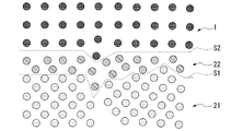
- FIG. 4 is a cross-sectional view of a characteristic portion of the magnetoresistive sensor 100 according to the first embodiment.
- FIG. 4 is an enlarged view of the vicinity of the interface between the first layer 21, the second layer 22, and the first ferromagnetic layer 1.
- the atoms constituting each layer are illustrated by " ⁇ (circle)".
- the first layer 21 has crystallinity. Unless the crystal growth is completely homogeneous, grain boundaries and the like occur, and the interface S1 between the first layer 21 and the second layer 22 becomes uneven. Since the first layer 21 is usually formed by sputtering or the like, it is difficult to make the crystal growth completely homogeneous.
- the second layer 22 is formed on the first layer 21.
- the second layer 22 is amorphous and is formed so as to fill the unevenness of the interface S1. As a result, the interface S2 between the first ferromagnetic layer 1 and the second layer 22 becomes flatter than the interface S1 between the first layer 21 and the second layer 22.
- the first layer 21 contains any one of a metal, an alloy, an intermetal compound, a metal boulder, a metal carbide, a metal siliceate, and a metal phosphate having a function of generating a spin current by the spin Hall effect when an electric current flows. ..
- the first layer 21 contains, for example, a non-magnetic heavy metal as a main component.
- Heavy metal means a metal having a specific density of yttrium (Y) or higher.
- the non-magnetic heavy metal is, for example, a non-magnetic metal having a d-electron or an f-electron in the outermost shell and having an atomic number of 39 or more and a large atomic number.
- the first layer 21 is composed of, for example, Hf, Ta, and W.
- Non-magnetic heavy metals have stronger spin-orbit interactions than other metals. The spin Hall effect is caused by the spin-orbit interaction, and spins are likely to be unevenly distributed in the first layer 21, and spin current JS is likely to occur.
- the first layer 21 may contain a magnetic metal.
- the magnetic metal is a ferromagnetic metal or an antiferromagnetic metal.
- a small amount of magnetic metal contained in the non-magnetic material becomes a scattering factor for spin.
- the trace amount is, for example, 3% or less of the total molar ratio of the elements constituting the first layer 21.
- the first layer 21 may include a topological insulator.
- a topological insulator is a substance in which the inside of the substance is an insulator or a high resistance substance, but a metallic state in which spin polarization occurs on the surface thereof.
- an internal magnetic field is generated by spin-orbit interaction.
- Topological insulators develop a new topological phase due to the effect of spin-orbit interaction even in the absence of an external magnetic field.
- Topological insulators can generate pure spin currents with high efficiency due to strong spin-orbit interaction and breaking of inversion symmetry at the edges.
- Topological insulators include, for example, SnTe, Bi 1.5 Sb 0.5 Te 1.7 Se 1.3 , TlBiSe 2 , Bi 2 Te 3 , Bi 1-x Sb x , (Bi 1-x Sb x ) 2 .
- Te 3 Te 3 .
- Topological insulators can generate spin currents with high efficiency.
- the electrical resistance of the first layer 21 may be lower than the electrical resistance of the second layer 22, which will be described in detail later.
- the electric resistance of the first layer 21 may be 2/3 times or less or 1/2 times or less the electric resistance of the second layer 22.
- the second layer 22 may be any material having conductivity.
- the second layer 22 contains, for example, at least one element of Ta, W, Ti, and Ag. These metal elements do not easily grow grains and easily form a flat film. Further, these elements have a strong spin-orbit interaction, and spin can be efficiently injected from the second layer 22 into the first ferromagnetic layer 1. Further, the second layer 22 may contain at least one element of, for example, Ag, Cu, Mg, and Al. These elements have a long spin diffusion length, and spins are less likely to dissipate in the second layer 22.
- the second layer 22 may contain at least one element of Fe, Co, and Mn, and may contain any element of B or C. Since the second layer 22 contains the same elements as the first ferromagnetic layer 1, a strong spin-orbit interaction is generated in the second layer 22, and a pure spin current can be generated with high efficiency.
- the second layer 22 may contain a nitride containing at least one element selected from the group consisting of Ti, V, Cr, Zr, Nb, Mo, Ta, and W.
- a nitride containing the elements contained in this group it functions not only as a spin conduction layer but also as a spin generation layer. That is, when a current flows in the in-plane direction of the second layer 22, a large spin-orbit torque is generated due to a large spin Hall effect.
- Nitridees containing elements contained in this group have lower electrical resistance than heavy metals and are excellent in conductivity. Therefore, when the second layer 22 containing these nitrides is used, the electric resistance can be lowered while maintaining the spin generation efficiency of the wiring layer 20.
- the film thickness of the first layer 21 is, for example, 10 nm or less, preferably 6 nm or less.
- the film thickness of the first layer 21 is, for example, 1 nm or more. When the film thickness of the first layer 21 is sufficiently thin, the current density of the current flowing in the wiring layer 20 can be increased.
- the film thickness of the second layer 22 is, for example, 4 nm or less.
- the film thickness of the second layer 22 is, for example, one atomic layer or more and 1 nm or more.
- the spin generated in the first layer 21 can be efficiently injected into the first ferromagnetic layer 1.
- the magnetoresistive sensor 100 is formed by a laminating step of each layer and a processing step of processing a part of each layer into a predetermined shape.
- a sputtering method, a chemical vapor deposition (CVD) method, an electron beam vapor deposition method (EB vapor deposition method), an atomic laser deposit method, or the like can be used for the lamination of each layer.
- CVD chemical vapor deposition
- EB vapor deposition method electron beam vapor deposition method
- atomic laser deposit method or the like.
- the processing of each layer can be performed by using photolithography, etching or the like.
- the conductive layer to be the first layer 21 and the conductive layer to be the second layer 22 are laminated in order on the insulator In and the electrodes E2 and E3.
- the laminated surface of the insulator In and the electrodes E2 and E3 is flattened by, for example, chemical mechanical polishing (CMP).
- CMP chemical mechanical polishing
- the degree of vacuum is increased or the film forming power is lowered as compared with the case where the first layer 21 is formed.
- the degree of vacuum may be increased and the film forming power may be lowered as compared with the case of forming the first layer 21.
- the degree of vacuum is lowered or the film forming power is increased, crystal growth proceeds while grain growth occurs, and particulate crystals are likely to be formed.
- the degree of vacuum is increased and the film forming power is decreased, the film growth becomes slow and the flatness of the interface S2 is enhanced.
- a ferromagnetic layer, a non-magnetic layer, and a ferromagnetic layer are formed on the second layer 22 in order. Then, by processing these into a predetermined shape, the first ferromagnetic layer 1, the non-magnetic layer 3, and the second ferromagnetic layer 2 are formed, and the laminated body 10 is obtained. Then, by forming the electrode E1 on the laminated body 10, the magnetoresistive effect element 100 can be obtained.
- the magnetoresistive sensor 100 has a write operation and a read operation.
- the operation of writing data to the magnetoresistive effect element 100 will be described. First, the first switching element Sw1 and the second switching element Sw2 connected to the magnetoresistive effect element 100 to which data is to be written are turned ON. When the first switching element Sw1 and the second switching element Sw2 are turned on, a current flows through the wiring layer 20.
- the first spin is injected into the first ferromagnetic layer 1 due to the spin Hall effect.
- the magnetization of the first ferromagnetic layer 1 is reversed by receiving the spin-orbit torque generated by the injection of the first spin.
- the relative angle with the magnetization of the second ferromagnetic layer 2 changes, and the resistance value of the laminated body 10 changes.
- the magnetoresistive effect element 100 stores data based on the resistance value of the laminated body 10. Therefore, the data writing to the magnetoresistive sensor 100 is completed by the above procedure.
- the third switching element Sw3 and the second switching element Sw2 connected to the magnetoresistive effect element 100 for which data is to be read are turned ON.
- a read current flows in the z direction of the laminated body 10.
- the resistance value of the laminated body 10 differs depending on whether the magnetization of the first ferromagnetic layer 1 and the magnetization of the second ferromagnetic layer 2 are parallel or antiparallel.
- the resistance value of the magnetic resistance effect element 100 becomes low, and the magnetization of the first ferromagnetic layer 1 and the second ferromagnetic layer 2 are parallel.
- the resistance value of the magnetic resistance effect element 100 becomes high.
- the resistance value of the magnetoresistive element 100 is output as a potential difference according to Ohm's law. Therefore, the data reading from the magnetoresistive effect element 100 is completed by the above procedure.
- the magnetoresistive sensor 100 has the second layer 22 so that the interface S2 is flattened.
- the critical current density that reverses the magnetization of the first ferromagnetic layer 1 is strongly influenced by the interface S2. This is because the spin injected into the first ferromagnetic layer 1 is affected by the Rashba effect at the interface and the like.
- the interface S2 is flat, for example, the variation in the critical current density in the element and the variation between the elements can be suppressed.
- the variation in the element is that there is a place where the magnetization is likely to be locally reversed in one magnetoresistive element 100.
- the variation between elements is that the easiness of magnetization reversal of each of the plurality of magnetoresistive elements 100 varies. When the variation in the critical current density becomes small, it is not necessary to design a high critical current density required for reliable writing, and the power consumption of the magnetoresistive effect element 100 can be reduced.
- FIG. 5 is a cross-sectional view of the magnetoresistive effect element 101 according to the first modification.
- FIG. 5 is a cross section of the magnetoresistive sensor 101 cut along the xz plane.
- the magnetoresistive effect element 101 shown in FIG. 5 differs from the magnetoresistive element 100 in the positional relationship of the components.
- the laminated body 10 is on the substrate Sub side of the wiring layer 20.
- the second ferromagnetic layer 2 which is a magnetization fixing layer, is located near the substrate Sub. This configuration is called a bottom pin structure.
- the bottom pin structure has higher magnetization stability of each layer than the top pin structure.
- the wiring layer 20 has a second layer 22 and a first layer 21 in order from the side closer to the laminated body 10.
- the first layer 21 is on the second layer 22.
- the length of the second layer 22 in the x direction is longer than the length of the first layer 21 in the x direction.
- the second layer 22 is between the first layer 21 and the first ferromagnetic layer 1.
- the magnetoresistive effect element 101 according to the first modification has the same effect as the magnetoresistive effect element 100 according to the first embodiment.
- the integrated device according to the first embodiment can be used for, for example, a magnetic memory or the like.
- the integrated device according to the second embodiment is different from the integrated device according to the first embodiment in that it has a magnetization rotating element 110 instead of the magnetoresistive element 100.
- Other configurations are the same as those of the integration device 200 according to the first embodiment, and the description thereof will be omitted.
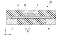
- FIG. 6 is a cross-sectional view of the magnetization rotating element 110 according to the second embodiment.
- FIG. 6 is a cross section of the magnetization rotating element 110 cut in the xz plane.
- the magnetization rotating element 110 is different from the magnetoresistive element 100 according to the first embodiment in that it does not have the non-magnetic layer 3 and the second ferromagnetic layer 2.
- Other configurations are the same as those of the magnetoresistive sensor 100 according to the first embodiment.
- the magnetization rotating element 110 is an example of a magnetic element.
- the magnetizing rotating element 110 incidents light on the first ferromagnetic layer 1 and evaluates the light reflected by the first ferromagnetic layer 1.
- the deflection state of the reflected light changes.
- the magnetization rotating element 110 can be used, for example, as an optical element of, for example, an image display device that utilizes the difference in the deflection state of light.
- the magnetization rotating element 110 can be used alone as an anisotropic magnetic sensor, an optical element utilizing the magnetic Faraday effect, and the like.
- the magnetization rotating element 110 according to the second embodiment only removes the non-magnetic layer 3 and the second ferromagnetic layer 2, and can obtain the same effect as the magnetoresistive effect element 100 according to the first embodiment.
- FIG. 7 is a cross-sectional view of the domain wall moving element 120 according to the third embodiment.
- FIG. 7 is a cross section of the domain wall moving element cut in the xz plane.
- the domain wall moving element 120 has a laminated body 30, a wiring layer 40, a first magnetization fixing layer 50, and a second magnetization fixing layer 60.
- the domain wall moving element 120 is an example of a magnetic element.
- the domain wall moving element 120 is an element whose resistance value changes due to the movement of the domain wall DW.
- the laminated body 30 has a first ferromagnetic layer 31, a second ferromagnetic layer 32, and a non-magnetic layer 33.
- the first ferromagnetic layer 31 contains a ferromagnet.
- the magnetic material constituting the first ferromagnetic layer 31 is a metal selected from the group consisting of Cr, Mn, Co, Fe and Ni, an alloy containing one or more of these metals, these metals and B, C, and An alloy or the like containing at least one element of N can be used. Specific examples thereof include Co-Fe, Co-Fe-B, and Ni-Fe.
- the first ferromagnetic layer 31 is a layer capable of magnetically recording information by changing the internal magnetic state.
- the first ferromagnetic layer 31 has a first region A1 and a second region A2 in which the magnetization is fixed, and a third region A3 in which the domain wall DW can move.
- the first region A1 is a region that overlaps with the first magnetization fixed layer 50 in the z direction.
- the magnetization MA1 of the first region A1 is fixed by the first magnetization fixing layer 50.
- the second region A2 is a region that overlaps with the second magnetization fixed layer 60 in the z direction.
- the magnetization MA2 of the second region A2 is fixed by the second magnetization fixing layer 60.
- the orientation direction of the magnetization MA1 in the first region A1 is different from the orientation direction of the magnetization MA2 in the second region A2 .
- the third domain A3 has a first magnetic domain A3a and a second magnetic domain A3b inside.
- the magnetization MA3a of the first magnetic domain A3a and the magnetization MA3b of the second magnetic domain A3b are oriented in opposite directions, for example.
- the boundary between the first magnetic domain A3a and the second magnetic domain A3b is the domain wall DW.
- the first ferromagnetic layer 1 can have a domain wall DW inside.
- the domain wall moving element 120 can record data in multiple values or continuously depending on the position of the domain wall DW.
- the data recorded in the first ferromagnetic layer 31 is read out as a change in the resistance value of the domain wall moving element 120 when a read-out current is applied.
- the domain wall DW moves by passing a write current in the x direction of the first ferromagnetic layer 31 or by applying an external magnetic field. For example, when a write current (for example, a current pulse) is applied in the + x direction of the first ferromagnetic layer 31, electrons flow in the ⁇ x direction opposite to the current, so that the domain wall DW moves in the ⁇ x direction.
- a current flows from the first magnetic domain A3a to the second magnetic domain A3b, the spin-polarized electrons in the second magnetic domain A3b reverse the magnetization of the first magnetic domain A3a.
- the magnetic domain wall DW moves in the ⁇ x direction due to the magnetization reversal of the first magnetic domain A3a magnetization.
- Each of the second ferromagnetic layer 32 and the non-magnetic layer 33 is the same as the second ferromagnetic layer 2 and the non-magnetic layer 3 according to the first embodiment.
- the wiring layer 40 has a first layer 41 and a second layer 42.
- the wiring layer 40 is in contact with the first ferromagnetic layer 31, and is sandwiched between the first magnetization fixing layer 50 and the second magnetization fixing layer 60 in the x direction.
- Each of the first layer 41 and the second layer 42 is the same as the first layer 21 and the second layer 22 according to the first embodiment.
- the wiring layer 40 generates a spin current by the spin Hall effect when a current flows, and injects spin into the first ferromagnetic layer 1.
- the wiring layer 40 for example, applies spin-orbit torque (SOT) to the magnetization of the first ferromagnetic layer 1.
- SOT spin-orbit torque
- the spin-orbit torque (SOT) generated by the spin injected from the wiring layer 40 assists the movement of the domain wall DW.
- the domain wall DW of the first ferromagnetic layer 1 receives spin-orbit torque (SOT) and becomes easy to move.
- the first magnetization fixed layer 50 and the second magnetization fixed layer 60 are in contact with the first ferromagnetic layer.
- the first magnetization fixed layer 50 and the second magnetization fixed layer 60 are separated from each other in the x direction.
- the first magnetization fixing layer 50 fixes the magnetization of the first region A1.
- the second magnetization fixing layer 60 fixes the magnetization of the second region A2.
- each of the first magnetization fixed layer 50 and the second magnetization fixed layer 60 when viewed from the z direction is, for example, a rectangle.
- the shapes of the first magnetization fixed layer 50 and the second magnetization fixed layer 60 as viewed from the z direction may be, for example, circular, elliptical, oval, or the like.
- the first magnetization fixed layer 50 and the second magnetization fixed layer 60 include, for example, a ferromagnet.
- the first magnetization fixed layer 50 has a ferromagnetic layers 51 and 53 and a spacer layer 52.
- the spacer layer 52 is located between the ferromagnetic layer 51 and the ferromagnetic layer 53.
- the second magnetization fixing layer 60 has a ferromagnetic layers 61 and 63 and a spacer layer 62.
- the spacer layer 62 is located between the ferromagnetic layer 61 and the ferromagnetic layer 63.
- the same material as the second ferromagnetic layer 2 can be used for the ferromagnetic layers 51, 53, 61, 63.
- the spacer layers 52 and 62 are non-magnetic materials.
- the spacer layers 52 and 62 are, for example, Ru, Ir, and Rh.
- the ferromagnetic layer 51 and the ferromagnetic layer 53, and the ferromagnetic layer 61 and the ferromagnetic layer 63 are magnetically coupled in an antiferromagnetic manner, respectively.
- first magnetization fixed layer 50 and the second magnetization fixed layer 60 are not limited to ferromagnets.
- the current of the current flowing through the first ferromagnetic layer 1 in the region overlapping the first magnetized fixed layer 50 or the second magnetized fixed layer 60 limits the movement of the magnetic wall DW and fixes the magnetization of the first region A1 and the second region A2.
- the domain wall moving element 120 has the second layer 42, so that the interface between the wiring layer 20 and the first ferromagnetic layer 1 is flattened. As a result, the variation in the amount of spin injected from the wiring layer 40 into the first ferromagnetic layer 1 becomes small. Further, the unevenness of the surface is one of the factors (pinning sites) that hinder the movement of the domain wall DW, but the flattening of the interface makes the movement of the domain wall DW smooth. Therefore, the domain wall moving element 120 can be driven with low power consumption.
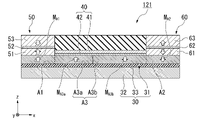
- FIG. 8 is a cross-sectional view of the domain wall moving element 121 according to the second modification.
- FIG. 8 is a cross section of the domain wall moving element 121 cut in the xz plane.
- the domain wall moving element 121 shown in FIG. 8 is different from the domain wall moving element 120 in the positional relationship of the components.
- the laminated body 30 is on the substrate Sub side of the wiring layer 40.
- the second ferromagnetic layer 32 which is a magnetization fixing layer, is located near the substrate Sub. This configuration is called a bottom pin structure.
- the bottom pin structure has higher magnetization stability of each layer than the top pin structure.
- the wiring layer 40 has a second layer 42 and a first layer 41 in order from the side closer to the laminated body 30.
- the first layer 41 is on the second layer 42.
- the length of the second layer 42 in the x direction is longer than the length of the first layer 41 in the x direction.
- the second layer 42 is between the first layer 41 and the first ferromagnetic layer 31.
- the domain wall moving element 121 according to the second modification has the same effect as the domain wall moving element 120 according to the third embodiment.
- the integrated device according to the third embodiment can be applied to an analog element, a spin memory star, and a neuromorphic device.
- a neuromorphic device is an element that imitates the human brain by a neural network.
- Neuromorphic devices artificially mimic the relationship between neurons and synapses in the human brain.
- the neuromorphic device has, for example, hierarchically arranged chips (neurons in the brain) and transmission means (synapses in the brain) connecting them.
- Neuromorphic devices increase the percentage of correct answers to questions by learning by means of communication (synapses). Learning is to find knowledge that can be used in the future from information, and neuromorphic devices weight the input data.
- the product-sum calculation can be performed by arranging the magnetoresistive element or the magnetization rotating element in an array. For example, when a current is passed through the readout path of the magnetoresistive sensor, the product of the input current and the resistance of the magnetoresistive sensor is output, and the product calculation is performed. When a plurality of magnetoresistive elements are connected by a common wiring, the product calculation is added by the common wiring and a sum calculation is performed. Therefore, the magnetic recording array according to the third embodiment can be applied to a neuromorphic device as a product-sum calculator.
Landscapes
- Engineering & Computer Science (AREA)
- Chemical & Material Sciences (AREA)
- Power Engineering (AREA)
- Crystallography & Structural Chemistry (AREA)
- Manufacturing & Machinery (AREA)
- Materials Engineering (AREA)
- Hall/Mr Elements (AREA)
- Mram Or Spin Memory Techniques (AREA)
- Magnetic Heads (AREA)
- Thin Magnetic Films (AREA)
Abstract
本実施形態にかかる磁気素子は、配線層と、前記配線層に接する第1強磁性層と、を備え、前記配線層は、結晶質の第1層と、前記第1強磁性層と前記第1層との間にあり、アモルファスの第2層とを備える。
Description
本発明は、磁気素子及び集積装置に関する。
本願は、2020年10月2日に、日本に出願された特願2020-167660号に基づき優先権を主張し、その内容をここに援用する。
本願は、2020年10月2日に、日本に出願された特願2020-167660号に基づき優先権を主張し、その内容をここに援用する。
強磁性層と非磁性層の多層膜からなる巨大磁気抵抗(GMR)素子、及び、非磁性層に絶縁層(トンネルバリア層、バリア層)を用いたトンネル磁気抵抗(TMR)素子は、磁気抵抗効果素子として知られている。磁気抵抗効果素子は、磁気センサ、高周波部品、磁気ヘッド及び不揮発性ランダムアクセスメモリ(MRAM)への応用が可能である。
MRAMは、磁気抵抗効果素子が集積された記憶素子である。MRAMは、磁気抵抗効果素子における非磁性層を挟む二つの強磁性層の互いの磁化の向きが変化すると、磁気抵抗効果素子の抵抗が変化するという特性を利用してデータを読み書きする。
例えば、特許文献1には、スピン軌道トルク(SOT)を利用して磁気抵抗効果素子の抵抗を変化させる方法が記載されている。SOTは、スピン軌道相互作用によって生じたスピン流又は異種材料の界面におけるラシュバ効果により誘起される。磁気抵抗効果素子内にSOTを誘起するための電流は、磁気抵抗効果素子の積層方向と交差する方向に流れる。磁気抵抗効果素子の積層方向に電流を流す必要がなく、磁気抵抗効果素子の長寿命化が期待されている。
スピン軌道トルクを用いた磁気抵抗効果素子は、強磁性層の磁化を反転させることでデータを記録する。強磁性層の磁化は、印加された電流の電流密度が臨界電流密度以上の場合に反転する。磁化反転に要する臨界電流密度が大きくなると、素子の消費電力が増大する。
本発明は上記事情に鑑みてなされたものであり、消費電力が小さい磁気素子及び集積装置を提供することを目的とする。
本発明は、上記課題を解決するため、以下の手段を提供する。
(1)第1の態様にかかる磁気素子は、配線層と、前記配線層に接する第1強磁性層と、を備え、前記配線層は、結晶質の第1層と、前記第1強磁性層と前記第1層との間にあり、アモルファスの第2層とを備える。
(2)上記態様に係る磁気素子において、前記第1層の電気抵抗率は前記第2層の電気抵抗率よりも低くてもよい。
(3)上記態様にかかる磁気素子において、前記第2層は、Ta、W、Ti、Agのうちの少なくとも一つの元素を含んでもよい。
(4)上記態様にかかる磁気素子において、前記第2層は、Fe、Co、Mnのうちの少なくとも一つの元素を含んでもよい。
(5)上記態様にかかる磁気素子において、前記第2層は、B又はCのいずれかの元素を含んでもよい。
(6)上記態様にかかる磁気素子において、前記第2層は、Ti,V,Cr,Zr,Nb,Mo,Ta,Wからなる群から選択された少なくとも一つの元素を含む窒化物を含んでいてもよい。
(7)上記態様にかかる磁気素子において、前記第2層の膜厚は、4nm以下でもよい。
(8)上記態様にかかる磁気素子において、前記第1層の膜厚は、4nm以下でもよい。
(9)上記態様にかかる磁気素子において、前記配線層は、第1方向の長さが他の方向の長さより長く、前記第1層の前記第1方向の長さは、前記第2層の前記第1方向の長さより長くてもよい。
(10)上記態様にかかる磁気素子において、前記配線層は、第1方向の長さが他の方向の長さより長く、前記第2層の前記第1方向の長さは、前記第1層の前記第1方向の長さより長くてもよい。
(11)上記態様にかかる磁気素子は、第2強磁性層と非磁性層とをさらに備え、前記非磁性層は、前記第1強磁性層と前記第2強磁性層とに挟まれてもよい。
(12)上記態様にかかる磁気素子は、第1磁化固定層と第2磁化固定層とをさらに備え、前記第1磁化固定層と前記第2磁化固定層とはそれぞれ、前記第1強磁性層を挟む位置で前記配線層に接し、前記第1強磁性層は、内部に磁壁を有してもよい。
(13)第2の態様にかかる磁気素子は、配線層と、前記配線層に接する第1強磁性層と、を備え、前記配線層は、第1層と、前記第1強磁性層と前記第1層との間にある第2層とを備え、前記第1層は、透過型電子顕微鏡(TEM)を用いてナノ電子回折(NBD)を行った際に、回折パターンが得られ、前記第2層は、透過型電子顕微鏡(TEM)を用いてナノ電子回折(NBD)を行った際に、回折パターンが得られない。
(14)第2の態様にかかる集積装置は、上記態様にかかる磁気素子を複数有する。
本実施形態にかかる磁気抵抗効果素子及び磁気メモリは、消費電力が小さい。
以下、本実施形態について、図を適宜参照しながら詳細に説明する。以下の説明で用いる図面は、特徴をわかりやすくするために便宜上特徴となる部分を拡大して示している場合があり、各構成要素の寸法比率などは実際とは異なっていることがある。以下の説明において例示される材料、寸法等は一例であって、本発明はそれらに限定されるものではなく、本発明の効果を奏する範囲で適宜変更して実施することが可能である。
まず方向について定義する。後述する基板Sub(図2参照)の一面の一方向をx方向、基板Subの一面の一方向のうちx方向と直交する方向をy方向とする。x方向は、配線層20が延びる方向であり、第1方向の一例である。z方向は、x方向及びy方向と直交する方向である。z方向は、積層方向の一例である。以下、+z方向を「上」、-z方向を「下」と表現する場合がある。上下は、必ずしも重力が加わる方向とは一致しない。
本明細書で「x方向に延びる」とは、例えば、x方向、y方向、及びz方向の各寸法のうち最小の寸法よりもx方向の寸法が大きいことを意味する。他の方向に延びる場合も同様である。また本明細書で「接続」とは、物理的に接続される場合に限定されない。例えば、二つの層が物理的に接している場合に限られず、二つの層の間が他の層を間に挟んで接続している場合も「接続」に含まれる。また2つの部材が電気的に接続されている場合も「接続」に含まれる。
「第1実施形態」
図1は、第1実施形態にかかる集積装置200の回路図である。集積装置200は、複数の磁気抵抗効果素子100と、複数の書き込み配線Wpと、複数の共通配線Cmと、複数の読み出し配線Rpと、複数の第1スイッチング素子Sw1と、複数の第2スイッチング素子Sw2と、複数の第3スイッチング素子Sw3とを備える。集積装置200は、例えば、磁気記録アレイ、磁気メモリ等に利用できる。磁気抵抗効果素子100は、磁気素子の一例である。
図1は、第1実施形態にかかる集積装置200の回路図である。集積装置200は、複数の磁気抵抗効果素子100と、複数の書き込み配線Wpと、複数の共通配線Cmと、複数の読み出し配線Rpと、複数の第1スイッチング素子Sw1と、複数の第2スイッチング素子Sw2と、複数の第3スイッチング素子Sw3とを備える。集積装置200は、例えば、磁気記録アレイ、磁気メモリ等に利用できる。磁気抵抗効果素子100は、磁気素子の一例である。
書き込み配線Wpのそれぞれは、電源と1つ以上の磁気抵抗効果素子100とを電気的に接続する。共通配線Cmのそれぞれは、データの書き込み時及び読み出し時の両方で用いられる配線である。共通配線Cmは、基準電位と1つ以上の磁気抵抗効果素子100とを電気的に接続する。基準電位は、例えば、グラウンドである。共通配線Cmは、複数の磁気抵抗効果素子100のそれぞれに設けられてもよいし、複数の磁気抵抗効果素子100に亘って設けられてもよい。読み出し配線Rpのそれぞれは、電源と1つ以上の磁気抵抗効果素子100とを電気的に接続する。電源は、使用時に集積装置200に接続される。
第1スイッチング素子Sw1、第2スイッチング素子Sw2、第3スイッチング素子Sw3は、例えば、一つの磁気抵抗効果素子100にそれぞれ接続されている。第1スイッチング素子Sw1は、磁気抵抗効果素子100と書き込み配線Wpとの間に接続されている。第2スイッチング素子Sw2は、磁気抵抗効果素子100と共通配線Cmとの間に接続されている。第3スイッチング素子Sw3は、磁気抵抗効果素子100と読み出し配線Rpとの間に接続されている。
所定の第1スイッチング素子Sw1及び第2スイッチング素子Sw2をONにすると、所定の磁気抵抗効果素子100に接続された書き込み配線Wpと共通配線Cmとの間に書き込み電流が流れる。所定の第2スイッチング素子Sw2及び第3スイッチング素子Sw3をONにすると、所定の磁気抵抗効果素子100に接続された共通配線Cmと読み出し配線Rpとの間に読み出し電流が流れる。
第1スイッチング素子Sw1、第2スイッチング素子Sw2及び第3スイッチング素子Sw3は、電流の流れを制御する素子である。第1スイッチング素子Sw1、第2スイッチング素子Sw2及び第3スイッチング素子Sw3は、例えば、トランジスタ、オボニック閾値スイッチ(OTS:Ovonic Threshold Switch)のように結晶層の相変化を利用した素子、金属絶縁体転移(MIT)スイッチのようにバンド構造の変化を利用した素子、ツェナーダイオード及びアバランシェダイオードのように降伏電圧を利用した素子、原子位置の変化に伴い伝導性が変化する素子である。
第1スイッチング素子Sw1、第2スイッチング素子Sw2、第3スイッチング素子Sw3のいずれかは、同じ配線に接続された磁気抵抗効果素子100で、共用してもよい。例えば、第1スイッチング素子Sw1を共有する場合は、書き込み配線Wpの上流に一つの第1スイッチング素子Sw1を設ける。例えば、第2スイッチング素子Sw2を共有する場合は、共通配線Cmの上流に一つの第2スイッチング素子Sw2を設ける。例えば、第3スイッチング素子Sw3を共有する場合は、読み出し配線Rpの上流に一つの第3スイッチング素子Sw3を設ける。
図2は、第1実施形態に係る集積装置200の断面図である。図2は、磁気抵抗効果素子100を後述する配線層20のy方向の幅の中心を通るxz平面で切断した断面である。
図2に示す第1スイッチング素子Sw1及び第2スイッチング素子Sw2は、トランジスタTrである。第3スイッチング素子Sw3は、電極E1と電気的に接続され、例えば、図2のy方向に位置する。トランジスタTrは、例えば電界効果型のトランジスタであり、ゲート電極Gとゲート絶縁膜GIと基板Subに形成されたソースS及びドレインDとを有する。基板Subは、例えば、半導体基板である。
トランジスタTrと磁気抵抗効果素子100とは、配線w及び電極E2、E3を介して、電気的に接続されている。またトランジスタTrと書き込み配線Wp又は共通配線Cmとは、配線wで接続されている。配線wは、例えば、接続配線、ビア配線、層間配線と言われることがある。配線w及び電極E2、E3は、導電性を有する材料を含む。配線wは、例えば、z方向に延びる。
磁気抵抗効果素子100及びトランジスタTrの周囲は、絶縁体Inで覆われている。絶縁体Inは、多層配線の配線間や素子間を絶縁する絶縁体である。絶縁体Inは、例えば、酸化シリコン(SiOx)、窒化シリコン(SiNx)、炭化シリコン(SiC)、窒化クロム、炭窒化シリコン(SiCN)、酸窒化シリコン(SiON)、酸化アルミニウム(Al2O3)、酸化ジルコニウム(ZrOx)等である。
図3は、第1実施形態に係る磁気抵抗効果素子100の断面図である。図3は、磁気抵抗効果素子100をxz平面で切断した断面である。
磁気抵抗効果素子100は、例えば、積層体10と配線層20とを有する。磁気抵抗効果素子100は、スピン軌道トルク(SOT)を利用した磁性素子であり、スピン軌道トルク型磁気抵抗効果素子、スピン注入型磁気抵抗効果素子、スピン流磁気抵抗効果素子と言われる場合がある。
積層体10は、基板Subに近い側から順に第1強磁性層1、非磁性層3、第2強磁性層2を有する。積層体10は、配線層20上に積層されている。積層体10は、z方向に、配線層20と電極E1とに挟まれる。積層体10は、柱状体である。積層体10は、上面から下面に向かって徐々に拡幅している。積層体10のz方向からの平面視形状は、例えば、円形、楕円形、四角形である。
第1強磁性層1及び第2強磁性層2は、強磁性体を含む。強磁性体は、例えば、Cr、Mn、Co、Fe及びNiからなる群から選択される金属、これらの金属を1種以上含む合金、これらの金属とB、C、及びNの少なくとも1種以上の元素とが含まれる合金等である。強磁性体は、例えば、Co-Fe、Co-Fe-B、Ni-Fe、Co-Ho合金、Sm-Fe合金、Fe-Pt合金、Co-Pt合金、CoCrPt合金である。
第1強磁性層1及び第2強磁性層2は、ホイスラー合金を含んでもよい。ホイスラー合金は、XYZまたはX2YZの化学組成をもつ金属間化合物を含む。Xは周期表上でCo、Fe、Ni、あるいはCu族の遷移金属元素または貴金属元素であり、YはMn、V、CrあるいはTi族の遷移金属又はXの元素種であり、ZはIII族からV族の典型元素である。ホイスラー合金は、例えば、Co2FeSi、Co2FeGe、Co2FeGa、Co2MnSi、Co2Mn1-aFeaAlbSi1-b、Co2FeGe1-cGac等である。ホイスラー合金は高いスピン分極率を有する。
第1強磁性層1及び第2強磁性層2は、例えば、磁化容易軸がz方向である垂直磁化膜である。第1強磁性層1及び第2強磁性層2は、例えば、磁化容易軸がxy面内のいずれかの方向に配向した面内磁化膜でもよい。
第2強磁性層2の磁化は、所定の外力が印加された際に第1強磁性層1の磁化よりも配向方向が変化しにくい。第2強磁性層2は磁化固定層、磁化参照層と言われ、第1強磁性層1は磁化自由層と言われる。積層体10は、磁化固定層が基板Subから遠い側にあるトップピン構造である。積層体10は、非磁性層3を挟む第1強磁性層1の磁化と第2強磁性層2の磁化との相対角の違いに応じて抵抗値が変化する。
非磁性層3は、非磁性体からなる。非磁性層3が絶縁体の場合(トンネルバリア層である場合)、その材料としては、例えば、Al2O3、SiO2、MgO、及び、MgAl2O4等を用いることができる。また、これらの他にも、Al、Si、Mgの一部が、Zn、Be等に置換された材料等も用いることができる。これらの中でも、MgOやMgAl2O4はコヒーレントトンネルが実現できる材料であるため、スピンを効率よく注入できる。非磁性層3が金属の場合、その材料としては、Cu、Au、Ag等を用いることができる。さらに、非磁性層3が半導体の場合、その材料としては、Si、Ge、CuInSe2、CuGaSe2、Cu(In,Ga)Se2等を用いることができる。
積層体10は、第1強磁性層1、非磁性層3、第2強磁性層2以外の層を有してもよい。例えば、第2強磁性層2の非磁性層3と反対側の面に、スペーサ層と第3強磁性層とを有してもよい。第2強磁性層2と第3強磁性層とが磁気的にカップリングすることで、第2強磁性層2の磁化安定性が高まる。第2強磁性層、スペーサ層、第3強磁性層は、シンセティック反強磁性構造(SAF構造)である。第3強磁性層は、第1強磁性層1と同様の材料を用いることができる。第3強磁性層は、例えば、Co/Ni、Co/Ptなどの磁性膜のみ、あるいは、磁性膜と非磁性膜の多層膜によって形成される垂直磁化膜であることが好ましい。スペーサ層は、例えば、Ru、Ir、Rhからなる群から選択される少なくとも一つを含む。また第1強磁性層1の下面に下地層を有してもよい。下地層は、積層体10を構成する各層の結晶性を高める。
配線層20は、第1強磁性層1に接する。配線層20は、電流が流れる際のスピンホール効果によってスピン流を発生させ、第1強磁性層1にスピンを注入する。配線層20は、スピン軌道トルク配線と称される。配線層20は、例えば、第1強磁性層1の磁化を反転できるだけのスピン軌道トルク(SOT)を第1強磁性層1の磁化に与える。配線層20を流れる電流の電流密度が臨界電流密度以上の場合に、第1強磁性層1の磁化が反転する。
スピンホール効果は、電流を流した場合にスピン軌道相互作用に基づき、電流の流れる方向と直交する方向にスピン流が誘起される現象である。スピンホール効果は、運動(移動)する電荷(電子)が運動(移動)方向を曲げられる点で、通常のホール効果と共通する。通常のホール効果は、磁場中で運動する荷電粒子の運動方向がローレンツ力によって曲げられる。これに対し、スピンホール効果は磁場が存在しなくても、電子が移動するだけ(電流が流れるだけ)でスピンの移動方向が曲げられる。
例えば、配線層20に電流が流れると、一方向に配向した第1スピンと、第1スピンと反対方向に配向した第2スピンとが、それぞれ電流の流れる方向と直交する方向にスピンホール効果によって曲げられる。例えば、+y方向に配向した第1スピンが+z方向に向かい、-y方向に配向した第2スピンが-z方向に向かう。
非磁性体(強磁性体ではない材料)は、スピンホール効果により生じる第1スピンの電子数と第2スピンの電子数とが等しい。すなわち、+z方向に向かう第1スピンの電子数と-z方向に向かう第2スピンの電子数とは等しい。第1スピンと第2スピンは、スピンの偏在を解消する方向に流れる。第1スピン及び第2スピンのz方向への移動において、電荷の流れは互いに相殺されるため、電流量はゼロとなる。電流を伴わないスピン流は特に純スピン流と呼ばれる。
第1スピンの電子の流れをJ↑、第2スピンの電子の流れをJ↓、スピン流をJSと表すと、スピン流JSは、JS=J↑-J↓で定義される。スピン流JSは、z方向に生じる。
配線層20は、例えば、x方向及びy方向の側面がz方向に対して傾斜している。配線層20の上面は、例えば、下面より面積が狭い。配線層20の上面のx方向の幅は、例えば、下面のx方向の幅より狭い。
配線層20は、第1層21と第2層22とを有する。第1層21のx方向の長さは、第2層22のx方向の長さより長い。第2層22は、第1層21と第1強磁性層1との間にある。
第1層21は、結晶質である。すなわち、第1層21は、結晶質の材料で構成されている。第1層21は、結晶性を有すれば、単結晶でも結晶粒が集合した多結晶でもよい。「結晶性を有する」か否かは、例えば、透過型電子顕微鏡(TEM)を用いてナノ電子回折(NBD)を行った際に、回折パターンを確認できるか否かで判断できる。回折パターンは、薄片化した薄片試料に1nm径程度に絞った電子線を照射し、電子線を透過回折して得られる電子像である。回折パターンは、結晶格子をフーリエ変換したものであり、有効的な格子定数の変化や結晶対称性の変化を観察している。
第2層22は、アモルファスである。すなわち、第2層22は、アモルファス材料で構成されている。第2層22は、透過型電子顕微鏡(TEM)を用いてナノ電子回折(NBD)を行った際に、回折パターンが確認できない。回折パターンが確認できないとは、回折スポットが規則的に配列していないことを意味する。
図4は、第1実施形態にかかる磁気抵抗効果素子100の特徴部分の断面図である。図4は、第1層21、第2層22及び第1強磁性層1の界面の近傍を拡大した図である。図4では、各層を構成する原子を「〇(円)」で図示している。
第1層21は、結晶性を有する。結晶成長が完全に均質でない限り、結晶粒界等が生じ、第1層21と第2層22との界面S1は凹凸になる。第1層21は、通常、スパッタリング等で成膜されるため、結晶成長を完全に均質にすることは難しい。
第2層22は、第1層21上に成膜される。第2層22は、アモルファスであり、界面S1の凹凸を埋めるように成膜される。その結果、第1強磁性層1と第2層22との界面S2は、第1層21と第2層22との界面S1より平坦になる。
第1層21は、電流が流れる際のスピンホール効果によってスピン流を発生させる機能を有する金属、合金、金属間化合物、金属硼化物、金属炭化物、金属珪化物、金属燐化物のいずれかを含む。
第1層21は、例えば、主成分として非磁性の重金属を含む。重金属は、イットリウム(Y)以上の比重を有する金属を意味する。非磁性の重金属は、例えば、最外殻にd電子又はf電子を有する原子番号39以上の原子番号が大きい非磁性金属である。第1層21は、例えば、Hf、Ta、Wからなる。非磁性の重金属は、その他の金属よりスピン軌道相互作用が強く生じる。スピンホール効果はスピン軌道相互作用により生じ、第1層21内にスピンが偏在しやすく、スピン流JSが発生しやすくなる。
第1層21は、磁性金属を含んでもよい。磁性金属は、強磁性金属又は反強磁性金属である。非磁性体に含まれる微量な磁性金属は、スピンの散乱因子となる。微量とは、例えば、第1層21を構成する元素の総モル比の3%以下である。スピンが磁性金属により散乱するとスピン軌道相互作用が増強され、電流に対するスピン流の生成効率が高くなる。
第1層21は、トポロジカル絶縁体を含んでもよい。トポロジカル絶縁体は、物質内部が絶縁体又は高抵抗体であるが、その表面にスピン偏極した金属状態が生じている物質である。トポロジカル絶縁体は、スピン軌道相互作用により内部磁場が生じる。トポロジカル絶縁体は、外部磁場が無くてもスピン軌道相互作用の効果で新たなトポロジカル相が発現する。トポロジカル絶縁体は、強いスピン軌道相互作用とエッジにおける反転対称性の破れにより純スピン流を高効率に生成できる。
トポロジカル絶縁体は、例えば、SnTe、Bi1.5Sb0.5Te1.7Se1.3、TlBiSe2、Bi2Te3、Bi1-xSbx、(Bi1-xSbx)2Te3などである。トポロジカル絶縁体は、高効率にスピン流を生成することが可能である。
第1層21の電気抵抗は、詳細を後述する第2層22の電気抵抗よりも低くてもよい。例えば、第1層21の電気抵抗は、第2層22の電気抵抗の2/3倍以下や1/2倍以下であってもよい。配線層20がこのような第1層21および第2層22を備えることで、第1層21に第2層22よりも大きな電流が流れ、大きなジュール熱が発生する。そのため、第1層21から第2層22を介して第1強磁性層1に向かって、積層方向に熱流が形成される。熱とスピンは、互いに影響を及ぼし合うため、熱流によって、配線層20から第1強磁性層1へスピンが注入されやすくなる。すなわち、少ない電流で第1強磁性層1の磁化を反転しやすくできる。
第2層22は、導電性を有する材料であればよい。第2層22は、例えば、Ta、W、Ti、Agのうちの少なくとも一つの元素を含む。これらの金属元素は、粒成長しにくく、平坦に成膜しやすい。またこれらの元素は、スピン軌道相互作用が強く、第2層22からも第1強磁性層1にスピンを効率的に注入できる。また第2層22は、例えば、Ag、Cu、Mg、Alのうちの少なくとも一つの元素を含んでもよい。これらの元素は、スピン拡散長が長く、第2層22でスピンが散逸しにくくなる。
また第2層22は、Fe、Co、Mnのうちの少なくとも一つの元素を含んでもよく、B又はCのいずれかの元素を含んでもよい。第2層22が第1強磁性層1と同様の元素を含むことで、第2層22において強いスピン軌道相互作用を生じ、純スピン流を高効率に生成できる。
また第2層22は、Ti,V,Cr,Zr,Nb,Mo,Ta,Wからなる群から選択された少なくとも一つの元素を含む窒化物を含んでいてもよい。第2層22が、この群に含まれる元素を含む窒化物を含む場合、スピン伝導層としてだけでなく、スピン生成層としても機能する。すなわち、第2層22の面内方向に電流が流れると、大きなスピンホール効果により、大きなスピン軌道トルクを生じさせる。この群に含まれる元素を含む窒化物は、重金属と比べ電気抵抗が低く、導電性に優れる。そのため、これらの窒化物を含む第2層22用いた場合、配線層20のスピン生成効率を維持しながら電気抵抗を下げることができる。
第1層21の膜厚は、例えば、10nm以下であり、好ましくは6nm以下である。第1層21の膜厚は、例えば、1nm以上である。第1層21の膜厚が十分薄いと、配線層20内を流れる電流の電流密度を高めることができる。
第2層22の膜厚は、例えば、4nm以下である。第2層22の膜厚は、例えば、原子1層分以上であり、1nm以上である。第2層22の膜厚が、第2層22のスピン拡散長以下であることで、第1層21で生じたスピンを第1強磁性層1に効率的に注入できる。
次いで、磁気抵抗効果素子100の製造方法について説明する。磁気抵抗効果素子100は、各層の積層工程と、各層の一部を所定の形状に加工する加工工程により形成される。各層の積層は、スパッタリング法、化学気相成長(CVD)法、電子ビーム蒸着法(EB蒸着法)、原子レーザデポジッション法等を用いることができる。各層の加工は、フォトリソグラフィー、エッチング等を用いて行うことができる。
まず絶縁体In、電極E2、E3上に、第1層21となる導電層、第2層22となる導電層を順に積層する。絶縁体In及び電極E2、E3の積層面は、例えば、化学機械研磨(CMP)で平坦化されている。第1層21となる導電層及び第2層22となる導電層を所定の形状に加工することで、第1層21と第2層22とが得られる。
第2層22を成膜する際は、例えば、第1層21を成膜する際より真空度を上げる、又は、成膜パワーを低下させる。第2層22を成膜する際は、例えば、第1層21を成膜する際より真空度を上げ、かつ、成膜パワーを低下させてもよい。真空度を低くするか、或いは成膜パワーを大きくすると、結晶成長が粒成長しながら進み、粒子状の結晶ができやすくなる。反対に、真空度を高め、成膜パワーを下げると、膜成長が緩やかになり、界面S2の平坦性が高まる。
次いで、第2層22上に、強磁性層、非磁性層、強磁性層を順に成膜する。その後、これらを所定の形状に加工することで、第1強磁性層1、非磁性層3、第2強磁性層2となり、積層体10が得られる。その後、積層体10上に電極E1を成膜することで、磁気抵抗効果素子100が得られる。
次いで、磁気抵抗効果素子100の動作について説明する。磁気抵抗効果素子100は、書き込み動作と読出し動作がある。
磁気抵抗効果素子100へのデータの書き込み動作について説明する。まずデータを書き込みたい磁気抵抗効果素子100に接続される第1スイッチング素子Sw1及び第2スイッチング素子Sw2をONにする。第1スイッチング素子Sw1及び第2スイッチング素子Sw2をONにすると、配線層20に電流が流れる。
配線層20に電流が流れると、スピンホール効果により第1スピンが第1強磁性層1に注入される。第1強磁性層1の磁化は、第1スピンが注入されることで生じるスピン軌道トルクを受けて反転する。第1強磁性層1の磁化の向きが変化することで、第2強磁性層2の磁化との相対角が変化し、積層体10の抵抗値が変化する。磁気抵抗効果素子100は、積層体10の抵抗値に基づいてデータを記憶する。したがって、上記手順で磁気抵抗効果素子100へのデータ書き込みが完了する。
磁気抵抗効果素子100からのデータの読出し動作について説明する。まずデータを読み出したい磁気抵抗効果素子100に接続される第3スイッチング素子Sw3及び第2スイッチング素子Sw2をONにする。第3スイッチング素子Sw3及び第2スイッチング素子Sw2をONにすると、積層体10のz方向に読出し電流が流れる。
積層体10の抵抗値は、第1強磁性層1の磁化と第2強磁性層2の磁化とが、平行な場合と反平行な場合とで異なる。第1強磁性層1の磁化と第2強磁性層2の磁化とが平行な場合は、磁気抵抗効果素子100の抵抗値は低くなり、第1強磁性層1の磁化と第2強磁性層2の磁化とが反平行な場合は、磁気抵抗効果素子100の抵抗値は高くなる。磁気抵抗効果素子100の抵抗値は、オームの法則により電位差として出力される。したがって、上記手順で磁気抵抗効果素子100からのデータ読出しが完了する。
第1実施形態にかかる磁気抵抗効果素子100は、第2層22があることで、界面S2が平坦化する。第1強磁性層1の磁化を反転させる臨界電流密度は、界面S2の影響を強く受ける。第1強磁性層1に注入されるスピンは、界面におけるラシュバ効果等の影響を受けるためである。界面S2が平坦であると、例えば、臨界電流密度の素子内バラツキや素子間バラツキを抑制できる。素子内バラツキは、一つの磁気抵抗効果素子100内において局所的に磁化が反転しやすい場所が生じることである。素子間バラツキは、複数の磁気抵抗効果素子100のそれぞれの磁化反転しやすさがばらつくことである。臨界電流密度のバラツキが小さくなると、確実な書き込みを行うために必要な臨界電流密度を高めに設計する必要がなくなり、磁気抵抗効果素子100の消費電力を小さくできる。
(第1変形例)
図5は、第1変形例にかかる磁気抵抗効果素子101の断面図である。図5は、磁気抵抗効果素子101をxz平面で切断した断面である。図5に示す磁気抵抗効果素子101は、構成要素の位置関係が磁気抵抗効果素子100と異なる。
図5は、第1変形例にかかる磁気抵抗効果素子101の断面図である。図5は、磁気抵抗効果素子101をxz平面で切断した断面である。図5に示す磁気抵抗効果素子101は、構成要素の位置関係が磁気抵抗効果素子100と異なる。
磁気抵抗効果素子101は、積層体10が配線層20より基板Sub側にある。積層体10において、磁化固定層である第2強磁性層2が基板Subの近くにある。当該構成は、ボトムピン構造と言われる。ボトムピン構造は、トップピン構造より各層の磁化の安定性が高い。
配線層20は、積層体10に近い側から順に、第2層22、第1層21を有する。第1層21は、第2層22上にある。第2層22のx方向の長さは、第1層21のx方向の長さより長い。第2層22は、第1層21と第1強磁性層1との間にある。
第2層22が第1層21と第1強磁性層1との間にあることで、第1層21と第1強磁性層1との間に平坦な界面が形成される。その結果、第1変形例に係る磁気抵抗効果素子101は、第1実施形態にかかる磁気抵抗効果素子100と同様の効果を奏する。
第1実施形態にかかる集積装置は、例えば、磁気メモリ等に用いることができる。
「第2実施形態」
第2実施形態にかかる集積装置は、磁気抵抗効果素子100に変えて磁化回転素子110を有する点が、第1実施形態にかかる集積装置と異なる。その他の構成は、第1実施形態に係る集積装置200と同様であり、説明を省く。
第2実施形態にかかる集積装置は、磁気抵抗効果素子100に変えて磁化回転素子110を有する点が、第1実施形態にかかる集積装置と異なる。その他の構成は、第1実施形態に係る集積装置200と同様であり、説明を省く。
図6は、第2実施形態にかかる磁化回転素子110の断面図である。図6は、磁化回転素子110をxz平面で切断した断面である。磁化回転素子110は、非磁性層3及び第2強磁性層2を有さない点が、第1実施形態に係る磁気抵抗効果素子100と異なる。その他の構成は、第1実施形態に係る磁気抵抗効果素子100と同様である。
磁化回転素子110は、磁気素子の一例である。磁化回転素子110は、例えば、第1強磁性層1に対して光を入射し、第1強磁性層1で反射した光を評価する。磁気カー効果により磁化の配向方向が変化すると、反射した光の偏向状態が変わる。磁化回転素子110は、例えば、光の偏向状態の違いを利用した例えば映像表示装置等の光学素子として用いることができる。
この他、磁化回転素子110は、単独で、異方性磁気センサ、磁気ファラデー効果を利用した光学素子等としても利用できる。
第2実施形態にかかる磁化回転素子110は、非磁性層3及び第2強磁性層2を除いただけであり、第1実施形態にかかる磁気抵抗効果素子100と同様の効果を得ることができる。
「第3実施形態」
図7は、第3実施形態に係る磁壁移動素子120の断面図である。図7は、磁壁移動素子をxz平面で切断した断面である。
図7は、第3実施形態に係る磁壁移動素子120の断面図である。図7は、磁壁移動素子をxz平面で切断した断面である。
磁壁移動素子120は、積層体30と配線層40と第1磁化固定層50と第2磁化固定層60とを有する。磁壁移動素子120は、磁気素子の一例である。磁壁移動素子120は、磁壁DWの移動により抵抗値が変化する素子である。
積層体30は、第1強磁性層31と第2強磁性層32と非磁性層33とを有する。
第1強磁性層31は、強磁性体を含む。第1強磁性層31を構成する磁性体は、Cr、Mn、Co、Fe及びNiからなる群から選択される金属、これらの金属を1種以上含む合金、これらの金属とB、C、及びNの少なくとも1種以上の元素とが含まれる合金等を用いることができる。具体的には、Co-Fe、Co-Fe-B、Ni-Feが挙げられる。
第1強磁性層31は、内部の磁気的な状態の変化により情報を磁気記録可能な層である。第1強磁性層31は、磁化が固定された第1領域A1及び第2領域A2と、磁壁DWが移動できる第3領域A3とを有する。
第1領域A1は、第1磁化固定層50とz方向に重なる領域である。第1領域A1の磁化MA1は、第1磁化固定層50により固定されている。第2領域A2は、第2磁化固定層60とz方向に重なる領域である。第2領域A2の磁化MA2は、第2磁化固定層60により固定されている。第1領域A1の磁化MA1の配向方向は、第2領域A2の磁化MA2の配向方向と異なる。
第3領域A3は、内部に第1磁区A3aと第2磁区A3bとを有する。第1磁区A3aの磁化MA3aと第2磁区A3bの磁化MA3bとは、例えば、反対方向に配向する。第1磁区A3aと第2磁区A3bとの境界が磁壁DWである。第1強磁性層1は、磁壁DWを内部に有することができる。
磁壁移動素子120は、磁壁DWの位置によって、データを多値又は連続的に記録できる。第1強磁性層31に記録されたデータは、読み出し電流を印加した際に、磁壁移動素子120の抵抗値変化として読み出される。
磁壁DWは、第1強磁性層31のx方向に書き込み電流を流す、又は、外部磁場を印加することによって移動する。例えば、第1強磁性層31の+x方向に書き込み電流(例えば、電流パルス)を印加すると、電子は電流と逆の-x方向に流れるため、磁壁DWは-x方向に移動する。第1磁区A3aから第2磁区A3bに向って電流が流れる場合、第2磁区A3bでスピン偏極した電子は、第1磁区A3aの磁化を磁化反転させる。第1磁区A3a磁化が磁化反転することで、磁壁DWが-x方向に移動する。
第2強磁性層32と非磁性層33のそれぞれは、第1実施形態にかかる第2強磁性層2と非磁性層3と同様である。
配線層40は、第1層41と第2層42とを有する。配線層40は、第1強磁性層31に接し、x方向に第1磁化固定層50と第2磁化固定層60とに挟まれる。第1層41と第2層42のそれぞれは、第1実施形態にかかる第1層21と第2層22と同様である。
配線層40は、電流が流れる際のスピンホール効果によってスピン流を発生させ、第1強磁性層1にスピンを注入する。配線層40は、例えば、第1強磁性層1の磁化にスピン軌道トルク(SOT)を与える。配線層40から注入されたスピンにより生じるスピン軌道トルク(SOT)は、磁壁DWの移動をアシストする。第1強磁性層1の磁壁DWは、スピン軌道トルク(SOT)を受けて動きやすくなる。
第1磁化固定層50及び第2磁化固定層60は、第1強磁性層と接する。第1磁化固定層50と第2磁化固定層60とは、x方向に離間している。第1磁化固定層50は、第1領域A1の磁化を固定する。第2磁化固定層60は、第2領域A2の磁化を固定する。
第1磁化固定層50及び第2磁化固定層60のそれぞれをz方向から見た形状は、例えば、矩形である。第1磁化固定層50及び第2磁化固定層60のそれぞれをz方向から見た形状は、例えば、円形、楕円形、オーバル等でもよい。
第1磁化固定層50及び第2磁化固定層60は、例えば、強磁性体を含む。第1磁化固定層50は、強磁性層51,53とスペーサ層52とを有する。スペーサ層52は、強磁性層51と強磁性層53との間にある。第2磁化固定層60は、強磁性層61,63とスペーサ層62とを有する。スペーサ層62は、強磁性層61と強磁性層63との間にある。
強磁性層51,53,61,63は、第2強磁性層2と同様の材料を用いることができる。スペーサ層52,62は、非磁性体である。スペーサ層52,62は、例えば、Ru、Ir、Rhである。強磁性層51と強磁性層53、及び、強磁性層61と強磁性層63とは、それぞれ反強磁性的に磁気結合している。
また第1磁化固定層50及び第2磁化固定層60は、強磁性体に限られない。第1磁化固定層50及び第2磁化固定層60が強磁性体ではない場合は、第1磁化固定層50又は第2磁化固定層60と重なる領域で第1強磁性層1を流れる電流の電流密度が急激に変化することで、磁壁DWの移動が制限され、第1領域A1及び第2領域A2の磁化が固定される。
第3実施形態にかかる磁壁移動素子120は、第2層42があることで、配線層20と第1強磁性層1との界面が平坦化する。その結果、配線層40から第1強磁性層1に注入されるスピン量のバラツキが小さくなる。また表面の凹凸は、磁壁DWの移動を妨げる要因の一つ(ピニングサイト)であるが、界面が平坦化されることで磁壁DWの移動がスムーズになる。したがって、磁壁移動素子120は小さい消費電力で駆動できる。
(第2変形例)
図8は、第2変形例にかかる磁壁移動素子121の断面図である。図8は、磁壁移動素子121をxz平面で切断した断面である。図8に示す磁壁移動素子121は、構成要素の位置関係が磁壁移動素子120と異なる。
図8は、第2変形例にかかる磁壁移動素子121の断面図である。図8は、磁壁移動素子121をxz平面で切断した断面である。図8に示す磁壁移動素子121は、構成要素の位置関係が磁壁移動素子120と異なる。
磁壁移動素子121は、積層体30が配線層40より基板Sub側にある。積層体30において、磁化固定層である第2強磁性層32が基板Subの近くにある。当該構成は、ボトムピン構造と言われる。ボトムピン構造は、トップピン構造より各層の磁化の安定性が高い。
配線層40は、積層体30に近い側から順に、第2層42、第1層41を有する。第1層41は、第2層42上にある。第2層42のx方向の長さは、第1層41のx方向の長さより長い。第2層42は、第1層41と第1強磁性層31との間にある。
第2層42が第1層41と第1強磁性層31との間にあることで、第1層41と第1強磁性層31との間に平坦な界面が形成される。その結果、第2変形例に係る磁壁移動素子121は、第3実施形態にかかる磁壁移動素子120と同様の効果を奏する。
第3実施形態にかかる集積装置は、アナログ素子、スピンメモリスタ、ニューロモルフィックデバイスに適用できる。
例えば、ニューロモルフィックデバイスは、ニューラルネットワークにより人間の脳を模倣した素子である。ニューロモルフィックデバイスは、人間の脳におけるニューロンとシナプスとの関係を人工的に模倣している。
ニューロモルフィックデバイスは、例えば、階層状に配置されたチップ(脳におけるニューロン)と、これらの間を繋ぐ伝達手段(脳におけるシナプス)と、を有する。ニューロモルフィックデバイスは、伝達手段(シナプス)が学習することで、問題の正答率を高める。学習は将来使えそうな知識を情報から見つけることであり、ニューロモルフィックデバイスでは入力されたデータに重み付けをする。
それぞれのシナプスは、数学的には積和演算を行う。第1実施形態から第3実施形態にかかる磁気記録アレイは、磁気抵抗効果素子又は磁化回転素子がアレイ状に配列することで、積和演算を行うことができる。例えば、磁気抵抗効果素子の読出し経路に電流を流すと、入力された電流と磁気抵抗効果素子の抵抗との積が出力され、積演算が行われる。複数の磁気抵抗効果素子を共通配線でつなぐと、積演算は共通配線で加算され、和演算される。したがって、第3実施形態にかかる磁気記録アレイは、積和演算器としてニューロモルフィックデバイスに適用できる。
ここまで、第1実施形態から第3実施形態を基に、本発明の好ましい態様を例示したが、本発明はこれらの実施形態に限られるものではない。例えば、それぞれの実施形態における特徴的な構成を他の実施形態に適用してもよい。
1,31…第1強磁性層、2,32…第2強磁性層、3,33…非磁性層、10,30…積層体、20,40…配線層、21,41…第1層、22,42…第2層、50…第1磁化固定層、60…第2磁化固定層、100,101…磁気抵抗効果素子、110…磁化回転素子、120,121…磁壁移動素子、200…集積装置、DW…磁壁
Claims (14)
- 配線層と、前記配線層に接する第1強磁性層と、を備え、
前記配線層は、
結晶質の第1層と、
前記第1強磁性層と前記第1層との間にあり、アモルファスの第2層とを備える、
磁気素子。 - 前記第1層の電気抵抗率は前記第2層の電気抵抗率よりも低い、請求項1に記載の磁気素子。
- 前記第2層は、Ta、W、Ti、Agのうちの少なくとも一つの元素を含む、請求項1または2に記載の磁気素子。
- 前記第2層は、Fe、Co、Mnのうちの少なくとも一つの元素を含む、請求項1又は2に記載の磁気素子。
- 前記第2層は、B又はCのいずれかの元素を含む、請求項1~4のいずれか一項に記載の磁気素子。
- 前記第2層は、Ti,V,Cr,Zr,Nb,Mo,Ta,Wからなる群から選択された少なくとも一つの元素を含む窒化物を含む、請求項1~5のいずれか一項に記載の磁気素子。
- 前記第2層の膜厚は、4nm以下である、請求項1~6のいずれか一項に記載の磁気素子。
- 前記第1層の膜厚は、10nm以下である、請求項1~7のいずれか一項に記載の磁気素子。
- 前記配線層は、第1方向の長さが他の方向の長さより長く、
前記第1層の前記第1方向の長さは、前記第2層の前記第1方向の長さより長い、請求項1~8のいずれか一項に記載の磁気素子。 - 前記配線層は、第1方向の長さが他の方向の長さより長く、
前記第2層の前記第1方向の長さは、前記第1層の前記第1方向の長さより長い、請求項1~8のいずれか一項に記載の磁気素子。 - 第2強磁性層と非磁性層とをさらに備え、
前記非磁性層は、前記第1強磁性層と前記第2強磁性層とに挟まれる、請求項1~10のいずれか一項に記載の磁気素子。 - 第1磁化固定層と第2磁化固定層とをさらに備え、
前記第1磁化固定層と前記第2磁化固定層とはそれぞれ、前記第1強磁性層を挟む位置で前記配線層に接し、
前記第1強磁性層は、内部に磁壁を有する、請求項1~11のいずれか一項に記載の磁気素子。 - 配線層と、前記配線層に接する第1強磁性層と、を備え、
前記配線層は、第1層と、前記第1強磁性層と前記第1層との間にある第2層とを備え、
前記第1層は、透過型電子顕微鏡(TEM)を用いてナノ電子回折(NBD)を行った際に、回折パターンが得られ、
前記第2層は、透過型電子顕微鏡(TEM)を用いてナノ電子回折(NBD)を行った際に、回折パターンが得られない、磁気素子。 - 請求項1~13のいずれか一項に記載の磁気素子を複数有する集積装置。
Priority Applications (2)
| Application Number | Priority Date | Filing Date | Title |
|---|---|---|---|
| CN202180057636.8A CN116157863A (zh) | 2020-10-02 | 2021-07-30 | 磁元件和集成装置 |
| US17/912,556 US12520733B2 (en) | 2020-10-02 | 2021-07-30 | Magnetic element and integrated device |
Applications Claiming Priority (2)
| Application Number | Priority Date | Filing Date | Title |
|---|---|---|---|
| JP2020167660A JP2023165050A (ja) | 2020-10-02 | 2020-10-02 | 磁気素子及び集積装置 |
| JP2020-167660 | 2020-10-02 |
Publications (1)
| Publication Number | Publication Date |
|---|---|
| WO2022070588A1 true WO2022070588A1 (ja) | 2022-04-07 |
Family
ID=80951305
Family Applications (1)
| Application Number | Title | Priority Date | Filing Date |
|---|---|---|---|
| PCT/JP2021/028497 Ceased WO2022070588A1 (ja) | 2020-10-02 | 2021-07-30 | 磁気素子及び集積装置 |
Country Status (4)
| Country | Link |
|---|---|
| US (1) | US12520733B2 (ja) |
| JP (1) | JP2023165050A (ja) |
| CN (1) | CN116157863A (ja) |
| WO (1) | WO2022070588A1 (ja) |
Cited By (1)
| Publication number | Priority date | Publication date | Assignee | Title |
|---|---|---|---|---|
| JP7834255B1 (ja) * | 2025-08-22 | 2026-03-23 | Tdk株式会社 | 反強磁性結合積層体、スピン軌道トルクデバイス、乱数発生器、磁化反転素子及びスピンインダクタ |
Citations (5)
| Publication number | Priority date | Publication date | Assignee | Title |
|---|---|---|---|---|
| JP2017059634A (ja) * | 2015-09-15 | 2017-03-23 | 株式会社東芝 | 磁気メモリ |
| JP2017059594A (ja) * | 2015-09-14 | 2017-03-23 | 株式会社東芝 | 磁気メモリ |
| WO2017208576A1 (ja) * | 2016-06-03 | 2017-12-07 | 国立大学法人東北大学 | 磁性積層膜、磁気メモリ素子、磁気メモリ、及びその製造方法 |
| JP6610839B1 (ja) * | 2019-01-31 | 2019-11-27 | Tdk株式会社 | スピン軌道トルク型磁化回転素子、スピン軌道トルク型磁気抵抗効果素子、磁気メモリ及びリザボア素子 |
| WO2020166141A1 (ja) * | 2019-02-13 | 2020-08-20 | 国立大学法人東北大学 | 磁性積層膜、磁気メモリ素子及び磁気メモリ |
Family Cites Families (41)
| Publication number | Priority date | Publication date | Assignee | Title |
|---|---|---|---|---|
| DE60307459T2 (de) | 2002-05-22 | 2007-04-12 | Koninklijke Philips Electronics N.V. | Mram-zelle und speicherarchitektur mit maximalem lesesignal und reduzierter elektromagnetischer interferenz |
| JP2006156608A (ja) | 2004-11-29 | 2006-06-15 | Hitachi Ltd | 磁気メモリおよびその製造方法 |
| US7652854B2 (en) * | 2005-08-09 | 2010-01-26 | Tdk Corporation | Magneto-resistive or tunneling magneto-resistive element having a shielding film of an amorphous layer above a crystalline layer, and method for manufacturing the same |
| JP2009152333A (ja) * | 2007-12-20 | 2009-07-09 | Fujitsu Ltd | 強磁性トンネル接合素子、磁気ヘッド、及び磁気記憶装置 |
| JP5441005B2 (ja) | 2008-02-13 | 2014-03-12 | 日本電気株式会社 | 磁壁移動素子及び磁気ランダムアクセスメモリ |
| FR2963152B1 (fr) | 2010-07-26 | 2013-03-29 | Centre Nat Rech Scient | Element de memoire magnetique |
| FR2963153B1 (fr) | 2010-07-26 | 2013-04-26 | Centre Nat Rech Scient | Element magnetique inscriptible |
| US8921959B2 (en) | 2011-07-26 | 2014-12-30 | Taiwan Semiconductor Manufacturing Company, Ltd. | MRAM device and fabrication method thereof |
| KR101457511B1 (ko) | 2011-08-18 | 2014-11-04 | 코넬 유니버시티 | 스핀 홀 효과 자기 장치, 방법, 및 적용 |
| KR101649978B1 (ko) | 2012-08-06 | 2016-08-22 | 코넬 유니버시티 | 자기 나노구조체들의 스핀 홀 토크 효과들에 기초한 전기적 게이트 3-단자 회로들 및 디바이스들 |
| US9076537B2 (en) | 2012-08-26 | 2015-07-07 | Samsung Electronics Co., Ltd. | Method and system for providing a magnetic tunneling junction using spin-orbit interaction based switching and memories utilizing the magnetic tunneling junction |
| US9166154B2 (en) | 2012-12-07 | 2015-10-20 | Avalance Technology, Inc. | MTJ stack and bottom electrode patterning process with ion beam etching using a single mask |
| EP2964318B1 (en) | 2013-03-05 | 2020-05-06 | Advanced Bionics AG | Sound processor apparatuses that facilitate low power component type detection and communication with a programming system |
| US9076541B2 (en) | 2013-03-14 | 2015-07-07 | Samsung Electronics Co., Ltd. | Architecture for magnetic memories including magnetic tunneling junctions using spin-orbit interaction based switching |
| US9620188B2 (en) | 2013-06-21 | 2017-04-11 | Intel Corporation | MTJ spin hall MRAM bit-cell and array |
| US9147833B2 (en) | 2013-07-05 | 2015-09-29 | Headway Technologies, Inc. | Hybridized oxide capping layer for perpendicular magnetic anisotropy |
| US9076954B2 (en) | 2013-08-08 | 2015-07-07 | Samsung Electronics Co., Ltd. | Method and system for providing magnetic memories switchable using spin accumulation and selectable using magnetoelectric devices |
| US9461242B2 (en) | 2013-09-13 | 2016-10-04 | Micron Technology, Inc. | Magnetic memory cells, methods of fabrication, semiconductor devices, memory systems, and electronic systems |
| US9691458B2 (en) | 2013-10-18 | 2017-06-27 | Cornell University | Circuits and devices based on spin hall effect to apply a spin transfer torque with a component perpendicular to the plane of magnetic layers |
| US9343658B2 (en) | 2013-10-30 | 2016-05-17 | The Regents Of The University Of California | Magnetic memory bits with perpendicular magnetization switched by current-induced spin-orbit torques |
| JP2016021530A (ja) | 2014-07-15 | 2016-02-04 | ルネサスエレクトロニクス株式会社 | 半導体装置 |
| WO2016021468A1 (ja) | 2014-08-08 | 2016-02-11 | 国立大学法人東北大学 | 磁気抵抗効果素子、及び磁気メモリ装置 |
| US11257862B2 (en) | 2015-01-30 | 2022-02-22 | Yimin Guo | MRAM having spin hall effect writing and method of making the same |
| US9589619B2 (en) | 2015-02-09 | 2017-03-07 | Qualcomm Incorporated | Spin-orbit-torque magnetoresistive random access memory with voltage-controlled anisotropy |
| WO2016209226A1 (en) | 2015-06-24 | 2016-12-29 | Intel Corporation | Metallic spin super lattice for logic and memory devices |
| WO2017052494A1 (en) | 2015-09-21 | 2017-03-30 | Intel Corporation | Flash anneal of a spin hall effect switched magnetic tunnel junction device to reduce resistivity of metal interconnects |
| US9768229B2 (en) | 2015-10-22 | 2017-09-19 | Western Digital Technologies, Inc. | Bottom pinned SOT-MRAM bit structure and method of fabrication |
| CN108292705B (zh) | 2015-11-27 | 2022-01-18 | Tdk株式会社 | 自旋流磁化反转元件、磁阻效应元件及磁存储器 |
| JP2017216286A (ja) | 2016-05-30 | 2017-12-07 | 学校法人慶應義塾 | スピントロニクスデバイス及びこれを用いた記憶装置 |
| WO2018155078A1 (ja) | 2017-02-27 | 2018-08-30 | Tdk株式会社 | スピン流磁化回転素子、磁気抵抗効果素子及び磁気メモリ |
| WO2018180701A1 (ja) | 2017-03-29 | 2018-10-04 | Tdk株式会社 | スピン流磁化反転素子、磁気抵抗効果素子及び磁気メモリ |
| JP7003991B2 (ja) | 2017-04-14 | 2022-01-21 | Tdk株式会社 | 磁壁利用型アナログメモリ素子、磁壁利用型アナログメモリ、不揮発性ロジック回路及び磁気ニューロ素子 |
| US10276783B2 (en) | 2017-06-09 | 2019-04-30 | Sandisk Technologies Llc | Gate voltage controlled perpendicular spin orbit torque MRAM memory cell |
| JP6495980B2 (ja) | 2017-08-08 | 2019-04-03 | 株式会社東芝 | 磁気メモリ |
| JP2019047118A (ja) * | 2017-09-04 | 2019-03-22 | Tdk株式会社 | スピン流磁化反転素子、磁気抵抗効果素子、磁気メモリ、および磁気デバイス |
| JP6557444B1 (ja) | 2018-03-08 | 2019-08-07 | Tdk株式会社 | スピン素子及び磁気メモリ |
| US12033062B2 (en) | 2018-11-21 | 2024-07-09 | Tdk Corporation | Reservoir element and neuromorphic element |
| US11158672B2 (en) | 2018-12-28 | 2021-10-26 | Samsung Electronics Co., Ltd. | Magnetic tunnel junction elements and magnetic resistance memory devices including the same |
| JP2020107790A (ja) | 2018-12-28 | 2020-07-09 | 三星電子株式会社Samsung Electronics Co.,Ltd. | 磁気トンネル接合素子及び磁気抵抗メモリ装置 |
| JP2020155442A (ja) * | 2019-03-18 | 2020-09-24 | キオクシア株式会社 | 磁気デバイス |
| US11348715B2 (en) * | 2019-06-10 | 2022-05-31 | Samsung Electronics Co., Ltd. | Semiconductor device and method of making the same |
-
2020
- 2020-10-02 JP JP2020167660A patent/JP2023165050A/ja active Pending
-
2021
- 2021-07-30 WO PCT/JP2021/028497 patent/WO2022070588A1/ja not_active Ceased
- 2021-07-30 CN CN202180057636.8A patent/CN116157863A/zh active Pending
- 2021-07-30 US US17/912,556 patent/US12520733B2/en active Active
Patent Citations (5)
| Publication number | Priority date | Publication date | Assignee | Title |
|---|---|---|---|---|
| JP2017059594A (ja) * | 2015-09-14 | 2017-03-23 | 株式会社東芝 | 磁気メモリ |
| JP2017059634A (ja) * | 2015-09-15 | 2017-03-23 | 株式会社東芝 | 磁気メモリ |
| WO2017208576A1 (ja) * | 2016-06-03 | 2017-12-07 | 国立大学法人東北大学 | 磁性積層膜、磁気メモリ素子、磁気メモリ、及びその製造方法 |
| JP6610839B1 (ja) * | 2019-01-31 | 2019-11-27 | Tdk株式会社 | スピン軌道トルク型磁化回転素子、スピン軌道トルク型磁気抵抗効果素子、磁気メモリ及びリザボア素子 |
| WO2020166141A1 (ja) * | 2019-02-13 | 2020-08-20 | 国立大学法人東北大学 | 磁性積層膜、磁気メモリ素子及び磁気メモリ |
Cited By (1)
| Publication number | Priority date | Publication date | Assignee | Title |
|---|---|---|---|---|
| JP7834255B1 (ja) * | 2025-08-22 | 2026-03-23 | Tdk株式会社 | 反強磁性結合積層体、スピン軌道トルクデバイス、乱数発生器、磁化反転素子及びスピンインダクタ |
Also Published As
| Publication number | Publication date |
|---|---|
| JP2023165050A (ja) | 2023-11-15 |
| US12520733B2 (en) | 2026-01-06 |
| CN116157863A (zh) | 2023-05-23 |
| US20230247916A1 (en) | 2023-08-03 |
Similar Documents
| Publication | Publication Date | Title |
|---|---|---|
| JP7098914B2 (ja) | スピン軌道トルク型磁化回転素子、スピン軌道トルク型磁気抵抗効果素子及び磁気メモリ | |
| CN112951984B (zh) | 磁化旋转元件、磁阻效应元件及其制造方法、半导体元件 | |
| JP6750769B1 (ja) | スピン素子及びリザボア素子 | |
| JP6610839B1 (ja) | スピン軌道トルク型磁化回転素子、スピン軌道トルク型磁気抵抗効果素子、磁気メモリ及びリザボア素子 | |
| CN114373780A (zh) | 磁畴壁移动元件及磁阵列 | |
| JP6819843B1 (ja) | 磁気記録アレイ、ニューロモルフィックデバイスおよび磁気記録アレイの制御方法 | |
| CN115039235B (zh) | 磁化旋转元件、磁阻效应元件、磁记录阵列、高频器件及磁化旋转元件的制造方法 | |
| US12538713B2 (en) | Magnetic recording array and reservoir element | |
| JP2022087584A (ja) | 磁気アレイ及び磁気アレイの製造方法 | |
| JP2022059919A (ja) | 集積装置及びニューロモーフィックデバイス | |
| JP6750770B1 (ja) | スピン素子及びリザボア素子 | |
| US12520733B2 (en) | Magnetic element and integrated device | |
| JP2021015839A (ja) | 磁気メモリ及び磁気メモリの制御方法 | |
| JP7081694B2 (ja) | 磁気記録層、磁壁移動素子及び磁気記録アレイ | |
| JP6958762B1 (ja) | 磁気記録アレイ | |
| TWI917895B (zh) | 磁性元件及磁性記憶體 | |
| JP7762308B2 (ja) | 磁化回転素子、磁気抵抗効果素子及び磁気メモリ | |
| TW202504463A (zh) | 磁性元件及磁性記憶體 | |
| JP2022025821A (ja) | 磁気メモリ | |
| WO2024171324A1 (ja) | 磁性素子、磁気アレイ及び磁性素子の製造方法 | |
| JP2022043545A (ja) | 磁気抵抗効果素子および磁気メモリ | |
| WO2023228308A1 (ja) | 磁気抵抗効果素子 | |
| JP2021132161A (ja) | 磁化回転素子、磁気抵抗効果素子および磁気メモリ |
Legal Events
| Date | Code | Title | Description |
|---|---|---|---|
| 121 | Ep: the epo has been informed by wipo that ep was designated in this application |
Ref document number: 21874891 Country of ref document: EP Kind code of ref document: A1 |
|
| NENP | Non-entry into the national phase |
Ref country code: DE |
|
| 122 | Ep: pct application non-entry in european phase |
Ref document number: 21874891 Country of ref document: EP Kind code of ref document: A1 |
|
| NENP | Non-entry into the national phase |
Ref country code: JP |
|
| WWG | Wipo information: grant in national office |
Ref document number: 17912556 Country of ref document: US |