WO2022049641A1 - 両面冷却パワーモジュールの製造方法、および両面冷却パワーモジュール - Google Patents
両面冷却パワーモジュールの製造方法、および両面冷却パワーモジュール Download PDFInfo
- Publication number
- WO2022049641A1 WO2022049641A1 PCT/JP2020/033128 JP2020033128W WO2022049641A1 WO 2022049641 A1 WO2022049641 A1 WO 2022049641A1 JP 2020033128 W JP2020033128 W JP 2020033128W WO 2022049641 A1 WO2022049641 A1 WO 2022049641A1
- Authority
- WO
- WIPO (PCT)
- Prior art keywords
- power module
- substrate
- cooling power
- joining
- double
- Prior art date
- Legal status (The legal status is an assumption and is not a legal conclusion. Google has not performed a legal analysis and makes no representation as to the accuracy of the status listed.)
- Ceased
Links
Images

Classifications
-
- H—ELECTRICITY
- H10—SEMICONDUCTOR DEVICES; ELECTRIC SOLID-STATE DEVICES NOT OTHERWISE PROVIDED FOR
- H10W—GENERIC PACKAGES, INTERCONNECTIONS, CONNECTORS OR OTHER CONSTRUCTIONAL DETAILS OF DEVICES COVERED BY CLASS H10
- H10W40/00—Arrangements for thermal protection or thermal control
- H10W40/10—Arrangements for heating
-
- H—ELECTRICITY
- H10—SEMICONDUCTOR DEVICES; ELECTRIC SOLID-STATE DEVICES NOT OTHERWISE PROVIDED FOR
- H10W—GENERIC PACKAGES, INTERCONNECTIONS, CONNECTORS OR OTHER CONSTRUCTIONAL DETAILS OF DEVICES COVERED BY CLASS H10
- H10W72/00—Interconnections or connectors in packages
-
- H—ELECTRICITY
- H10—SEMICONDUCTOR DEVICES; ELECTRIC SOLID-STATE DEVICES NOT OTHERWISE PROVIDED FOR
- H10W—GENERIC PACKAGES, INTERCONNECTIONS, CONNECTORS OR OTHER CONSTRUCTIONAL DETAILS OF DEVICES COVERED BY CLASS H10
- H10W72/00—Interconnections or connectors in packages
- H10W72/071—Connecting or disconnecting
-
- H—ELECTRICITY
- H10—SEMICONDUCTOR DEVICES; ELECTRIC SOLID-STATE DEVICES NOT OTHERWISE PROVIDED FOR
- H10W—GENERIC PACKAGES, INTERCONNECTIONS, CONNECTORS OR OTHER CONSTRUCTIONAL DETAILS OF DEVICES COVERED BY CLASS H10
- H10W90/00—Package configurations
-
- H—ELECTRICITY
- H10—SEMICONDUCTOR DEVICES; ELECTRIC SOLID-STATE DEVICES NOT OTHERWISE PROVIDED FOR
- H10W—GENERIC PACKAGES, INTERCONNECTIONS, CONNECTORS OR OTHER CONSTRUCTIONAL DETAILS OF DEVICES COVERED BY CLASS H10
- H10W72/00—Interconnections or connectors in packages
- H10W72/071—Connecting or disconnecting
- H10W72/073—Connecting or disconnecting of die-attach connectors
- H10W72/07351—Connecting or disconnecting of die-attach connectors characterised by changes in properties of the die-attach connectors during connecting
- H10W72/07354—Connecting or disconnecting of die-attach connectors characterised by changes in properties of the die-attach connectors during connecting changes in dispositions
-
- H—ELECTRICITY
- H10—SEMICONDUCTOR DEVICES; ELECTRIC SOLID-STATE DEVICES NOT OTHERWISE PROVIDED FOR
- H10W—GENERIC PACKAGES, INTERCONNECTIONS, CONNECTORS OR OTHER CONSTRUCTIONAL DETAILS OF DEVICES COVERED BY CLASS H10
- H10W72/00—Interconnections or connectors in packages
- H10W72/30—Die-attach connectors
- H10W72/341—Dispositions of die-attach connectors, e.g. layouts
- H10W72/347—Dispositions of multiple die-attach connectors
-
- H—ELECTRICITY
- H10—SEMICONDUCTOR DEVICES; ELECTRIC SOLID-STATE DEVICES NOT OTHERWISE PROVIDED FOR
- H10W—GENERIC PACKAGES, INTERCONNECTIONS, CONNECTORS OR OTHER CONSTRUCTIONAL DETAILS OF DEVICES COVERED BY CLASS H10
- H10W90/00—Package configurations
- H10W90/701—Package configurations characterised by the relative positions of pads or connectors relative to package parts
- H10W90/731—Package configurations characterised by the relative positions of pads or connectors relative to package parts of die-attach connectors
- H10W90/734—Package configurations characterised by the relative positions of pads or connectors relative to package parts of die-attach connectors between a chip and a stacked insulating package substrate, interposer or RDL
Definitions
- the present invention relates to a double-sided cooling (DUAL SIDE COOLING: DSC) power module of a power semiconductor package.
- the present invention relates to a manufacturing method for controlling the thickness of a package in which members are laminated inside, and a module thereof.
- Patent Document 1 discloses a double-sided cooling power module composed of a lower end terminal, a power semiconductor chip, a horizontal spacer, an upper end terminal, and a vertical spacer, and these members are laminated inside.
- the material thickness tolerance directly affects the thickness tolerance of the entire module, in order to control the stacking height of the double-sided cooling module, a die or the like is laminated and attached to the facing insulating substrates, and then the last attachment to the substrate is joined.
- the material adheresive
- the material is made into a buffer bonding layer (buffer adhesive layer) by a reflow process that uses a special metal jig and does not pre-dry.
- the variation in the stack height (H) of the double-sided cooling (dual side cooling module) of the power semiconductor can be made smaller than before.
- power semiconductors can optimize thermal performance for water jacket cooling systems. That is, a cheap member (a member that relaxes dimensional tolerances) can be used, and the package thickness of the power semiconductor can be made uniform.
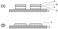
- FIG. 1 (1) to (2) and FIGS. 2 (3) to 2 (4) are schematic cross-sectional views showing a state of manufacture. That is, it shows the assembly process flow for constructing the cushioning adhesive layer.
- FIG. 1 (1) is a first joining step in which the first joining material 5 is joined onto the first substrate 1, pre-dried, and then electronic components are mounted and joined.
- the die 4 is bonded to the spacer 3 by using the third bonding material 6.
- An insulating substrate can be used as the first substrate 1, and for example, it can be a DBC substrate or a TPC substrate in which a circuit pattern is arranged on one side.
- the spacer 3 is a conductive metal plate and can be Cu.
- the die 4 is a semiconductor chip, and can be made of SiC or GaN in addition to Si.
- the first bonding material 5 and the third bonding material 6 are similar sintered materials. Joining using a sintered material is usually performed by applying a sintered material, pre-drying, and then pressurizing and heating the object to be joined. Further, by pre-drying, the shape of the bonding material can be kept flat.
- FIG. 1 (2) is a second joining step of joining the second joining material 7 on the second substrate 2.
- the second substrate 2 an insulating substrate similar to that of the first substrate 1 can be used.
- the second bonding material 7 is a sintered material similar to the first bonding material 5 and the third bonding material 6, and can be manufactured by a method of printing a paste-like material and applying it to a substrate. Keep free of pre-drying process.
- FIG. 1 (3) shows a third portion in which the electronic components (spacer 3 and die 4) bonded to the first substrate 1 and the second bonding material 7 bonded to the second substrate 2 are bonded facing each other. It is a joining process.
- Each bonding material becomes a sintered bonding layer, but the first bonding material 5 and the third bonding material 6 are pre-dried, so that they can be hardened and maintain a flat shape. Also. Since the second bonding material 7 is not pre-dried, it remains in a softened state.
- the substrate formed in the third joining step described above is placed in the reflow lower jig 8 and covered with the reflow upper jig 9. Tension is applied between the first substrate 1 and the second substrate 2 from the inside using a special metal jig 10. Then, it is a fourth joining step of heating and joining.
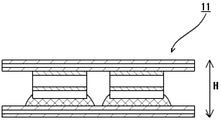
- FIG. 3 shows a state taken out from the reflow jig after the above-mentioned fourth joining step.
- a double-sided cooling power module is completed by resin molding between the substrates with a mold resin.
- the mold resin and the external lead-out terminal are as seen in the prior art, and are not shown here.
- the second bonding material 7 when the second bonding material 7 is bonded in a softened state, it is crushed into a fillet shape and becomes a buffer bonding layer (buffer adhesive layer).
- the second bonding material 7 absorbs the dimensions as a buffer even if the thickness variation of the spacer 3 and the die 4 is large. , It is possible to maintain the thickness H of the target module (FIG. 3).
- the height of the stacked can be corrected. The same applies even if the stacking order of the spacers and dies is arbitrary.
- a location guide block In the case of a conventional reflow jig, it is called a location guide block and has a structure that is sandwiched between upper and lower jigs. Therefore, although the maximum height of the power module can be controlled, it is difficult to control the minimum height.
- the special metal jig 10 combines the reflow lower jig 8 and the reflow upper jig 9, and presses the substrate against the inner walls of the reflow lower jig 8 and the reflow upper jig 9 from the inside of the substrate.
- a special metal jig 10 is inserted inside each substrate, tensioned and used, and a buffer bonding layer (2nd bonding material 7 which is the last flowable adhesive layer under the die 4 is used.
- a buffer bonding layer 2nd bonding material 7 which is the last flowable adhesive layer under the die 4 is used.
- the double-sided cooling power module can be controlled to a certain height, it will not be affected by the variation in the thickness of the members to be laminated, and when it is incorporated into a unit or equipment, there will be no gap between it and the heat sink (water jacket). High thermal performance can be maintained because it can be contacted.
- the number of electronic components may be one or a plurality, and the combination of the spacer 3 and the die 4 and the stacking order may be freely changed.
- the second bonding material may be arranged between "board and die”, “die and spacer”, or “spacer and substrate”. The effect is the same.
- spacer As the spacer, Cu / Mo or the like can be applied in addition to Cu.
- a tape or paste type can be used as the bonding material before pre-drying.
Landscapes
- Cooling Or The Like Of Semiconductors Or Solid State Devices (AREA)
Abstract
【課題】両面冷却パワーモジュールにおいて、積み重ねられた材料の厚さのばらつきがあるため、1つずつ積み重ねることは、全体の積層厚さを一定に抑えることは困難である。 【解決手段】材料厚さ公差がモジュール全体の厚さ公差に直接影響する場合、両面冷却モジュールの積層高さを制御するために、向かいあう絶縁基板にダイなどを積層して取り付けた後、基板に最後に取り付ける接合材(接着剤)を、特殊金属治具を使用し、予備乾燥をしないリフロープロセスで、緩衝接合層(バッファー接着層)とすることである。
Description
本発明は、パワー半導体パッケージの両面冷却(デュアルサイドクーリング:DUAL SIDE COOLING:DSC)パワーモジュールに関する。特に、内部に部材が積層されたパッケージの厚さを制御する製造方法とそのモジュールに関する。
現在のパワー半導体市場において、高電圧および高電流を使用するハイエンドパワーモジュールは、より効率的な放熱を必要とされている。特に、パワー半導体パッケージの両面冷却パワーモジュールは、高い電力密度と高速による半導体チップの高い動作温度に応じて、より高い熱性能を必要とされる。
例えば、特許文献1には、下端ターミナル、パワー半導体チップ、水平スペーサ、上端ターミナル、垂直スペーサで構成され、内部にこれら部材が積層された両面冷却パワーモジュールが開示されている。
従来方法で部材を積層する場合は、ダイマウント工程の前に印刷された接合材(接着剤)を使用して乾式処理(ドライプロセス)を実行するが、印刷された接合材の表面の平坦性が不均一であるため、次工程でチップクラックや絶縁基板にクラックが発生する懸念がある。
また、積み重ねられた材料の厚さのばらつきがあるため、1つずつ積み重ねることは、接合材乾燥工程なしの従来方法では、全体の積層厚さを一定に抑えることは困難である。
材料厚さ公差がモジュール全体の厚さ公差に直接影響する場合、両面冷却モジュールの積層高さを制御するために、向かいあう絶縁基板にダイなどを積層して取り付けた後、基板に最後に取り付ける接合材(接着剤)を、特殊金属治具を使用し、予備乾燥をしないリフロープロセスで、緩衝接合層(バッファー接着層)とすることである。
乾式工程を含まない最後の接合材層は、特殊金属治具を使用して、原材料と積層材料の厚さのばらつきをすべて緩衝接合層として補正することができる。これにより、パワー半導体の両面冷却(デュアルサイドクーリングモジュール)のスタック高さ(H)のばらつきを従来よりも小さくすることがでる。
さらに、パワー半導体は、ウォータージャケット冷却システムに適合する熱性能を最適化できる。すなわち、安い部材(寸法公差を緩和部材)が使用でき、パワー半導体のパッケージ厚さを均一にできる。
以下、本発明を実施するための形態について、図を参照して詳細に説明する。ただし、本発明は以下の記載に何ら限定されるものではない。
本発明の実施例1に係る両面冷却パワーモジュールの製造方法を図1で説明する。図1(1)~(2)、図2(3)~(4)は、製造の状態を示した断面略図である。すなわち緩衝接着剤層を構築する組み立てプロセスフローを示している。
図1(1)は、第一の基板1上に第一の接合材5を接合し予備乾燥させた後、電子部品を搭載し接合する第一の接合工程である。ここで電子部品は、スペーサ3上に、ダイ4を第三の接合材6を用いて接合したのである。
第一の基板1は、絶縁基板が使用でき、例えば、一方に回路パターンが配置されたDBC基板やTPC基板とすることができる。スペーサ3は、導電性金属板であり、Cuとすることができる。ダイ4は、半導体チップであり、Siの他、SiC、GaNのとすることができる。
第一の接合材5と第三の接合材6とは同様な焼結材である。焼結材を用いた接合は、通常焼結材を塗布し、予備乾燥後に接合対象物を加圧加熱し接合するものである。また、予備乾燥することによって、接合材の形状が平坦に保てる。
図1(2)は、第二の基板2上に第二の接合材7を接合する第二の接合工程である。ここでは、第二の基板2は、第一の基板1と同様な絶縁基板が使用できる。第二の接合材7は、第一の接合材5、第三の接合材6とは同様な焼結材であり、ペースト状材料を印刷して基板に塗布する方法で製造することができ、予備乾燥プロセスを用いない状態を保つ。
図1(3)は、第一の基板1に接合された電子部品(スペーサ3とダイ4)と第二の基板2に接合された第二の接合材7を向かい合わせて接合する第三の接合工程である。
各接合材は焼結結合層となるが、第一の接合材5、第三の接合材6は、予備乾燥するので、硬化し平坦な形状を保つことができる。また。第二の接合材7は、予備乾燥しないので、軟化した状態を保っている。
図1(4)は、前述の第三の接合工程で形成された基板をリフロー下治具8に入れ、リフロー上治具9を覆いかぶせる。第一の基板1と第二の基板2との間に内側から特殊金属治具10を用いて、テンションを加える。そして、加熱し接合する第四の接合工程である。
図3は、前述の第四の接合工程後にリフロー治具から取り出した状態である。通常、基板間をモールド樹脂により樹脂成形をして両面冷却パワーモジュールが完成する。ここでは、モールド樹脂、外部導出端子は先行技術に見られるようなものであり、図示を省略している。
ここで、第二の接合材7は、軟化した状態で接合されると、押しつぶされフィレット形状となり、緩衝接合層(バッファー接着層)となる。
すなわち、第二の接合材7は、バッファーとしての予備乾燥されていない軟化状態の接着層を使用することにより、スペーサ3やダイ4の厚さばらつきが大きい場合でも、その寸法をバッファーとして吸収し、目標モジュールの厚さH(図3)を維持することが可能である。
スペーサやダイが複数の場合であっても、積み重ねた高さを補正することができる。また、スペーサやダイの積層順番が任意の場合であっても同様である。
完成した両面冷却パワーモジュールの樹脂分解と断面分析により、他のパワー半導体モジュールの積層構造とは、フィレット形状が異なることが確認できる。
従来のリフロー治具の場合、ロケーションガイドブロックと言われ、上下治具で挟み込む構造である。そのため、パワーモジュールの最大高さは制御できるが、最小高さを制御するのは困難である。
そのため、本発明は、特殊金属治具10は、リフロー下治具8とリフロー上治具9を組み合わせ、基板内側から基板をリフロー下治具8、リフロー上治具9の内壁に押し付けるように、特殊金属治具10をそれぞれの基板内側に挿入し、テンションをかけて使用し、ダイ4の下の流動可能な最後の接着層である第二の接合材7を使用して、緩衝接合層(バッファー接着層)とすることにより、積層厚さHを補正することにより、一定の高さに制御できる。
両面冷却パワーモジュールを一定の高さに制御できれば、の積層する部材の厚さのばらつきに左右されず、ユニットや機器に組み込む場合、ヒートシンク(ウォータージャケット)との間に隙間ができず、十分に接触できるため高い熱性能を維持できる。
電子部品は、ひとつでも複数でもよく、スペーサ3とダイ4の組み合わせや積層順番は自由に変えてもよい。
また、第二の接合材は、「基板とダイ」の他、「ダイとスペーサ」、または「スペーサと基板」の間に配置してもよい。その効果は同じである。
また、スペーサは、Cuの他、Cu / Moなどが適用することができる。
また、厚さのばらつきが補正されていれば、予備乾燥前の接合材はテープやペーストタイプを使用することができる。
1、第一の基板
2、第二の基板
3、スペーサ
4、ダイ(チップ)
5、第一の接合材
6、第三の接合材
7、第二の接合材(緩衝接合層)
8、リフロー下治具
9、リフロー上治具
10、特殊金属治具
11、パワーモジュール
2、第二の基板
3、スペーサ
4、ダイ(チップ)
5、第一の接合材
6、第三の接合材
7、第二の接合材(緩衝接合層)
8、リフロー下治具
9、リフロー上治具
10、特殊金属治具
11、パワーモジュール
Claims (5)
- 第一の基板上に第一の接合材を接合し予備乾燥させた後、電子部品を搭載し接合する第一の接合工程と、第二の基板上に第二の接合材を接合する第二の接合工程と、前記第一の基板に接合された前記電子部品と前記第二の基板に接合された前記第二の接合材を向かい合わせて接合する第三の接合工程と、前記第一の基板と前記第二の基板との間にテンションを加え、加熱し接合する第四の接合工程とからなる両面冷却パワーモジュールの製造方法。
- 前記第一ないし前記二の接合材は、焼結材料であり、銀、銅、酸化銀、および酸化銅からなり少なくとも一種を含み、ペースト状態、または、テープ状態からなることを特徴とする請求項1に記載の両面冷却パワーモジュールの製造方法。
- 前記電子部品は、半導体チップ、スペーサまたは、それらの組み合わせSiの他、SiC、GaNからなることを特徴とする請求項1ないし請求項2に記載の両面冷却パワーモジュールの製造方法。
- 前記第一の基板と前記第二の基板は、DBC(Direct Bonded Copper)基板からなることを特徴とする請求項1ないし請求項3に記載の両面冷却パワーモジュールの製造方法。
- 請求項1ないし請求項4に記載の製造方法で製造され、第一の接合材は平坦な形状からなる焼結結合層であり、第二の接合材はフィレット形状からなる緩衝接合層(バッファー接着層)であることを特徴とする両面冷却パワーモジュール。
Priority Applications (3)
| Application Number | Priority Date | Filing Date | Title |
|---|---|---|---|
| CN202080103447.5A CN115868021A (zh) | 2020-09-01 | 2020-09-01 | 双面冷却功率模块的制造方法以及双面冷却功率模块 |
| JP2022546754A JP7644129B2 (ja) | 2020-09-01 | 2020-09-01 | 両面冷却パワーモジュールの製造方法 |
| PCT/JP2020/033128 WO2022049641A1 (ja) | 2020-09-01 | 2020-09-01 | 両面冷却パワーモジュールの製造方法、および両面冷却パワーモジュール |
Applications Claiming Priority (1)
| Application Number | Priority Date | Filing Date | Title |
|---|---|---|---|
| PCT/JP2020/033128 WO2022049641A1 (ja) | 2020-09-01 | 2020-09-01 | 両面冷却パワーモジュールの製造方法、および両面冷却パワーモジュール |
Publications (1)
| Publication Number | Publication Date |
|---|---|
| WO2022049641A1 true WO2022049641A1 (ja) | 2022-03-10 |
Family
ID=80490759
Family Applications (1)
| Application Number | Title | Priority Date | Filing Date |
|---|---|---|---|
| PCT/JP2020/033128 Ceased WO2022049641A1 (ja) | 2020-09-01 | 2020-09-01 | 両面冷却パワーモジュールの製造方法、および両面冷却パワーモジュール |
Country Status (3)
| Country | Link |
|---|---|
| JP (1) | JP7644129B2 (ja) |
| CN (1) | CN115868021A (ja) |
| WO (1) | WO2022049641A1 (ja) |
Cited By (1)
| Publication number | Priority date | Publication date | Assignee | Title |
|---|---|---|---|---|
| WO2025033127A1 (ja) | 2023-08-04 | 2025-02-13 | パナソニックIpマネジメント株式会社 | 接合シート、半導体装置、半導体装置の製造方法及び半導体装置の製造装置 |
Citations (3)
| Publication number | Priority date | Publication date | Assignee | Title |
|---|---|---|---|---|
| JPH10303228A (ja) * | 1997-04-23 | 1998-11-13 | Hitachi Ltd | 圧接型半導体装置 |
| WO2017043545A1 (ja) * | 2015-09-07 | 2017-03-16 | 日立化成株式会社 | 接合用銅ペースト、接合体の製造方法及び半導体装置の製造方法 |
| JP2017191857A (ja) * | 2016-04-13 | 2017-10-19 | 株式会社デンソー | 電子装置及びその製造方法 |
Family Cites Families (6)
| Publication number | Priority date | Publication date | Assignee | Title |
|---|---|---|---|---|
| JP2012174747A (ja) * | 2011-02-18 | 2012-09-10 | Calsonic Kansei Corp | パワー半導体モジュールの構造およびその製造方法 |
| KR102208961B1 (ko) * | 2013-10-29 | 2021-01-28 | 삼성전자주식회사 | 반도체소자 패키지 및 그 제조방법 |
| KR102730548B1 (ko) * | 2018-12-06 | 2024-11-13 | 현대자동차주식회사 | 양면 냉각형 파워모듈 및 그 제조 방법 |
| KR20200071596A (ko) * | 2018-12-11 | 2020-06-19 | 현대자동차주식회사 | 양면 냉각 파워모듈의 높이 제어방법 |
| CN111524877B (zh) * | 2019-02-03 | 2022-03-18 | 株洲中车时代半导体有限公司 | 一种双面散热功率模块 |
| CN111584443A (zh) * | 2020-05-26 | 2020-08-25 | 忱芯科技(上海)有限公司 | 双面散热功率模块及其双面平行度的控制方法 |
-
2020
- 2020-09-01 JP JP2022546754A patent/JP7644129B2/ja active Active
- 2020-09-01 WO PCT/JP2020/033128 patent/WO2022049641A1/ja not_active Ceased
- 2020-09-01 CN CN202080103447.5A patent/CN115868021A/zh active Pending
Patent Citations (3)
| Publication number | Priority date | Publication date | Assignee | Title |
|---|---|---|---|---|
| JPH10303228A (ja) * | 1997-04-23 | 1998-11-13 | Hitachi Ltd | 圧接型半導体装置 |
| WO2017043545A1 (ja) * | 2015-09-07 | 2017-03-16 | 日立化成株式会社 | 接合用銅ペースト、接合体の製造方法及び半導体装置の製造方法 |
| JP2017191857A (ja) * | 2016-04-13 | 2017-10-19 | 株式会社デンソー | 電子装置及びその製造方法 |
Cited By (1)
| Publication number | Priority date | Publication date | Assignee | Title |
|---|---|---|---|---|
| WO2025033127A1 (ja) | 2023-08-04 | 2025-02-13 | パナソニックIpマネジメント株式会社 | 接合シート、半導体装置、半導体装置の製造方法及び半導体装置の製造装置 |
Also Published As
| Publication number | Publication date |
|---|---|
| JPWO2022049641A1 (ja) | 2022-03-10 |
| JP7644129B2 (ja) | 2025-03-11 |
| CN115868021A (zh) | 2023-03-28 |
Similar Documents
| Publication | Publication Date | Title |
|---|---|---|
| JP6171622B2 (ja) | パワーモジュール用基板、パワーモジュール及びパワーモジュール用基板を製造する方法 | |
| CN101952960B (zh) | 低温加压烧结的方法 | |
| CN102132403B (zh) | 模制超薄半导体管芯封装和使用该封装的系统及其制造方法 | |
| JP5484429B2 (ja) | 電力変換装置 | |
| KR20150049265A (ko) | 반도체소자 패키지 및 그 제조방법 | |
| WO2009110376A1 (ja) | リードフレーム基板、半導体モジュール、及びリードフレーム基板の製造方法 | |
| JP2018133527A (ja) | 半導体装置及び半導体装置の製造方法 | |
| JP2001177006A (ja) | 熱伝導基板とその製造方法 | |
| JP2014072304A (ja) | 半導体モジュールの製造方法、半導体モジュール | |
| JP6183166B2 (ja) | ヒートシンク付パワーモジュール用基板及びその製造方法 | |
| JP7644129B2 (ja) | 両面冷却パワーモジュールの製造方法 | |
| JP2024025271A (ja) | 半導体モジュールの製造方法 | |
| US20220051964A1 (en) | Baseplate for a semiconductor module and method for producing a baseplate | |
| WO2022162871A1 (ja) | 両面冷却パワーモジュール | |
| CN114242664B (zh) | 一种低应力高导热的igbt功率模块封装结构 | |
| KR20240114018A (ko) | 적층형 파워 모듈 및 그 제조 방법 | |
| KR20240043915A (ko) | 파워모듈 및 이의 제조방법 | |
| JP5542853B2 (ja) | 半導体装置および半導体装置の製造方法 | |
| KR102260662B1 (ko) | 체결형 스페이서를 이용한 양면냉각모듈패키지 및 그의 제조방법 | |
| JP2004281676A (ja) | 放熱板及び放熱板の製造方法 | |
| TWI576930B (zh) | Circuit package of circuit component module and its product | |
| KR20190112992A (ko) | 전력 변환기용 반도체 모듈 및 이의 제조 방법 | |
| JP3985558B2 (ja) | 熱伝導性基板の製造方法 | |
| JP4779668B2 (ja) | 積層基板の製造方法 | |
| JP2002270731A (ja) | 配線基板及びその製造方法、並びに半導体装置 |
Legal Events
| Date | Code | Title | Description |
|---|---|---|---|
| 121 | Ep: the epo has been informed by wipo that ep was designated in this application |
Ref document number: 20952381 Country of ref document: EP Kind code of ref document: A1 |
|
| ENP | Entry into the national phase |
Ref document number: 2022546754 Country of ref document: JP Kind code of ref document: A |
|
| NENP | Non-entry into the national phase |
Ref country code: DE |
|
| 122 | Ep: pct application non-entry in european phase |
Ref document number: 20952381 Country of ref document: EP Kind code of ref document: A1 |