WO2022034797A1 - 多端子積層コンデンサ - Google Patents
多端子積層コンデンサ Download PDFInfo
- Publication number
- WO2022034797A1 WO2022034797A1 PCT/JP2021/027872 JP2021027872W WO2022034797A1 WO 2022034797 A1 WO2022034797 A1 WO 2022034797A1 JP 2021027872 W JP2021027872 W JP 2021027872W WO 2022034797 A1 WO2022034797 A1 WO 2022034797A1
- Authority
- WO
- WIPO (PCT)
- Prior art keywords
- internal electrode
- terminal
- slit
- vias
- external terminals
- Prior art date
- Legal status (The legal status is an assumption and is not a legal conclusion. Google has not performed a legal analysis and makes no representation as to the accuracy of the status listed.)
- Ceased
Links
Images


Classifications
-
- H—ELECTRICITY
- H01—ELECTRIC ELEMENTS
- H01G—CAPACITORS; CAPACITORS, RECTIFIERS, DETECTORS, SWITCHING DEVICES, LIGHT-SENSITIVE OR TEMPERATURE-SENSITIVE DEVICES OF THE ELECTROLYTIC TYPE
- H01G4/00—Fixed capacitors; Processes of their manufacture
- H01G4/002—Details
- H01G4/228—Terminals
- H01G4/232—Terminals electrically connecting two or more layers of a stacked or rolled capacitor
-
- H—ELECTRICITY
- H01—ELECTRIC ELEMENTS
- H01G—CAPACITORS; CAPACITORS, RECTIFIERS, DETECTORS, SWITCHING DEVICES, LIGHT-SENSITIVE OR TEMPERATURE-SENSITIVE DEVICES OF THE ELECTROLYTIC TYPE
- H01G4/00—Fixed capacitors; Processes of their manufacture
- H01G4/002—Details
- H01G4/005—Electrodes
- H01G4/012—Form of non-self-supporting electrodes
-
- H—ELECTRICITY
- H01—ELECTRIC ELEMENTS
- H01G—CAPACITORS; CAPACITORS, RECTIFIERS, DETECTORS, SWITCHING DEVICES, LIGHT-SENSITIVE OR TEMPERATURE-SENSITIVE DEVICES OF THE ELECTROLYTIC TYPE
- H01G4/00—Fixed capacitors; Processes of their manufacture
- H01G4/30—Stacked capacitors
-
- H—ELECTRICITY
- H01—ELECTRIC ELEMENTS
- H01G—CAPACITORS; CAPACITORS, RECTIFIERS, DETECTORS, SWITCHING DEVICES, LIGHT-SENSITIVE OR TEMPERATURE-SENSITIVE DEVICES OF THE ELECTROLYTIC TYPE
- H01G4/00—Fixed capacitors; Processes of their manufacture
- H01G4/38—Multiple capacitors, i.e. structural combinations of fixed capacitors
- H01G4/385—Single unit multiple capacitors, e.g. dual capacitor in one coil
-
- H—ELECTRICITY
- H01—ELECTRIC ELEMENTS
- H01G—CAPACITORS; CAPACITORS, RECTIFIERS, DETECTORS, SWITCHING DEVICES, LIGHT-SENSITIVE OR TEMPERATURE-SENSITIVE DEVICES OF THE ELECTROLYTIC TYPE
- H01G4/00—Fixed capacitors; Processes of their manufacture
- H01G4/002—Details
- H01G4/018—Dielectrics
- H01G4/06—Solid dielectrics
- H01G4/08—Inorganic dielectrics
- H01G4/12—Ceramic dielectrics
Definitions
- the present invention relates to a multi-terminal multilayer capacitor.
- Patent Document 1 a capacitor main body, a first internal electrode and a second internal electrode alternately arranged so as to face each other with each layer of the laminated dielectric layer sandwiched between them, and a first surface formed on one or more of the upper and lower surfaces of the main body. It is composed of a first external terminal, a second external terminal, and a first conductive via hole and a second conductive via hole formed in the stacking direction of the main body and connected to the first external terminal and the second external terminal, respectively. Stacked capacitor arrays are disclosed. In particular, in this laminated capacitor array, in order to reduce ESL, the magnetic fields induced by the currents flowing through the internal electrodes connected to the first conductive via holes and the second conductive via holes are mutually canceled. (Alternate arrangement).
- Patent Document 2 in order to reduce ESL, the internal electrode and the external terminal electrode are connected via the via hole conductor, and the via hole conductor penetrates through the internal electrode electrically insulated from the via hole conductor.
- a laminated capacitor in which an island-shaped punching portion is formed in a portion to be formed is disclosed.
- a plurality of island-shaped punching portions are connected to each other, and a punching connecting portion is formed so as to connect the outer side portions of the internal electrodes and the island-shaped punching portions. That is, a punching connection portion is formed so as to divide (divide) the internal electrodes into a plurality of regions isolated from each other.
- the internal electrodes are divided (divided) into a plurality of regions by the unplugged connecting portion, so that the characteristics such as capacitance and ESR (equivalent series resistance) may deteriorate. , And the mechanical strength of the element may decrease. In particular, these problems may become noticeable when the vias are arranged at a narrow pitch.
- the present invention has been made to solve the above-mentioned problems, and it is possible to suppress a decrease in capacitance (effective value) while maintaining a low ESL in a high frequency region, and to secure mechanical strength of an element. It is an object of the present invention to provide a possible multi-terminal multilayer capacitor.
- the multi-terminal laminated capacitor according to the present invention is arranged inside a first internal electrode and a second internal electrode alternately laminated via a dielectric layer, and inside the first internal electrode and the second internal electrode in a plan view.
- a plurality of first external terminals connected to each of the plurality of first vias and a plurality of second external terminals connected to each of the plurality of second vias, and the first via is a first via a first slit.
- the plurality of regions are arranged so as to be electrically connected, and the second via is divided into a plurality of regions by a second slit.
- the plurality of regions are arranged so as to be electrically connected to each other.
- the first via when the first internal electrode is divided into a plurality of regions by the first slit, the first via is arranged so as to electrically connect the plurality of regions.
- the second internal electrode is divided into a plurality of regions by the two slits, the second via is arranged so as to electrically connect the plurality of regions. Therefore, it is avoided that the first and second internal electrodes are divided (divided) into a plurality of regions isolated from each other. Then, when a voltage is applied to the first and second external terminals, a common voltage is applied to the first and second internal electrodes, respectively, through the conduction connection with the first and second vias.
- the capacity can be increased as compared with the case where the internal electrode is electrically divided (divided). Further, since the multi-terminal laminated capacitor is composed of two conductors as a whole, it is possible to suppress the occurrence of an unnecessary resonance mode at high frequencies.
- a first slit is formed so as to extend between the first insulating portion formed around the second via penetrating the first internal electrode and insulating the second via and the first internal electrode, and the first via.
- a second slit is formed so as to extend between the second insulating portion formed around the first via penetrating the second internal electrode and insulating the first via and the second internal electrode, and the second via.
- the voltage drop seen in the axial direction of the first and second vias becomes small, and the decrease in capacitance in the high frequency region is alleviated (that is, the frequency characteristic of the capacitance is flattened).
- the effect of reducing ESR and ESL can be obtained.
- first vias are arranged inside the first internal electrode and the second internal electrode in a plan view
- second vias are arranged inside the first internal electrode and the second internal electrode in a plan view.
- the first and second vias are not arranged on the outer edges of the first and second internal electrodes. Therefore, the outer edge (outer circumference) of the first and second internal electrodes is not divided by the first and second slits. Therefore, the mechanical strength of the element can be ensured.
- FIG. 3 is a cross-sectional view taken along the line II-II of FIG.
- FIG. 3 is a cross-sectional view taken along the line III-III of FIG.
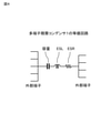
- It is a figure which shows the equivalent circuit of the multi-terminal laminated capacitor which concerns on 1st Embodiment.
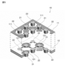
- It is an exploded perspective view which shows the internal structure of the multi-terminal laminated capacitor which concerns on 1st Embodiment.
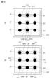
- It is a top view which shows the structure of (a) 1st internal electrode, (b) the 2nd internal electrode which comprises the multi-terminal laminated capacitor which concerns on 1st Embodiment.
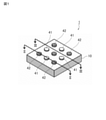
- FIG. 1 is a perspective view showing the configuration of the multi-terminal laminated capacitor 1.
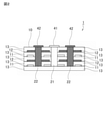
- FIG. 2 is a cross-sectional view taken along the line II-II of FIG.
- FIG. 3 is a cross-sectional view taken along the line III-III of FIG.
- FIG. 4 is a diagram showing an equivalent circuit of the multi-terminal multilayer capacitor 1.
- minute L (inductance) and R (resistance) are parasitic on the first and second external terminals 41 and 42, but in the equivalent circuit shown in FIG. 4, these parasitic L and R are ESL. And ESR, and the direct display was omitted.
- FIG. 5 is an exploded perspective view showing the internal structure of the multi-terminal laminated capacitor 1.
- FIG. 6 is a plan view showing the configurations of (a) the first internal electrode 11 and (b) the second internal electrode 12 constituting the multi-terminal laminated capacitor 1.
- the multi-terminal laminated capacitor 1 includes, for example, a laminated body 10 formed in a rectangular parallelepiped shape, nine external terminals 41 and 42 formed on the top surface (upper surface) of the laminated body 10, and more specifically, four first terminals. It includes one external terminal 41 and five second external terminals 42.
- the laminated body 10 is configured by alternately laminating the first internal electrode 11 and the second internal electrode 12 so as to face each other via a plurality of dielectric layers (insulator layers) 13 formed in a rectangular shape.
- the dielectric layer 13 is formed of, for example, a dielectric ceramic containing Badio 3, CaTIO 3 , SrTiO 3 , CaZrO 3 , and the like as main components.
- auxiliary components such as Mn compound, Fe compound, Cr compound, Co compound, and Ni compound may be added to these main components.
- the first internal electrode 11 and the second internal electrode 12 are formed, for example, in the form of a rectangular thin film.
- Each of the first internal electrode 11 and the second internal electrode 12 is formed of, for example, Ni, Cu, Ag, Pd, Ag—Pd alloy, Au, or the like.
- the laminate 10 is arranged inside the first internal electrode 11 and the second internal electrode 12 (that is, without touching the outer edge) in a plan view, and is electrically connected (conducted) to the first internal electrode 11.
- a plurality of (four in this embodiment) first vias 21 are formed so as to be insulated from the second internal electrode 12 and penetrate the laminated body 10 in the laminated direction (thickness direction).
- the laminate 10 is arranged inside the first internal electrode 11 and the second internal electrode 12 (that is, without touching the outer edge) in a plan view, and is electrically connected to the second internal electrode 12 (that is, without touching the outer edge).
- a plurality of (five in this embodiment) second vias 22 are formed so as to be conductive and insulated from the first internal electrode 11 and penetrate the laminated body 10 in the laminating direction (thickness direction).
- a plurality of (4) first external terminals 41 are connected to the ends of each of the plurality (4) first vias 21.
- a plurality of (five) second external terminals 42 are connected to the ends of each of the plurality (five) second vias 22.
- the first external terminal 41 and the second external terminal 42 are formed of, for example, a conductive material containing silver as a main component.
- the first external terminal 41 (first via 21) and the second external terminal 42 (second via 22) are arranged alternately and in a matrix shape in a plan view.
- the configuration was set.
- the first internal electrode 11 has an annular first insulating portion (opening) formed around the second via 22 penetrating the first internal electrode 11 and insulating the second via 22 and the first internal electrode 11. 111 is formed. Further, a linear first slit (gap) 31 is formed so as to extend between the first insulating portion 111 and the first via 21.
- the second internal electrode 12 has an annular second insulating portion (which is formed around the first via 21 penetrating the second internal electrode 12 and insulates the first via 21 and the second internal electrode 12.
- the opening) 121 is formed.
- a linear second slit (gap) 32 is formed so as to extend between the second insulating portion 121 and the second via 22.
- the first slit 31 and the second slit 32 are formed in a grid pattern (a grid pattern) of 3 rows and 3 columns.
- the shapes of the first and second slits 31 and 32 are not limited to 3 rows and 3 columns, and can be arbitrarily set according to requirements and the like (the same applies hereinafter). Further, in the present embodiment, the first slit 31 and the second slit 32 are formed so as to overlap (match) in a plan view.
- the first internal electrode 11 when the first internal electrode 11 is divided into a plurality of regions (five regions in the present embodiment) by the first slit 31, the first via 21 electrically connects (conducts) the plurality of regions. ). Therefore, the first internal electrode 11 is a single internal electrode having a common potential.
- the second internal electrode 12 when the second internal electrode 12 is divided into a plurality of regions (five regions in the present embodiment) by the second slit 32, the second via 22 electrically connects (conducts) the plurality of regions. ). Therefore, the second internal electrode 12 becomes a single internal electrode having a common potential.
- the first internal electrode 11 when the first internal electrode 11 is divided into a plurality (five) regions by the first slit 31, the plurality of regions are electrically divided.
- the first via 21 is arranged so as to be connected (conducting) and the second internal electrode 12 is divided into a plurality (five) regions by the second slit 32, the plurality of regions are electrically connected.
- the second via 22 is arranged so as to be (conducting). Therefore, it is avoided that the first and second internal electrodes 11 and 12 are divided (divided) into a plurality of regions isolated from each other.
- the first and second internal electrodes 11 and 12 are common to the first and second internal electrodes 11 and 12, respectively, through conduction connection with the first and second vias 21 and 22. Voltage is applied. Therefore, the capacity can be increased as compared with the case where the internal electrode is electrically divided (divided). Further, since the multi-terminal laminated capacitor 1 is composed of two conductors as a whole, it is possible to suppress the generation of unnecessary resonance modes at high frequencies.
- the first slit 31 is formed so as to extend between the first insulating portion 111 that insulates the second via 22 and the first internal electrode 11 and the first via 21.
- a second slit 32 is formed so as to extend between the second insulating portion 121 that insulates the 1 via 21 and the second internal electrode 12 and the second via 22. Therefore, when the first and second vias 21 and 22 are viewed in a cross section including the center thereof and the first and second slits 31 and 32, the conductors along the axial direction of the first and second vias 21 and 22. The surface path is shortened. As a result, the impedance along the axial direction of the first and second vias 21 and 22 is reduced.
- the voltage drop seen in the axial direction of the first and second vias 21 and 22 becomes small, and the decrease in capacitance in the high frequency region is alleviated (that is, the frequency characteristic of the capacitance is flattened).
- the effect of reducing ESR and ESL can be obtained.
- the plurality of first vias 21 and the plurality of second vias 22 are inside the first internal electrode 11 and the second internal electrode 12 (that is, without touching the outer edge) in a plan view. ) Be placed. That is, the first and second vias 21 and 22 are not arranged on the outer edges of the first and second internal electrodes 11 and 12. Therefore, the outer edges (outer circumferences) of the first and second internal electrodes 11 and 12 are not divided by the first and second slits 31 and 32. Therefore, the mechanical strength of the element can be ensured, and the flatness of the element can be ensured.
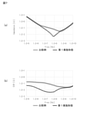
- FIG. 7 shows (a) impedance characteristics and (b) ESR characteristics of the multi-terminal multilayer capacitor 1 and the comparative example according to the present embodiment.
- FIG. 7A shows the impedance characteristics (simulation results) of the multi-terminal laminated capacitor 1 and the comparative example
- FIG. 7B shows the ESR characteristics (simulation results) of the multi-terminal laminated capacitor 1 and the comparative example.
- the horizontal axis of the graph of FIG. 7A is frequency (Hz), and the vertical axis is impedance ( ⁇ ). Further, the horizontal axis of the graph of (b) is frequency (Hz), and the vertical axis is ESR ( ⁇ ).
- FIG. 7A it was confirmed that the impedance (particularly, the impedance near 100 MHz) is lower than that of the comparative example according to the multi-terminal multilayer capacitor 1. Further, as shown in FIG. 7B, it was confirmed that the ESR was lowered according to the multi-terminal laminated capacitor 1 as compared with the comparative example.
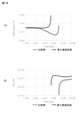
- FIG. 8 shows (a) capacitance characteristics and (b) ESL characteristics of the multi-terminal laminated capacitor 1 and the comparative example.
- FIG. 8A shows the capacitance characteristics (simulation results) of the multi-terminal laminated capacitor 1 and the comparative example
- FIG. 8B shows the ESL characteristics (simulation results) of the multi-terminal laminated capacitor 1 and the comparative example.
- the horizontal axis of the graph of FIG. 8A is frequency (Hz), and the vertical axis is capacitance (F).
- the horizontal axis of the graph of (b) is frequency (Hz)
- the vertical axis is ESL (H).
- the first slit 31 and the second slit 32 are formed in a grid pattern, but as shown in FIG. 9, the first slit 31B and the second slit 32 are formed.
- the second slit 32B may be formed into three linear shapes extending parallel to the contours of the first internal electrode 11B and the second internal electrode 12B.
- FIG. 9 is a plan view showing the configurations of (a) the first internal electrode 11B and (b) the second internal electrode 12B constituting the multi-terminal laminated capacitor 1B according to the second embodiment.
- the first slit 31B and the second slit 32B are formed so as to overlap (match) in a plan view.
- the first and second internal electrodes 11B and 12B do not have an electrically divided (divided) region. Since other configurations are the same as or similar to those of the multi-terminal multilayer capacitor 1 according to the first embodiment described above, detailed description thereof will be omitted here.
- FIG. 10 shows (a) impedance characteristics and (b) ESR characteristics of the multi-terminal multilayer capacitor 1B and the comparative example according to the present embodiment.
- FIG. 10A shows the impedance characteristics (simulation results) of the multi-terminal laminated capacitor 1B and the comparative example
- FIG. 10B shows the ESR characteristics (simulation results) of the multi-terminal laminated capacitor 1B and the comparative example.
- the horizontal axis of the graph of FIG. 10A is frequency (Hz), and the vertical axis is impedance ( ⁇ ).
- the horizontal axis of the graph of (b) is frequency (Hz), and the vertical axis is ESR ( ⁇ ).
- the impedance (particularly, the impedance near 100 MHz) is lower than that of the comparative example according to the multi-terminal multilayer capacitor 1B. Further, as shown in FIG. 10B, it was confirmed that the ESR was lowered as compared with the comparative example according to the multi-terminal laminated capacitor 1B. That is, it was confirmed that the multi-terminal laminated capacitor 1B according to the second embodiment can also exert the same effect as the multi-terminal laminated capacitor 1 according to the first embodiment described above.
- FIG. 11 shows (a) capacitance characteristics and (b) ESL characteristics of the multi-terminal laminated capacitor 1B and the comparative example.
- FIG. 11A shows the capacitance characteristics (simulation results) of the multi-terminal laminated capacitor 1B and the comparative example
- FIG. 11B shows the ESL characteristics (simulation results) of the multi-terminal laminated capacitor 1B and the comparative example.
- the horizontal axis of the graph of FIG. 11A is frequency (Hz), and the vertical axis is capacitance (F).
- the horizontal axis of the graph of (b) is frequency (Hz)
- the vertical axis is ESL (H).
- FIG. 11A in the comparative example, a decrease in capacitance was observed in the high frequency region (particularly in the region of 10 MHz or more), but according to the multi-terminal multilayer capacitor 1B, the high frequency region (particularly 10 MHz) was observed. It was confirmed that the capacity did not decrease even in the above area). Further, as shown in FIG. 11B, it was confirmed that the ESL can be maintained low according to the multi-terminal laminated capacitor 1B. That is, it was confirmed that the multi-terminal laminated capacitor 1B according to the second embodiment can also exert the same effect as the multi-terminal laminated capacitor 1 according to the first embodiment described above.
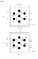
- FIG. 12 is a plan view showing the configurations of (a) the first internal electrode 11B and (b) the second internal electrode 12C constituting the multi-terminal laminated capacitor 1C according to the third embodiment.
- the first slit 31B and the second slit 32C are configured to be orthogonal to each other. Therefore, in the present embodiment, the first slit 31B and the second slit 32C do not overlap (that is, do not match) in a plan view. Further, in this case, the first and second internal electrodes 11B and 12C do not have an electrically divided (divided) region. Since other configurations are the same as or similar to those of the multi-terminal multilayer capacitor 1B according to the second embodiment described above, detailed description thereof will be omitted here.
- the magnetic fields entering and exiting the first slit 31B and the second slit 32C are linear. Although it is not distributed (that is, it deviates from the optimum conditions), it is possible to obtain almost the same effect as the multi-terminal laminated capacitor 1B according to the second embodiment described above.
- the widths of the first slit 31 and the second slit 32 are constant, but as shown in FIG. 13, the first via 21 of the first slit 31D and the first via 21
- the contact portion (connection portion) of the above may be formed in a tapered shape that narrows toward the contact portion.
- the contact portion (connecting portion) of the second slit 32D with the second via 22 may be formed in a tapered shape that narrows toward the contact portion.
- FIG. 13 is a plan view showing the configurations of (a) the first internal electrode 11D and (b) the second internal electrode 12D constituting the multi-terminal laminated capacitor 1D according to the fourth embodiment. Since other configurations are the same as or similar to those of the multi-terminal multilayer capacitor 1 according to the first embodiment described above, detailed description thereof will be omitted here.
- the first and second slits 31D and 32D in a tapered shape, conduction connection between the first and second internal electrodes 11D and 12D and the first and second vias 21 and 22 can be established. It can be achieved reliably, and the influence of misalignment (variation) can be reduced. Further, when the element is fired in the manufacturing process, the element shrinks similarly, but by forming the first and second slits 31D and 32D in a tapered shape, the shapes of the first and second slits 31D and 32D are formed even after firing. Can be well secured (maintained).
- a land pattern may be provided at the connection portion between the first and second vias 21 and 22 and the first and second slits 31 and 32 with respect to the multi-terminal laminated capacitor 1 according to the first embodiment described above.
- connection portion of the first internal electrode 11E with the first via 21 is formed in an annular shape. That is, an annular first land pattern 112E is formed around the first via 21 penetrating the first internal electrode 11E.
- connection portion of the second internal electrode 12E with the second via 22 is formed in an annular shape. That is, an annular second land pattern 122E is formed around the second via 22 penetrating the second internal electrode 12E.
- FIG. 14 is a plan view showing the configurations of (a) the first internal electrode 11E and (b) the second internal electrode 12E constituting the multi-terminal laminated capacitor 1E according to the fifth embodiment.
- the first slit 31E is formed so as to connect the first insulating portion 111 and the first land pattern 112E (first via 21).
- the second slit 32E is formed so as to connect the second insulating portion 121 and the second land pattern 122E (second via 22).
- the diameters of the first and second land patterns 112E and 122E are larger than the widths of the first and second slits 31E and 32E, and larger than the diameters of the first and second vias 21 and 22. Since other configurations are the same as or similar to those of the multi-terminal multilayer capacitor 1 according to the first embodiment described above, detailed description thereof will be omitted here.
- the conduction connection between the first and second internal electrodes 11E and 12E and the first and second vias 21 and 22 is surely achieved. It is possible to reduce the influence of misalignment and the like (variation).
- first external terminal 41 first via 21
- second external terminal 42 second via 22
- first external terminal 41 first via 21
- second external terminal 42 second via 22
- first external terminal 41 first via 21
- second external terminal 42 second via 22
- FIG. 15 is a plan view showing the configurations of (a) the first internal electrode 11F and (b) the second internal electrode 12F constituting the multi-terminal laminated capacitor 1F according to the sixth embodiment. Further, FIG. 16 is an exploded perspective view showing the internal structure of the multi-terminal laminated capacitor 1F.
- the first and second external terminals 41 and 42 are aligned with the same polarity.
- the land pattern of the mounting board for example, mounting on a linear line such as a microstrip line or a coplanar line can be performed. It will be easy (possible).
- the ground signal ground (GSG) is arranged, and a through-type capacitor is connected to form a single chip. This facilitates handling at the time of mounting.
- FIG. 17 shows (a) impedance characteristics and (b) ESR characteristics of the multi-terminal multilayer capacitor 1F and the comparative example according to the present embodiment.
- FIG. 17A shows the impedance characteristics (simulation results) of the multi-terminal laminated capacitor 1F and the comparative example
- FIG. 17B shows the ESR characteristics (simulation results) of the multi-terminal laminated capacitor 1F and the comparative example.
- the horizontal axis of the graph of FIG. 17A is frequency (Hz), and the vertical axis is impedance ( ⁇ ). Further, the horizontal axis of the graph of (b) is frequency (Hz), and the vertical axis is ESR ( ⁇ ).
- the impedance (particularly, the impedance of 100 MHz or less) is lower than that of the comparative example according to the multi-terminal laminated capacitor 1F.
- FIG. 17B it was confirmed that the ESR was lowered as compared with the comparative example according to the multi-terminal laminated capacitor 1F. That is, it was confirmed that the multi-terminal laminated capacitor 1F according to the sixth embodiment can also exert the same effect as the multi-terminal laminated capacitor 1B according to the second embodiment described above.
- FIG. 18 shows (a) capacitance characteristics and (b) ESL characteristics of the multi-terminal laminated capacitor 1F and the comparative example.
- FIG. 18A shows the capacitance characteristics (simulation results) of the multi-terminal laminated capacitor 1F and the comparative example
- FIG. 18B shows the ESL characteristics (simulation results) of the multi-terminal laminated capacitor 1F and the comparative example.
- the horizontal axis of the graph of FIG. 18A is frequency (Hz), and the vertical axis is capacitance (F).
- the horizontal axis of the graph of (b) is frequency (Hz)
- the vertical axis is ESL (H).
- FIG. 18A in the comparative example, a decrease in capacitance was observed in the high frequency region (particularly in the region of 10 MHz or more), but according to the multi-terminal multilayer capacitor 1F, the high frequency region (particularly 10 MHz) was observed. It was confirmed that the capacity did not decrease even in the above area). Further, as shown in FIG. 18B, it was confirmed that the ESL can be maintained relatively low according to the multi-terminal laminated capacitor 1F, although it is slightly higher than that of the comparative example. That is, it was confirmed that the multi-terminal laminated capacitor 1F according to the sixth embodiment can also exert almost the same effect as the multi-terminal laminated capacitor 1B according to the second embodiment described above.
- a plurality of (two in this embodiment) first external terminals 41 (first via 21) are viewed in a plan view. Are linearly aligned (that is, aligned with the same polarity), and a plurality of (three in this embodiment) second external terminals 42 (second vias 22) are linearly aligned (that is, aligned with the same polarity).
- FIG. 19 is a plan view showing the configurations of (a) the first internal electrode 11G and (b) the second internal electrode 12G constituting the multi-terminal laminated capacitor 1G according to the seventh embodiment. Since other configurations are the same as or similar to those of the multi-terminal multilayer capacitor 1 (according to the first embodiment) described above, detailed description thereof will be omitted here.
- the first and second external terminals 41 and 42 are aligned with the same polarity.
- the land pattern of the mounting board for example, mounting on a linear line such as a microstrip line or a coplanar line can be performed. It will be easy (possible).
- the ground signal ground (GSG) is arranged, and a through-type capacitor is connected to form a single chip. This facilitates handling at the time of mounting.
- the multi-terminal multilayer capacitor 1G according to the present embodiment can also exert the same effect as the multi-terminal multilayer capacitor 1F according to the sixth embodiment described above.
- FIG. 20 is a plan view showing the configurations of (a) the first internal electrode 11G and (b) the second internal electrode 12H constituting the multi-terminal laminated capacitor 1H according to the eighth embodiment.
- the first slit 31G and the second slit 32H do not overlap (that is, do not match) in a plan view. Since other configurations are the same as or similar to those of the multi-terminal multilayer capacitor 1G according to the seventh embodiment described above, detailed description thereof will be omitted here.
- the first and second external terminals 41 and 42 are aligned with the same polarity.
- the land pattern of the mounting board for example, mounting on a linear line such as a microstrip line or a coplanar line can be performed. It will be easy (possible).
- the ground signal ground (GSG) is arranged, and a through-type capacitor is connected to form a single chip. This facilitates handling at the time of mounting.
- the surface paths of the first and second vias 21 and 22 and the first and second internal electrodes 11G and 12H are long, and the current path through the first and second slits 31G and 32H is the shortest. It disappears.
- the impedance and ESR of the current path increase, and the Joule loss of the multi-terminal laminated capacitor 1H as a whole also increases.
- the second external terminal 42 (second via 22) is arranged alternately and in a staggered pattern (that is, shifted by half a pitch), but as shown in FIG. 21, it is linear.
- a plurality of (three) aligned first external terminals 41 (first via 21) and a plurality of (two) linearly aligned second external terminals 42 (second via 22) are alternately arranged.
- the configuration may be such that they are arranged in a staggered pattern (that is, offset by half a pitch) (8 terminals).
- the first slit 31J is formed in an oblique direction (y-shaped) with respect to the contour of the first internal electrode 11J
- the second slit 32J is formed with respect to the contour of the second internal electrode 12J. It was formed in an oblique direction (y-shaped).
- 21 is a plan view showing the configurations of (a) the first internal electrode 11J and (b) the second internal electrode 12J constituting the multi-terminal laminated capacitor 1J according to the ninth embodiment. Since other configurations are the same as or similar to those of the multi-terminal multilayer capacitor 1G according to the seventh embodiment described above, detailed description thereof will be omitted here.
- the first and second external terminals 41 and 42 have the same polarity.
- the land pattern of the mounting board By aligning) and designing the land pattern of the mounting board according to the arrangement of the first and second external terminals 41 and 42, for example, mounting on a linear line such as a microstrip line or a coplanar line. Is easy (possible).
- the ground signal ground (GSG) is arranged, and a through-type capacitor is connected to form a single chip. This facilitates handling at the time of mounting.
- the multi-terminal multilayer capacitor 1J according to the present embodiment can also exert the same effect as the multi-terminal multilayer capacitor 1G according to the seventh embodiment described above.
- FIG. 22 is a plan view showing the configurations of (a) the first internal electrode 11K and (b) the second internal electrode 12K constituting the multi-terminal laminated capacitor 1K according to the tenth embodiment. Since other configurations are the same as or similar to those of the multi-terminal multilayer capacitor 1F according to the sixth embodiment described above, detailed description thereof will be omitted here.
- the areas of the first and second internal electrodes 11K and 12K are increased.
- the capacity of the multi-terminal laminated capacitor 1K increases as a whole.
- the widths of the first slit 31F and the second slit 32F are constant, but as shown in FIG. 23, the widths of the first slit 31L and the first via 21 are constant.
- the contact portion (connection portion) of the above may be formed in a tapered shape that narrows toward the contact portion.
- the contact portion (connecting portion) of the second slit 32L with the second via 22 may be formed in a tapered shape that narrows toward the contact portion.
- FIG. 23 is a plan view showing the configurations of (a) the first internal electrode 11L and (b) the second internal electrode 12L constituting the multi-terminal laminated capacitor 1L according to the eleventh embodiment. Since other configurations are the same as or similar to those of the multi-terminal multilayer capacitor 1F according to the sixth embodiment described above, detailed description thereof will be omitted here.
- the first and second slits 31L and 32L in a tapered shape, conduction connection between the first and second internal electrodes 11L and 12L and the first and second vias 21 and 22 can be established. It can be achieved reliably, and the influence of misalignment (variation) can be reduced. Further, when the element is fired in the manufacturing process, the element shrinks similarly, but by forming the first and second slits 31L and 32L in a tapered shape, the shapes of the first and second slits 31L and 32L are formed even after firing. Can be well secured (maintained).
- a land pattern may be provided at the connection portion between the first and second vias 21 and 22 and the first and second slits 31F and 32F.
- connection portion of the first internal electrode 11M with the first via 21 is formed in an annular shape. That is, an annular first land pattern 112M is formed around the first via 21 penetrating the first internal electrode 11M.
- connection portion of the second internal electrode 12M with the second via 22 is formed in an annular shape. That is, an annular second land pattern 122M is formed around the second via 22 penetrating the second internal electrode 12M.
- FIG. 24 is a plan view showing the configurations of (a) the first internal electrode 11M and (b) the second internal electrode 12M constituting the multi-terminal laminated capacitor 1M according to the twelfth embodiment.
- the first slit 31M is formed so as to connect the first insulating portion 111 and the first land pattern 112M (first via 21).
- the second slit 32M is formed so as to connect the second insulating portion 121 and the second land pattern 122M (second via 22). Since other configurations are the same as or similar to those of the multi-terminal multilayer capacitor 1F according to the sixth embodiment described above, detailed description thereof will be omitted here.
- the conduction connection between the first and second internal electrodes 11M and 12M and the first and second vias 21 and 22 is surely achieved. It is possible to reduce the influence of misalignment and the like (variation).
- the present invention is not limited to the above embodiments and can be modified in various ways.
- the number and arrangement (arrangement) of the first and second vias 21 and 22 and the first and second external terminals 41 and 42 described above, and the shape and arrangement of the first and second slits 31 and 32 and the like. Is an example and can be set arbitrarily according to the requirements and the like.
Landscapes
- Engineering & Computer Science (AREA)
- Power Engineering (AREA)
- Manufacturing & Machinery (AREA)
- Microelectronics & Electronic Packaging (AREA)
- Fixed Capacitors And Capacitor Manufacturing Machines (AREA)
- Ceramic Capacitors (AREA)
Priority Applications (3)
| Application Number | Priority Date | Filing Date | Title |
|---|---|---|---|
| CN202180057206.6A CN116075913B (zh) | 2020-08-12 | 2021-07-28 | 多端子层叠电容器 |
| JP2022542624A JP7537500B2 (ja) | 2020-08-12 | 2021-07-28 | 多端子積層コンデンサ |
| US18/101,132 US12300439B2 (en) | 2020-08-12 | 2023-01-25 | Multi-terminal multilayer capacitor |
Applications Claiming Priority (2)
| Application Number | Priority Date | Filing Date | Title |
|---|---|---|---|
| JP2020-136462 | 2020-08-12 | ||
| JP2020136462 | 2020-08-12 |
Related Child Applications (1)
| Application Number | Title | Priority Date | Filing Date |
|---|---|---|---|
| US18/101,132 Continuation US12300439B2 (en) | 2020-08-12 | 2023-01-25 | Multi-terminal multilayer capacitor |
Publications (1)
| Publication Number | Publication Date |
|---|---|
| WO2022034797A1 true WO2022034797A1 (ja) | 2022-02-17 |
Family
ID=80247204
Family Applications (1)
| Application Number | Title | Priority Date | Filing Date |
|---|---|---|---|
| PCT/JP2021/027872 Ceased WO2022034797A1 (ja) | 2020-08-12 | 2021-07-28 | 多端子積層コンデンサ |
Country Status (4)
| Country | Link |
|---|---|
| US (1) | US12300439B2 (https=) |
| JP (1) | JP7537500B2 (https=) |
| CN (1) | CN116075913B (https=) |
| WO (1) | WO2022034797A1 (https=) |
Citations (4)
| Publication number | Priority date | Publication date | Assignee | Title |
|---|---|---|---|---|
| JP2001148325A (ja) * | 1999-11-19 | 2001-05-29 | Murata Mfg Co Ltd | 積層コンデンサ、配線基板、デカップリング回路および高周波回路 |
| JP2002160467A (ja) * | 2000-11-27 | 2002-06-04 | Murata Mfg Co Ltd | スクリーン印刷版、スクリーン印刷方法、および積層コンデンサ |
| JP2003059755A (ja) * | 2001-08-09 | 2003-02-28 | Murata Mfg Co Ltd | 積層型電子部品およびその製造方法 |
| JP2006135333A (ja) * | 2004-11-04 | 2006-05-25 | Samsung Electro Mech Co Ltd | 積層型キャパシターアレイ及びその配線接続構造 |
Family Cites Families (7)
| Publication number | Priority date | Publication date | Assignee | Title |
|---|---|---|---|---|
| JP3337018B2 (ja) * | 1999-11-19 | 2002-10-21 | 株式会社村田製作所 | 積層コンデンサ、配線基板、デカップリング回路および高周波回路 |
| JP2002260959A (ja) | 2001-03-01 | 2002-09-13 | Nec Corp | 積層コンデンサとその製造方法およびこのコンデンサを用いた半導体装置、電子回路基板 |
| KR100674830B1 (ko) * | 2004-11-04 | 2007-01-25 | 삼성전기주식회사 | 적층형 캐패시터 어레이 |
| KR100649579B1 (ko) * | 2004-12-07 | 2006-11-28 | 삼성전기주식회사 | 적층형 캐패시터 및 적층형 캐패시터 어레이 |
| WO2015025642A1 (ja) * | 2013-08-21 | 2015-02-26 | 株式会社村田製作所 | 電気化学素子用セラミック基体及びその製造方法並びに燃料電池及び燃料電池スタック |
| KR102691325B1 (ko) * | 2016-11-01 | 2024-08-05 | 삼성전기주식회사 | 적층 전자부품 |
| JP7388088B2 (ja) * | 2018-10-30 | 2023-11-29 | Tdk株式会社 | 積層セラミック電子部品とその製造方法 |
-
2021
- 2021-07-28 JP JP2022542624A patent/JP7537500B2/ja active Active
- 2021-07-28 CN CN202180057206.6A patent/CN116075913B/zh active Active
- 2021-07-28 WO PCT/JP2021/027872 patent/WO2022034797A1/ja not_active Ceased
-
2023
- 2023-01-25 US US18/101,132 patent/US12300439B2/en active Active
Patent Citations (4)
| Publication number | Priority date | Publication date | Assignee | Title |
|---|---|---|---|---|
| JP2001148325A (ja) * | 1999-11-19 | 2001-05-29 | Murata Mfg Co Ltd | 積層コンデンサ、配線基板、デカップリング回路および高周波回路 |
| JP2002160467A (ja) * | 2000-11-27 | 2002-06-04 | Murata Mfg Co Ltd | スクリーン印刷版、スクリーン印刷方法、および積層コンデンサ |
| JP2003059755A (ja) * | 2001-08-09 | 2003-02-28 | Murata Mfg Co Ltd | 積層型電子部品およびその製造方法 |
| JP2006135333A (ja) * | 2004-11-04 | 2006-05-25 | Samsung Electro Mech Co Ltd | 積層型キャパシターアレイ及びその配線接続構造 |
Also Published As
| Publication number | Publication date |
|---|---|
| CN116075913B (zh) | 2025-09-09 |
| JP7537500B2 (ja) | 2024-08-21 |
| US20230162919A1 (en) | 2023-05-25 |
| CN116075913A (zh) | 2023-05-05 |
| JPWO2022034797A1 (https=) | 2022-02-17 |
| US12300439B2 (en) | 2025-05-13 |
Similar Documents
| Publication | Publication Date | Title |
|---|---|---|
| US7466535B2 (en) | Multilayer capacitor | |
| US7508647B2 (en) | Multilayer capacitor | |
| US7312975B2 (en) | Laminated capacitor and manufacturing method thereof | |
| US20070279836A1 (en) | Monolithic capacitor and mounting structure thereof | |
| KR101083983B1 (ko) | 적층 콘덴서의 제조 방법 | |
| JP2014036214A (ja) | 積層コンデンサ | |
| JPH1126243A (ja) | 複合電子部品 | |
| US20080225463A1 (en) | Layered capacitor and mounting structure | |
| US7164184B2 (en) | Multilayer capacitor | |
| JP6273672B2 (ja) | 積層貫通コンデンサ | |
| JP2874695B1 (ja) | 積層型電子部品アレイ | |
| JP2007042677A (ja) | 積層コンデンサ | |
| JP4618362B2 (ja) | 積層コンデンサの製造方法 | |
| JP5093044B2 (ja) | 積層コンデンサ | |
| JPH07161568A (ja) | 積層コンデンサアレイ | |
| JP3230586B2 (ja) | 非可逆回路素子用中心導体及び非可逆回路素子 | |
| JP7537500B2 (ja) | 多端子積層コンデンサ | |
| JP2996233B1 (ja) | 積層型コイル部品 | |
| JP2007019101A (ja) | 積層型電子部品 | |
| JP2010177696A (ja) | 積層コンデンサ | |
| JP4539440B2 (ja) | 積層コンデンサの実装構造 | |
| JP4412386B2 (ja) | 貫通型積層コンデンサ | |
| JP2001110638A (ja) | 積層電子部品 | |
| JP3104958U (ja) | 低キャパシタンス積層可変抵抗器 | |
| JP2010093193A (ja) | 積層コンデンサ |
Legal Events
| Date | Code | Title | Description |
|---|---|---|---|
| 121 | Ep: the epo has been informed by wipo that ep was designated in this application |
Ref document number: 21855876 Country of ref document: EP Kind code of ref document: A1 |
|
| ENP | Entry into the national phase |
Ref document number: 2022542624 Country of ref document: JP Kind code of ref document: A |
|
| NENP | Non-entry into the national phase |
Ref country code: DE |
|
| 122 | Ep: pct application non-entry in european phase |
Ref document number: 21855876 Country of ref document: EP Kind code of ref document: A1 |
|
| WWG | Wipo information: grant in national office |
Ref document number: 202180057206.6 Country of ref document: CN |