WO2022030320A1 - 劣化検出用プリント基板 - Google Patents
劣化検出用プリント基板 Download PDFInfo
- Publication number
- WO2022030320A1 WO2022030320A1 PCT/JP2021/027827 JP2021027827W WO2022030320A1 WO 2022030320 A1 WO2022030320 A1 WO 2022030320A1 JP 2021027827 W JP2021027827 W JP 2021027827W WO 2022030320 A1 WO2022030320 A1 WO 2022030320A1
- Authority
- WO
- WIPO (PCT)
- Prior art keywords
- circuit board
- printed circuit
- wiring
- deterioration detection
- back surface
- Prior art date
- Legal status (The legal status is an assumption and is not a legal conclusion. Google has not performed a legal analysis and makes no representation as to the accuracy of the status listed.)
- Ceased
Links
Images



Classifications
-
- H—ELECTRICITY
- H05—ELECTRIC TECHNIQUES NOT OTHERWISE PROVIDED FOR
- H05K—PRINTED CIRCUITS; CASINGS OR CONSTRUCTIONAL DETAILS OF ELECTRIC APPARATUS; MANUFACTURE OF ASSEMBLAGES OF ELECTRICAL COMPONENTS
- H05K1/00—Printed circuits
- H05K1/02—Details
- H05K1/0266—Marks, test patterns or identification means
- H05K1/0268—Marks, test patterns or identification means for electrical inspection or testing
-
- H—ELECTRICITY
- H05—ELECTRIC TECHNIQUES NOT OTHERWISE PROVIDED FOR
- H05K—PRINTED CIRCUITS; CASINGS OR CONSTRUCTIONAL DETAILS OF ELECTRIC APPARATUS; MANUFACTURE OF ASSEMBLAGES OF ELECTRICAL COMPONENTS
- H05K1/00—Printed circuits
- H05K1/02—Details
- H05K1/0296—Conductive pattern lay-out details not covered by sub groups H05K1/02 - H05K1/0295
-
- H—ELECTRICITY
- H05—ELECTRIC TECHNIQUES NOT OTHERWISE PROVIDED FOR
- H05K—PRINTED CIRCUITS; CASINGS OR CONSTRUCTIONAL DETAILS OF ELECTRIC APPARATUS; MANUFACTURE OF ASSEMBLAGES OF ELECTRICAL COMPONENTS
- H05K2203/00—Indexing scheme relating to apparatus or processes for manufacturing printed circuits covered by H05K3/00
- H05K2203/16—Inspection; Monitoring; Aligning
- H05K2203/163—Monitoring a manufacturing process
Definitions
- the present invention relates to a deterioration detection printed circuit board attached to a main printed circuit board that is a target of deterioration detection.
- Machine tools are used in an environment where cutting fluid containing foreign substances such as chloride and sulfide is scattered.
- cutting fluid adheres to the main printed circuit board of a machine tool, the copper foil part of the wiring pattern corrodes and breaks.
- a printed circuit board for deterioration detection is attached to the main printed circuit board in order to predict the disconnection of the wiring pattern.
- the deterioration detection printed circuit board has a deterioration detection wiring pattern that is more easily broken than the wiring pattern of the main printed circuit board.
- the deterioration detection printed circuit board has an insulator substrate and a wiring pattern formed on both sides of the insulator substrate.
- the wiring pattern is deteriorated by the adhesion of mist-like cutting fluid scattered in the space.
- the wiring pattern is deteriorated by the adhesion of the cutting fluid flowing on the surface of the main printed circuit board or the cutting fluid flowing on the surface of the insulator substrate.
- the manufacturing cost of the printed circuit board for deterioration detection increases.
- Japanese Unexamined Patent Publication No. 2018-41837 discloses a deterioration detection printed circuit board having a wiring pattern on the back surface of the insulator substrate. No wiring pattern is formed on the surface of the insulator substrate. Therefore, according to Japanese Patent Application Laid-Open No. 2018-41837, it is possible to suppress the manufacturing cost of the printed circuit board for deterioration detection.
- a plurality of electrode pads connected to the wiring pattern of the main printed circuit board are provided on the back surface of the insulator board.
- the plurality of electrode pads are provided on the edge of the back surface in order to secure the bonding strength of the printed circuit board for deterioration detection with respect to the main printed circuit board. Further, flux scattered during soldering adheres around each electrode pad.
- the flux adhering to multiple electrode pads and their surroundings prevents the cutting fluid from entering the gap between the main printed circuit board and the detection printed circuit board.
- the cutting fluid is less likely to adhere to the wiring pattern formed on the back surface of the insulator substrate, and disconnection is less likely to occur.
- an object of the present invention is to provide a printed circuit board for deterioration detection capable of promoting disconnection of a wiring pattern without increasing the manufacturing cost.
- An aspect of the present invention is a deterioration detection printed circuit board having an insulator substrate and a deterioration detection wiring pattern formed on the outer surface of the insulator substrate, which is attached to a main printed circuit board to be targeted for deterioration detection.
- the wiring pattern is formed on the back surface of the outer surface of the insulator substrate, which is located on the main printed circuit board side, and the insulator substrate is located on the side opposite to the back surface from the back surface. It has a penetrating portion that penetrates to the surface.
- FIG. 1 is a schematic diagram of a main printed circuit board.
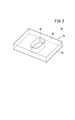
- FIG. 2 is a perspective view of the deterioration detection printed circuit board of the first embodiment.
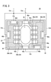
- FIG. 3 is a bottom view of the deterioration detection printed circuit board of the first embodiment.
- FIG. 4 is a perspective view of the deterioration detection printed circuit board of the second embodiment.
- FIG. 5 is a bottom view of the deterioration detection printed circuit board of the second embodiment.
- FIG. 1 is a schematic view of the main printed circuit board 10.
- the main printed circuit board 10 is used for a machine tool.
- a wiring pattern (not shown) of an electronic circuit is formed on at least one surface of the main printed circuit board 10, and a wiring pattern 12 of a deterioration detection circuit is formed.
- the main printed circuit board 10 is provided with a power supply terminal 14 and a ground terminal 16.
- the power supply terminal 14 is connected to a power supply.
- the ground terminal 16 is connected to the ground.
- the wiring pattern 12 includes a first wiring 12a, a second wiring 12b, a third wiring 12c, a fourth wiring 12d, and a fifth wiring 12e.
- the first end portion, which is one end of the first wiring 12a, is connected to the power supply terminal 14.
- the second end, which is the other end of the first wiring 12a is connected to the first electrode pad 40a of the deterioration detection printed circuit board 20, which will be described later.
- the first end portion, which is one end of the second wiring 12b is connected to the first electrode pad 40b of the deterioration detection printed circuit board 20.
- the second end, which is the other end of the second wiring 12b is connected to the first electrode pad 40c of the deterioration detection printed circuit board 20.
- the first end portion, which is one end of the third wiring 12c, is connected to the first electrode pad 40d of the deterioration detection printed circuit board 20.
- the second end, which is the other end of the third wiring 12c, is connected to the ground terminal 16.
- a resistor R is connected in series to the third wiring 12c.
- a voltage sensor V for detecting the resistance voltage is connected to both ends of the resistance R.
- the first end portion, which is one end of the fourth wiring 12d is connected to the second electrode pad 46a of the deterioration detection printed circuit board 20.
- the second end, which is the other end of the fourth wiring 12d is connected to the ground terminal 16.
- the first end portion, which is one end of the fifth wiring 12e is connected to the second electrode pad 46b of the deterioration detection printed circuit board 20.
- the second end, which is the other end of the fifth wiring 12e is connected to the ground terminal 16.
- the wiring pattern 12 shown in FIG. 1 is an example.
- the shape of the wiring pattern 12 is not limited to the shape shown in FIG.
- the wiring pattern 24 formed on the deterioration detection printed circuit board 20 has a wiring 42a and a wiring 42b.
- the wiring 42a is connected to the first electrode pad 40a and the first electrode pad 40b.
- the wiring 42b is connected to the first electrode pad 40c and the first electrode pad 40d.
- the first wiring 12a, the wiring 42a, the second wiring 12b, the wiring 42b, and the third wiring 12c are connected in series.
- the wiring 42a and the wiring 42b are thinner than the wiring (not shown) of the above-mentioned electronic circuit of the main printed circuit board 10. Therefore, the wiring 42a and the wiring 42b are likely to be disconnected.
- the voltage sensor V detects the resistance voltage.
- the voltage sensor V detects a zero voltage.
- the detection value of the voltage sensor V is an index indicating the degree of deterioration of the deterioration detection printed circuit board 20.
- the detected value of the voltage sensor V becomes an index indicating the degree of deterioration of the wiring pattern formed on the main printed circuit board 10.
- FIG. 2 is a perspective view of the deterioration detection printed circuit board 20 of the first embodiment.
- FIG. 3 is a bottom view of the deterioration detection printed circuit board 20 of the first embodiment.
- the deterioration detection printed circuit board 20 has an insulator substrate 22, a wiring pattern 24, and a solder resist 26.
- the solder resist 26 is indicated by dots.
- the outer shape of the wiring pattern 24 covered with the solder resist 26 is shown by a broken line.
- the insulator substrate 22 is a plate piece formed of an insulator member.
- the outer surface facing the main printed circuit board 10 is the back surface 32
- the outer surface facing the direction opposite to the direction in which the back surface 32 is directed is the front surface 30.
- the insulator substrate 22 has a through hole (penetration portion) 34 penetrating from a substantially central portion of the back surface 32 to a substantially central portion of the front surface 30.
- a general through hole cannot flow a liquid (cutting fluid).
- the size of the through hole 34 allows the liquid (cutting fluid) to flow from the front surface 30 to the back surface 32.
- the shape of the through hole 34 in a plan view is an oval. However, the shape of the through hole 34 is not limited to this.
- the wiring pattern 24 is made of a conductor such as copper and is printed on the back surface 32 of the insulator substrate 22.
- the wiring pattern 24 includes two sensor units 36a and 36b that are easily disconnected, and two disconnection promoting units 38a and 38b that promote disconnection of the sensor units 36a and 36b.
- the sensor unit 36a has the above-mentioned set of first electrode pads 40a and 40b and the wiring 42a.
- the first electrode pad 40a and the first electrode pad 40b are arranged on two facing edges of the plurality of edges of the back surface 32, respectively.
- the wiring 42a traverses the back surface 32 and passes around the through hole 34.
- the sensor unit 36b has the above-mentioned set of first electrode pads 40c and 40d and the wiring 42b.
- the first electrode pad 40c and the first electrode pad 40d are arranged on two facing edges of the plurality of edges of the back surface 32, respectively.
- the wiring 42b traverses the back surface 32 and passes around the through hole 34.
- the wiring 42a is arranged on one side (right side in FIG. 3) of the through hole 34 in the lateral direction.
- the wiring 42b is arranged on the other side (left side in FIG. 3) of the through hole 34 in the lateral direction.
- the wiring 42a and the wiring 42b are parallel to the longitudinal direction of the through hole 34.
- the wiring 42a and 42b are thin. Further, as will be described later, at least a part of the wiring 42a and at least a part of the wiring 42b are exposed to the atmosphere in the vicinity of the through hole 34. Therefore, the wirings 42a and 42b come into contact with the cutting fluid that flows from the front surface 30 through the through hole 34 and is guided to the back surface 32, and corrodes. As the corrosion progresses, each of the wiring 42a and the wiring 42b is disconnected.
- the disconnection promoting portion 38a is composed of one second electrode pad 46a and a ground portion 48a connected to the second electrode pad 46a.
- the second electrode pad 46a is arranged at the edge of the back surface 32.
- the ground portion 48a is adjacent to the wiring 42a at a predetermined distance.
- the disconnection promoting portion 38b is composed of one second electrode pad 46b and a ground portion 48b connected to the second electrode pad 46b.
- the second electrode pad 46b is arranged at the edge of the back surface 32.
- the ground portion 48b is adjacent to the wiring 42b at a predetermined interval.
- the shape of the wiring pattern 24 shown in FIG. 3 (shape and arrangement of the sensor portions 36a and 36b and the disconnection promoting portions 38a and 38b) is an example.
- the shape of the wiring pattern 24 is not limited to the shape shown in FIG.
- the solder resist 26 covers a part of each of the back surface 32, the wirings 42a and 42b, and the ground portions 48a and 48b.
- the solder resist 26 exposes a part of each of the back surface 32, the wirings 42a and 42b, and the ground portions 48a and 48b to the atmosphere. That is, a part of each of the wirings 42a and 42b and the ground portions 48a and 48b is covered with the solder resist 26. Further, a part of each of the wirings 42a and 42b and the ground portions 48a and 48b is exposed to the atmosphere.
- the wiring 42a in the outward direction of the portion where the wiring 42a is covered with the solder resist 26, there is a portion where the back surface 32 is covered with the solder resist 26.
- the disconnection promoting portion 38a In the outward direction of the portion where the back surface 32 is covered with the solder resist 26, there is a portion where the disconnection promoting portion 38a is covered with the solder resist 26.
- the wiring 42b, the disconnection promoting portion 38b, and the back surface 32 are also arranged in the same manner as the wiring 42a, the disconnection promoting portion 38a, and the back surface 32.
- the cutting fluid tends to collect at the boundary between the wiring pattern 24 and the solder resist 26.
- the boundary between the wiring 42a and the solder resist 26 is lined up around the through hole 34. Further, the boundary between the wiring 42b and the solder resist 26 is lined up around the through hole 34. According to such a structure, the cutting fluid that flows from the front surface 30 through the through hole 34 and is guided to the back surface 32 tends to collect at each boundary. Therefore, the wiring 42a is corroded and easily broken. In addition, the wiring 42b is corroded and easily broken.
- the cutting fluid adhering to the front surface 30 of the insulator substrate 22 flows through the through hole 34 and is guided to the back surface 32, and collects in the gap between the main printed circuit board 10 and the deterioration detection printed circuit board 20. .. Therefore, in the first embodiment, the disconnection of the wiring pattern 24 (wiring 42a, 42b) formed on the back surface 32 of the insulator substrate 22 can be promoted.
- the through hole 34 guides the cutting fluid adhering to the front surface 30 to the back surface 32. Therefore, it is not necessary to form the wiring pattern 24 on the surface 30 of the insulator substrate 22. Therefore, the deterioration detection printed circuit board 20 of the first embodiment can suppress an increase in manufacturing cost as compared with the deterioration detection printed circuit board in which the wiring pattern is formed on the front surface and the back surface.
- the wirings 42a and 42b are provided around the through hole 34. Further, the boundary between the wiring 42a and the solder resist 26 and the boundary between the wiring 42b and the solder resist 26 are arranged around the through hole 34.
- the first electrode pads 40a to 40d and the second electrode pads 46a and 46b are provided on the edge of the back surface 32 of the insulator substrate 22 and are not provided around the through hole 34. Therefore, the cutting fluid flowing to the back surface 32 comes into contact with the wirings 42a and 42b without being blocked by the first electrode pads 40a to 40d and the second electrode pads 46a and 46b. Further, the cutting fluid collects at the boundary between the wiring 42a and the solder resist 26. Further, the cutting fluid collects at the boundary between the wiring 42b and the solder resist 26. In the first embodiment, the disconnection of the wiring pattern 24 (wiring 42a, 42b) can be promoted even in such a point.
- FIG. 4 is a perspective view of the deterioration detection printed circuit board 20 of the second embodiment.
- FIG. 5 is a bottom view of the deterioration detection printed circuit board 20 of the second embodiment.
- the same components as those of the first embodiment are designated by the same reference numerals, and detailed description thereof will be omitted.
- the outer shape of the wiring pattern 24 covered with the solder resist 26 is shown by a broken line.
- the insulator substrate 22 of the second embodiment has a notch portion (penetration portion) 50 instead of the through hole 34 of the first embodiment.
- the cutout portion 50 is a portion in which a part of the insulator substrate 22 is cut out from the edge portion of the insulator substrate 22.
- a sensor unit 36a and a disconnection promoting unit 38a are provided on one side of the back surface 32 (on the right side in FIG. 5).
- a sensor unit 36b and a disconnection promoting unit 38b are provided on the other side of the back surface 32 (left side in FIG. 5).
- the first electrode pads 40a to 40d and the second electrode pads 46a and 46b are centrally provided on one edge of the back surface 32 of the insulator substrate 22.
- the second electrode pad 46a is provided between the first electrode pad 40a and the first electrode pad 40b.
- the second electrode pad 46b is provided between the first electrode pad 40c and the first electrode pad 40d.
- the wiring 42a is formed so as to pass through the two edges and the periphery of the notch 50.
- the ground portion 48a is located inside the wiring 42a.
- the wiring 42b is formed so as to pass through the two edges and the periphery of the notch 50.
- the ground portion 48b is located inside the wiring 42b.
- the shape of the wiring 42a and the shape of the wiring 42b are line-symmetrical with the center line C of the back surface 32 as the axis of symmetry.
- the shape of the ground portion 48a and the shape of the ground portion 48b are line-symmetrical with the center line C of the back surface 32 as the axis of symmetry.
- the second embodiment has the same effect as the first embodiment.
- the first electrode pads 40a to 40d and the second electrode pads 46a and 46b are concentrated on one edge of the back surface 32 of the insulator substrate 22. Therefore, the cutting fluid adhering to the main printed circuit board 10 easily penetrates into the gap between the main printed circuit board 10 and the deterioration detection printed circuit board 20.
- the shape of the wiring pattern 24 shown in FIG. 5 (shape and arrangement of the sensor portions 36a and 36b, shape and arrangement of the disconnection promoting portions 38a and 38b) is an example.
- the shape of the wiring pattern 24 is not limited to the shape shown in FIG.
- the solder resist 26 is provided.
- the entire wiring pattern 24 may not be covered with the solder resist 26 and may be exposed to the atmosphere.
- the probability of occurrence of corrosion and the probability of occurrence of disconnection of the wiring pattern 24 are lower than those of the first embodiment and the second embodiment.
- this modification also has a function of corroding the wiring pattern 24 (wiring 42a, 42b) and a function of disconnecting the wiring pattern 24 (wiring 42a, 42b). Has.
- the fineness of the wiring 42a and the fineness of the wiring 42b may be different.
- the resistance R connected to the wiring 42a and the resistance R connected to the wiring 42b may be different.
- the voltage sensor V connected to the wiring 42a and the voltage sensor V connected to the wiring 42b may be different.
- An aspect of the present invention includes an insulator substrate (22) and a wiring pattern (24) for detecting deterioration formed on the outer surface of the insulator substrate, and is a main printed circuit board (10) to be detected for deterioration. ),
- the wiring pattern is formed on the back surface (32) of the outer surface of the insulator substrate, which is located on the main printed circuit board side, and is the insulator.
- the substrate has a penetrating portion (34, 50) penetrating from the back surface to the surface surface (30) located on the side opposite to the back surface.
- the penetrating portion may be a through hole (34) penetrating the insulator substrate from the back surface to the front surface.
- the penetration portion may be a notch portion (50) in which a part of the insulator substrate is cut out from the edge portion of the insulator substrate.
- a solder resist (26) may be provided that covers the back surface and a part of the wiring pattern and exposes a part of the wiring pattern.
- a part of the wiring pattern exposed by the solder resist may be provided around the penetration portion.
- the printed circuit board for deterioration detection according to the present invention is not limited to the above-described embodiments and modifications, and of course, various configurations can be adopted without departing from the gist of the present invention.
Landscapes
- Engineering & Computer Science (AREA)
- Microelectronics & Electronic Packaging (AREA)
- Structure Of Printed Boards (AREA)
Abstract
絶縁体基板(22)と、絶縁体基板(22)の外面に形成される劣化検出用の配線パターン(24)と、を有し、劣化検出の対象となる主プリント基板(10)に取り付けられる劣化検出用プリント基板(20)であって、配線パターン(24)は、絶縁体基板(22)の外面のうち、主プリント基板(10)側に位置する裏面(32)に形成され、絶縁体基板(22)は、裏面(32)から裏面(32)とは反対側に位置する表面(30)にかけて貫通する貫通部(貫通孔(34)、切り欠き部(50))を有する。
Description
本発明は、劣化検出の対象となる主プリント基板に取り付けられる劣化検出用プリント基板に関する。
工作機械は、塩化物と硫化物等の異物を含む切削液が飛散する環境で使用される。工作機械の主プリント基板に切削液が付着すると、配線パターンの銅箔部分が腐食して断線する。配線パターンの断線を予測するために、主プリント基板には劣化検出用プリント基板が取り付けられる。劣化検出用プリント基板は、主プリント基板の配線パターンよりも断線しやすい劣化検出用の配線パターンを有する。
例えば、劣化検出用プリント基板は、絶縁体基板と、絶縁体基板の両面に形成される配線パターンと、を有する。配線パターンは、空間を飛散するミスト状の切削液が付着することによって劣化する。一方、配線パターンは、主プリント基板の表面を流れる切削液又は絶縁体基板の表面を流れる切削液が付着することによって劣化する。しかし、絶縁体基板の両面に配線パターンを形成する場合、劣化検出用プリント基板の製造コストが上昇する。
特開2018-41837号公報には、絶縁体基板の裏面に配線パターンを有する劣化検出用プリント基板が開示される。絶縁体基板の表面には、配線パターンが形成されない。このため、特開2018-41837号公報によれば、劣化検出用プリント基板の製造コストを抑制することができる。
絶縁体基板の裏面には、主プリント基板の配線パターンに接続される複数の電極パッドが設けられる。複数の電極パッドは、主プリント基板に対する劣化検出用プリント基板の接合強度を確保するために、裏面の縁部に設けられる。更に、各電極パッドの周囲には、はんだ付けの際に飛散するフラックスが付着する。
近時、複数の電極パッドとその周囲とに付着するフラックスが主プリント基板と検出用プリント基板との間の隙間に浸入しようとする切削液を阻む、ということが分かった。この場合、絶縁体基板の裏面に形成される配線パターンには切削液が付着しにくくなり、断線が発生しにくくなる。
そこで、本発明は、製造コストを上昇させることなく配線パターンの断線を促進させることができる劣化検出用プリント基板を提供することを目的とする。
本発明の態様は、絶縁体基板と、前記絶縁体基板の外面に形成される劣化検出用の配線パターンと、を有し、劣化検出の対象となる主プリント基板に取り付けられる劣化検出用プリント基板であって、前記配線パターンは、前記絶縁体基板の前記外面のうち、前記主プリント基板側に位置する裏面に形成され、前記絶縁体基板は、前記裏面から前記裏面とは反対側に位置する表面にかけて貫通する貫通部を有する。
本発明によれば、製造コストを上昇させることなく配線パターンの断線を促進させることができる。
本発明による劣化検出用プリント基板について、好適な実施形態を挙げ、添付の図面を参照しながら以下に詳細に説明する。
[1 主プリント基板10]
図1は、主プリント基板10の模式図である。主プリント基板10は、工作機械に使用される。主プリント基板10の少なくとも一方の面には、電子回路の配線パターン(不図示)が形成されるとともに、劣化検出回路の配線パターン12が形成される。また、主プリント基板10には、電源端子14と、グランド端子16と、が設けられる。電源端子14は、電源に接続される。グランド端子16は、グランドに接続される。
図1は、主プリント基板10の模式図である。主プリント基板10は、工作機械に使用される。主プリント基板10の少なくとも一方の面には、電子回路の配線パターン(不図示)が形成されるとともに、劣化検出回路の配線パターン12が形成される。また、主プリント基板10には、電源端子14と、グランド端子16と、が設けられる。電源端子14は、電源に接続される。グランド端子16は、グランドに接続される。
配線パターン12は、第1配線12aと、第2配線12bと、第3配線12cと、第4配線12dと、第5配線12eと、を有する。第1配線12aの一端である第1端部は電源端子14に接続される。第1配線12aの他端である第2端部は後述する劣化検出用プリント基板20の第1電極パッド40aに接続される。第2配線12bの一端である第1端部は劣化検出用プリント基板20の第1電極パッド40bに接続される。第2配線12bの他端である第2端部は劣化検出用プリント基板20の第1電極パッド40cに接続される。第3配線12cの一端である第1端部は劣化検出用プリント基板20の第1電極パッド40dに接続される。第3配線12cの他端である第2端部はグランド端子16に接続される。第3配線12cには、抵抗Rが直列に接続される。抵抗Rの両端には、抵抗電圧を検出する電圧センサVが接続される。第4配線12dの一端である第1端部は劣化検出用プリント基板20の第2電極パッド46aに接続される。第4配線12dの他端である第2端部はグランド端子16に接続される。第5配線12eの一端である第1端部は劣化検出用プリント基板20の第2電極パッド46bに接続される。第5配線12eの他端である第2端部はグランド端子16に接続される。
図1に示される配線パターン12は一例である。配線パターン12の形状は、図1に示される形状に限られない。
後述するが、劣化検出用プリント基板20に形成される配線パターン24は、配線42aと、配線42bと、を有する。配線42aは、第1電極パッド40aと第1電極パッド40bとに接続される。配線42bは、第1電極パッド40cと第1電極パッド40dとに接続される。第1配線12aと、配線42aと、第2配線12bと、配線42bと、第3配線12cとは、直列に接続される。配線42aと配線42bとは、主プリント基板10の前述した電子回路の配線(不図示)と比較して細い。このため、配線42aと配線42bと、は断線しやすい。配線42aと配線42b(及び第1配線12a~第3配線12c)とが断線していない状態で電源端子14に所定電圧が印加されると、電圧センサVは抵抗電圧を検出する。一方で、配線42a又は配線42bが断線している状態で電源端子14に所定電圧が印加されると、電圧センサVはゼロの電圧を検出する。このように、電圧センサVの検出値は、劣化検出用プリント基板20の劣化度合いを示す指標となる。結果として、電圧センサVの検出値は、主プリント基板10に形成される配線パターンの劣化度合いを示す指標となる。
[2 劣化検出用プリント基板20]
以下で劣化検出用プリント基板20の具体例として、第1実施形態と第2実施形態の説明をする。
以下で劣化検出用プリント基板20の具体例として、第1実施形態と第2実施形態の説明をする。
[2-1 第1実施形態]
図2は、第1実施形態の劣化検出用プリント基板20の斜視図である。図3は、第1実施形態の劣化検出用プリント基板20の底面図である。劣化検出用プリント基板20は、絶縁体基板22と、配線パターン24と、ソルダレジスト26と、を有する。なお、図3では、ソルダレジスト26はドットで示される。図3では、ソルダレジスト26で覆われる配線パターン24の外形箇所が破線で示される。
図2は、第1実施形態の劣化検出用プリント基板20の斜視図である。図3は、第1実施形態の劣化検出用プリント基板20の底面図である。劣化検出用プリント基板20は、絶縁体基板22と、配線パターン24と、ソルダレジスト26と、を有する。なお、図3では、ソルダレジスト26はドットで示される。図3では、ソルダレジスト26で覆われる配線パターン24の外形箇所が破線で示される。
絶縁体基板22は、絶縁体部材で形成される板片である。第1実施形態では、絶縁体基板22の外面のうち、主プリント基板10に向けられる外面を裏面32とし、裏面32が向けられる方向とは反対方向に向けられる外面を表面30とする。絶縁体基板22は、裏面32の略中心部分から表面30の略中心部分にかけて貫通する貫通孔(貫通部)34を有する。一般的なスルーホールは液体(切削液)を流し得ない。これに対して、貫通孔34の大きさは、液体(切削液)を表面30から裏面32に流し得る。第1実施形態において、貫通孔34の平面視の形状は、長円である。但し、貫通孔34の形状はこれに限定されない。
配線パターン24は、銅等の導体で形成されており、絶縁体基板22の裏面32にプリントされる。配線パターン24には、断線しやすい2つのセンサ部36a、36bと、センサ部36a、36bの断線を促進する2つの断線促進部38a、38bと、が含まれる。
センサ部36aは、前述した一組の第1電極パッド40a、40bと、配線42aと、を有する。第1電極パッド40aと第1電極パッド40bとは、裏面32の複数の縁部のうち、向かい合った2つの縁部にそれぞれ配置される。配線42aは、裏面32を縦断し、且つ、貫通孔34の周囲を通る。
センサ部36bは、前述した一組の第1電極パッド40c、40dと、配線42bと、を有する。第1電極パッド40cと第1電極パッド40dとは、裏面32の複数の縁部のうち、向かい合った2つの縁部にそれぞれ配置される。配線42bは、裏面32を縦断し、且つ、貫通孔34の周囲を通る。
配線42aは、貫通孔34の短手方向の一方側(図3の右側)に配置される。配線42bは、貫通孔34の短手方向の他方側(図3の左側)に配置される。配線42aと配線42bとは、貫通孔34の長手方向と平行する。
前述したように、配線42a、42bは細い。また、後述するが、配線42aの少なくとも一部と配線42bの少なくとも一部とは、貫通孔34の近傍で大気中に露出する。このため、配線42a、42bは、表面30から貫通孔34を流れて裏面32に案内される切削液と接触して腐食する。腐食が進行すると、配線42aと配線42bの各々は断線する。
断線促進部38aは、1つの第2電極パッド46aと、第2電極パッド46aに接続されるグランド部48aと、で構成される。第2電極パッド46aは、裏面32の縁部に配置される。グランド部48aは、配線42aと所定間隔離れて隣接する。
断線促進部38bは、1つの第2電極パッド46bと、第2電極パッド46bに接続されるグランド部48bと、で構成される。第2電極パッド46bは、裏面32の縁部に配置される。グランド部48bは、配線42bと所定間隔離れて隣接する。
図3に示される配線パターン24の形状(センサ部36a、36b及び断線促進部38a、38bの形状及び配置)は一例である。配線パターン24の形状は、図3に示される形状に限られない。
配線42aとグランド部48aとに跨って切削液が溜まり、且つ、配線42aとグランド部48aとの間に電位差が発生すると、配線42aからグランド部48aに銅イオンが移動する。すると、銅イオンの移動に伴い配線42aの腐食が進行して断線する。同様に、配線42bとグランド部48bとに跨って切削液が溜まり、且つ、配線42bとグランド部48bとの間に電位差が発生すると、配線42bからグランド部48bに銅イオンが移動する。すると、銅イオンの移動に伴い配線42bの腐食が進行して断線する。
ソルダレジスト26は、裏面32と、配線42a、42bと、グランド部48a、48bと、のそれぞれの一部を覆う。ソルダレジスト26は、裏面32と、配線42a、42bと、グランド部48a、48bと、のそれぞれの一部を大気中に露出させる。つまり、配線42a、42bと、グランド部48a、48bとのそれぞれの一部がソルダレジスト26で覆われる。また、配線42a、42bと、グランド部48a、48bとのそれぞれの一部が大気中に露出する。
貫通孔34の周囲には、配線42aが大気中に露出する部分と、配線42aがソルダレジスト26で覆われる部分とが交互に並ぶ。配線42aの外側方向には、断線促進部38aが大気中に露出する部分と、断線促進部38aがソルダレジスト26で覆われる部分とが交互に並ぶ。なお、配線42aが露出する部分の外側方向には、裏面32が大気中に露出する部分がある。裏面32が大気中に露出する部分の外側方向には、断線促進部38aが大気中に露出する部分がある。また、配線42aがソルダレジスト26で覆われる部分の外側方向には、裏面32がソルダレジスト26で覆われる部分がある。裏面32がソルダレジスト26で覆われる部分の外側方向には、断線促進部38aがソルダレジスト26で覆われる部分がある。なお、配線42bと断線促進部38bと裏面32も、配線42aと断線促進部38aと裏面32と同じように配置される。
切削液は、配線パターン24とソルダレジスト26との境界に溜まりやすい。配線42aとソルダレジスト26との境界が貫通孔34の周囲に並んでいる。また、配線42bとソルダレジスト26との境界が貫通孔34の周囲に並んでいる。こうした構造によると、表面30から貫通孔34を流れて裏面32に案内される切削液が各々の境界に溜まりやすい。このため、配線42aが腐食して断線しやすくなる。また、配線42bが腐食して断線しやすくなる。
第1実施形態において、絶縁体基板22の表面30に付着した切削液は、貫通孔34を流れて裏面32に案内され、主プリント基板10と劣化検出用プリント基板20との間の隙間に溜まる。従って、第1実施形態は、絶縁体基板22の裏面32に形成される配線パターン24(配線42a、42b)の断線を促進させることができる。第1実施形態によれば、貫通孔34が表面30に付着する切削液を裏面32に案内する。このため、配線パターン24を絶縁体基板22の表面30に形成する必要がない。このため、第1実施形態の劣化検出用プリント基板20は、配線パターンが表面と裏面とに形成される劣化検出用プリント基板と比較して、製造コストの上昇を抑制することができる。
また、第1実施形態において、配線42a、42bは貫通孔34の周囲に設けられる。更に、配線42aとソルダレジスト26との境界と、配線42bとソルダレジスト26との境界と、が貫通孔34の周囲に並べられる。その一方で、第1電極パッド40a~40dと第2電極パッド46a、46bとは絶縁体基板22の裏面32の縁部に設けられ、貫通孔34の周囲に設けられない。このため、裏面32に流れた切削液は、第1電極パッド40a~40dと第2電極パッド46a、46bとに阻まれることなく、配線42a、42bに接触する。更に、切削液は、配線42aとソルダレジスト26との境界に溜まる。また、切削液は、配線42bとソルダレジスト26との境界に溜まる。第1実施形態は、このような点でも配線パターン24(配線42a、42b)の断線を促進させることができる。
[2-2 第2実施形態]
図4は、第2実施形態の劣化検出用プリント基板20の斜視図である。図5は、第2実施形態の劣化検出用プリント基板20の底面図である。第2実施形態については、第1実施形態と同一の構成要素には同一符号を付し、その詳細な説明を省略する。なお、図5では、ソルダレジスト26で覆われる配線パターン24の外形箇所が破線で示される。
図4は、第2実施形態の劣化検出用プリント基板20の斜視図である。図5は、第2実施形態の劣化検出用プリント基板20の底面図である。第2実施形態については、第1実施形態と同一の構成要素には同一符号を付し、その詳細な説明を省略する。なお、図5では、ソルダレジスト26で覆われる配線パターン24の外形箇所が破線で示される。
第2実施形態の絶縁体基板22は、第1実施形態の貫通孔34に代えて、切り欠き部(貫通部)50を有する。切り欠き部50は、絶縁体基板22の縁部から絶縁体基板22の一部が切り欠かれた部分である。
裏面32の一方側(図5の右側)にはセンサ部36aと断線促進部38aが設けられる。裏面32の他方側(図5の左側)にはセンサ部36bと断線促進部38bが設けられる。第1電極パッド40a~40dと第2電極パッド46a、46bとは、絶縁体基板22の裏面32の1つの縁部に集中して設けられる。第2電極パッド46aは、第1電極パッド40aと第1電極パッド40bとの間に設けられる。第2電極パッド46bは、第1電極パッド40cと第1電極パッド40dとの間に設けられる。配線42aは、2つの縁部と切り欠き部50の周囲とを通るように形成される。グランド部48aは、配線42aの内側に位置する。配線42bは、2つの縁部と切り欠き部50の周囲とを通るように形成される。グランド部48bは、配線42bの内側に位置する。配線42aの形状と配線42bの形状は、裏面32の中心線Cを対称軸線として線対称である。同様に、グランド部48aの形状とグランド部48bの形状は、裏面32の中心線Cを対称軸線として線対称である。
第2実施形態は、第1実施形態と同等の効果を奏する。なお、第2実施形態において、第1電極パッド40a~40dと第2電極パッド46a、46bとは絶縁体基板22の裏面32の1つの縁部に集中して設けられる。このため、主プリント基板10に付着した切削液が、主プリント基板10と劣化検出用プリント基板20との間の隙間に浸入しやすい。
図5に示される配線パターン24の形状(センサ部36a、36bの形状と配置、断線促進部38a、38bの形状と配置)は一例である。配線パターン24の形状は、図5に示される形状に限られない。
[3 変形例]
第1実施形態と第2実施形態とでは、ソルダレジスト26が設けられる。これに代わり、配線パターン24の全体がソルダレジスト26で覆われず、大気中に露出してもよい。この変形例は、第1実施形態及び第2実施形態と比較して、配線パターン24(配線42a、42b)の腐食の発生確率と断線の発生確率とが低くなる。しかし、第1実施形態及び第2実施形態と同様に、この変形例も、配線パターン24(配線42a、42b)を腐食させる機能と、配線パターン24(配線42a、42b)を断線させる機能と、を有する。
第1実施形態と第2実施形態とでは、ソルダレジスト26が設けられる。これに代わり、配線パターン24の全体がソルダレジスト26で覆われず、大気中に露出してもよい。この変形例は、第1実施形態及び第2実施形態と比較して、配線パターン24(配線42a、42b)の腐食の発生確率と断線の発生確率とが低くなる。しかし、第1実施形態及び第2実施形態と同様に、この変形例も、配線パターン24(配線42a、42b)を腐食させる機能と、配線パターン24(配線42a、42b)を断線させる機能と、を有する。
配線42aの細さと配線42bの細さとが異なってもよい。この場合、配線42aに接続される抵抗Rと配線42bに接続される抵抗Rとが異なっていてもよい。また、配線42aに接続される電圧センサVと配線42bに接続される電圧センサVとが異なっていてもよい。このように変形することで、主プリント基板10の劣化を2段階に検出することができる。
[4 実施形態から得られる発明]
上記実施形態及び変形例から把握しうる発明について、以下に記載する。
上記実施形態及び変形例から把握しうる発明について、以下に記載する。
本発明の態様は、絶縁体基板(22)と、前記絶縁体基板の外面に形成される劣化検出用の配線パターン(24)と、を有し、劣化検出の対象となる主プリント基板(10)に取り付けられる劣化検出用プリント基板(20)であって、前記配線パターンは、前記絶縁体基板の前記外面のうち、前記主プリント基板側に位置する裏面(32)に形成され、前記絶縁体基板は、前記裏面から前記裏面とは反対側に位置する表面(30)にかけて貫通する貫通部(34、50)を有する。
本発明の態様において、前記貫通部は、前記裏面から前記表面にかけて前記絶縁体基板を貫通する貫通孔(34)であってもよい。
本発明の態様において、前記貫通部は、前記絶縁体基板の縁部から前記絶縁体基板の一部を切り欠いた切り欠き部(50)であってもよい。
本発明の態様において、前記裏面及び前記配線パターンの一部を覆うとともに前記配線パターンの一部を露出させるソルダレジスト(26)が設けられてもよい。
本発明の態様において、前記ソルダレジストが露出させる前記配線パターンの一部が、前記貫通部の周囲に設けられてもよい。
なお、本発明に係る劣化検出用プリント基板は、前述の実施形態及び変形例に限らず、本発明の要旨を逸脱することなく、種々の構成を採り得ることはもちろんである。
Claims (5)
- 絶縁体基板(22)と、前記絶縁体基板の外面に形成される劣化検出用の配線パターン(24)と、を有し、劣化検出の対象となる主プリント基板(10)に取り付けられる劣化検出用プリント基板(20)であって、
前記配線パターンは、前記絶縁体基板の前記外面のうち、前記主プリント基板側に位置する裏面(32)に形成され、
前記絶縁体基板は、前記裏面から前記裏面とは反対側に位置する表面(30)にかけて貫通する貫通部(34、50)を有する、劣化検出用プリント基板。 - 請求項1に記載の劣化検出用プリント基板であって、
前記貫通部は、前記裏面から前記表面にかけて前記絶縁体基板を貫通する貫通孔(34)である、劣化検出用プリント基板。 - 請求項1に記載の劣化検出用プリント基板であって、
前記貫通部は、前記絶縁体基板の縁部から前記絶縁体基板の一部を切り欠いた切り欠き部(50)である、劣化検出用プリント基板。 - 請求項1~3のいずれか1項に記載の劣化検出用プリント基板であって、
前記裏面及び前記配線パターンの一部を覆うとともに前記配線パターンの一部を露出させるソルダレジスト(26)を更に有する、劣化検出用プリント基板。 - 請求項4に記載の劣化検出用プリント基板であって、
前記ソルダレジストが露出させる前記配線パターンの一部が、前記貫通部の周囲に設けられる、劣化検出用プリント基板。
Priority Applications (4)
| Application Number | Priority Date | Filing Date | Title |
|---|---|---|---|
| US18/040,352 US12369245B2 (en) | 2020-08-03 | 2021-07-28 | Printed circuit board for degradation detection |
| DE112021003560.6T DE112021003560T5 (de) | 2020-08-03 | 2021-07-28 | Gedruckte schaltung für degradationserkennung |
| JP2022541467A JP7473655B2 (ja) | 2020-08-03 | 2021-07-28 | 劣化検出用プリント基板 |
| CN202180057461.0A CN116097907B (zh) | 2020-08-03 | 2021-07-28 | 劣化检测用印刷基板 |
Applications Claiming Priority (2)
| Application Number | Priority Date | Filing Date | Title |
|---|---|---|---|
| JP2020-131322 | 2020-08-03 | ||
| JP2020131322 | 2020-08-03 |
Publications (1)
| Publication Number | Publication Date |
|---|---|
| WO2022030320A1 true WO2022030320A1 (ja) | 2022-02-10 |
Family
ID=80119771
Family Applications (1)
| Application Number | Title | Priority Date | Filing Date |
|---|---|---|---|
| PCT/JP2021/027827 Ceased WO2022030320A1 (ja) | 2020-08-03 | 2021-07-28 | 劣化検出用プリント基板 |
Country Status (5)
| Country | Link |
|---|---|
| US (1) | US12369245B2 (ja) |
| JP (1) | JP7473655B2 (ja) |
| CN (1) | CN116097907B (ja) |
| DE (1) | DE112021003560T5 (ja) |
| WO (1) | WO2022030320A1 (ja) |
Cited By (1)
| Publication number | Priority date | Publication date | Assignee | Title |
|---|---|---|---|---|
| WO2025013174A1 (ja) * | 2023-07-10 | 2025-01-16 | ファナック株式会社 | 配線基板 |
Citations (3)
| Publication number | Priority date | Publication date | Assignee | Title |
|---|---|---|---|---|
| JP2011253849A (ja) * | 2010-05-31 | 2011-12-15 | Fujitsu Component Ltd | プリント配線基板及び電子装置 |
| JP2018041837A (ja) * | 2016-09-07 | 2018-03-15 | ファナック株式会社 | プリント板 |
| JP2019153696A (ja) * | 2018-03-02 | 2019-09-12 | ファナック株式会社 | 回路基板及びその製造方法 |
Family Cites Families (10)
| Publication number | Priority date | Publication date | Assignee | Title |
|---|---|---|---|---|
| JP3039045B2 (ja) * | 1991-10-25 | 2000-05-08 | トヨタ自動車株式会社 | プリント基板の洗浄度検査方法 |
| JPH08220158A (ja) * | 1995-02-08 | 1996-08-30 | Shibafu Eng Kk | 沿面絶縁劣化検出装置 |
| JPH0946010A (ja) * | 1995-07-28 | 1997-02-14 | Toshiba Corp | プリント配線板の寿命予測方法及びプリント配線板並びにプリント配線板の寿命予測装置 |
| JP2000315446A (ja) | 1998-06-16 | 2000-11-14 | Oki Electric Ind Co Ltd | 水没検知回路 |
| US6297458B1 (en) * | 1999-04-14 | 2001-10-02 | Dell Usa, L.P. | Printed circuit board and method for evaluating the inner layer hole registration process capability of the printed circuit board manufacturing process |
| JP4929532B2 (ja) | 2001-05-11 | 2012-05-09 | イビデン株式会社 | プリント配線板の検査方法及び検査装置 |
| JP5488755B1 (ja) * | 2013-09-26 | 2014-05-14 | 日新電機株式会社 | 汚損監視装置 |
| JP6298015B2 (ja) | 2015-07-08 | 2018-03-20 | ファナック株式会社 | 劣化検出機能を備えたプリント基板及びそれを具備するモータ駆動装置 |
| JP6536608B2 (ja) | 2017-03-16 | 2019-07-03 | 日新電機株式会社 | 汚損監視装置 |
| JP6730336B2 (ja) | 2018-01-23 | 2020-07-29 | ファナック株式会社 | プリント配線基板の劣化検出センサ |
-
2021
- 2021-07-28 WO PCT/JP2021/027827 patent/WO2022030320A1/ja not_active Ceased
- 2021-07-28 CN CN202180057461.0A patent/CN116097907B/zh active Active
- 2021-07-28 DE DE112021003560.6T patent/DE112021003560T5/de active Pending
- 2021-07-28 JP JP2022541467A patent/JP7473655B2/ja active Active
- 2021-07-28 US US18/040,352 patent/US12369245B2/en active Active
Patent Citations (3)
| Publication number | Priority date | Publication date | Assignee | Title |
|---|---|---|---|---|
| JP2011253849A (ja) * | 2010-05-31 | 2011-12-15 | Fujitsu Component Ltd | プリント配線基板及び電子装置 |
| JP2018041837A (ja) * | 2016-09-07 | 2018-03-15 | ファナック株式会社 | プリント板 |
| JP2019153696A (ja) * | 2018-03-02 | 2019-09-12 | ファナック株式会社 | 回路基板及びその製造方法 |
Cited By (1)
| Publication number | Priority date | Publication date | Assignee | Title |
|---|---|---|---|---|
| WO2025013174A1 (ja) * | 2023-07-10 | 2025-01-16 | ファナック株式会社 | 配線基板 |
Also Published As
| Publication number | Publication date |
|---|---|
| US20230276569A1 (en) | 2023-08-31 |
| JPWO2022030320A1 (ja) | 2022-02-10 |
| JP7473655B2 (ja) | 2024-04-23 |
| US12369245B2 (en) | 2025-07-22 |
| DE112021003560T5 (de) | 2023-06-07 |
| CN116097907A (zh) | 2023-05-09 |
| CN116097907B (zh) | 2024-12-10 |
Similar Documents
| Publication | Publication Date | Title |
|---|---|---|
| KR101488996B1 (ko) | 배선 회로 기판과 전자 부품의 접속 구조 | |
| CN106973500B (zh) | 电子电路装置 | |
| JP6298015B2 (ja) | 劣化検出機能を備えたプリント基板及びそれを具備するモータ駆動装置 | |
| JP5760122B2 (ja) | 発光素子実装用フレキシブル配線板、発光装置 | |
| WO2013146671A1 (ja) | 抵抗器およびその実装構造 | |
| KR20070096954A (ko) | 인쇄회로기판 및 그 접속 구조체 | |
| US12580104B2 (en) | Shunt resistor and shunt resistance device | |
| WO2022030320A1 (ja) | 劣化検出用プリント基板 | |
| KR101333412B1 (ko) | 배선 회로 기판 및 그 제조 방법 | |
| JP6408758B2 (ja) | ジャンパー素子 | |
| JP2575109B2 (ja) | プリント配線基板 | |
| US9966170B2 (en) | Shunt resistor | |
| US9970597B2 (en) | Flexible printed circuit board, planar light source apparatus, display apparatus, and electronic device | |
| US11754632B2 (en) | Voltage monitoring module | |
| US10359165B2 (en) | Board and vehicle lamp | |
| US12372553B2 (en) | Jumper element, shunt resistor apparatus, and method of adjusting characteristic of shunt resistor apparatus for current detection | |
| CN119156679A (zh) | 分流电阻器以及分流电阻装置 | |
| KR20060106647A (ko) | 2련 칩 저항기의 실장구조 | |
| JP7277279B2 (ja) | 劣化検出用プリント配線基板 | |
| CA2994559C (en) | Enhanced liquid detection mechanisms for circuit cards | |
| CN215581917U (zh) | 电路板和马达 | |
| JP2020159783A (ja) | 劣化検出用プリント配線板 | |
| JP2004128412A (ja) | フレキシブル回路基板 | |
| JP3126686U7 (ja) | ||
| JP2003188482A (ja) | プリント配線板 |
Legal Events
| Date | Code | Title | Description |
|---|---|---|---|
| 121 | Ep: the epo has been informed by wipo that ep was designated in this application |
Ref document number: 21853893 Country of ref document: EP Kind code of ref document: A1 |
|
| ENP | Entry into the national phase |
Ref document number: 2022541467 Country of ref document: JP Kind code of ref document: A |
|
| 122 | Ep: pct application non-entry in european phase |
Ref document number: 21853893 Country of ref document: EP Kind code of ref document: A1 |