WO2022019156A1 - 樹脂多層基板および樹脂多層基板の製造方法 - Google Patents
樹脂多層基板および樹脂多層基板の製造方法 Download PDFInfo
- Publication number
- WO2022019156A1 WO2022019156A1 PCT/JP2021/026064 JP2021026064W WO2022019156A1 WO 2022019156 A1 WO2022019156 A1 WO 2022019156A1 JP 2021026064 W JP2021026064 W JP 2021026064W WO 2022019156 A1 WO2022019156 A1 WO 2022019156A1
- Authority
- WO
- WIPO (PCT)
- Prior art keywords
- layer
- metal foil
- foil layer
- resin
- resin layer
- Prior art date
- Legal status (The legal status is an assumption and is not a legal conclusion. Google has not performed a legal analysis and makes no representation as to the accuracy of the status listed.)
- Ceased
Links
Images






Classifications
-
- H—ELECTRICITY
- H05—ELECTRIC TECHNIQUES NOT OTHERWISE PROVIDED FOR
- H05K—PRINTED CIRCUITS; CASINGS OR CONSTRUCTIONAL DETAILS OF ELECTRIC APPARATUS; MANUFACTURE OF ASSEMBLAGES OF ELECTRICAL COMPONENTS
- H05K1/00—Printed circuits
- H05K1/02—Details
- H05K1/03—Use of materials for the substrate
- H05K1/0393—Flexible materials
-
- B—PERFORMING OPERATIONS; TRANSPORTING
- B32—LAYERED PRODUCTS
- B32B—LAYERED PRODUCTS, i.e. PRODUCTS BUILT-UP OF STRATA OF FLAT OR NON-FLAT, e.g. CELLULAR OR HONEYCOMB, FORM
- B32B15/00—Layered products comprising a layer of metal
- B32B15/04—Layered products comprising a layer of metal comprising metal as the main or only constituent of a layer, which is next to another layer of the same or of a different material
- B32B15/08—Layered products comprising a layer of metal comprising metal as the main or only constituent of a layer, which is next to another layer of the same or of a different material of synthetic resin
-
- B—PERFORMING OPERATIONS; TRANSPORTING
- B32—LAYERED PRODUCTS
- B32B—LAYERED PRODUCTS, i.e. PRODUCTS BUILT-UP OF STRATA OF FLAT OR NON-FLAT, e.g. CELLULAR OR HONEYCOMB, FORM
- B32B38/00—Ancillary operations in connection with laminating processes
- B32B38/10—Removing layers, or parts of layers, mechanically or chemically
-
- B—PERFORMING OPERATIONS; TRANSPORTING
- B32—LAYERED PRODUCTS
- B32B—LAYERED PRODUCTS, i.e. PRODUCTS BUILT-UP OF STRATA OF FLAT OR NON-FLAT, e.g. CELLULAR OR HONEYCOMB, FORM
- B32B2250/00—Layers arrangement
- B32B2250/03—3 layers
-
- B—PERFORMING OPERATIONS; TRANSPORTING
- B32—LAYERED PRODUCTS
- B32B—LAYERED PRODUCTS, i.e. PRODUCTS BUILT-UP OF STRATA OF FLAT OR NON-FLAT, e.g. CELLULAR OR HONEYCOMB, FORM
- B32B2250/00—Layers arrangement
- B32B2250/40—Symmetrical or sandwich layers, e.g. ABA, ABCBA, ABCCBA
-
- B—PERFORMING OPERATIONS; TRANSPORTING
- B32—LAYERED PRODUCTS
- B32B—LAYERED PRODUCTS, i.e. PRODUCTS BUILT-UP OF STRATA OF FLAT OR NON-FLAT, e.g. CELLULAR OR HONEYCOMB, FORM
- B32B2307/00—Properties of the layers or laminate
- B32B2307/20—Properties of the layers or laminate having particular electrical or magnetic properties, e.g. piezoelectric
- B32B2307/202—Conductive
-
- H—ELECTRICITY
- H05—ELECTRIC TECHNIQUES NOT OTHERWISE PROVIDED FOR
- H05K—PRINTED CIRCUITS; CASINGS OR CONSTRUCTIONAL DETAILS OF ELECTRIC APPARATUS; MANUFACTURE OF ASSEMBLAGES OF ELECTRICAL COMPONENTS
- H05K2201/00—Indexing scheme relating to printed circuits covered by H05K1/00
- H05K2201/01—Dielectrics
- H05K2201/0137—Materials
- H05K2201/0141—Liquid crystal polymer [LCP]
-
- H—ELECTRICITY
- H05—ELECTRIC TECHNIQUES NOT OTHERWISE PROVIDED FOR
- H05K—PRINTED CIRCUITS; CASINGS OR CONSTRUCTIONAL DETAILS OF ELECTRIC APPARATUS; MANUFACTURE OF ASSEMBLAGES OF ELECTRICAL COMPONENTS
- H05K2201/00—Indexing scheme relating to printed circuits covered by H05K1/00
- H05K2201/01—Dielectrics
- H05K2201/0137—Materials
- H05K2201/0154—Polyimide
-
- H—ELECTRICITY
- H05—ELECTRIC TECHNIQUES NOT OTHERWISE PROVIDED FOR
- H05K—PRINTED CIRCUITS; CASINGS OR CONSTRUCTIONAL DETAILS OF ELECTRIC APPARATUS; MANUFACTURE OF ASSEMBLAGES OF ELECTRICAL COMPONENTS
- H05K2201/00—Indexing scheme relating to printed circuits covered by H05K1/00
- H05K2201/09—Shape and layout
- H05K2201/09209—Shape and layout details of conductors
- H05K2201/09218—Conductive traces
- H05K2201/09281—Layout details of a single conductor
-
- H—ELECTRICITY
- H05—ELECTRIC TECHNIQUES NOT OTHERWISE PROVIDED FOR
- H05K—PRINTED CIRCUITS; CASINGS OR CONSTRUCTIONAL DETAILS OF ELECTRIC APPARATUS; MANUFACTURE OF ASSEMBLAGES OF ELECTRICAL COMPONENTS
- H05K2201/00—Indexing scheme relating to printed circuits covered by H05K1/00
- H05K2201/09—Shape and layout
- H05K2201/09209—Shape and layout details of conductors
- H05K2201/09654—Shape and layout details of conductors covering at least two types of conductors provided for in H05K2201/09218 - H05K2201/095
- H05K2201/098—Special shape of the cross-section of conductors, e.g. very thick plated conductors
-
- H—ELECTRICITY
- H05—ELECTRIC TECHNIQUES NOT OTHERWISE PROVIDED FOR
- H05K—PRINTED CIRCUITS; CASINGS OR CONSTRUCTIONAL DETAILS OF ELECTRIC APPARATUS; MANUFACTURE OF ASSEMBLAGES OF ELECTRICAL COMPONENTS
- H05K3/00—Apparatus or processes for manufacturing printed circuits
- H05K3/36—Assembling printed circuits with other printed circuits
- H05K3/361—Assembling flexible printed circuits with other printed circuits
- H05K3/363—Assembling flexible printed circuits with other printed circuits by soldering
Definitions
- the present invention relates to a resin multilayer substrate including a metal foil layer and a resin layer.
- the multilayer circuit board described in Patent Document 1 As an invention relating to a conventional resin multilayer substrate, for example, the multilayer circuit board described in Patent Document 1 is known.
- This multilayer circuit board includes an upper resin layer, a lower resin layer, and a metal foil layer.
- the upper resin layer is laminated on the lower resin layer.
- the metal foil layer is arranged between the upper resin layer and the lower resin layer.
- the upper main surface of the metal foil layer is in contact with the upper resin layer.
- the lower main surface of the metal foil layer is in contact with the lower resin layer.
- the surface roughness of the lower main surface of the metal foil layer is larger than the surface roughness of the upper main surface of the metal foil layer.
- the strength with which the metal foil layer adheres to the lower resin layer is stronger than the strength with which the metal foil layer adheres to the upper resin layer.
- the metal foil layer is suppressed from peeling from the lower resin layer.
- the metal foil layer and the upper resin layer may be peeled off.
- the upper resin layer and the lower resin layer may be peeled off.
- An object of the present invention is to provide a resin multilayer substrate in which the upper resin layer and the lower resin layer are not easily peeled off.
- the inventor of the present application examined the following method in order to prevent the upper resin layer and the lower resin layer from peeling off. Both sides of the main surface of the metal foil layer are roughened, and both sides of the main surface of the metal foil layer are fixed to the resin multilayer substrate. However, the inventor of the present application roughened one side of the metal foil layer when both sides of the main surface of the metal foil layer in contact with the resin substrate layer were roughened in the multilayer circuit board having the metal foil layer as the transmission line. I noticed that transmission loss is more likely to occur in the electric signal flowing through the metal foil layer than in the case.
- the inventor of the present application examined a method in which the upper resin layer and the lower resin layer are difficult to peel off and suppress the increase in transmission loss, and came up with the following invention.
- the resin multilayer substrate of the present invention includes a metal foil layer, an upper resin layer, and a lower resin layer, and the metal foil layer has a surface roughness larger than that of the metal foil layer upper main surface and the metal foil layer upper main surface.
- the upper main surface of the metal foil layer including the lower main surface of the metal foil layer and the side surface of the metal foil layer, which is the surface excluding the upper main surface of the metal foil layer and the lower main surface of the metal foil layer, among the surfaces of the metal foil layer. Is in contact with the upper resin layer, the lower main surface of the metal foil layer is in contact with the lower resin layer, and a part of the lower main surface of the upper resin layer and a part of the upper main surface of the lower resin layer are in contact with each other.
- An interface is formed, and in a cross section parallel to the vertical direction of the laminated body of the metal foil layer, the surface of the metal foil layer is surrounded from the inside of the region surrounded by the surface of the metal foil layer in the direction orthogonal to the vertical direction of the laminated body.
- the direction toward the outside of the area is defined as the inside / outside direction
- the side surface of the metal foil layer is the outer portion located at the portion where the upper resin layer contacts the side surface and the outer portion. It has an inner portion, and the inner portion is located below the outer portion and is located inside the outer portion in the inner / outer direction.
- the shafts and members extending in the front-rear direction do not necessarily indicate only the shafts and members that are parallel to the front-rear direction.
- a shaft or member extending in the front-rear direction is a shaft or member inclined in a range of ⁇ 45 ° with respect to the front-back direction.
- a shaft or member extending in the vertical direction is a shaft or member inclined in a range of ⁇ 45 ° with respect to the vertical direction.
- a shaft or member extending in the left-right direction is a shaft or member inclined in a range of ⁇ 45 ° with respect to the left-right direction.
- the first member means a member or the like included in a high frequency signal transmission line. Unless otherwise specified, each part of the first member is defined as follows in the present specification.
- the front portion of the first member means the front half of the first member.
- the rear part of the first member means the rear half of the first member.
- the left portion of the first member means the left half of the first member.
- the right portion of the first member means the right half of the first member.
- the upper part of the first member means the upper half of the first member.
- the lower part of the first member means the lower half of the first member.
- the front end of the first member means the front end of the first member.
- the rear end of the first member means the rear end of the first member.
- the left end of the first member means the left end of the first member.
- the right end of the first member means the right end of the first member.
- the upper end of the first member means the upper end of the first member.
- the lower end of the first member means the lower end of the first member.
- the front end portion of the first member means the front end of the first member and its vicinity.
- the rear end portion of the first member means the rear end of the first member and its vicinity.
- the left end portion of the first member means the left end portion of the first member and its vicinity.
- the right end portion of the first member means the right end portion of the first member and its vicinity.
- the upper end portion of the first member means the upper end portion of the first member and its vicinity.
- the lower end portion of the first member means the lower end portion of the first member and its vicinity.
- the upper resin layer and the lower resin layer are less likely to be peeled off.
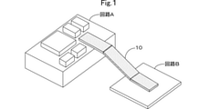
- FIG. 3 is an external perspective view of a high frequency signal transmission line 10 having a bent portion connecting two circuits. It is a side view of the high frequency signal transmission line 10 which has a bent part which connects two circuits.
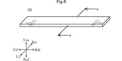
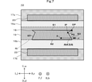
- FIG. 3 is an external perspective view of a high frequency signal transmission line 10 having a bent portion. It is an external perspective view of the high frequency signal transmission line 10 which is not bent. It is an exploded perspective view of the high frequency signal transmission line 10 which is not bent. It is sectional drawing in AA of FIG. It is sectional drawing of the high frequency signal transmission line 10 provided with the adhesive layer formed by an adhesive. It is sectional drawing in AA of the high frequency signal transmission line 10a which concerns on 1st modification.
- FIG. 1 is an external perspective view of a high frequency signal transmission line 10 having a bent portion connecting two circuits.
- FIG. 2 is a side view of a high frequency signal transmission line 10 having a bent portion connecting two circuits.
- FIG. 3 is an external perspective view of a high frequency signal transmission line 10 having a bent portion.
- FIG. 4 is an external perspective view of the high frequency signal transmission line 10 which is not bent.
- FIG. 5 is an exploded perspective view of the high frequency signal transmission line 10 which is not bent.
- FIG. 6 is a view of the cross section taken along the line AA shown in FIG. In addition, in FIG. 1 and FIG.
- the high frequency signal transmission line 10 is shown by a dot pattern. Further, in FIG. 2, parts other than the high-frequency signal transmission line 10 provided at the upper end of the circuit A are not shown. Further, in FIG. 3, the circuit to which the high frequency signal transmission line 10 is connected is not shown.
- the direction is defined as follows.
- the stacking direction of the prime field 15 of the high frequency signal transmission line 10 is defined as the vertical direction of the laminated body.
- the longitudinal direction of the prime field 15 is defined as the front-back direction of the laminated body.
- the lateral direction of the prime field 15 is defined as the left-right direction of the laminated body.
- the vertical direction of the laminated body, the front-rear direction of the laminated body, and the horizontal direction of the laminated body are orthogonal to each other.
- the definitions of the direction and the stacking direction in this specification are examples. Therefore, it is not necessary that the direction of the high frequency signal transmission line 10 in actual use and the direction in the present specification match.
- the high frequency signal transmission line 10 (corresponding to a resin multilayer board) is used for connecting two circuits in an electronic device such as a mobile phone, for example.
- the high frequency signal transmission line 10 has flexibility. Therefore, the high-frequency signal transmission line 10 can be used in an electronic device in a state of being bent in the vertical direction (plane direction). For example, as shown in FIGS. 1 and 2, the high-frequency signal transmission line 10 can connect the circuit A and the circuit B in a state of being bent in the vertical direction.
- the bent high-frequency signal transmission line 10 also has flexibility. Therefore, it is possible to further bend the high frequency signal transmission line 10 in a bent state.
- the high frequency signal transmission line 10 has non-curved sections A1 and A3 and curved sections A2 as shown in FIGS. 2 and 3.
- the non-curved sections A1 and A3 are sections in which the high-frequency signal transmission line 10 is not bent in the vertical direction.
- the curved section A2 is a section in which the high frequency signal transmission line 10 has a portion bent in the vertical direction.
- the non-curved section A1 is adjacent to the curved section A2.
- the non-curved section A1 is located to the left of the curved section A2.
- the non-curved section A3 is adjacent to the curved section A2.
- the non-curved section A3 is located to the right of the curved section A2.
- the vertical direction of the laminated body and the front-back direction of the laminated body differ depending on the position of the high-frequency signal transmission line 10 as shown in FIGS. 2 and 3.
- the vertical direction of the laminated body and the front-rear direction of the laminated body coincide with the vertical direction and the front-rear direction, respectively.
- the curved section A2 where the high frequency signal transmission line 10 is bent for example, the position of (2) in FIG. 2
- the vertical direction of the laminated body and the front-rear direction of the laminated body do not match the vertical direction and the front-back direction, respectively. ..
- the high frequency signal transmission line 10 is not bent. In this case, the high frequency signal transmission line 10 includes only an unbent non-curved section. Therefore, in the high-frequency signal transmission line 10 shown in FIGS. 4 and 5, the vertical direction of the laminated body and the front-rear direction of the laminated body coincide with the vertical direction and the front-rear direction, respectively. As shown in FIGS. 4 and 5, the high-frequency signal transmission line 10 includes a resin layer 16a (corresponding to an upper resin layer), a resin layer 16b (corresponding to a lower resin layer), and resist layers 17a and 17b (corresponding to a protective film).
- a resin layer 16a corresponding to an upper resin layer
- a resin layer 16b corresponding to a lower resin layer
- resist layers 17a and 17b corresponding to a protective film
- Signal conductor layer 18 (corresponding to metal foil layer), 1st ground conductor layer 20 (corresponding to metal foil layer), 2nd ground conductor layer 22 (corresponding to metal foil layer), external electrodes 24, 26, a plurality of first It includes one interlayer connecting conductor v1, a plurality of second interlayer connecting conductors v2, and interlayer connecting conductors v11 and v12.
- the resin layers 16a and 16b have a rectangular shape having long sides extending in the front-rear direction when viewed in the vertical direction. Therefore, the length of the resin layers 16a and 16b in the front-rear direction is longer than the length of the resin layers 16a and 16b in the left-right direction. The length of the resin layers 16a and 16b in the front-rear direction is longer than the length of the resin layers 16a and 16b in the vertical direction.
- the resin layers 16a and 16b have flexibility.
- the resin layers 16a and 16b are flexible dielectric sheets.
- the materials of the resin layers 16a and 16b are thermoplastic resins such as polyimide and liquid crystal polymers.
- Such resin layers 16a and 16b form the prime field 15. More specifically, the prime field 15 has a structure in which the resin layers 16a and 16b are laminated in the vertical direction. The resin layers 16a and 16b are laminated so as to be arranged in this order from top to bottom.
- the prime field 15 has a plate shape. As shown in FIG. 5, the prime field 15 has a rectangular shape having a long side extending in the front-rear direction when viewed in the vertical direction. Therefore, the length of the prime field 15 in the front-rear direction is longer than the length of the prime field 15 in the left-right direction. The length of the prime field 15 in the front-rear direction is longer than the length of the prime field 15 in the vertical direction.
- the signal conductor layer 18 is provided on the upper main surface of the resin layer 16b. As a result, the signal conductor layer 18 is provided in the prime field 15. As shown in FIG. 5, the signal conductor layer 18 has a linear shape extending in the front-rear direction. The signal conductor layer 18 is arranged at the center of the upper main surface of the resin layer 16b in the left-right direction. The front end of the signal conductor layer 18 is located at the front end of the resin layer 16b. The rear end of the signal conductor layer 18 is located at the rear end of the resin layer 16b. In the high frequency signal transmission line 10, the signal conductor layer 18 is formed of a metal foil layer. The signal conductor layer 18 is a kind of circuit pattern. Therefore, the circuit pattern is formed by the metal foil layer. A high frequency signal is transmitted to the signal conductor layer 18.
- the first ground conductor layer 20 is provided on the upper main surface of the resin layer 16a. As a result, the first ground conductor layer 20 is located above the signal conductor layer 18.
- the first ground conductor layer 20 is located above the signal conductor layer 18 in the vertical direction. At least a portion of the first ground conductor layer 20 is located within a region through which the signal conductor layer 18 translates upward. Therefore, the first ground conductor layer 20 may be contained in the region through which the signal conductor layer 18 passes when the signal conductor layer 18 moves in parallel, or protrudes from the region through which the signal conductor layer 18 passes when the signal conductor layer 18 moves in parallel. You may. In the present embodiment, the first ground conductor layer 20 protrudes from the region through which the signal conductor layer 18 passes when it is translated.
- the first ground conductor layer 20 has a rectangular shape having a long side extending in the front-rear direction when viewed in the vertical direction.
- the first ground conductor layer 20 has a shape that substantially matches the resin layer 16a when viewed in the vertical direction. However, the first ground conductor layer 20 is slightly smaller than the resin layer 16a when viewed in the vertical direction.
- a ground is connected to the first ground conductor layer 20.
- the second ground conductor layer 22 is provided on the lower main surface of the resin layer 16b. As a result, the second ground conductor layer 22 is located below the signal conductor layer 18. As shown in FIG. 5, the second ground conductor layer 22 has a rectangular shape having a long side extending in the front-rear direction when viewed in the vertical direction. The second ground conductor layer 22 has a shape that substantially matches the resin layer 16b when viewed in the vertical direction. However, the second ground conductor layer 22 is slightly smaller than the resin layer 16b when viewed in the vertical direction. A ground is connected to the second ground conductor layer 22. As described above, the first ground conductor layer 20 and the second ground conductor layer 22 have a stripline structure.
- the external electrode 24 is provided at the front end portion of the lower main surface of the resin layer 16b.
- the external electrode 24 has a rectangular shape when viewed in the vertical direction.
- the external electrode 24 overlaps the front end portion of the signal conductor layer 18 when viewed in the vertical direction.
- the second ground conductor layer 22 is not provided around the external electrode 24 so that the external electrode 24 is insulated from the second ground conductor layer 22.
- the external electrode 26 has a structure symmetrical to that of the external electrode 24. Therefore, the description of the external electrode 26 will be omitted.
- the signal conductor layer 18, the first ground conductor layer 20, the second ground conductor layer 22, and the external electrodes 24, 26 as described above are, for example, copper provided on the upper main surface or the lower main surface of the resin layers 16a and 16b. It is formed by etching the foil.
- the plurality of first interlayer connecting conductors v1 are provided on the prime field 15 so as to be located on the left side of the signal conductor layer 18.
- the plurality of first interlayer connection conductors v1 are arranged so as to be arranged in a line at equal intervals in the front-rear direction.
- the plurality of first interlayer connecting conductors v1 penetrate the resin layers 16a and 16b in the vertical direction.
- the upper ends of the plurality of first interlayer connecting conductors v1 are connected to the first ground conductor layer 20.
- the lower ends of the plurality of first interlayer connecting conductors v1 are connected to the second ground conductor layer 22.
- the plurality of first interlayer connecting conductors v1 electrically connect the first ground conductor layer 20 and the second ground conductor layer 22.
- the plurality of second interlayer connecting conductors v2 are provided on the prime field 15 so as to be located on the right side of the signal conductor layer 18.
- the plurality of second interlayer connecting conductors v2 are arranged so as to be arranged in a line at equal intervals in the front-rear direction.
- the plurality of second interlayer connecting conductors v2 penetrate the resin layers 16a and 16b in the vertical direction.
- the upper ends of the plurality of second interlayer connecting conductors v2 are connected to the first ground conductor layer 20.
- the lower ends of the plurality of second interlayer connecting conductors v2 are connected to the second ground conductor layer 22.
- the plurality of second interlayer connecting conductors v2 electrically connect the first ground conductor layer 20 and the second ground conductor layer 22.
- the interlayer connecting conductor v11 is provided at the front end of the prime field 15.
- the interlayer connecting conductor v11 penetrates the resin layer 16b in the vertical direction.
- the intermediate portion of the interlayer connection conductor v11 is connected to the front end portion of the signal conductor layer 18.
- the lower end of the interlayer connection conductor v11 is connected to the external electrode 24.
- the interlayer connection conductor v11 electrically connects the signal conductor layer 18 and the external electrode 24.
- the interlayer connecting conductor v12 has a structure symmetrical to that of the interlayer connecting conductor v11. Therefore, the description of the interlayer connection conductor v12 will be omitted.
- the interlayer connecting conductors v1, v2, v11, and v12 are through-hole conductors.
- the through-hole conductor is formed by plating the through holes formed in the resin layers 16a and 16b.
- the interlayer connection conductors v1, v2, v11, and v12 may be via hole conductors.
- the resist layers 17a and 17b have the same rectangular shape as the prime field 15 when viewed in the vertical direction.
- the resist layers 17a and 17b are not a part of the prime field 15.
- the materials of the resist layers 17a and 17b and the materials of the prime field 15 are different. That is, the resist layers 17a and 17b are layers different from the prime field 15.
- the resist layer 17a covers the surface of the prime field 15.
- the resist layer 17a is provided on the upper main surface of the prime field 15.
- the resist layer 17a is a protective film and covers the first ground conductor layer 20. As a result, the resist layer 17a protects the first ground conductor layer 20.
- a resist layer 17a is a resist, a coverlay, or the like.
- the resist layer 17a is a resist
- the upper main surface of the resin layer 16a is coated with the resist.
- the resist layer 17a is a coverlay, the resin layer 16a and the resist layer 17a are adhered to each other by an adhesive or the like (not shown).
- the resist layer 17b covers the surface of the prime field 15. Specifically, the resist layer 17b is provided below the lower main surface of the prime field 15. The resist layer 17b covers the second ground conductor layer 22. As a result, the resist layer 17b protects the second ground conductor layer 22. However, since the upper main surface of the second ground conductor layer 22 is fixed to the prime field 15, it is not covered by the resist layer 17b. Similar to the resist layer 17a, the resist layer 17b is a resist, a coverlay, or the like.
- the resist layer 17b is provided with openings h11 to h18. Looking downward at the resist layer 17b, the opening h11 overlaps with the external electrode 24. Looking downward at the resist layer 17b, the opening h15 overlaps with the external electrode 26. As a result, the external electrodes 24 and 26 are exposed to the outside from the high frequency signal transmission line 10 via the openings h11 and h15, respectively.
- the opening h12 is provided to the right of the opening h11.
- the opening h13 is provided in front of the opening h11.
- the opening h14 is provided to the left of the opening h11.
- the second ground conductor layer 22 is exposed to the outside from the high frequency signal transmission line 10 through the openings h12 to h14.
- the openings h16 to h18 have a structure symmetrical with the openings h12 to h14, respectively. Therefore, the description of the openings h16 to h18 will be omitted.
- the second ground conductor layer 22 is provided with openings h19 and h20.
- the size of the diameters of the openings h19 and h20 is larger than the size of the diameters of the external electrodes 24 and 26. Therefore, when viewed in the vertical direction, the external electrode 24 and the external electrode 26 do not inscribe the openings h19 and h20, respectively. As a result, the external electrodes 24 and 26 and the second ground conductor layer 22 are not short-circuited.
- the high frequency signal transmission line 10 has a structure that prevents the resin layer 16a and the resin layer 16b from peeling off. In the following, this structure will be described in more detail.
- the signal conductor layer 18 includes a signal conductor layer upper main surface S1 (metal foil layer upper main surface), a signal conductor layer lower main surface S2 (metal leaf layer lower main surface), and a signal conductor layer side surface S3. (Side surface of metal foil layer) is included.
- the main surface S1 on the signal conductor layer is a portion that can be visually recognized when the signal conductor layer 18 is viewed downward.
- the lower main surface S2 of the signal conductor layer is a portion that can be visually recognized by looking upward at the signal conductor layer 18.
- the side surface S3 of the signal conductor layer is a surface of the surface of the signal conductor layer 18 excluding the upper main surface S1 of the signal conductor layer and the lower main surface S2 of the signal conductor layer.
- the signal conductor layer 18 may have any shape as long as it is formed by the upper main surface S1 of the signal conductor layer, the lower main surface S2 of the signal conductor layer, and the side surface S3 of the signal conductor layer.
- the signal conductor layer 18 has a rectangular shape formed by one signal conductor layer upper main surface S1, one signal conductor layer lower main surface S2, and four signal conductor layer side surfaces S3. is doing.
- the lower main surface S2 of the signal conductor layer 18 is in contact with the resin layer 16b. More precisely, the lower main surface S2 of the signal conductor layer of the signal conductor layer 18 is in contact with the upper main surface of the resin layer 16b. The lower main surface S2 of the signal conductor layer of the signal conductor layer 18 is roughened. Therefore, it is possible to prevent the signal conductor layer 18 from peeling off from the lower main surface S2 of the signal conductor layer and the resin layer 16b. Further, the main surface S1 on the signal conductor layer of the signal conductor layer 18 is in contact with the resin layer 16a. More precisely, the signal conductor layer upper main surface S1 of the signal conductor layer 18 is in contact with the lower main surface of the resin layer 16a.
- the upper main surface of the signal conductor layer 18 is not roughened in order to prevent an increase in transmission loss of an electric signal. Therefore, the resin layer 16a is not fixed to the signal conductor layer 18. As a result, the adhesion strength of the signal conductor layer 18 to the resin layer 16b is stronger than the adhesion strength of the signal conductor layer 18 to the resin layer 16a.
- the signal conductor layer 18 is provided between the resin layer 16a and the resin layer 16b. Therefore, the resin layer 16a and the resin layer 16b do not come into contact with each other on the entire surface of the lower main surface of the resin layer 16a and the entire surface of the upper main surface of the resin layer 16b. Therefore, a part of the lower main surface of the resin layer 16a is in contact with a part of the upper main surface of the resin layer 16b. As a result, the layer interface RI between the resin layer 16a and the resin layer 16b is formed. The layer interface RI is formed at a portion where the lower main surface of the resin layer 16a and the upper main surface of the resin layer 16b are in contact with each other. Therefore, the layer interface RI is not formed in the portion where the signal conductor layer 18 is provided.
- the shape of the side surface of the signal conductor layer 18 will be described in more detail. In the following, attention will be paid to the right side surface of the signal conductor layer 18.
- the signal conductor layer 18 is formed from the inside of the region surrounded by the surface of the signal conductor layer 18 in the direction orthogonal to the vertical direction of the laminated body.
- the direction toward the outside of the area surrounded by the surface is defined as the inside-out direction.
- a point located inside a region surrounded by the surface of the signal conductor layer 18 in a cross section parallel to the vertical direction of the laminated body is defined as a point X.
- a point located outside the region surrounded by the surface of the signal conductor layer 18 is defined as a point Y.
- the position of the point X in the vertical direction of the laminated body and the position of the point Y in the vertical direction of the laminated body are the same.
- the inside / outside direction is the direction from the point X to the point Y (see FIG. 6).
- the inside / outside direction is the right direction.
- the side surface of the signal conductor layer 18 has a cross-sectional shape in which the V shape is rotated by 90 °.
- the side surface of the signal conductor layer 18 is a slope extending outward and upward from the center of the side surface of the signal conductor layer 18 in the vertical direction of the laminate, and the center of the side surface of the signal conductor layer 18 in the vertical direction of the laminate. It has a slope that extends outward and downward from.
- the signal conductor layer 18 has a structure described below because the side surface of the signal conductor layer 18 has a slope extending outward and upward from the center in the vertical direction of the laminate on the side surface of the signal conductor layer 18. Have.
- the side surface of the signal conductor layer 18 has an outer portion OP and an inner portion IP in a cross section parallel to the vertical direction of the laminated body.
- the outer portion OP is located at a portion where the resin layer 16a comes into contact with the side surface.
- the right side surface of the signal conductor layer 18 has an outer portion OP in a cross section perpendicular to the front-rear direction.
- the side surface of the signal conductor layer 18 has an inner portion IP in a cross section parallel to the vertical direction of the laminated body.
- the inner portion IP is located at a portion where the resin layer 16a comes into contact with the side surface.
- the inner location IP is located below the outer location OP and inside the outer location OP in the inner and outer directions.
- the inside / outside direction is the right direction. Therefore, the right side surface of the signal conductor layer 18 has an inner portion IP located below the outer portion OP and located to the left in the cross section perpendicular to the front-rear direction.
- the outer portion OP and the inner portion IP are located on the side surface of the signal conductor layer 18 and the portion where the resin layer 16a contacts. Therefore, the outer portion OP and the inner portion IP are not located at the portion where the side surface of the signal conductor layer 18 and the resin layer 16b are in contact with each other. In other words, below the layer interface RI, the outer location OP and the inner location IP are not located. Since the left side surface of the signal conductor layer 18 has a structure symmetrical to the right side surface of the signal conductor layer 18, the description thereof will be omitted.
- the resin layer 16a is suppressed from being peeled from the resin layer 16b.
- the side surface of the signal conductor layer 18 is an outer portion OP and an inner side located at a portion where the resin layer 16a contacts the side surface of the signal conductor layer 18 in a cross section parallel to the vertical direction of the laminate of the signal conductor layer 18. It has a location IP.
- the inner portion IP is located below the outer portion OP and is located inside the outer portion OP in the inner / outer direction. Therefore, the resin layer 16a is located under the portion P0 between the outer portion OP and the inner portion IP on the side surface of the signal conductor layer 18.
- the resin layer 16a is caught by the portion P0. This prevents the resin layer 16a from peeling off from the signal conductor layer 18. As a result, the resin layer 16a is suppressed from being peeled from the resin layer 16b due to the resin layer 16a being peeled from the signal conductor layer 18.
- the signal conductor layer 18 is roughened only on the lower main surface, it is possible to suppress an increase in transmission loss of an electric signal.
- a resin layer 16a having a metal foil layer attached to the upper main surface and a resin layer 16b having a metal foil layer attached to the upper main surface and the lower main surface are prepared.
- the first ground conductor layer 20 is formed by etching the metal foil layer attached to the upper main surface of the resin layer 16a.
- the signal conductor layer 18, the second ground conductor layer 22, and the external electrodes 24, 26 are formed by etching the metal foil layer attached to the upper main surface and the lower main surface of the resin layer 16b.
- a mask having the same shape as the first ground conductor layer 20 is formed on the metal foil layer attached to the upper main surface of the resin layer 16a, and the metal foil layer on which the mask is formed is etched. ..
- the first ground conductor layer 20 is formed.
- the metal foil layer attached to the upper main surface and the lower main surface of the resin layer 16b is etched to form the signal conductor layer 18, the second ground conductor layer 22, and the external electrodes 24 and 26.
- the third step by deforming and processing the signal conductor layer 18, it is located below and inside the outermost OP and the outer OP in the inner and outer directions. It forms the side surface of the signal conductor layer 18 with an inner location IP.
- the third step is, for example, a wet blasting method.
- the resin layer 16a is laminated on the signal conductor layer 18 and the resin layer 16b. Specifically, the resin layer 16a is heat-pressed from above the signal conductor layer 18 and the resin layer 16b.
- the resin layer 16a is a thermoplastic resin (for example, a liquid crystal polymer). Therefore, the resin layer 16a softens and flows during the heating press. The flowed resin layer 16a enters below the portion P0 between the outer portion OP and the inner portion IP. Then, the temperature of the resin layer 16a that has entered under the portion P0 returns to room temperature and solidifies. At this time, the solidified resin layer 16a is caught on the portion P0. Therefore, peeling of the resin layer 16a from the resin layer 16b is suppressed.
- a thermoplastic resin for example, a liquid crystal polymer
- the high frequency signal transmission line 10 may be provided with an adhesive layer between the resin layer 16a and the resin layer 16b.
- an adhesive layer 19 formed of an adhesive is laminated on the signal conductor layer 18 and the resin layer 16b. You may.
- the adhesive layer 19 is formed of a material that solidifies at a temperature lower than the melting point of the resin layer 16b.
- the adhesive layer 19 is, for example, a thermoplastic material such as LCP or a fluororesin having a melting point lower than that of the resin layer 16b.
- the adhesive layer 19 is, for example, a thermosetting material such as an elastomer material or an epoxy resin having high fluidity even at a temperature lower than the melting point of the resin layer 16b.
- the resin layer 16a is laminated on the adhesive layer 19.
- the adhesive layer 19 corresponds to the upper resin layer.
- the resin layer 16b fixed to the signal conductor layer 18 may flow and change its shape at the time of hot pressing as well as the resin layer 16a.
- the resin layer 16b flows and the shape changes, the electrical characteristics of the high-frequency signal transmission line 10 may change.
- the adhesive layer 19 solidifies at a temperature lower than the melting point of the resin layer 16b. Therefore, by performing the heating press at a temperature at which the resin layer 16b does not flow and the adhesive layer 19 flows, the possibility that the shape of the resin layer 16b changes can be reduced.
- the adhesive layer 19 is used as compared with the case where the resin layer 16a is used, it is possible to form the high frequency signal transmission line 10 while reducing the possibility that the electrical characteristics change.
- the resin layers 16a and 16b are irradiated with a laser beam to form through holes. Then, by forming the conductor in the through hole by the plating process, the interlayer connection conductors v1, v2, v11, and v12 are formed.
- the through hole may be formed by a drill.
- the openings h11 to h18 and the resist layers 17a and 17b are formed. Through the above steps, the high frequency signal transmission line 10 is completed.
- the high frequency signal transmission line 10 can be easily manufactured. More specifically, by laminating the resin layer 16a on the signal conductor layer 18 and the resin layer 16b formed in the second step, the outer portion OP is formed under the side surface of the signal conductor layer 18. , At least a part of the resin layer 16b enters. As a result, the high frequency signal transmission line 10 can be easily manufactured.
- the outer portion OP and the inner portion IP can be easily formed on all the side surfaces of the signal conductor layer 18. More specifically, the upper main surface of the signal conductor layer 18 is crushed by the wet blasting method. When the upper main surface of the signal conductor layer 18 is crushed, the side surface of the signal conductor layer 18 protrudes in the inward and outward directions, and an outer portion OP and an inner portion IP can be formed on all the side surfaces of the signal conductor layer 18.
- FIG. 8 is a cross-sectional view taken along the line AA of the high frequency signal transmission line 10a.
- FIG. 4 is incorporated.
- the high frequency signal transmission line 10a is different from the high frequency signal transmission line 10 in that the shape of the signal conductor layer 18a is different from the shape of the signal conductor layer 18. Since the other configurations of the high frequency signal transmission line 10a are the same as those of the high frequency signal transmission line 10, the description thereof will be omitted.
- the side surface of the signal conductor layer 18a has a cross-sectional shape that can be defined by a single diagonal line. Specifically, the side surface of the signal conductor layer 18a is located below the outer portion OP1 from the outer portion OP1 located at the upper end of the side surface of the signal conductor layer 18 in the vertical direction of the laminate, and is located above the outer portion OP1. Also has a slope that extends straight to the inner location IP1 located inside. In this case, the resin layer 16a is located under the portion P1 between the outer portion OP1 and the inner portion IP1 on the side surface of the signal conductor layer 18a. Therefore, the resin layer 16a is caught on the portion P1. This prevents the resin layer 16a from peeling off from the resin layer 16b.
- FIG. 9 is a cross-sectional view taken along the line AA of the high frequency signal transmission line 10b.
- FIG. 10 is a cross-sectional view taken along the line AA of the high frequency signal transmission line 10b2.
- FIG. 4 is incorporated.
- the high frequency signal transmission line 10b is different from the high frequency signal transmission line 10 in that the shape of the signal conductor layer 18b is different from the shape of the signal conductor layer 18. Since the other configurations of the high frequency signal transmission line 10c are the same as those of the high frequency signal transmission line 10, the description thereof will be omitted.
- a protrusion protruding outward is formed near the center of the right side surface of the signal conductor layer 18b.
- the outer portion OP2 is located on the protrusion.
- the inner portion IP2 is located at the location where the right side surface of the signal conductor layer 18b and the layer interface RI are in contact with each other.
- the resin layer 16a is located under the portion P2 between the outer portion OP2 and the inner portion IP2. Therefore, the resin layer 16b is caught on the protrusion. This prevents the resin layer 16a from peeling off from the resin layer 16b.
- the shape of the protrusion may be any shape. Further, the protrusions do not necessarily have to extend in a direction parallel to the left-right direction of the laminated body. In the example shown in FIG. 9, the protrusion has a rectangular shape extending toward the right side of the laminated body. However, as shown in FIG. 10, the protrusion may have a triangular prism shape extending toward the right side of the laminated body. In this case, as shown in FIG. 10, the protrusions have a triangular shape when viewed in the front-rear direction. Specifically, the protrusion has a first surface SS1 and a second surface SS2. The first surface SS1 is located above the second surface SS2.
- the second surface SS2 extends in the inward and outward directions when viewed in the front-rear direction.
- the first surface SS1 extends in the inward / outward direction and in the downward direction of the laminated body when viewed in the front-rear direction. Then, when viewed in the front-rear direction, the first surface SS1 and the second surface SS2 are in contact with each other at the outer portion OP2. Even in this case, the resin layer 16a is located under the portion P2 between the outer portion OP2 and the inner portion IP2. Therefore, peeling of the resin layer 16a from the resin layer 16b is suppressed.
- FIG. 11 is a cross-sectional view taken along the line AA of the high frequency signal transmission line 10c.
- FIG. 4 is incorporated.
- the shape of the first ground conductor layer 20b is different from the shape of the first ground conductor layer 20, and the shape of the second ground conductor layer 22b is the second ground conductor. It differs from the high frequency signal transmission line 10 in that it differs from the layer 22. Since the other configurations of the high frequency signal transmission line 10c are the same as those of the high frequency signal transmission line 10, the description thereof will be omitted.
- the side surface of the first ground conductor layer 20b includes an outer portion OP3 located on the outermost side of the portion where the resist layer 17a contacts the side surface in the inner and outer directions. Further, the side surface of the first ground conductor layer 20b is an inner portion IP3 located below the outer portion OP3 and inside the outer portion OP3 in the portion where the resist layer 17a contacts the side surface in the inner and outer directions. Has. The resist layer 17a is located under the portion P3 between the outer portion OP3 and the inner portion IP3 on the side surface of the first ground conductor layer 20b. Therefore, the resist layer 17a is caught on the portion P3. This prevents the resist layer 17a from peeling off from the resin layer 16a. In this case, the first ground conductor layer 20b corresponds to the metal foil layer, the resist layer 17a corresponds to the upper resin layer, and the resin layer 16a corresponds to the lower resin layer.
- the second ground conductor layer 22b corresponds to the metal foil layer
- the resist layer 17b corresponds to the upper resin layer
- the resin layer 16b corresponds to the lower resin layer. .. Therefore, peeling of the resist layer 17b from the resin layer 16b is suppressed.
- the high frequency signal transmission line 10c includes a plurality of sets of the upper resin layer, the lower resin layer, and the metal foil layer. More specifically, the high frequency signal transmission line 10c includes three sets of an upper resin layer, a lower resin layer, and a metal foil layer.
- FIG. 12 is a cross-sectional view taken along the line AA of the high frequency signal transmission line 10d.
- the high-frequency signal transmission line 10d differs from the high-frequency signal transmission line 10 in that it includes a signal conductor layer 18d having a shape different from that of the signal conductor layer 18. Since the other configurations of the high frequency signal transmission line 10d are the same as those of the high frequency signal transmission line 10, the description thereof will be omitted.
- the shape of the side surface of the signal conductor layer 18d is different from the shape of the side surface of the signal conductor layer 18.
- the portion of the side surface of the signal guide layer 18d located below the inner portion IP4 is parallel to the vertical direction of the laminated body.
- the resin layer 16a is located under the portion P4 in the same manner as in the high frequency signal transmission line 10 (see FIG. 12). Therefore, in the high frequency signal transmission line 10d, the resin layer 16a is suppressed from peeling from the resin layer 16b for the same reason as the high frequency signal transmission line 10.
- the resin layer 16a is separated from the resin layer 16b regardless of the shape of the side surface of the signal guide layer 18d located below the inner portion IP4. Peeling is suppressed.
- the materials of the resin layer 16a and the resin layer 16b do not necessarily have to be the same, but may be different.
- the outer portions OP, OP2, OP3, and OP4 are not necessarily in the vertical direction of the laminate on the side surfaces of the signal conductor layers 18a and 18b and the first ground conductor layer 20b. It does not have to be above the center of. Further, in the high frequency signal transmission lines 10, 10b, 10b2, 10c, and 10d, the inner portions IP, IP2, IP3, and IP4 are not necessarily in the vertical direction of the laminate on the side surfaces of the signal conductor layers 18a and 18b and the first ground conductor layer 20b. It does not have to be located below the center of.
- the outer portions OP, OP2, OP3 and OP4 are laminated with the side surfaces of the signal conductor layers 18a and 18b and the first ground conductor layer 20b. It is located above the center in the vertical direction of the body, and the inner portions IP, IP, IP2, IP3, and IP4 may be located below the center in the vertical direction of the laminated body on the side surface.
- the resin layers 16a and 16b do not have to be thermoplastic resins.
- the signal conductor layer 18 may be fixed to the resin layer 16a.
- all the side surfaces of the signal conductor layer 18 may be provided with the outer portion OP, OP1 to OP4, and the inner portion IP, IP1 to IP4.
- the outer portions OP, OP1 to OP4 are located above the inner portions IP, IP1 to IP4, and the layer interface RI in all the cross sections of the signal conductor layer 18 parallel to the vertical direction of the laminate.
- a part of the side surface of the signal conductor layer 18 may be provided with an outer portion OP, OP1 to OP4 and an inner portion IP, IP1 to IP4.
- the left side surface of the signal conductor layer 18 may have a structure asymmetrical with the right side surface of the signal conductor layer 18.
- the left side surface of the signal conductor layer 18d may have a structure asymmetrical with the right side surface of the signal conductor layer 18d.
- the left side surface of the first ground conductor layer 20b may have a structure asymmetrical with the right side surface of the first ground conductor layer 20b.
- the left side surface of the second ground conductor layer 22b may have a left-right asymmetrical structure with the right side surface of the second ground conductor layer 22b.
Landscapes
- Engineering & Computer Science (AREA)
- Mechanical Engineering (AREA)
- Microelectronics & Electronic Packaging (AREA)
- Production Of Multi-Layered Print Wiring Board (AREA)
- Structure Of Printed Boards (AREA)
- Manufacturing Of Printed Wiring (AREA)
Priority Applications (3)
| Application Number | Priority Date | Filing Date | Title |
|---|---|---|---|
| JP2022537928A JP7456504B2 (ja) | 2020-07-21 | 2021-07-12 | 樹脂多層基板および樹脂多層基板の製造方法 |
| CN202190000713.1U CN219697975U (zh) | 2020-07-21 | 2021-07-12 | 树脂多层基板 |
| US18/096,620 US12403673B2 (en) | 2020-07-21 | 2023-01-13 | Resin multilayer substrate and method for manufacturing resin multilayer substrate |
Applications Claiming Priority (2)
| Application Number | Priority Date | Filing Date | Title |
|---|---|---|---|
| JP2020124365 | 2020-07-21 | ||
| JP2020-124365 | 2020-07-21 |
Related Child Applications (1)
| Application Number | Title | Priority Date | Filing Date |
|---|---|---|---|
| US18/096,620 Continuation US12403673B2 (en) | 2020-07-21 | 2023-01-13 | Resin multilayer substrate and method for manufacturing resin multilayer substrate |
Publications (1)
| Publication Number | Publication Date |
|---|---|
| WO2022019156A1 true WO2022019156A1 (ja) | 2022-01-27 |
Family
ID=79728749
Family Applications (1)
| Application Number | Title | Priority Date | Filing Date |
|---|---|---|---|
| PCT/JP2021/026064 Ceased WO2022019156A1 (ja) | 2020-07-21 | 2021-07-12 | 樹脂多層基板および樹脂多層基板の製造方法 |
Country Status (4)
| Country | Link |
|---|---|
| US (1) | US12403673B2 (https=) |
| JP (1) | JP7456504B2 (https=) |
| CN (1) | CN219697975U (https=) |
| WO (1) | WO2022019156A1 (https=) |
Citations (5)
| Publication number | Priority date | Publication date | Assignee | Title |
|---|---|---|---|---|
| JPS6482595A (en) * | 1987-09-25 | 1989-03-28 | Meiko Electronics Co Ltd | Printed wiring board |
| WO2011007659A1 (ja) * | 2009-07-13 | 2011-01-20 | 株式会社村田製作所 | 信号線路及びその製造方法 |
| JP2013041858A (ja) * | 2011-08-11 | 2013-02-28 | Fujikura Ltd | プリント配線板 |
| WO2018155014A1 (ja) * | 2017-02-23 | 2018-08-30 | 日本碍子株式会社 | 絶縁放熱基板 |
| WO2019107430A1 (ja) * | 2017-11-29 | 2019-06-06 | 京セラ株式会社 | 回路基板およびこれを備える発光装置 |
Family Cites Families (10)
| Publication number | Priority date | Publication date | Assignee | Title |
|---|---|---|---|---|
| JP3069476B2 (ja) | 1993-01-26 | 2000-07-24 | イビデン株式会社 | 多層プリント配線板およびその製造方法 |
| JP4433814B2 (ja) * | 2004-02-06 | 2010-03-17 | 凸版印刷株式会社 | 微細加工製品及びその製造方法 |
| JP2006019321A (ja) * | 2004-06-30 | 2006-01-19 | Toray Eng Co Ltd | 回路基板及びその製造方法 |
| JP2007317900A (ja) | 2006-05-26 | 2007-12-06 | Nitto Denko Corp | 配線回路基板およびその製造方法 |
| JP5354018B2 (ja) | 2009-08-11 | 2013-11-27 | 株式会社村田製作所 | 多層基板 |
| CN204559998U (zh) * | 2012-12-12 | 2015-08-12 | 株式会社村田制作所 | 柔性基板及电子设备 |
| JP5983523B2 (ja) | 2013-05-06 | 2016-08-31 | 株式会社デンソー | 多層基板およびこれを用いた電子装置、電子装置の製造方法 |
| JP6322492B2 (ja) * | 2014-06-16 | 2018-05-09 | 日本シイエムケイ株式会社 | プリント配線板および、その製造方法 |
| JP2016066705A (ja) * | 2014-09-25 | 2016-04-28 | イビデン株式会社 | プリント配線板およびその製造方法 |
| JP7424802B2 (ja) * | 2019-11-12 | 2024-01-30 | 日東電工株式会社 | 配線回路基板およびその製造方法 |
-
2021
- 2021-07-12 WO PCT/JP2021/026064 patent/WO2022019156A1/ja not_active Ceased
- 2021-07-12 CN CN202190000713.1U patent/CN219697975U/zh active Active
- 2021-07-12 JP JP2022537928A patent/JP7456504B2/ja active Active
-
2023
- 2023-01-13 US US18/096,620 patent/US12403673B2/en active Active
Patent Citations (5)
| Publication number | Priority date | Publication date | Assignee | Title |
|---|---|---|---|---|
| JPS6482595A (en) * | 1987-09-25 | 1989-03-28 | Meiko Electronics Co Ltd | Printed wiring board |
| WO2011007659A1 (ja) * | 2009-07-13 | 2011-01-20 | 株式会社村田製作所 | 信号線路及びその製造方法 |
| JP2013041858A (ja) * | 2011-08-11 | 2013-02-28 | Fujikura Ltd | プリント配線板 |
| WO2018155014A1 (ja) * | 2017-02-23 | 2018-08-30 | 日本碍子株式会社 | 絶縁放熱基板 |
| WO2019107430A1 (ja) * | 2017-11-29 | 2019-06-06 | 京セラ株式会社 | 回路基板およびこれを備える発光装置 |
Also Published As
| Publication number | Publication date |
|---|---|
| CN219697975U (zh) | 2023-09-15 |
| US20230158775A1 (en) | 2023-05-25 |
| US12403673B2 (en) | 2025-09-02 |
| JP7456504B2 (ja) | 2024-03-27 |
| JPWO2022019156A1 (https=) | 2022-01-27 |
Similar Documents
| Publication | Publication Date | Title |
|---|---|---|
| JP5737328B2 (ja) | 電子機器 | |
| US9401534B2 (en) | High-frequency signal line and electronic device | |
| US11558958B2 (en) | Laminated body and method for manufacturing the same | |
| US9673501B2 (en) | Laminated flat cable and method for producing same | |
| US9130251B2 (en) | Flat cable | |
| KR20070108258A (ko) | 프린트 배선판 | |
| JP2012243923A (ja) | フレキシブルプリント回路及びその製造方法 | |
| US9871281B2 (en) | High-frequency signal line | |
| US9312590B2 (en) | High-frequency signal transmission line and electronic device | |
| US6545227B2 (en) | Pocket mounted chip having microstrip line | |
| WO2022019156A1 (ja) | 樹脂多層基板および樹脂多層基板の製造方法 | |
| US9583809B2 (en) | High-frequency signal line | |
| US12431603B2 (en) | Multilayer substrate and manufacturing method therefor | |
| JP2013026322A (ja) | プリント配線板 | |
| WO2020162473A1 (ja) | 樹脂多層基板および樹脂多層基板の製造方法 | |
| WO2023135931A1 (ja) | 多層基板 | |
| WO2022113618A1 (ja) | 伝送線路及び電子機器 | |
| US20150116060A1 (en) | High-frequency signal transmission line and electronic device | |
| WO2021006076A1 (ja) | 多層基板 | |
| CN218514588U (zh) | 内埋弹性连接件的电路板组件 | |
| US11716811B2 (en) | Printed wiring board | |
| WO2014065172A1 (ja) | フレキシブル基板 | |
| WO2022270294A1 (ja) | 多層基板、多層基板モジュール及び電子機器 | |
| JP2022162293A (ja) | 回路基板及び電子機器 | |
| JP2014078836A (ja) | 高周波信号線路及びその製造方法 |
Legal Events
| Date | Code | Title | Description |
|---|---|---|---|
| 121 | Ep: the epo has been informed by wipo that ep was designated in this application |
Ref document number: 21845630 Country of ref document: EP Kind code of ref document: A1 |
|
| ENP | Entry into the national phase |
Ref document number: 2022537928 Country of ref document: JP Kind code of ref document: A |
|
| WWE | Wipo information: entry into national phase |
Ref document number: 202190000713.1 Country of ref document: CN |
|
| NENP | Non-entry into the national phase |
Ref country code: DE |
|
| 122 | Ep: pct application non-entry in european phase |
Ref document number: 21845630 Country of ref document: EP Kind code of ref document: A1 |