WO2022013676A1 - 半導体装置、及び電子機器 - Google Patents
半導体装置、及び電子機器 Download PDFInfo
- Publication number
- WO2022013676A1 WO2022013676A1 PCT/IB2021/055988 IB2021055988W WO2022013676A1 WO 2022013676 A1 WO2022013676 A1 WO 2022013676A1 IB 2021055988 W IB2021055988 W IB 2021055988W WO 2022013676 A1 WO2022013676 A1 WO 2022013676A1
- Authority
- WO
- WIPO (PCT)
- Prior art keywords
- circuit
- transistor
- wiring
- terminal
- switch
- Prior art date
- Legal status (The legal status is an assumption and is not a legal conclusion. Google has not performed a legal analysis and makes no representation as to the accuracy of the status listed.)
- Ceased
Links
Images


Classifications
-
- H—ELECTRICITY
- H10—SEMICONDUCTOR DEVICES; ELECTRIC SOLID-STATE DEVICES NOT OTHERWISE PROVIDED FOR
- H10D—INORGANIC ELECTRIC SEMICONDUCTOR DEVICES
- H10D88/00—Three-dimensional [3D] integrated devices
-
- G—PHYSICS
- G06—COMPUTING OR CALCULATING; COUNTING
- G06N—COMPUTING ARRANGEMENTS BASED ON SPECIFIC COMPUTATIONAL MODELS
- G06N3/00—Computing arrangements based on biological models
- G06N3/02—Neural networks
- G06N3/06—Physical realisation, i.e. hardware implementation of neural networks, neurons or parts of neurons
- G06N3/063—Physical realisation, i.e. hardware implementation of neural networks, neurons or parts of neurons using electronic means
- G06N3/065—Analogue means
-
- G—PHYSICS
- G11—INFORMATION STORAGE
- G11C—STATIC STORES
- G11C11/00—Digital stores characterised by the use of particular electric or magnetic storage elements; Storage elements therefor
- G11C11/56—Digital stores characterised by the use of particular electric or magnetic storage elements; Storage elements therefor using storage elements with more than two stable states represented by steps, e.g. of voltage, current, phase, frequency
- G11C11/5621—Digital stores characterised by the use of particular electric or magnetic storage elements; Storage elements therefor using storage elements with more than two stable states represented by steps, e.g. of voltage, current, phase, frequency using charge storage in a floating gate
- G11C11/5642—Sensing or reading circuits; Data output circuits
-
- G—PHYSICS
- G06—COMPUTING OR CALCULATING; COUNTING
- G06G—ANALOGUE COMPUTERS
- G06G7/00—Devices in which the computing operation is performed by varying electric or magnetic quantities
- G06G7/48—Analogue computers for specific processes, systems or devices, e.g. simulators
- G06G7/60—Analogue computers for specific processes, systems or devices, e.g. simulators for living beings, e.g. their nervous systems ; for problems in the medical field
-
- G—PHYSICS
- G06—COMPUTING OR CALCULATING; COUNTING
- G06N—COMPUTING ARRANGEMENTS BASED ON SPECIFIC COMPUTATIONAL MODELS
- G06N3/00—Computing arrangements based on biological models
- G06N3/02—Neural networks
- G06N3/04—Architecture, e.g. interconnection topology
- G06N3/0464—Convolutional networks [CNN, ConvNet]
-
- G—PHYSICS
- G06—COMPUTING OR CALCULATING; COUNTING
- G06N—COMPUTING ARRANGEMENTS BASED ON SPECIFIC COMPUTATIONAL MODELS
- G06N3/00—Computing arrangements based on biological models
- G06N3/02—Neural networks
- G06N3/04—Architecture, e.g. interconnection topology
- G06N3/048—Activation functions
-
- G—PHYSICS
- G11—INFORMATION STORAGE
- G11C—STATIC STORES
- G11C11/00—Digital stores characterised by the use of particular electric or magnetic storage elements; Storage elements therefor
- G11C11/54—Digital stores characterised by the use of particular electric or magnetic storage elements; Storage elements therefor using elements simulating biological cells, e.g. neuron
-
- G—PHYSICS
- G11—INFORMATION STORAGE
- G11C—STATIC STORES
- G11C16/00—Erasable programmable read-only memories
- G11C16/02—Erasable programmable read-only memories electrically programmable
- G11C16/04—Erasable programmable read-only memories electrically programmable using variable threshold transistors, e.g. FAMOS
- G11C16/0408—Erasable programmable read-only memories electrically programmable using variable threshold transistors, e.g. FAMOS comprising cells containing floating gate transistors
- G11C16/0441—Erasable programmable read-only memories electrically programmable using variable threshold transistors, e.g. FAMOS comprising cells containing floating gate transistors comprising cells containing multiple floating gate devices, e.g. separate read-and-write FAMOS transistors with connected floating gates
-
- G—PHYSICS
- G11—INFORMATION STORAGE
- G11C—STATIC STORES
- G11C7/00—Arrangements for writing information into, or reading information out from, a digital store
- G11C7/06—Sense amplifiers; Associated circuits, e.g. timing or triggering circuits
-
- H—ELECTRICITY
- H10—SEMICONDUCTOR DEVICES; ELECTRIC SOLID-STATE DEVICES NOT OTHERWISE PROVIDED FOR
- H10B—ELECTRONIC MEMORY DEVICES
- H10B12/00—Dynamic random access memory [DRAM] devices
- H10B12/30—DRAM devices comprising one-transistor - one-capacitor [1T-1C] memory cells
-
- H—ELECTRICITY
- H10—SEMICONDUCTOR DEVICES; ELECTRIC SOLID-STATE DEVICES NOT OTHERWISE PROVIDED FOR
- H10B—ELECTRONIC MEMORY DEVICES
- H10B20/00—Read-only memory [ROM] devices
- H10B20/20—Programmable ROM [PROM] devices comprising field-effect components
-
- H—ELECTRICITY
- H10—SEMICONDUCTOR DEVICES; ELECTRIC SOLID-STATE DEVICES NOT OTHERWISE PROVIDED FOR
- H10D—INORGANIC ELECTRIC SEMICONDUCTOR DEVICES
- H10D30/00—Field-effect transistors [FET]
- H10D30/60—Insulated-gate field-effect transistors [IGFET]
- H10D30/67—Thin-film transistors [TFT]
-
- H—ELECTRICITY
- H10—SEMICONDUCTOR DEVICES; ELECTRIC SOLID-STATE DEVICES NOT OTHERWISE PROVIDED FOR
- H10D—INORGANIC ELECTRIC SEMICONDUCTOR DEVICES
- H10D84/00—Integrated devices formed in or on semiconductor substrates that comprise only semiconducting layers, e.g. on Si wafers or on GaAs-on-Si wafers
- H10D84/01—Manufacture or treatment
- H10D84/02—Manufacture or treatment characterised by using material-based technologies
- H10D84/03—Manufacture or treatment characterised by using material-based technologies using Group IV technology, e.g. silicon technology or silicon-carbide [SiC] technology
- H10D84/038—Manufacture or treatment characterised by using material-based technologies using Group IV technology, e.g. silicon technology or silicon-carbide [SiC] technology using silicon technology, e.g. SiGe
-
- H—ELECTRICITY
- H10—SEMICONDUCTOR DEVICES; ELECTRIC SOLID-STATE DEVICES NOT OTHERWISE PROVIDED FOR
- H10D—INORGANIC ELECTRIC SEMICONDUCTOR DEVICES
- H10D84/00—Integrated devices formed in or on semiconductor substrates that comprise only semiconducting layers, e.g. on Si wafers or on GaAs-on-Si wafers
- H10D84/80—Integrated devices formed in or on semiconductor substrates that comprise only semiconducting layers, e.g. on Si wafers or on GaAs-on-Si wafers characterised by the integration of at least one component covered by groups H10D12/00 or H10D30/00, e.g. integration of IGFETs
- H10D84/811—Combinations of field-effect devices and one or more diodes, capacitors or resistors
-
- H—ELECTRICITY
- H10—SEMICONDUCTOR DEVICES; ELECTRIC SOLID-STATE DEVICES NOT OTHERWISE PROVIDED FOR
- H10D—INORGANIC ELECTRIC SEMICONDUCTOR DEVICES
- H10D84/00—Integrated devices formed in or on semiconductor substrates that comprise only semiconducting layers, e.g. on Si wafers or on GaAs-on-Si wafers
- H10D84/80—Integrated devices formed in or on semiconductor substrates that comprise only semiconducting layers, e.g. on Si wafers or on GaAs-on-Si wafers characterised by the integration of at least one component covered by groups H10D12/00 or H10D30/00, e.g. integration of IGFETs
- H10D84/82—Integrated devices formed in or on semiconductor substrates that comprise only semiconducting layers, e.g. on Si wafers or on GaAs-on-Si wafers characterised by the integration of at least one component covered by groups H10D12/00 or H10D30/00, e.g. integration of IGFETs of only field-effect components
- H10D84/83—Integrated devices formed in or on semiconductor substrates that comprise only semiconducting layers, e.g. on Si wafers or on GaAs-on-Si wafers characterised by the integration of at least one component covered by groups H10D12/00 or H10D30/00, e.g. integration of IGFETs of only field-effect components of only insulated-gate FETs [IGFET]
- H10D84/85—Complementary IGFETs, e.g. CMOS
- H10D84/856—Complementary IGFETs, e.g. CMOS the complementary IGFETs having different architectures than each other, e.g. high-voltage and low-voltage CMOS
-
- H—ELECTRICITY
- H10—SEMICONDUCTOR DEVICES; ELECTRIC SOLID-STATE DEVICES NOT OTHERWISE PROVIDED FOR
- H10D—INORGANIC ELECTRIC SEMICONDUCTOR DEVICES
- H10D88/00—Three-dimensional [3D] integrated devices
- H10D88/01—Manufacture or treatment
-
- G—PHYSICS
- G11—INFORMATION STORAGE
- G11C—STATIC STORES
- G11C11/00—Digital stores characterised by the use of particular electric or magnetic storage elements; Storage elements therefor
- G11C11/21—Digital stores characterised by the use of particular electric or magnetic storage elements; Storage elements therefor using electric elements
- G11C11/34—Digital stores characterised by the use of particular electric or magnetic storage elements; Storage elements therefor using electric elements using semiconductor devices
- G11C11/40—Digital stores characterised by the use of particular electric or magnetic storage elements; Storage elements therefor using electric elements using semiconductor devices using transistors
- G11C11/401—Digital stores characterised by the use of particular electric or magnetic storage elements; Storage elements therefor using electric elements using semiconductor devices using transistors forming cells needing refreshing or charge regeneration, i.e. dynamic cells
- G11C11/403—Digital stores characterised by the use of particular electric or magnetic storage elements; Storage elements therefor using electric elements using semiconductor devices using transistors forming cells needing refreshing or charge regeneration, i.e. dynamic cells with charge regeneration common to a multiplicity of memory cells, i.e. external refresh
- G11C11/404—Digital stores characterised by the use of particular electric or magnetic storage elements; Storage elements therefor using electric elements using semiconductor devices using transistors forming cells needing refreshing or charge regeneration, i.e. dynamic cells with charge regeneration common to a multiplicity of memory cells, i.e. external refresh with one charge-transfer gate, e.g. MOS transistor, per cell
-
- G—PHYSICS
- G11—INFORMATION STORAGE
- G11C—STATIC STORES
- G11C11/00—Digital stores characterised by the use of particular electric or magnetic storage elements; Storage elements therefor
- G11C11/21—Digital stores characterised by the use of particular electric or magnetic storage elements; Storage elements therefor using electric elements
- G11C11/34—Digital stores characterised by the use of particular electric or magnetic storage elements; Storage elements therefor using electric elements using semiconductor devices
- G11C11/40—Digital stores characterised by the use of particular electric or magnetic storage elements; Storage elements therefor using electric elements using semiconductor devices using transistors
- G11C11/401—Digital stores characterised by the use of particular electric or magnetic storage elements; Storage elements therefor using electric elements using semiconductor devices using transistors forming cells needing refreshing or charge regeneration, i.e. dynamic cells
- G11C11/403—Digital stores characterised by the use of particular electric or magnetic storage elements; Storage elements therefor using electric elements using semiconductor devices using transistors forming cells needing refreshing or charge regeneration, i.e. dynamic cells with charge regeneration common to a multiplicity of memory cells, i.e. external refresh
- G11C11/405—Digital stores characterised by the use of particular electric or magnetic storage elements; Storage elements therefor using electric elements using semiconductor devices using transistors forming cells needing refreshing or charge regeneration, i.e. dynamic cells with charge regeneration common to a multiplicity of memory cells, i.e. external refresh with three charge-transfer gates, e.g. MOS transistors, per cell
-
- G—PHYSICS
- G11—INFORMATION STORAGE
- G11C—STATIC STORES
- G11C11/00—Digital stores characterised by the use of particular electric or magnetic storage elements; Storage elements therefor
- G11C11/21—Digital stores characterised by the use of particular electric or magnetic storage elements; Storage elements therefor using electric elements
- G11C11/34—Digital stores characterised by the use of particular electric or magnetic storage elements; Storage elements therefor using electric elements using semiconductor devices
- G11C11/40—Digital stores characterised by the use of particular electric or magnetic storage elements; Storage elements therefor using electric elements using semiconductor devices using transistors
- G11C11/401—Digital stores characterised by the use of particular electric or magnetic storage elements; Storage elements therefor using electric elements using semiconductor devices using transistors forming cells needing refreshing or charge regeneration, i.e. dynamic cells
- G11C11/4063—Auxiliary circuits, e.g. for addressing, decoding, driving, writing, sensing or timing
- G11C11/407—Auxiliary circuits, e.g. for addressing, decoding, driving, writing, sensing or timing for memory cells of the field-effect type
- G11C11/4076—Timing circuits
-
- G—PHYSICS
- G11—INFORMATION STORAGE
- G11C—STATIC STORES
- G11C11/00—Digital stores characterised by the use of particular electric or magnetic storage elements; Storage elements therefor
- G11C11/21—Digital stores characterised by the use of particular electric or magnetic storage elements; Storage elements therefor using electric elements
- G11C11/34—Digital stores characterised by the use of particular electric or magnetic storage elements; Storage elements therefor using electric elements using semiconductor devices
- G11C11/40—Digital stores characterised by the use of particular electric or magnetic storage elements; Storage elements therefor using electric elements using semiconductor devices using transistors
- G11C11/41—Digital stores characterised by the use of particular electric or magnetic storage elements; Storage elements therefor using electric elements using semiconductor devices using transistors forming static cells with positive feedback, i.e. cells not needing refreshing or charge regeneration, e.g. bistable multivibrator or Schmitt trigger
- G11C11/413—Auxiliary circuits, e.g. for addressing, decoding, driving, writing, sensing, timing or power reduction
- G11C11/417—Auxiliary circuits, e.g. for addressing, decoding, driving, writing, sensing, timing or power reduction for memory cells of the field-effect type
- G11C11/419—Read-write [R-W] circuits
-
- H—ELECTRICITY
- H03—ELECTRONIC CIRCUITRY
- H03K—PULSE TECHNIQUE
- H03K19/00—Logic circuits, i.e. having at least two inputs acting on one output; Inverting circuits
- H03K19/02—Logic circuits, i.e. having at least two inputs acting on one output; Inverting circuits using specified components
- H03K19/08—Logic circuits, i.e. having at least two inputs acting on one output; Inverting circuits using specified components using semiconductor devices
- H03K19/0806—Logic circuits, i.e. having at least two inputs acting on one output; Inverting circuits using specified components using semiconductor devices using charge transfer devices (DTC, CCD)
-
- H—ELECTRICITY
- H10—SEMICONDUCTOR DEVICES; ELECTRIC SOLID-STATE DEVICES NOT OTHERWISE PROVIDED FOR
- H10B—ELECTRONIC MEMORY DEVICES
- H10B12/00—Dynamic random access memory [DRAM] devices
- H10B12/01—Manufacture or treatment
- H10B12/02—Manufacture or treatment for one transistor one-capacitor [1T-1C] memory cells
- H10B12/03—Making the capacitor or connections thereto
- H10B12/033—Making the capacitor or connections thereto the capacitor extending over the transistor
-
- H—ELECTRICITY
- H10—SEMICONDUCTOR DEVICES; ELECTRIC SOLID-STATE DEVICES NOT OTHERWISE PROVIDED FOR
- H10B—ELECTRONIC MEMORY DEVICES
- H10B12/00—Dynamic random access memory [DRAM] devices
- H10B12/01—Manufacture or treatment
- H10B12/02—Manufacture or treatment for one transistor one-capacitor [1T-1C] memory cells
- H10B12/05—Making the transistor
-
- H—ELECTRICITY
- H10—SEMICONDUCTOR DEVICES; ELECTRIC SOLID-STATE DEVICES NOT OTHERWISE PROVIDED FOR
- H10D—INORGANIC ELECTRIC SEMICONDUCTOR DEVICES
- H10D30/00—Field-effect transistors [FET]
- H10D30/60—Insulated-gate field-effect transistors [IGFET]
- H10D30/67—Thin-film transistors [TFT]
- H10D30/6729—Thin-film transistors [TFT] characterised by the electrodes
- H10D30/673—Thin-film transistors [TFT] characterised by the electrodes characterised by the shapes, relative sizes or dispositions of the gate electrodes
- H10D30/6733—Multi-gate TFTs
- H10D30/6734—Multi-gate TFTs having gate electrodes arranged on both top and bottom sides of the channel, e.g. dual-gate TFTs
-
- H—ELECTRICITY
- H10—SEMICONDUCTOR DEVICES; ELECTRIC SOLID-STATE DEVICES NOT OTHERWISE PROVIDED FOR
- H10D—INORGANIC ELECTRIC SEMICONDUCTOR DEVICES
- H10D30/00—Field-effect transistors [FET]
- H10D30/60—Insulated-gate field-effect transistors [IGFET]
- H10D30/67—Thin-film transistors [TFT]
- H10D30/674—Thin-film transistors [TFT] characterised by the active materials
- H10D30/6755—Oxide semiconductors, e.g. zinc oxide, copper aluminium oxide or cadmium stannate
-
- H—ELECTRICITY
- H10—SEMICONDUCTOR DEVICES; ELECTRIC SOLID-STATE DEVICES NOT OTHERWISE PROVIDED FOR
- H10D—INORGANIC ELECTRIC SEMICONDUCTOR DEVICES
- H10D30/00—Field-effect transistors [FET]
- H10D30/60—Insulated-gate field-effect transistors [IGFET]
- H10D30/67—Thin-film transistors [TFT]
- H10D30/6757—Thin-film transistors [TFT] characterised by the structure of the channel, e.g. transverse or longitudinal shape or doping profile
-
- H—ELECTRICITY
- H10—SEMICONDUCTOR DEVICES; ELECTRIC SOLID-STATE DEVICES NOT OTHERWISE PROVIDED FOR
- H10D—INORGANIC ELECTRIC SEMICONDUCTOR DEVICES
- H10D86/00—Integrated devices formed in or on insulating or conducting substrates, e.g. formed in silicon-on-insulator [SOI] substrates or on stainless steel or glass substrates
- H10D86/40—Integrated devices formed in or on insulating or conducting substrates, e.g. formed in silicon-on-insulator [SOI] substrates or on stainless steel or glass substrates characterised by multiple TFTs
- H10D86/421—Integrated devices formed in or on insulating or conducting substrates, e.g. formed in silicon-on-insulator [SOI] substrates or on stainless steel or glass substrates characterised by multiple TFTs having a particular composition, shape or crystalline structure of the active layer
- H10D86/423—Integrated devices formed in or on insulating or conducting substrates, e.g. formed in silicon-on-insulator [SOI] substrates or on stainless steel or glass substrates characterised by multiple TFTs having a particular composition, shape or crystalline structure of the active layer comprising semiconductor materials not belonging to the Group IV, e.g. InGaZnO
-
- H—ELECTRICITY
- H10—SEMICONDUCTOR DEVICES; ELECTRIC SOLID-STATE DEVICES NOT OTHERWISE PROVIDED FOR
- H10D—INORGANIC ELECTRIC SEMICONDUCTOR DEVICES
- H10D86/00—Integrated devices formed in or on insulating or conducting substrates, e.g. formed in silicon-on-insulator [SOI] substrates or on stainless steel or glass substrates
- H10D86/40—Integrated devices formed in or on insulating or conducting substrates, e.g. formed in silicon-on-insulator [SOI] substrates or on stainless steel or glass substrates characterised by multiple TFTs
- H10D86/60—Integrated devices formed in or on insulating or conducting substrates, e.g. formed in silicon-on-insulator [SOI] substrates or on stainless steel or glass substrates characterised by multiple TFTs wherein the TFTs are in active matrices
Definitions
- One aspect of the present invention relates to a semiconductor device and an electronic device.
- one aspect of the present invention is not limited to the above technical fields.
- the technical field of the invention disclosed in the present specification and the like relates to a product, a driving method, or a manufacturing method.
- one aspect of the invention relates to a process, machine, manufacture, or composition (composition of matter). Therefore, more specifically, the technical fields of one aspect of the present invention disclosed in the present specification include semiconductor devices, display devices, liquid crystal display devices, light emitting devices, power storage devices, image pickup devices, storage devices, signal processing devices, and processors. , Electronic devices, systems, their driving methods, their manufacturing methods, or their inspection methods.
- the mechanism of the brain is incorporated as an electronic circuit, and it has a circuit corresponding to "neurons” and "synapses" of the human brain. Therefore, such integrated circuits are sometimes called “neuromorphic”, “brainmorphic”, “brain-inspired” and the like.
- the integrated circuit has a non-von Neumann architecture, and is expected to be able to perform parallel processing with extremely low power consumption as compared with the von Neumann architecture in which the power consumption increases as the processing speed increases.
- Non-Patent Document 1 and Non-Patent Document 2 disclose an arithmetic unit in which an artificial neural network is configured by using SRAM (Static Random Access Memory).
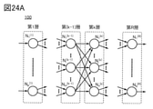
- a calculation is performed by multiplying the synaptic connection strength (sometimes called a weighting factor) that connects two neurons with the signal transmitted between the two neurons.
- the connection strength of each synapse between the plurality of first neurons in the first layer and one of the second neurons in the second layer, and the plurality of first neurons in the first layer. It is necessary to multiply and add each signal input to one of the second neurons of the second layer from, that is, to perform a product-sum calculation of the connection strength and the signal.
- the number of the coupling strengths and the number of parameters indicating the signals used in the product-sum calculation are determined according to the scale of the artificial neural network.
- the second neuron performs an operation by the activation function using the result of the product-sum calculation of the synaptic connection strength and the signal output by the first neuron, and uses the calculation result as a signal in the third layer.
- the circuit constituting the chip has circuit elements that are not easily affected by temperature. Moreover, if the characteristics of the transistor, current source, etc. contained in the chip vary, the calculation result also varies.
- the multiplication cell is provided with a storage element such as a capacity for holding the weighting coefficient, but the data held in the storage element may deteriorate with the passage of time and the value of the weighting coefficient may change. Data degradation is caused by a decrease in the charge held in the storage element.
- the cause of the decrease in electric charge is, for example, the leak current flowing from the storage element, and the types of the leak current are, for example, the leak current flowing in the off state in a switching element such as a transistor, and between a pair of electrodes in a capacitive element.
- the leak current flowing in the off state in a switching element such as a transistor, and between a pair of electrodes in a capacitive element.
- the influence of the leak current can be reduced by increasing the capacitance value of the capacitive element.
- the arithmetic circuit including the multiplication cell needs measures other than increasing the capacitance value of the capacitance element.
- the countermeasure it is possible to periodically rewrite the weighting coefficient to the storage element of the multiplication cell.
- the rewriting of data means the operation of rewriting the same data as the data originally held in the cell.
- rewriting data is also an operation of replenishing the cell whose absolute value of the retained charge amount has become smaller with the same amount of charge originally retained in order to restore the data. It shall point.
- One aspect of the present invention is to provide a semiconductor device or the like that performs product-sum calculation and / or function calculation.
- one aspect of the present invention is to provide a semiconductor device for rewriting the data held in the multiplication cell.
- one aspect of the present invention is to provide a semiconductor device that holds a digital value, performs digital-to-analog conversion on the digital value, and performs an operation based on the analog value.
- one aspect of the present invention is to provide a semiconductor device or the like that performs convolution processing such as CNN (Convolutional Neural Network).
- one aspect of the present invention is to provide a semiconductor device for AI (Artificial Integrity) or the like.
- one aspect of the present invention is to provide a semiconductor device or the like for a DNN (Deep Neural Network).
- DNN Deep Neural Network
- one aspect of the present invention is to provide a semiconductor device or the like having low power consumption.
- one aspect of the present invention is to provide a semiconductor device or the like that is not easily affected by the temperature of the environment.
- one aspect of the present invention is to provide a semiconductor device or the like that is not easily affected by variations in transistor characteristics.
- one aspect of the present invention is to provide a semiconductor device or the like that is not easily affected by variations in the characteristics of a current source.
- one aspect of the present invention is to provide a new semiconductor device or the like.
- the problem of one aspect of the present invention is not limited to the problems listed above.
- the issues listed above do not preclude the existence of other issues.
- Other issues are issues not mentioned in this item, which are described below. Issues not mentioned in this item can be derived from the description of the description, drawings, etc. by those skilled in the art, and can be appropriately extracted from these descriptions.
- one aspect of the present invention solves at least one of the above-listed problems and other problems. It should be noted that one aspect of the present invention does not need to solve all of the above-listed problems and other problems.
- One aspect of the present invention is a semiconductor device including a first circuit, a second circuit, and a third circuit.
- the first circuit has a current source and a first switch
- the second circuit has a first transistor, a third transistor, a fourth transistor, and a first capacitance, and a third circuit.
- the first terminal of the first transistor is electrically connected to the control terminal of the first switch
- the second terminal of the first transistor is electrically connected to the first terminal of the fourth transistor
- the second terminal of the fourth transistor is connected.
- the 2 terminals are electrically connected to the 1st terminal of the 1st capacitance, and the gate of the 4th transistor is electrically connected to the 2nd terminal of the 1st capacitance and the 1st terminal of the 3rd transistor.
- the first terminal of the switch is electrically connected to the output terminal of the current source, and the second terminal of the first switch is electrically connected to the first terminal of the second transistor.
- one aspect of the present invention may be configured to have a fourth circuit including a latch circuit in the above (1). Further, in the electrical connection between the first terminal of the first transistor and the control terminal of the first switch, the first terminal of the fourth circuit is electrically connected to the first terminal of the first transistor, and the first terminal of the fourth circuit is electrically connected. It is assumed that the second terminal is electrically connected to the control terminal of the first switch.
- one aspect of the present invention is a semiconductor device including a first circuit, a second circuit, a third circuit, and a sense amplifier.
- the first circuit has a current source and a first switch
- the second circuit has a first transistor and a first capacitance
- the third circuit has a second transistor.
- the first terminal of the first transistor is electrically connected to the control terminal of the first switch via a sense amplifier
- the second terminal of the first transistor is electrically connected to the first terminal of the first capacitance.
- the first terminal of the first switch is electrically connected to the output terminal of the current source
- the second terminal of the first switch is electrically connected to the first terminal of the second transistor.
- one aspect of the present invention may be a configuration in which the gate of the first transistor is electrically connected to the gate of the second transistor in any one of the above (1) to (3).
- one aspect of the present invention is a semiconductor device having a first circuit, a second circuit, and a third circuit.
- the first circuit has a current source and a first switch
- the second circuit has a first transistor, a third transistor, and a first capacitance
- the third circuit has a second transistor.
- the first terminal of the first transistor is electrically connected to the control terminal of the first switch
- the first terminal of the third transistor is electrically connected to the first terminal of the first capacitance and the gate of the first transistor.
- the first terminal of the first switch is electrically connected to the output terminal of the current source
- the second terminal of the first switch is electrically connected to the first terminal of the second transistor.
- one aspect of the present invention may be configured to include a fourth circuit including a latch circuit. Further, in the electrical connection between the first terminal of the first transistor and the control terminal of the first switch, the first terminal of the fourth circuit is electrically connected to the first terminal of the first transistor, and the first terminal of the fourth circuit is electrically connected. It is assumed that the second terminal is electrically connected to the control terminal of the first switch.
- one aspect of the present invention may be configured in the above (5) or (6) in which the second terminal of the first capacitance is electrically connected to the gate of the second transistor.
- the transistor included in the second circuit may have a metal oxide in the channel forming region.
- one aspect of the present invention is a semiconductor device having a first circuit and a fifth circuit.
- the first circuit has a first current source, a second current source, a first switch, a fifth transistor, and a sixth transistor
- the fifth circuit has a seventh transistor and an eighth transistor.
- the output terminal of the first current source is electrically connected to the first terminal of the first switch
- the output terminal of the second current source is the gate of the fifth transistor, the gate of the sixth transistor, and the sixth transistor. It is preferably electrically connected to the first terminal.
- the first terminal of the seventh transistor is electrically connected to the first terminal of the eighth transistor, the first terminal of the second switch, and the first terminal of the third switch, and is the gate of the seventh transistor. Is preferably electrically connected to the second terminal of the eighth transistor and the first terminal of the second capacitance.
- the second terminal of the first switch is electrically connected to the second terminal of the second switch, and the first terminal of the current comparison circuit is electrically connected to the second terminal of the third switch for current comparison.
- the second terminal of the circuit is preferably electrically connected to the first terminal of the fifth transistor.
- one aspect of the present invention is a semiconductor device having a first circuit and a fifth circuit, which is different from the above (9).
- the first circuit has a first current source, a third current source, a first switch, and a fourth switch
- the fifth circuit has a seventh transistor, an eighth transistor, and a second capacitance.
- a second switch, a third switch, a fifth switch, and a current comparison circuit It is preferable that the output terminal of the first current source is electrically connected to the first terminal of the first switch, and the input terminal of the third current source is electrically connected to the first terminal of the fourth switch. ..
- the first terminal of the seventh transistor is electrically connected to the first terminal of the eighth transistor, the first terminal of the second switch, and the first terminal of the third switch, and is the gate of the seventh transistor. Is preferably electrically connected to the second terminal of the eighth transistor and the first terminal of the second capacitance. It is preferable that the second terminal of the first switch is electrically connected to the second terminal of the second switch, and the second terminal of the fourth switch is electrically connected to the first terminal of the fifth switch. .. It is preferable that the first terminal of the current comparison circuit is electrically connected to the second terminal of the third switch, and the second terminal of the current comparison circuit is electrically connected to the second terminal of the fifth switch. ..
- the seventh transistor has silicon in the channel forming region, and the eighth transistor has a metal oxide in the channel forming region. May be good.
- the fifth circuit may have a configuration including a ninth transistor, a tenth transistor, a third capacitance, and a sixth switch.
- the first terminal of the ninth transistor is electrically connected to the first terminal of the tenth transistor, the first terminal of the second switch, and the first terminal of the sixth switch, and the gate of the ninth transistor is It is preferable that the second terminal of the tenth transistor and the first terminal of the third capacitance are electrically connected to each other. Further, it is preferable that the second terminal of the sixth switch is electrically connected to the first terminal of the fifth switch and the second terminal of the fourth switch. It is preferable that the gate of the 8th transistor and the gate of the 10th transistor are not directly connected.
- each of the 7th transistor and the 9th transistor has silicon in the channel forming region
- each of the 8th transistor and the 10th transistor has silicon in the channel forming region. It may be configured to have a metal oxide.
- one aspect of the present invention is an electronic device having the semiconductor device according to any one of (1) to (13) above and a housing.
- the semiconductor device is a device that utilizes semiconductor characteristics, and refers to a circuit including a semiconductor element (transistor, diode, photodiode, etc.), a device having the same circuit, and the like. It also refers to all devices that can function by utilizing semiconductor characteristics.
- a semiconductor element transistor, diode, photodiode, etc.
- the storage device, the display device, the light emitting device, the lighting device, the electronic device, and the like may be a semiconductor device itself, and may have a semiconductor device.
- an element for example, a switch, a transistor, a capacitive element, an inductor, a resistance element, a diode, a display
- One or more devices, light emitting devices, loads, etc. can be connected between X and Y.
- the switch has a function of controlling on / off. That is, the switch is in a conducting state (on state) or a non-conducting state (off state), and has a function of controlling whether or not a current flows.
- a circuit that enables functional connection between X and Y for example, a logic circuit (inverter, NAND circuit, NOR circuit, etc.), signal conversion) Circuits (digital-analog conversion circuit, analog-to-digital conversion circuit, gamma correction circuit, etc.), potential level conversion circuit (power supply circuit (boost circuit, step-down circuit, etc.), level shifter circuit that changes the potential level of the signal, etc.), voltage source, current source , Switching circuit, amplifier circuit (circuit that can increase signal amplitude or current amount, operational amplifier, differential amplifier circuit, source follower circuit, buffer circuit, etc.), signal generation circuit, storage circuit, control circuit, etc.) It is possible to connect one or more to and from. As an example, even if another circuit is sandwiched between X and Y, if the signal output from X is transmitted to Y, it is assumed that X and Y are functionally connected. do.
- X and Y are electrically connected, it means that X and Y are electrically connected (that is, another element between X and Y). Or when they are connected by sandwiching another circuit) and when X and Y are directly connected (that is, they are connected without sandwiching another element or another circuit between X and Y). If there is) and.
- X and Y, the source (or the first terminal, etc.) and the drain (or the second terminal, etc.) of the transistor are electrically connected to each other, and the X, the source (or the second terminal, etc.) of the transistor are connected to each other. (1 terminal, etc.), the drain of the transistor (or the 2nd terminal, etc.), and Y are electrically connected in this order.
- the source of the transistor (or the first terminal, etc.) is electrically connected to X
- the drain of the transistor (or the second terminal, etc.) is electrically connected to Y
- the first terminal, etc.), the drain of the transistor (or the second terminal, etc.), and Y are electrically connected in this order.
- X is electrically connected to Y via the source (or first terminal, etc.) and drain (or second terminal, etc.) of the transistor, and X, the source (or first terminal, etc.) of the transistor.
- the terminals, etc.), the drain of the transistor (or the second terminal, etc.), and Y are provided in this connection order.
- the source (or first terminal, etc.) and drain (or second terminal, etc.) of the transistor can be separated. Separately, the technical scope can be determined. It should be noted that these expression methods are examples, and are not limited to these expression methods.
- X and Y are objects (for example, devices, elements, circuits, wirings, electrodes, terminals, conductive films, layers, etc.).
- the circuit diagram shows that the independent components are electrically connected to each other, the case where one component has the functions of a plurality of components together.
- one conductive film has both the function of the wiring and the function of the component of the function of the electrode. Therefore, the electrical connection in the present specification also includes the case where one conductive film has the functions of a plurality of components in combination.
- the “resistance element” may be, for example, a circuit element having a resistance value higher than 0 ⁇ , wiring higher than 0 ⁇ , or the like. Therefore, in the present specification and the like, the “resistance element” includes wiring having a resistance value, a transistor in which a current flows between a source and a drain, a diode, a coil, and the like. Therefore, the term “resistance element” may be paraphrased into terms such as “resistance”, “load”, and “region having a resistance value”. On the contrary, the terms “resistance”, “load”, and “region having a resistance value” may be paraphrased into terms such as “resistance element”.
- the resistance value can be, for example, preferably 1 m ⁇ or more and 10 ⁇ or less, more preferably 5 m ⁇ or more and 5 ⁇ or less, and further preferably 10 m ⁇ or more and 1 ⁇ or less. Further, for example, it may be 1 ⁇ or more and 1 ⁇ 10 9 ⁇ or less.
- the “capacitance element” means, for example, a circuit element having a capacitance value higher than 0F, a wiring region having a capacitance value higher than 0F, a parasitic capacitance, and a transistor. It can be the gate capacitance of. Therefore, in the present specification and the like, the “capacitive element” includes a pair of electrodes and a circuit element including a dielectric contained between the electrodes. In addition, terms such as “capacitive element”, “parasitic capacitance”, and “gate capacitance” may be paraphrased into terms such as "capacity”.
- the term “capacity” may be paraphrased into terms such as “capacitive element”, “parasitic capacitance”, and “gate capacitance”.
- the term “pair of electrodes” of “capacity” can be paraphrased as “pair of conductors", “pair of conductive regions", “pair of regions” and the like.
- the value of the capacitance can be, for example, 0.05 fF or more and 10 pF or less. Further, for example, it may be 1 pF or more and 10 ⁇ F or less.
- the transistor has three terminals called a gate, a source, and a drain.
- the gate is a control terminal that controls the conduction state of the transistor.
- the two terminals that function as sources or drains are the input and output terminals of the transistor.
- One of the two input / output terminals becomes a source and the other becomes a drain depending on the high and low potentials given to the conductive type (n-channel type and p-channel type) of the transistor and the three terminals of the transistor. Therefore, in the present specification and the like, the terms source and drain may be paraphrased with each other.
- the transistor when explaining the connection relationship of transistors, "one of the source or drain” (or the first electrode or the first terminal), “the other of the source or drain” (or the second electrode, or the second electrode, or The notation (second terminal) is used.
- it may have a back gate in addition to the above-mentioned three terminals.
- one of the gate or the back gate of the transistor may be referred to as a first gate
- the other of the gate or the back gate of the transistor may be referred to as a second gate.
- the terms “gate” and “backgate” may be interchangeable.
- the respective gates When the transistor has three or more gates, the respective gates may be referred to as a first gate, a second gate, a third gate, and the like in the present specification and the like.
- a transistor having a multi-gate structure having two or more gate electrodes can be used as an example of a transistor.
- the multi-gate structure since the channel formation regions are connected in series, a structure in which a plurality of transistors are connected in series is obtained. Therefore, the multi-gate structure can reduce the off-current and improve the withstand voltage of the transistor (improve the reliability).
- the multi-gate structure even if the voltage between the drain and the source changes when operating in the saturation region, the current between the drain and the source does not change much, and the slope is flat. The characteristics can be obtained. By utilizing the voltage / current characteristics with a flat slope, it is possible to realize an ideal current source circuit or an active load having a very high resistance value. As a result, it is possible to realize a differential circuit or a current mirror circuit having good characteristics.
- the circuit element may have a plurality of circuit elements.
- one resistance is described on the circuit diagram, it includes the case where two or more resistances are electrically connected in series.
- one capacity is described on the circuit diagram, it includes a case where two or more capacities are electrically connected in parallel.
- one transistor is described on the circuit diagram, two or more transistors are electrically connected in series, and the gates of the respective transistors are electrically connected to each other.
- Shall include.
- the switch has two or more transistors, and two or more transistors are electrically connected in series or in parallel. It is assumed that the gates of the respective transistors are electrically connected to each other.
- a node can be paraphrased as a terminal, a wiring, an electrode, a conductive layer, a conductor, an impurity region, etc., depending on a circuit configuration, a device structure, and the like.
- terminals, wiring, etc. can be paraphrased as nodes.
- ground potential ground potential
- the potentials are relative, and when the reference potential changes, the potential given to the wiring, the potential applied to the circuit, the potential output from the circuit, and the like also change.
- the terms “high level potential” and “low level potential” do not mean a specific potential.
- the high level potentials provided by both wirings do not have to be equal to each other.
- the low-level potentials provided by both wirings do not have to be equal to each other. ..
- the "current” is a charge transfer phenomenon (electrical conduction).
- the description “electrical conduction of a positively charged body is occurring” means “electrical conduction of a negatively charged body in the opposite direction”. Is happening. " Therefore, in the present specification and the like, “current” refers to a charge transfer phenomenon (electrical conduction) associated with carrier transfer, unless otherwise specified.
- the carrier here include electrons, holes, anions, cations, complex ions, and the like, and the carriers differ depending on the system in which the current flows (for example, semiconductor, metal, electrolyte, in vacuum, etc.).
- the "current direction” in wiring or the like is the direction in which the carrier that becomes a positive charge moves, and is described as a positive current amount.
- the direction in which the carrier that becomes a negative charge moves is opposite to the direction of the current, and is expressed by the amount of negative current. Therefore, in the present specification and the like, if there is no disclaimer regarding the positive or negative current (or the direction of the current), the description such as “current flows from element A to element B” means “current flows from element B to element A”. Can be rephrased as. Further, the description such as “a current is input to the element A” can be rephrased as "a current is output from the element A” or the like.
- the ordinal numbers “1st”, “2nd”, and “3rd” are added to avoid confusion of the components. Therefore, the number of components is not limited. Moreover, the order of the components is not limited. For example, the component referred to in “first” in one of the embodiments of the present specification and the like may be the other embodiment or the component referred to in “second” in the scope of claims. There can also be. Further, for example, the component referred to in “first” in one of the embodiments of the present specification and the like may be omitted in other embodiments or in the scope of claims.
- the terms “upper” and “lower” do not limit the positional relationship of the components to be directly above or directly below and to be in direct contact with each other.
- the terms “electrode B on the insulating layer A” it is not necessary that the electrode B is formed in direct contact with the insulating layer A, and another configuration is formed between the insulating layer A and the electrode B. Do not exclude those that contain elements.
- words such as “membrane” and “layer” can be interchanged with each other depending on the situation.
- the terms “insulating layer” and “insulating film” may be changed to the term "insulator”.
- Electrode may be used as part of a “wiring” and vice versa.
- terms such as “electrode” and “wiring” include the case where a plurality of “electrodes”, “wiring” and the like are integrally formed.
- a “terminal” may be used as part of a “wiring”, “electrode”, etc., and vice versa.
- the term “terminal” includes a case where a plurality of "electrodes", “wiring”, “terminals” and the like are integrally formed.
- the "electrode” can be a part of “wiring” or “terminal”, and for example, “terminal” can be a part of “wiring” or “electrode”. Further, terms such as “electrode”, “wiring”, and “terminal” may be replaced with terms such as "area” in some cases.
- terms such as “wiring”, “signal line”, and “power line” can be interchanged with each other in some cases or depending on the situation.
- the reverse is also true, and it may be possible to change terms such as “signal line” and “power line” to the term “wiring”.
- a term such as “power line” may be changed to a term such as "signal line”.
- a term such as “signal line” may be changed to a term such as “power line”.
- the term “potential” applied to the wiring may be changed to a term such as “signal” in some cases or depending on the situation.
- the reverse is also true, and terms such as “signal” may be changed to the term “potential”.
- the semiconductor impurities refer to, for example, other than the main components constituting the semiconductor layer.
- an element having a concentration of less than 0.1 atomic% is an impurity.
- the inclusion of impurities may result in, for example, an increase in the defect level density of the semiconductor, a decrease in carrier mobility, a decrease in crystallinity, and the like.
- the impurities that change the characteristics of the semiconductor include, for example, group 1 element, group 2 element, group 13 element, group 14 element, group 15 element, and other than the main component.
- the impurities that change the characteristics of the semiconductor include, for example, Group 1 elements, Group 2 elements, Group 13 elements, Group 15 elements and the like (however, oxygen, Does not contain hydrogen).
- the switch means a switch that is in a conductive state (on state) or a non-conducting state (off state) and has a function of controlling whether or not a current flows.
- the switch means a switch having a function of selecting and switching a path through which a current flows. Therefore, the switch may have two or three or more terminals through which a current flows, in addition to the control terminals.
- an electric switch, a mechanical switch, or the like can be used. That is, the switch is not limited to a specific switch as long as it can control the current.
- Examples of electrical switches include transistors (for example, bipolar transistors, MOS transistors, etc.), diodes (for example, PN diodes, PIN diodes, shotkey diodes, MIM (Metal Insulator Metal) diodes, and MIS (Metal Insulator Semiconductor) diodes. , Diode-connected transistors, etc.), or logic circuits that combine these.
- transistors for example, bipolar transistors, MOS transistors, etc.
- diodes for example, PN diodes, PIN diodes, shotkey diodes, MIM (Metal Insulator Metal) diodes, and MIS (Metal Insulator Semiconductor) diodes. , Diode-connected transistors, etc.
- the "conduction state" of the transistor is, for example, a state in which the source electrode and the drain electrode of the transistor can be regarded as being electrically short-circuited, and a current is applied between the source electrode and the drain electrode. It means a state where it
- the "non-conducting state" of the transistor means a state in which the source electrode and the drain electrode of the transistor can be regarded as being electrically cut off.
- the polarity (conductive type) of the transistor is not particularly limited.
- An example of a mechanical switch is a switch that uses MEMS (Micro Electro Mechanical Systems) technology.
- the switch has an electrode that can be moved mechanically, and by moving the electrode, conduction and non-conduction are controlled and operated.
- parallel means a state in which two straight lines are arranged at an angle of -10 ° or more and 10 ° or less. Therefore, the case of ⁇ 5 ° or more and 5 ° or less is also included.
- substantially parallel or approximately parallel means a state in which two straight lines are arranged at an angle of -30 ° or more and 30 ° or less.
- vertical means a state in which two straight lines are arranged at an angle of 80 ° or more and 100 ° or less. Therefore, the case of 85 ° or more and 95 ° or less is also included.
- substantially vertical or “approximately vertical” means a state in which two straight lines are arranged at an angle of 60 ° or more and 120 ° or less.
- a semiconductor device or the like that performs a product-sum calculation and / or a function calculation.
- a semiconductor device for rewriting the data held in the multiplication cell can provide a semiconductor device that holds a digital value, performs digital-to-analog conversion on the digital value, and performs an operation based on the analog value.
- a semiconductor device or the like that performs a convolution process such as CNN.
- a semiconductor device or the like for AI can be provided.
- a semiconductor device or the like for DNN can be provided.
- a semiconductor device or the like having low power consumption it is possible to provide a semiconductor device or the like that is not easily affected by the temperature of the environment.
- a semiconductor device or the like that is not easily affected by variations in the characteristics of the transistor it is possible to provide a semiconductor device or the like that is not easily affected by variations in the characteristics of the current source.
- a novel semiconductor device or the like can be provided.
- the effect of one aspect of the present invention is not limited to the effects listed above.
- the effects listed above do not preclude the existence of other effects.
- the other effects are the effects not mentioned in this item, which are described below. Effects not mentioned in this item can be derived from the description in the specification, drawings, etc. by those skilled in the art, and can be appropriately extracted from these descriptions.
- one aspect of the present invention has at least one of the above-listed effects and other effects. Therefore, one aspect of the present invention may not have the effects listed above in some cases.
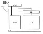
- FIG. 1A and 1B are block diagrams showing a configuration example of a semiconductor device
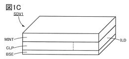
- FIG. 1C is a perspective view showing a configuration example of the semiconductor device
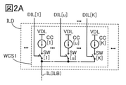
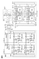
- 2A to 2C are circuits showing a configuration example of a circuit included in the semiconductor device.
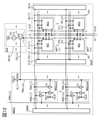
- FIG. 3 is a circuit diagram showing a configuration example of a circuit included in a semiconductor device.
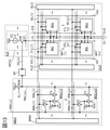
- FIG. 4 is a circuit diagram showing a configuration example of a circuit included in a semiconductor device.
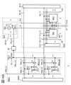
- FIG. 5 is a circuit diagram showing a configuration example of a circuit included in a semiconductor device.
- FIG. 6 is a circuit diagram showing a configuration example of a circuit included in a semiconductor device.
- 7A to 7E are circuit diagrams showing a configuration example of a circuit included in the semiconductor device.
- FIG. 1A and 1B are block diagrams showing a configuration example of a semiconductor device
- FIG. 1C is a perspective view showing a configuration example of the semiconductor device.
- FIG. 3 is a circuit diagram showing a configuration
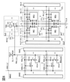
- FIG. 8 is a circuit diagram showing a configuration example of a circuit included in the semiconductor device.
- FIG. 9 is a circuit diagram showing a configuration example of a circuit included in the semiconductor device.
- 10A is a circuit diagram showing a configuration example of a circuit included in the semiconductor device, and
- FIGS. 10B to 10E are circuit diagrams showing a configuration example of a memory cell included in the semiconductor device.
- FIG. 11 is a circuit diagram showing a configuration example of a circuit included in the semiconductor device.
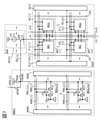
- FIG. 12 is a circuit diagram showing a configuration example of a circuit included in the semiconductor device.
- FIG. 13 is a circuit diagram showing a configuration example of a circuit included in the semiconductor device.
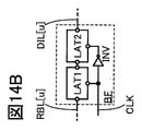
- FIG. 14A is a circuit diagram showing a configuration example of a circuit included in the semiconductor device, and FIG.
- FIG. 14B is a circuit diagram showing a configuration example of a part of the circuit included in the circuit.
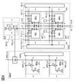
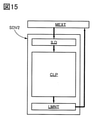
- FIG. 15 is a block diagram showing a configuration example of a semiconductor device.
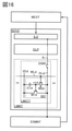
- FIG. 16 is a block diagram showing a configuration example of a semiconductor device.
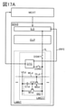
- FIG. 17A is a block diagram showing a configuration example of a semiconductor device, and
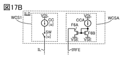
- FIG. 17B is a circuit diagram showing a configuration example of a circuit included in the semiconductor device.
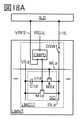
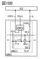
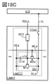
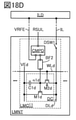
- 18A to 18D are circuit diagrams showing a configuration example of a semiconductor device.
- FIG. 19 is a circuit diagram showing a configuration example of a circuit included in a semiconductor device.
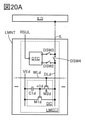
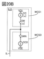
- FIG. 20A is a circuit diagram showing a configuration example of a semiconductor device, and FIG.
- 20B is a circuit diagram showing a configuration example of a circuit included in the semiconductor device.
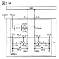
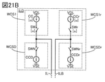
- 21A is a circuit diagram showing a configuration example of a semiconductor device
- FIG. 21B is a circuit diagram showing a configuration example of a circuit included in the semiconductor device.
- 22A and 22B are circuit diagrams showing a configuration example of a semiconductor device.
- FIG. 23 is a block diagram showing a configuration example of the semiconductor device.
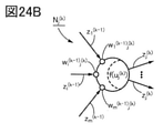
- 24A and 24B are diagrams illustrating a hierarchical neural network.
- FIG. 25 is a circuit diagram showing a configuration example of a circuit included in the semiconductor device.
- FIG. 26 is a circuit diagram showing a configuration example of a circuit included in a semiconductor device.
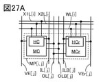
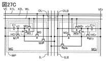
- 27A to 27C are circuit diagrams showing a configuration example of a circuit included in the semiconductor device.
- FIG. 28 is a circuit diagram showing a configuration example of a circuit included in the semiconductor device.
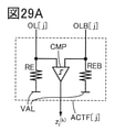
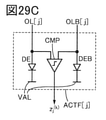
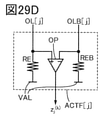
- 29A to 29F are circuit diagrams showing a configuration example of a circuit included in the semiconductor device.
- FIG. 30 is a circuit diagram showing a configuration example of a circuit included in a semiconductor device.
- FIG. 31 is a circuit diagram showing a configuration example of a circuit included in the semiconductor device.
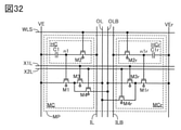
- FIG. 32 is a circuit diagram showing a configuration example of a circuit included in the semiconductor device.
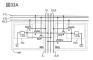
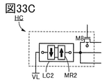
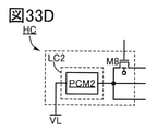
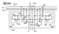
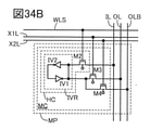
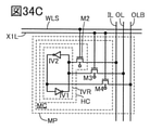
- 33A to 33E are circuit diagrams showing a configuration example of a circuit included in the semiconductor device.
- 34A to 34C are circuit diagrams showing a configuration example of a circuit included in the semiconductor device.
- FIG. 35 is a schematic cross-sectional view showing a configuration example of a semiconductor device.
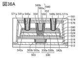
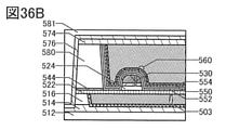
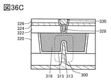
- FIG. 36A to 36C are schematic cross-sectional views showing a configuration example of a transistor.
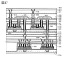
- FIG. 37 is a schematic cross-sectional view showing a configuration example of a semiconductor device.
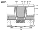
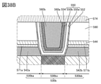
- 38A and 38B are schematic cross-sectional views showing a configuration example of a transistor.
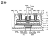
- FIG. 39 is a schematic cross-sectional view showing a configuration example of the transistor.
- FIG. 40A is a diagram for explaining the classification of the crystal structure of IGZO
- FIG. 40B is a diagram for explaining the XRD spectrum of crystalline IGZO
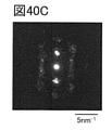
- FIG. 40C is a diagram for explaining the microelectron diffraction pattern of crystalline IGZO.
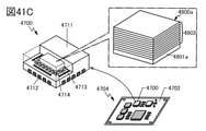
- .. 41A is a perspective view showing an example of a semiconductor wafer
- FIG. 41A is a perspective view showing an example of a semiconductor wafer
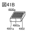
- FIG. 41B is a perspective view showing an example of a chip
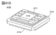
- FIGS. 41C and 41D are perspective views showing an example of an electronic component.
- FIG. 42 is a schematic view showing an example of an electronic device.
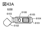
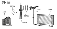
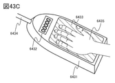
- 43A to 43C are schematic views showing an example of an electronic device.
- the synaptic connection strength can be changed by giving existing information to the neural network.
- the process of giving existing information to the neural network and determining the bond strength may be called "learning”.
- neural network models include Hopfield type and hierarchical type.
- a neural network having a multi-layer structure may be referred to as a “deep neural network” (DNN), and machine learning by a deep neural network may be referred to as “deep learning”.
- DNN deep neural network
- machine learning by a deep neural network may be referred to as “deep learning”.
- a metal oxide is a metal oxide in a broad sense. Metal oxides are classified into oxide insulators, oxide conductors (including transparent oxide conductors), oxide semiconductors (also referred to as Oxide Semiconductor or simply OS) and the like. For example, when a metal oxide is contained in the channel forming region of a transistor, the metal oxide may be referred to as an oxide semiconductor. That is, when a metal oxide can form a channel forming region of a transistor having at least one of an amplification action, a rectifying action, and a switching action, the metal oxide is referred to as a metal oxide semiconductor. be able to. Further, when the term "OS transistor" is used, it can be rephrased as a transistor having a metal oxide or an oxide semiconductor.
- a metal oxide having nitrogen may also be collectively referred to as a metal oxide. Further, the metal oxide having nitrogen may be referred to as a metal oxynitride.
- the configuration shown in each embodiment can be appropriately combined with the configuration shown in other embodiments to form one aspect of the present invention. Further, when a plurality of configuration examples are shown in one embodiment, the configuration examples can be appropriately combined with each other.
- the content described in one embodiment (may be a part of the content) is different from the content described in the embodiment (may be a part of the content) and one or more different implementations. It is possible to apply, combine, or replace at least one content with the content described in the form of (may be a part of the content).
- figure (which may be a part) described in one embodiment is different from another part of the figure, another figure (which may be a part) described in the embodiment, and one or more different figures.
- the figure (which may be a part) described in the embodiment is different from another part of the figure, another figure (which may be a part) described in the embodiment, and one or more different figures.
- more figures can be formed.
- the code is used for identification such as "_1", “[n]”, “[m, n]”. May be added and described. Further, in the drawings and the like, when the reference numerals such as “_1”, “[n]” and “[m, n]” are added to the reference numerals, when it is not necessary to distinguish them in the present specification and the like, when it is not necessary to distinguish them.
- the identification code may not be described.
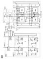
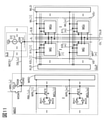
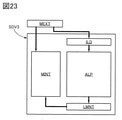
- FIG. 1A is a block diagram showing a configuration example of the semiconductor device SDV1 which is one aspect of the present invention.
- the semiconductor device SDV1 has, for example, a storage device MINT, a circuit ILD, and a calculation unit CLP. Further, FIG. 1A also shows a storage device TEXT in order to show the configuration of an electrical connection with the semiconductor device SDV1.
- the storage device MEM is provided outside the semiconductor device SDV1 as an example.
- the storage device MEM holds data for performing an operation in the arithmetic unit CLP.
- the storage device MEXT transmits the data to the storage device MINT as a digital voltage signal or the like.
- the storage device MEXT may transmit the data not only to the storage device MINT but also to the circuit ILD described later. That is, the semiconductor device SDV1 may be configured so that the storage device MINT and the circuit ILD can be switched as the transmission destination of the storage device MEM.
- the semiconductor device SDV1 when the semiconductor device SDV1 is configured so that the storage device MINT and the circuit ILD can be switched as the transmission destination of the signal output from the storage device MEXT, when data is transmitted from the storage device MEXT to the storage device MINT, it is stored. In order to reduce the memory capacity of the device MINT, the number of bits of the data may be reduced. Further, when data is transmitted from the storage device MEM to the circuit ILD, the number of bits of the data may be increased. Alternatively, when data is transmitted from the storage device MEXT to the storage device MINT, a high bit value of the data is transmitted in order to reduce the memory capacity of the storage device MINT, and a low bit value is required. A low bit value may be input from the storage device TEXT to the circuit ILD. That is, the storage device MINT and the storage device MEM may be input to the circuit ILD at the same time.
- the storage device MEM can be, for example, a storage such as an HDD (hard disk drive) or SSD (solid state drive).
- HDD hard disk drive
- SSD solid state drive
- the semiconductor device SDV1 can be manufactured, for example, by forming a circuit element or the like on one substrate BSE.
- various substrates can be used.
- various substrates include semiconductor substrates (for example, single crystal substrate or silicon substrate), SOI substrates, glass substrates, quartz substrates, plastic substrates, sapphire glass substrates, metal substrates, stainless steel substrates, and stainless still foils.
- glass substrates include barium borosilicate glass, aluminoborosilicate glass, and soda lime glass.
- Examples of flexible substrates, laminated films, base films, etc. include the following.
- plastics typified by polyethylene terephthalate (PET), polyethylene naphthalate (PEN), polyether sulfone (PES), and polytetrafluoroethylene (PTFE).
- PET polyethylene terephthalate
- PEN polyethylene naphthalate
- PES polyether sulfone
- PTFE polytetrafluoroethylene
- a synthetic resin such as acrylic.
- polypropylene polyester, polyvinyl fluoride, polyvinyl chloride and the like.
- polyamide, polyimide, aramid, epoxy resin, inorganic thin-film film, papers and the like are examples of plastics typified by polyethylene terephthalate (PET), polyethylene naphthalate (PEN), polyether sulfone (PES), and polytetrafluoroethylene (PTFE).
- acrylic polypropylene
- polyester polyvinyl fluoride
- polyvinyl chloride polyvinyl chloride
- a transistor using a semiconductor substrate, a single crystal substrate, an SOI substrate, or the like, it is possible to manufacture a transistor having a high current capacity and a small size with little variation in characteristics, size, or shape. ..
- a circuit is configured with such transistors, it is possible to reduce the power consumption of the circuit or increase the integration of the circuit.
- a flexible substrate may be used as the substrate BSE, and a transistor may be formed directly on the flexible substrate.
- a release layer may be provided between the substrate and the transistor. The release layer can be used to separate a part or all of the semiconductor device from the substrate and transfer it to another substrate. At that time, the transistor can be reprinted on a substrate having inferior heat resistance, a flexible substrate, or the like.
- a structure in which an inorganic film of a tungsten film and a silicon oxide film is laminated, a structure in which an organic resin film such as polyimide is formed on a substrate, or the like can be used.
- a transistor may be formed using one substrate, then the transistor may be transposed to another substrate, and the transistor may be arranged on another substrate (for example, substrate BSE).
- substrate BSE a substrate on which the transistor is translocated
- silk, cotton, linen synthetic fibers
- nylon, polyurethane, polyester or recycled fibers (including acetate, cupra, rayon, recycled polyester), leather substrates, rubber substrates, etc.
- a part of the circuit necessary for realizing a predetermined function is formed on one board, and another part of the circuit necessary for realizing a predetermined function is formed on another board. It is possible. For example, a part of the circuit necessary to realize a predetermined function is formed on a glass substrate, and another part of the circuit necessary to realize a predetermined function is a single crystal substrate (or SOI substrate). Can be formed into. Then, a single crystal substrate (also referred to as an IC chip) on which another part of the circuit necessary for realizing a predetermined function is formed is connected to the glass substrate by COG (Chip On Glass) to be connected to the glass substrate.
- COG Chip On Glass
- the IC chip can be placed in the glass.
- the IC chip can be connected to a glass substrate using a TAB (Tape Automated Bonding), COF (Chip On Film), SMT (Surface Mount Technology), a printed circuit board, or the like.
- TAB Transmission Automated Bonding
- COF Chip On Film
- SMT Surface Mount Technology
- a printed circuit board or the like.
- a circuit having a large drive voltage or a circuit having a high drive frequency often consumes a large amount of power. Therefore, such a circuit is formed on a substrate (for example, a single crystal substrate) different from the pixel portion to form an IC chip. By using this IC chip, it is possible to prevent an increase in power consumption.
- each of the transistor included in the arithmetic unit CLP and the transistor included in the circuit ILD can be formed on the substrate BSE as Si transistors. ..
- the transistor included in the storage device MINT as an OS transistor, the storage device MINT can be provided above the arithmetic unit CLP and / or the circuit ILD. That is, as an example, the semiconductor device SDV1 has a configuration in which a calculation unit CLP and a circuit ILD are provided above the substrate BSE, and a storage device MINT is provided above the calculation unit CLP and the circuit ILD, as shown in FIG. 1C. Can be.
- the storage device MINT provided in the semiconductor device SDV1 has a function of acquiring information read by a storage device MEM provided outside the semiconductor device SDV1 and holding the information. Further, the storage device MINT has a function of reading the information held in the storage device MINT and transmitting the information to the circuit ILD.
- the information sent from the storage device MEXT to the storage device MINT is treated as data for performing a calculation by the calculation unit CLP described later.
- the storage device MINT will be described as a configuration for storing digital values.
- the storage device MINT as a storage device that stores as a digital value, even if the absolute value of the amount of charge held in the storage element decreases, the range of potential at which data can be read out is large, so it is the same as when writing. No data can be read.
- the data stored in the storage element can be easily refreshed, so that the potential (charge) held in the storage element can be maintained for a long time. Therefore, it is preferable that the storage device MINT has a function of refreshing the data held periodically.
- the refresh operation may be performed after the data is transmitted to the arithmetic unit CLP (circuit ILD) described later.
- data refresh means that the voltage corresponding to the data of the storage element is read out and the voltage is boosted or stepped down to an appropriate level by an amplifier circuit such as a sense amplifier. , The operation of writing back to the storage element.
- the data may be read from the storage device MEM and written to the memory cell.
- the storage device MINT according to the semiconductor device of the present invention may be configured to store not only digital values but also multi-valued values, analog values and the like.
- the number of bits of the memory cell should be smaller than the number of bits held in the multiplication cell of the arithmetic unit CLP.
- a plurality of memory cells of the storage device MINT can be associated with one multiplication cell of the arithmetic unit CLP. For example, if a 4-bit value can be held in one memory cell of the storage device MINT and an 8-bit value can be held in one multiplication cell of the arithmetic unit CLP, two 4-bit values can be held in the memory cell of the storage device MINT. By writing, an 8-bit value can be written in the multiplication cell of the arithmetic unit CLP.
- examples of the metal oxide contained in the channel forming region of the OS transistor include indium, an In-M-Zn oxide having element M and zinc (element M is aluminum, gallium, ittrium, tin, copper and vanadium). , Berylium, boron, titanium, iron, nickel, germanium, zirconium, molybdenum, lanthanum, cerium, neodymium, hafnium, tantalum, tungsten, magnesium, etc.).
- a transistor having silicon in the channel forming region hereinafter, referred to as a Si transistor may be applied.
- the silicon for example, single crystal silicon, amorphous silicon (sometimes referred to as hydride amorphous silicon), microcrystalline silicon, polycrystalline silicon, or the like can be used.
- the transistor other than the OS transistor and the Si transistor for example, a transistor in which Ge and the like are included in the channel forming region, and a compound semiconductor such as ZnSe, CdS, GaAs, InP, GaN, and SiGe are included in the channel forming region.
- Transistors, transistors in which carbon nanotubes are contained in the channel forming region, transistors in which organic semiconductors are contained in the channel forming region, and the like can be used.
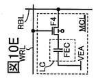
- the circuit ILD functions as a current source circuit for supplying a current to the arithmetic unit CLP as an example. Specifically, the circuit ILD supplies a current corresponding to the information read from the storage device MINT to the circuit included in the arithmetic unit CLP.
- the circuit ILD is not a current source circuit for supplying a current to the arithmetic unit CLP, but a voltage source circuit for inputting a voltage corresponding to the information read from the storage device MINT to the arithmetic unit CLP, for example. (Voltage generation circuit) may be used.
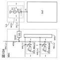
- the arithmetic unit CLP has a plurality of circuits that function as multiplication cells. Further, as an example, the multiplication cell has a function of holding data used for calculation as an analog value. Further, in the arithmetic unit CLP, it is assumed that the circuits are arranged in a matrix. Further, the circuit holds the information (for example, current, voltage, etc.) sent from the circuit ILD, and then inputs the voltage corresponding to the multiplier to the arithmetic unit CLP, so that the value corresponding to the information is obtained. The product of and the multiplier can be calculated.
- the information for example, current, voltage, etc.
- the sum of the currents is obtained by adding the currents output from the plurality of circuits to each other (each information held in the plurality of circuits). For example, it can be an amount corresponding to the value of the sum of products of current, voltage, etc.) and a plurality of multipliers. Further, it is assumed that the arithmetic unit CLP also includes a drive circuit for operating the multiplication cell.
- the circuit configuration of the calculation unit CLP and the principle of the product-sum calculation in the calculation unit CLP will be described in detail in the second embodiment.
- the storage device MINT has a function of holding a digital value and the storage device MINT has a function of holding an analog value in the multiplication cell of the calculation unit CLP
- the storage device MINT transmits the data used for the calculation to the calculation unit, it is digital. It is necessary to perform analog conversion.
- the circuit ILD has not only the function of the current source circuit but also the function of the digital-to-analog conversion circuit. Further, the larger the analog data to be written to the arithmetic unit CLP, the larger the memory capacity required for the storage device MINT.
- the storage device MINT requires eight binary memory cells.
- the semiconductor device SDV1 is stored above the arithmetic unit CLP (including the circuit for driving the arithmetic unit CLP) and the circuit ILD as shown in FIG. 1C described above. It is preferable to have a configuration provided with the device MINT. Further, by applying the trench type as the capacity that can be provided in the memory cell of the storage device MINT, the area of each memory cell can be reduced.
- the semiconductor device SDV1 periodically converts the digital data (the same value as the data held in the multiplication cell) held in the storage device MINT from the storage device MINT into analog data by the circuit ILD. It is preferable to transmit the analog data to the calculation unit CLP and write it again to the storage element of the multiplication cell of the calculation unit CLP (input current, voltage, etc., or replenish the charge).
- the storage device MINT functions as a circuit for holding digital data corresponding to the analog data in order to compensate for the analog data held in the storage element of the multiplication cell of the arithmetic unit CLP.
- the storage device MINT may be referred to as a main memory for the arithmetic unit CLP.
- the storage element provided in the multiplication cell of the arithmetic unit CLP can be considered as a temporary memory.
- the memory cell MCL of the storage device MINT is a circuit capable of holding digital data (2 bits) and the multiplication cell of the arithmetic unit CLP is a circuit capable of holding analog data corresponding to 8 bits.
- the storage device MINT Since the memory cell MCL of the storage device MINT can hold data longer than the multiplication cell of the arithmetic unit CLP (because the data value is unlikely to change due to a decrease in the absolute value of the amount of charge due to the leak current), the storage device It is preferable to treat the MINT as the main memory. Further, since the calculation for handling analog data has higher calculation efficiency than the calculation for handling digital data, the semiconductor device SDV1 converts the digital data read from the storage device MINT into analog data, and the calculation unit CLP converts the analog data. It is preferable that the configuration is such that the operations to be handled are performed.
- the semiconductor device SDV1 may have a plurality of arithmetic units CLP.
- the arithmetic unit CLPa and the arithmetic unit CLPb may be provided instead of the arithmetic unit CLP of FIG. 1A.
- the semiconductor device SDV1 writes data transmitted from the storage device MINT to, for example, either the arithmetic unit CLPa or the arithmetic unit CLPb, and the arithmetic unit CLPa in the meantime.
- the calculation can be performed on the other side of the calculation unit CLPb.
- one of the calculation unit CLPa or the calculation unit CLPb may be a circuit for performing analog calculation
- the other of the calculation unit CLPa or the calculation unit CLPb may be a circuit for performing digital calculation
- both the calculation unit CLPa and the calculation unit CLPb may be used as a circuit for performing digital calculation.
- Circuit ILD a VI conversion circuit (sometimes called a digital-to-analog conversion circuit) that outputs an analog current based on a digital value read from the storage device MINT will be described as a circuit ILD.
- the circuit ILD shown in FIG. 2A is an example of a current source circuit applicable to the circuit ILD of FIG. 1A.
- the circuit ILD of FIG. 2A has a circuit WCS1, and the circuit WCS1 includes a constant current source CC [1] to a constant current source CC [K] (K is an integer of 1 or more) and switches SW [1] to. It has a switch SW [K].
- the input terminal of the constant current source CC [u] (u is an integer of 1 or more and K or less) is electrically connected to the wiring VDC, and the output terminal of the constant current source CC [u] is the switch SW [u]. ] Is electrically connected to the first terminal, and the second terminal of the switch SW [u] is electrically connected to the wiring IL. Further, the control terminal of the switch SW [u] is electrically connected to the wiring DIL [u].
- the wiring DIL [1] to the wiring DIL [K] shown in FIG. 2A are electrically connected to the storage device MINT included in the semiconductor device SDV1 of FIG. 1A. That is, the wiring DIL [1] to the wiring DIL [K] functions as wiring for transmitting the information read from the storage device MINT.
- the wiring VLL functions as a wiring that gives a constant voltage as an example.
- the constant voltage is preferably, for example, a high level potential.
- the wiring IL functions as wiring for electrically connecting to the arithmetic unit CLP. That is, the wiring IL functions as wiring for passing the current generated by the circuit ILD according to the information held in the storage device MINT to the arithmetic unit CLP.
- the wiring IL functions as, for example, a row of write data lines extending to the arithmetic unit CLP. Therefore, when the arithmetic unit CLP has a plurality of columns of multiplication cells, it is preferable that the circuit ILD has a plurality of circuits WCS1. Further, depending on the configuration of the calculation unit CLP, two write data lines may be provided in a plurality of multiplication cells arranged in one column. Therefore, in FIG. 2A, one wiring is shown as a wiring IL, and the other wiring is shown as a wiring ILB in parentheses.
- the circuit WCS1 of FIG. 2A has a function of outputting information of K bits (2 K value) (K is an integer of 1 or more) as a current.
- K is an integer of 1 or more
- the information corresponding to the value of the first bit is input to the wiring DIL [1]
- the information corresponding to the value of the u-bit is input to the wiring DIL [u]
- the value of the K-bit is input.
- constant current constant current source CC [u] shed is set to 2 u-1 ⁇ I ut
- a constant current source CC [K] is constant current is preferable to be 2 K-1 ⁇ I ut flow.
- a decoder DEC for converting a binary number to a decimal number may be provided between the storage device MINT and the circuit ILD.
- the circuit configuration of the circuit ILD in this case is shown in FIG. 2B.
- the circuit WCS2 included in the circuit ILD includes a constant current source CC [1] to a constant current source CC [2 K -1] and a switch SW [1] to a switch SW [2 K -1]. ] And.
- the decoder DEC is electrically connected to the wiring DIL [1] to the wiring DIL [K], also it is electrically connected to the wiring DEL [1] to the wiring DEL [2 K -1]. Further, the input terminal of the constant current source CC [t] (t is an integer of 1 or more and 2K -1 or less) is electrically connected to the wiring VDC, and the output terminal of the constant current source CC [t] is. , The second terminal of the switch SW [t] is electrically connected to the first terminal of the switch SW [t], and the second terminal of the switch SW [t] is electrically connected to the wiring IL. Further, the control terminal of the switch SW [t] is electrically connected to the wiring DEL [t].
- the decoder DEC converts the K-bit (binary number) information sent to the wiring DIL [1] to the wiring DIL [K] into decimal information, and converts the wiring DEL [1] to the wiring DEL [2 K -1]. Has a function to send to.
- the circuit WCS2 of FIG. 2B has a function of outputting information of K bits (2 K value) (K is an integer of 1 or more) as a current, similarly to the circuit WCS1 of FIG. 2A.
- K is an integer of 1 or more
- the constant current amount passed by each of the constant current source CC [1] to the constant current source CC [2K -1] is I. It is preferably ut.
- the constant current source CC included in the circuit WCS1 of FIG. 2A and the circuit WCS2 of FIG. 2B may be configured to have a transistor, for example.
- a switch SW included in the circuit WCS1 of FIG. 2A and the circuit WCS2 of FIG. 2B for example, an electric switch such as an analog switch or a transistor can be applied.
- a mechanical switch may be applied.
- the switch SW shall be turned off when a high level potential is applied to the control terminal and turned on when a low level potential is applied to the control terminal.
- the constant current source CC [1] has a transistor CTr [1]
- the constant current source CC [u] has a transistor CTr [u].
- the constant current source CC [K] has a transistor CTr [K]
- the switch SW [1] has a transistor STR [1]
- the switch SW [u] has a transistor STR [u]
- the circuit configuration is such that SW [K] has a transistor Str [K].
- a Si transistor as each of the transistor CTr [1] to the transistor CTr [K] and the transistor STR [1] to the transistor STR [K] shown in FIG. 2C.
- a transistor other than the Si transistor for example, a transistor in which Ge or the like is included in the channel forming region, or a transistor in which a compound semiconductor such as ZnSe, CdS, GaAs, InP, GaN, SiGe or the like is included in the channel forming region.
- Transistors in which carbon nanotubes are contained in the channel forming region, transistors in which organic semiconductors are contained in the channel forming region, and the like can be used.
- each of the transistor CTr [1] to the transistor CTr [K] and the transistor STR [1] to the transistor STR [K] shown in FIG. 2C is a p-channel type transistor as an example. In some cases or depending on the situation, each of the transistor CTr [1] to the transistor CTr [K] and the transistor STR [1] to the transistor STR [K] may be an n-channel transistor. Further, when each of the transistor CTr [1] to the transistor CTr [K] and the transistor STR [1] to the transistor STR [K] is an n-channel type transistor, the transistor CTr [1] to the transistor CTr [K] and the transistor CTr [K] are used. An OS transistor may be applied to each of the transistor STR [1] to the transistor STR [K].
- the first terminal of the transistor CTr [1] is electrically connected to the wiring VDL, and the second terminal of the transistor CTr [1] is electrically connected to the first terminal of the transistor STR [1].
- the second terminal of the STR [1] is electrically connected to the wiring IL.
- the gate of the transistor CTr [1] is electrically connected to the wiring BIAL, and the gate of the transistor STR [1] is electrically connected to the wiring DIL [1].
- the first terminal of the transistor CTr [u] is electrically connected to the wiring VDC, and the second terminal of the transistor CTr [u] is electrically connected to the first terminal of the transistor STR [u].
- the second terminal of the transistor STR [u] is electrically connected to the wiring IL.
- the gate of the transistor CTr [u] is electrically connected to the wiring BIAL, and the gate of the transistor STR [u] is electrically connected to the wiring DIL [u].
- the first terminal of the transistor CTr [K] is electrically connected to the wiring VDC, and the second terminal of the transistor CTr [K] is electrically connected to the first terminal of the transistor STR [K].
- the second terminal of the transistor STR [K] is electrically connected to the wiring IL.
- the gate of the transistor CTr [K] is electrically connected to the wiring BIAL, and the gate of the transistor STR [K] is electrically connected to the wiring DIL [K].
- Wiring BIAL functions as wiring that gives a constant voltage, for example. Since the wiring BIAL is electrically connected to each gate of the transistor CTr [1] to the transistor CTr [K], the constant voltage applies a current to each of the transistor CTr [1] to the transistor CTr [K]. It functions as a bias voltage for flowing.
- the bias voltage is preferably, for example, a low level potential, a ground potential, or the like.
- the transistor when the ratio of the channel width (hereinafter referred to as W length) and the channel length (hereinafter referred to as L length) of the transistor CTr [1] is W / L, the transistor is used.
- the ratio of the W length to the L length of the CTr [u] is preferably 2 u-1 ⁇ W / L or a value in the vicinity thereof, and the ratio of the W length to the L length of the transistor CTr [K] is 2 u-1 ⁇ W / L. , 2 K-1 ⁇ W / L, or a value in the vicinity thereof is preferable.
- the ratio of the currents flowing through each of the transistor CTr [1], the transistor CTr [u], and the transistor CTr [K] is approximately 1: 2 u-1 : 2 K-1 .
- the value in the vicinity of 2 u-1 ⁇ W / L can be, for example, a value of 0.9 times or more and 1.1 times or less of 2 u-1 ⁇ W / L.
- the value in the vicinity of 2 K-1 ⁇ W / L can be, for example, a value of 0.9 times or more and 1.1 times or less of 2 K-1 ⁇ W / L.
- the transistor CTr [u] in the transistor CTr [u], 2 u-1 transistors having the same structure are electrically connected in parallel, and the gate of each transistor is electrically connected to the wiring DIL [u]. It may be replaced with the configuration connected to.
- the transistor CTr [K] has a configuration in which two K-1 transistors having the same structure are electrically connected in parallel, and the gate of each transistor is electrically connected to the wiring DIL [K]. May be replaced with.
- the ratio of the currents flowing through each of the transistor CTr [1], the transistor CTr [u], and the transistor CTr [K] is approximately 1: 2 u-1 : 2 K-1 .
- the transistor CTr includes a case where it finally operates in a saturated region when it is in the ON state. That is, it is assumed that the gate voltage, the source voltage, and the drain voltage of the transistor CTr include the case where the voltage is appropriately biased to the voltage in the range operating in the saturation region.
- the transistor CTr may operate in the linear region.
- the transistor CTr may operate in the subthreshold region. Alternatively, it may be operated near the boundary between the saturation region and the subthreshold region.
- the gate-source voltage is Vth ⁇ 1.0V or more, Vth. It shall include the case where it is ⁇ 0.5V or more, or Vth ⁇ 0.1V or more, and Vth +0.1V or less, Vth +0.5V or less, or Vth +1.0V or less.
- the above-mentioned lower limit value and upper limit value can be combined with each other.
- the transistor CTr may operate in a linear region, in a saturated region, or in a subthreshold region, or may operate in a linear region.
- the case of operating in the saturated region, the case of operating in the saturated region, the case of operating in the subthreshold region, and the case of operating in the linear region may be mixed.
- the case of operating in the subthreshold region and the case of operating in the subthreshold region may be mixed.
- the transistor STR includes the case where it finally operates in the linear region in the case of the ON state. That is, it is assumed that the gate voltage, the source voltage, and the drain voltage of the transistor STR include the case where the voltage is appropriately biased to the voltage in the range operating in the linear region.
- the transistor STR may operate in the saturation region or the subthreshold region when it is in the ON state.
- the transistor STR may be operated near the boundary between the saturation region and the subthreshold region.
- the transistor STR may be operated in a linear region and a saturated region, or may be operated in a saturated region and a subthreshold region.
- the case of operating in the linear region, the case of operating in the saturated region, and the case of operating in the subthreshold region may be mixed.
- the circuit ILD may be, for example, a digital-to-analog conversion circuit using an operational amplifier, instead of the configuration shown in FIGS. 2A to 2C.
- a digital-to-analog conversion circuit using an operational amplifier instead of the configuration shown in FIGS. 2A to 2C.
- VI conversion circuit having the configuration shown in FIGS. 2A to 2C.
- FIG. 3 is a circuit configuration example showing a storage device MINTH, a part of the circuit ILD of FIG. 2A described above, and a part of the arithmetic unit CLP.
- the configuration of the arithmetic unit CLP shown in FIG. 3 is, as an example, a part of the arithmetic circuit 110 described in the second embodiment. Therefore, the description of the second embodiment will be taken into consideration for the details of the arithmetic unit CLP shown in FIG.
- the arithmetic unit shown in FIG. 3 has a configuration in which two write data lines are provided in a plurality of multiplication cells arranged in one column.
- the wiring IL which is one of the write data lines, is electrically connected to the circuit WCS1 included in the circuit ILD.
- the electrical connection between the wiring ILB, which is the other write data line, and the circuit ILD is not shown, it is assumed that the wiring ILB is electrically connected to the circuit WCS1 different from the wiring IL.
- the storage device MINT has a configuration having a storage circuit called NOSRAM (Nonvolatile Oxide Semiconductor Random Access Memory) (registered trademark).
- NOSRAM Nonvolatile Oxide Semiconductor Random Access Memory
- the storage device MINT includes a memory cell MCL [1] to a memory cell MCL [m] (m is an integer of 1 or more), a switch RSW, a circuit WWD, and a circuit RWD.
- Each of the memory cell MCL [1] to the memory cell MCL [m] has a transistor F1 to a transistor F3 and a capacitance CI.
- each of the transistors F1 to F3 may be a Si transistor.
- the transistor other than the OS transistor and the Si transistor for example, a transistor in which Ge and the like are included in the channel forming region, and a compound semiconductor such as ZnSe, CdS, GaAs, InP, GaN, and SiGe are included in the channel forming region.
- Transistors, transistors in which carbon nanotubes are contained in the channel forming region, transistors in which organic semiconductors are contained in the channel forming region, and the like can be used.
- each OS transistor can be manufactured at the same time in the same process. You may be able to do it.
- the manufacturing time of the semiconductor device SDV1 can be shortened.
- the transistor F1 includes the case where it finally operates in the saturated region when it is in the ON state. That is, it is assumed that the gate voltage, the source voltage, and the drain voltage of the transistor F1 include the case where the voltage is appropriately biased to the voltage in the range operating in the saturation region.
- the transistor F1 may operate in the linear region. Further, in order to reduce the amount of current flowing through the transistor F1, the transistor F1 may operate in the subthreshold region. Alternatively, it may be operated near the boundary between the saturation region and the subthreshold region.
- the transistor F1 may operate in a linear region, in a saturated region, or in a subthreshold region, or may operate in a linear region.
- the saturated region or when operating in the saturated region, when operating in the subthreshold region, when operating in the subthreshold region, or when operating in the linear region.
- the case of operating in the subthreshold region may be mixed.
- the transistor F2 and the transistor F3 include the case where they finally operate in the linear region when they are in the ON state. That is, it is assumed that the gate voltage, the source voltage, and the drain voltage of each of the above-mentioned transistors are appropriately biased to the voltage in the range of operation in the linear region.
- the transistor F2 and the transistor F3 may operate in the saturation region or the subthreshold region when in the ON state.
- the transistor F2 and the transistor F3 may be operated near the boundary between the saturation region and the subthreshold region.
- the transistor F2 and the transistor F3 may be operated in a linear region and a saturated region in a mixed manner, or may be operated in a saturated region and a subthreshold region. And may be mixed, or may be mixed in the case of operating in the linear region, the case of operating in the saturation region, and the case of operating in the subthreshold region, or the case of operating in the linear region. The case and the case of operating in the subthreshold region may be mixed.
- switch RSW for example, an electric switch such as an analog switch or a transistor can be applied. Further, as the switch SW, for example, a mechanical switch may be applied.
- the switch RSW shall be turned on when a high level potential is applied to the control terminal, and turned off when a low level potential is applied to the control terminal.
- the storage device MINT can have a configuration in which memory cells MCL are arranged in a matrix.
- the storage device MINT can have a configuration in which memory cells MCL [1] to memory cells MCL [m] are arranged in a plurality of columns.
- the memory cells MCL [1] to the memory cells MCL [m] are arranged in K columns, and here, the memory cells MCL [1] to the memory cells MCL [1] in the u-th column are arranged. Only m] is shown.
- the memory cell MCL [1] to the memory cell MCL [m] in the u-th row of the storage device MINT are electrically connected to the wiring DIL [u]. That is, the memory cell MCL [1] to the memory cell MCL [m] in the u-th row are electrically connected to the switch SW [u] of the circuit WCS1 included in the circuit ILD.
- the first terminal of the transistor F1 is electrically connected to the wiring VEA
- the second terminal of the transistor F1 is electrically connected to the first terminal of the transistor F3, and the gate of the transistor F1 is connected.
- the second terminal of the transistor F2 is electrically connected to the wiring WBL [u]
- the gate of the transistor F2 is electrically connected to the wiring WWL [1].
- the second terminal of the transistor F3 is electrically connected to the wiring RBL [u]
- the gate of the transistor F3 is electrically connected to the wiring RWL [1].
- the second terminal of the capacitance CI is electrically connected to the wiring VEA.
- the first terminal of the transistor F1 is electrically connected to the wiring VEA
- the second terminal of the transistor F1 is electrically connected to the first terminal of the transistor F3, and the transistor F1
- the gate of is electrically connected to the first terminal of the transistor F2 and the first terminal of the capacitance CI.
- the second terminal of the transistor F2 is electrically connected to the wiring WBL [u]
- the gate of the transistor F2 is electrically connected to the wiring WWL [m].
- the second terminal of the transistor F3 is electrically connected to the wiring RBL [u]
- the gate of the transistor F3 is electrically connected to the wiring RWL [m].
- the second terminal of the capacitance CI is electrically connected to the wiring VEA.
- the wiring WWL [1] to the wiring WWL [m] are electrically connected to the circuit WWD. Further, the wiring RWL [1] to the wiring RWL [m] are electrically connected to the circuit RWD.
- the wiring RBL [u] is electrically connected to the first terminal of the switch RSW and the wiring DIL [u]. Further, the second terminal of the switch RSW is electrically connected to the wiring VDL2. Further, the control terminal of the switch RSW is electrically connected to the wiring SL11.
- Each of the wiring WWL [1] to the wiring WWL [m] has a function as a writing word line in the memory cell MCL [1] to the memory cell MCL [m].
- the circuit WWD is a drive circuit for selecting a memory cell to be written, and has a function of transmitting a selection signal for writing to any one of the wiring WWL [1] and the wiring WWL [m].
- Each of the wiring RWL [1] to the wiring RWL [m] has a function as a read word line in the memory cell MCL [1] to the memory cell MCL [m].
- the circuit RWD is a drive circuit for selecting a memory cell to be read, and has a function of transmitting a selection signal for reading to any one of the wiring RWL [1] and the wiring RWL [m].
- the wiring WBL [u] functions as a write data line (sometimes referred to as a write bit line) in the memory cell MCL [1] to the memory cell MCL [m]. Since the storage device MINT holds the information sent from the storage device MEM in FIG. 1, the wiring WBL [u] is electrically connected to the storage device TEXT. That is, the wiring WBL [u] functions as wiring for transmitting the information read from the storage device MEXT to the storage device MINT.
- the wiring RBL [u] functions as a read data line (sometimes referred to as a read bit line) in the memory cell MCL [1] to the memory cell MCL [m].
- the wiring VLL2 is for precharging the wiring RBL [u] with a predetermined potential before reading the data held from any one of the memory cell MCL [1] to the memory cell MCL [m] of the storage device MINT. Functions as wiring. Therefore, it is preferable that the wiring VLL2 is a wiring that gives a constant voltage. Further, the constant voltage (voltage to be precharged to the wiring RBL [u]) can be, for example, a high level potential.
- the wiring VEA functions as a wiring that gives a source potential to the first terminal of the transistor F1 as an example. Therefore, it is preferable that the wiring VEA is a wiring that gives a constant voltage. Further, the constant voltage (voltage to be precharged to the wiring RBL [u]) can be, for example, a low level potential.
- the wiring VEA can fix the potential of the second terminal of the capacitance CI by functioning as a wiring that gives a constant voltage.
- the wiring VEA can fix the potential of the second terminal of the capacitance CI by functioning as a wiring that gives a constant voltage.
- the wiring SL11 functions as wiring for transmitting a control signal (digital value) for switching between the on state and the off state of the switch RSW.
- V DATA corresponding to the information read from the storage device MEXT is input to the wiring WBL [u], so that the potential of the first terminal of the capacitance CI of the memory cell MCL [1] is V. It becomes DATA.
- a low level potential is input to the wiring WWL [1] to turn off the transistor F2 of the memory cell MCL [1], so that the information is read from the storage device MEM into the memory cell MCL [1].
- V DATA can be retained.
- the circuit ILD since the potential of the wiring DIL [u] is also a V PR is a high level potential, the circuit ILD, the switch SW [u] is turned off, the current generated by current source CC [u] is It does not flow to the wiring IL.
- a high level potential is input to the wiring RWL [1]
- a low level potential is input to the wiring RWL [2] to the wiring RWL [m].
- the transistor F2 of the memory cell MCL [1] is turned on, and each transistor F2 of the memory cell MCL [2] to the memory cell MCL [m] is turned off.
- the second terminal of the transistor F1 and the wiring RBL [u] are in a conductive state, so that the potential VPR is given to the second terminal of the transistor F1.
- the gate of the transistor F1 - voltage between the source is a V DATA -V S
- V DATA -V S when V DATA -V S is higher than the threshold voltage V th of the transistor F1, a source of the transistor F1 - drain A current flows between them.
- the potential of the precharged wiring RBL [u] decreases, and when the potential of the second terminal of the transistor F1 drops to a predetermined potential, the transistor F1 Is turned off.
- V DATA -V S is less than the threshold voltage V th of the transistor F1, transistor F1 is to become the OFF state, the source of the transistor F1 - between the drain current does not flow. Therefore, the potential of the precharged wiring RBL [u] does not change.
- the voltage held in the first terminal of the capacitive CI is measured by measuring the potential of the wiring RBL [u] after inputting a high level potential to the wiring RWL [1] to turn on the transistor F3. Can be read.
- the potential of the wiring DIL [u] also changes as the potential of the wiring RBL [u] changes. Therefore, the potential corresponding to the information read from the memory cell MCL [1] is given to the control terminal of the switch SW [u] of the circuit WCS1, so that the on / off state of the switch SW [u] is determined.
- V DATA -V S is higher than the threshold voltage V th of the transistor F1
- the potential of the wiring DIL [u] is lower than V PR
- the switch SW [u] is the ON state Become.
- V DATA -V S is less than the threshold voltage V th of the transistor F1
- the potential of the wiring DIL [u] is not changed from V PR
- the switch SW [u] remains in the OFF state .
- the memory cell MCL [1] By setting the configuration of the storage device MINT and the connection configuration of the storage device MINT and the circuit ILD as shown in FIG. 3, the memory cell MCL [1] to the memory cell MCL [m] in the u-th row of the storage device MINT
- the information held in each can be associated with the on / off state of the switch SW [u] of the circuit WCS1.
- the circuit configuration of FIG. 3 since the reading circuit for reading data from the storage device can be eliminated, the circuit area can be reduced, the power consumption can be reduced, and the like.
- Configuration example 2 of storage device MINT and circuit ILD is not limited to the circuit configuration shown in FIG.
- the configuration of the storage device MINT and the circuit ILD may be changed depending on the situation or the situation, such as the included circuit elements and the connection configuration.
- the configuration of the storage device MINT shown in FIG. 3 and the circuit ILD may be changed to the circuit configuration shown in FIG. FIG. 4 has a configuration in which a circuit BF is provided between the electrical path of the wiring RBL [u] and the wiring DIL [u] in FIG.
- the circuit BF can be configured to include, for example, an amplifier circuit such as a buffer circuit, an inverter circuit, and a latch circuit. Specifically, the circuit BF can have a function of outputting the amplified potential to the wiring DIL [u] with reference to the potential of the wiring RBL [u].
- FIG. 5 shows a circuit configuration showing a storage device MINT, a part of the circuit ILD described above, and a calculation unit CLP when the decoder DEC is electrically connected to the circuit ILD.
- the storage device MINT is electrically connected to the decoder DEC via the wiring DIL [1] to the wiring DIL [K]
- the circuit ILD is the wiring DEL [1] to the wiring DEL [L]. Is electrically connected to the decoder DEC via.
- calculation unit CLP the description of the calculation unit CLP shown in FIG. 3 will be taken into consideration.
- FIG. 5 has, as an example, a configuration having a storage circuit called NOSRAM (registered trademark), as in FIG.
- NOSRAM registered trademark
- memory cells similar to the memory cells MCL [1] to the memory cells MCL [m] shown in FIG. 3 are arranged in a matrix of m rows and K columns. There is. Further, in FIG. 5, the memory cells arranged in the matrix are described as memory cells MCL [1,1] to memory cells MCL [m, K]. Further, the storage device MINT of FIG. 5 has a switch RSW [1] to a switch RSW [K], a circuit WWD, and a circuit RWD, which correspond to the switch RSW shown in FIG.
- circuit WWD and the circuit RWD Regarding the circuit WWD and the circuit RWD, the description of the circuit WWD and the circuit RWD shown in FIG. 3 will be taken into consideration.
- the memory cells MCL [1,1] to the memory cells MCL [m, 1] located in the first row are electrically connected to the wiring WBL [1] and the wiring RBL [1]. Further, the memory cells MCL [1, K] to the memory cells MCL [m, K] located in the Kth column are electrically connected to the wiring WBL [K] and the wiring RBL [K]. Further, the memory cells MCL [1,1] to the memory cells MCL [1, K] located in the first row are electrically connected to the wiring WWL [1] and the wiring RWL [1]. Further, the memory cells MCL [m, 1] to the memory cells MCL [m, K] located in the m-th row are electrically connected to the wiring WWL [m] and the wiring RWL [m].
- the wiring RBL [1] is electrically connected to the first terminal of the switch RSW [1] and the wiring DIL [1]. Further, the second terminal of the switch RSW [1] is electrically connected to the wiring VLL2. Further, the wiring RBL [K] is electrically connected to the first terminal of the switch RSW [m] and the wiring DIL [K]. Further, the second terminal of the switch RSW [K] is electrically connected to the wiring VDL2. Further, each control terminal of the switch RSW [1] to the switch RSW [K] is electrically connected to the wiring SL11.
- the memory cells MCL [1,1] to the memory cells MCL [1, K] located in the first row are selected in the read operation of the storage device MINT in FIG. 5, the memory cells MCL [1,1] to 1
- Each of the information read from the memory cells MCL [1, K] is input to the decoder DEC via the wiring DIL [1] to the wiring DIL [K].
- K-bit data is transmitted from the wiring DIL [1] to the wiring DIL [K] to the decoder DEC.
- the decoder DEC converts the binary data transmitted from the wiring DIL [1] to the wiring DIL [K] into decimal data and outputs the data to the wiring DEL [1] to the wiring DEL [2 K -1]. ..
- the respective control terminals of the circuit switch SW [1] to switch SW [2 K -1] of the circuit WCS2 included in ILD is decimal data input from the decoder DEC, according to the data .
- the number of switches to be turned on is determined from the switch SW [1] to the switch SW [2 K -1]. That is, the number of switches SW [1] to switch SW [2K- 1] to be turned on is determined by the information written in the plurality of memory cells MCL located in one line of the storage device MINT. A current corresponding to the number of switches turned on flows from the circuit WCS2 to the wiring IL.
- the memory cell MCL included in the storage device MINT shown in FIGS. 3 to 5 has a configuration including three transistors and one capacitive element, and one aspect of the present invention includes this. Not limited.
- One aspect of the present invention may be, for example, a configuration in which the memory cell MCL included in the storage device MINT includes two transistors and one capacitive element. An example of such a configuration is shown in FIG.
- the memory cell MCL of the storage device MINT shown in FIG. 6 does not include the transistor F3, and the second terminal of the capacitance CI is electrically connected to the wiring RWL, as shown in FIGS. 3 to 5. It is different from the memory cell MCL of the storage device MINT.
- the second terminal of the transistor F1 is electrically connected to the wiring RBL [u]. Further, the second terminal of the capacity CI of the memory cell MCL [1] of FIG. 6 is electrically connected to the wiring RWL [1], and the second terminal of the capacity CI of the memory cell MCL [m] of FIG. It is electrically connected to the wiring RWL [m].
- the wiring RWL [1] to the wiring RWL [m] It is preferable that a high level potential is input. Further, while the information is held in the first terminal of the capacitance CI of the memory cell MCL [1] to the memory cell MCL [m], a low level potential is input to the wiring RWL [1] to the wiring RWL [m]. It is preferable that it is. In particular, in this case, it is preferable that the transistor F1 is turned off by applying a low level potential to the wiring RWL [1] to the wiring RWL [m].
- the wiring RWL [1] to the wiring RWL [m] has a high level. It is preferable that the potential is input. In particular, in this case, it is preferable that the transistor F1 is turned on by inputting a high level potential to the wiring RWL [1] to the wiring RWL [m].
- one aspect of the present invention is, for example, in the storage device MINT of FIGS. 3 to 6, in which the wiring WBL [u] and the wiring RBL [u] are combined into one wiring as a common wiring. It may be configured.
- FIG. 7 shows a configuration in which the wiring WBL [u] and the wiring RBL [u] are combined into one wiring as the wiring RBL [u] in the storage device MINT of FIG.
- the wiring RBL [u] of the storage device MINT in FIG. 7 functions not only as a read data line but also as a write data line
- the storage device MINT has a write operation and a read operation in addition to the switch RSW. It has a switch WSW for switching between and a switch RSW2.
- the switch WSW is provided in the electrical path between the wiring WBL [u] and the wiring RBL [u]
- the switch RSW2 is the wiring RBL [u] and the wiring DIL [u]. It is provided in the electrical path between and.
- switch WSW and the switch RSW2 for example, a switch applicable to the switch RSW described above can be used.
- the switch WSW When writing the information read from the storage device MEXT to the first terminal of each capacity CI of the memory cell MCL [1] to the memory cell MCL [m] of the storage device MINT in FIG. 7, the switch WSW is turned on. , Switch RSW and switch RSW2 are turned off. Regarding the subsequent operations of the memory cells MCL [1] to the memory cells MCL [m], the description of the writing operation of the storage device MINT in FIG. 3 will be referred to. Further, when reading the information written in the first terminal of the capacitance CI from any one of the memory cell MCL [1] to the memory cell MCL [m] of the storage device MINT in FIG. 7, the switch WSW is first turned off. do. Regarding the subsequent operations of the memory cells MCL [1] to the memory cells MCL [m], the description of the read operation of the storage device MINT in FIG. 3 will be referred to.
- the storage device MINT shown in FIGS. 3 to 7 has a circuit configuration having a NOSRAM (registered trademark), but the storage device MINT according to the semiconductor device of one aspect of the present invention is not limited thereto.
- the storage device MINT may have, for example, a circuit configuration having a DRAM (Dynamic Random Access Memory).
- FIG. 8 is a circuit configuration example showing a storage device MINT and a part of the circuit ILD described above.
- the storage device MINT includes a memory cell MCL [1] to a memory cell MCL [m], a circuit SA, and a circuit SA. It has a circuit WRD and. Further, each of the memory cell MCL [1] to the memory cell MCL [m] included in the storage device MINT has a DRAM configuration having a transistor F4 and a capacitance CI2.
- transistor F4 for example, a transistor applicable to the transistor F2 shown in FIGS. 3 to 7 can be used. Therefore, the description of the transistor F2 in the present specification and the like will be taken into consideration for the configuration of the transistor F4 and the like.
- the storage device MINT in FIG. 8 may be referred to as a DOSRAM (Dynamic Oxide Semiconductor Random Access Memory) (registered trademark).
- DOSRAM Dynamic Oxide Semiconductor Random Access Memory
- the storage device MINT can have a configuration in which memory cells MCL are arranged in a matrix.
- the storage device MINT may have a configuration in which memory cells MCL [1] to memory cells MCL [m] are arranged in a plurality of columns.
- the memory cells MCL [1] to the memory cells MCL [m] are arranged in K columns, and here, the memory cells MCL [1] to the memory cells MCL [1] in the u-th column are arranged. Only m] is shown.
- the memory cell MCL [1] to the memory cell MCL [m] in the u-th row of the storage device MINT are electrically connected to the wiring RBL [u]. Further, the circuit SA is electrically connected to the wiring WBL [u], the wiring RBL [u], and the wiring DIL [u].
- the first terminal of the transistor F4 is electrically connected to the first terminal of the capacitance CI2, and the second terminal of the capacitance CI2 is electrically connected to the wiring VEA. Is connected.
- the second terminal of the transistor F4 is electrically connected to the wiring RBL [u].
- the gate of the transistor F4 is electrically connected to the wiring WRL [1]. Further, in the memory cell MCL [m], the gate of the transistor F4 is electrically connected to the wiring WRL [m].
- wiring WRL [1] to the wiring WRL [m] are electrically connected to the circuit WRD.
- Each of the wiring WRL [1] to the wiring WRL [m] has a function as a word line for performing a write operation and a read operation in the memory cell MCL [1] to the memory cell MCL [m].
- the circuit WRD is a drive circuit for selecting a memory cell in which writing or reading is performed, and transmits a writing or reading selection signal to any one of the wiring WRL [1] and the wiring WRL [m]. Has the function of wiring.
- the wiring RBL [u] functions as a data line for performing a write operation and a read operation in the memory cell MCL [1] to the memory cell MCL [m].
- the wiring VEA functions as a wiring that applies a constant voltage, similarly to the wiring VEA shown in FIGS. 3 to 7.
- the constant voltage may be, for example, a low level potential, a ground potential, or the like.
- the circuit SA has, for example, a function of amplifying information (voltage, current, etc.) read from the storage device MEM, which is transmitted to the wiring WBL [u], and supplying it to the wiring RBL [u]. Further, the circuit SA amplifies the information read from any one of the memory cell MCL [1] to the memory cell MCL [m] transmitted to the wiring RBL [u], for example, and the wiring DIL [ It has a function to send to u]. Therefore, the circuit SA included in the storage device MINT of FIG. 8 can be configured to include a circuit for switching between a write operation and a read operation, an amplifier circuit (for example, a sense amplifier, etc.) and the like. Further, the circuit SA may be referred to as a read circuit for this reason. Further, the circuit SA may have a function of writing back data to any one of the memory cell MCL [1] and the memory cell MCL [m] in which the data read destruction has occurred.
- the capacity value of the capacity C1 provided in the memory cell MCL is increased to increase the capacity value of the memory cell at the time of reading.
- the read signal (voltage) from the MCL to the wiring RBL [u] can be increased.
- a trench type capacity may be applied to the capacity C1.
- one aspect of the present invention is not limited to the circuit configuration shown in FIG.
- One aspect of the present invention may be a modification of the circuit configuration of FIG. 8 depending on the situation or the situation.
- the storage device MINT shown in FIG. 8 can be combined with the configuration of the storage device MINT having the storage circuit of NOSRAM (registered trademark) shown in FIGS. 3 to 7.
- one aspect of the present invention may be a configuration in which a decoder DEC is added to the circuit configuration of FIG. 8, as in FIG.
- the storage device MINT is electrically connected to the decoder DEC via the wiring DIL [1] to the wiring DIL [K]
- the circuit ILD is the wiring DEL [1] to the wiring DEL.
- a configuration that is electrically connected to the decoder DEC via [L] is shown.
- the storage device MINT in FIG. 9 has a configuration in which memory cells similar to the memory cells MCL [1] to the memory cells MCL [m] shown in FIG. 8 are arranged in a matrix of m rows and K columns. Further, in FIG. 9, the memory cells arranged in the matrix are described as memory cells MCL [1,1] to memory cells MCL [m, K]. Further, the storage device MINT of FIG. 9 has a circuit SA [1] to a circuit SA [K] corresponding to the circuit SA shown in FIG.
- the memory cells MCL [1,1] to the memory cells MCL [m, 1] located in the first row are electrically connected to the wiring RBL [1]. Further, the memory cells MCL [1, K] to the memory cells MCL [m, K] located in the Kth column are electrically connected to the wiring RBL [K]. Further, the memory cells MCL [1,1] to the memory cells MCL [1, K] located in the first row are electrically connected to the wiring WRL [1]. Further, the memory cells MCL [m, 1] to the memory cells MCL [m, K] located in the m-th row are electrically connected to the wiring WRL [m].
- circuit SA [1] is electrically connected to the wiring WBL [1], the wiring RBL [1], and the wiring DIL [1].
- circuit SA [K] is electrically connected to the wiring WBL [K], the wiring RBL [K], and the wiring DIL [K].
- the storage device MINT of FIG. 9 by performing the data read operation in the same manner as the storage device MINT shown in FIG. 8, the data was read from the plurality of memory cells MCL in any one of the first row to the mth row. Information can be input to the decoder DEC.
- the storage device MINT shown in FIGS. 3 to 7 has a circuit configuration having NOSRAM (registered trademark), and the storage device MINT shown in FIGS. 8 and 9 has a circuit configuration having DRAM (or DOSRAM (registered trademark)).
- NOSRAM registered trademark
- DRAM or DOSRAM (registered trademark)
- the storage device MINT according to the semiconductor device of one aspect of the present invention is not limited to this.
- the storage device MINT may have, for example, a circuit configuration having a load circuit LC.
- FIG. 10A is a circuit configuration example showing a storage device MINT and a part of the circuit ILD described above.
- the storage device MINT includes a memory cell MCL [1] to a memory cell MCL [m], a circuit IVC, and a circuit IVC. It has a switch WSW, a switch RSW2, and a circuit WRD. Further, each of the memory cell MCL [1] to the memory cell MCL [m] included in the storage device MINT has a transistor F4 and a load circuit LC.
- transistor F4 for example, a transistor applicable to the transistor F2 shown in FIGS. 3 to 7 can be used. Therefore, the description of the transistor F2 in the present specification and the like will be taken into consideration for the configuration of the transistor F4 and the like.
- circuit WRD Regarding the circuit WRD, the description of the circuit WRD shown in FIG. 8 is taken into consideration.
- the load circuit LC is, for example, a circuit capable of changing the resistance value between the first terminal and the second terminal. By changing the resistance value between the first terminal and the second terminal of the load circuit LC, the amount of current flowing between the first terminal and the second terminal of the load circuit LC can be changed.
- the capacitance CI2 is loaded in the memory cell MCL shown in FIGS. 8 and 9.
- the configuration is replaced with.
- the first terminal of the load circuit LC is electrically connected to the first terminal of the transistor F4, and the second terminal of the load circuit LC is electrically connected to the wiring VEA.
- the storage device MINT can have a configuration in which memory cells MCL are arranged in a matrix.
- the storage device MINT may have a configuration in which memory cells MCL [1] to memory cells MCL [m] are arranged in a plurality of columns.
- the memory cells MCL [1] to the memory cells MCL [m] are arranged in K columns, and here, the memory cells MCL [1] to the memory cells MCL [1] in the u-th column are arranged. Only m] is shown.
- the switch WSW is provided in the electrical path between the wiring WBL [u] and the wiring RBL [u]
- the switch RSW2 is the input terminal of the wiring RBL [u] and the circuit IVC. It is provided in the electrical path between and. Further, the output terminal of the circuit IVC is electrically connected to the wiring DIL [u].
- the memory cell MCL [1] to the memory cell MCL [m] in the u-th row of the storage device MINT are electrically connected to the wiring RBL [u]. Further, the circuit IVC is electrically connected to the wiring RBL [u] via the switch RSW2. Further, the circuit IVC is electrically connected to the wiring DIL [u].
- the wiring VEA functions as a wiring that applies a constant voltage, similarly to the wiring VEA shown in FIGS. 3 to 7.
- the magnitude of the constant voltage may be appropriately determined, for example, according to the configuration of the load circuit LC.
- the circuit IVC converts the current corresponding to the information read from any one of the memory cell MCL [1] to the memory cell MCL [m] flowing through the wiring RBL [u] or the like into a voltage, and the circuit IVC converts the current into a voltage. It has a function of supplying a voltage to the wiring DIL [u]. Further, the circuit IVC may have a function of applying a predetermined voltage to the wiring RBL [u] in order to read information from any one of the memory cell MCL [1] to the memory cell MCL [m]. From the above, the circuit IVC included in the storage device MINT of FIG. 10A has a function as a read circuit.
- the transistor F4 of the memory cell MCL and the switch WSW are written. Is turned on, and the switch RSW is turned off.
- the information read from the storage device MEM may be input to the load circuit LC of the memory cell MCL to be written via the wiring WBL [u], the switch WSW, and the wiring RBL [u].
- the switch WSW is first turned off and the switch RSW2 is read.
- the circuit IVC then applies the desired potential to the wiring RBL [u], if necessary. After that, by turning on the transistor F4 of the memory cell MCL to be read, an amount of current corresponding to the information flows from the load circuit LC to the circuit IVC (depending on the information held in the load circuit LC, the current flows. May not flow.). Then, the circuit IVC outputs a voltage corresponding to the amount of the current to the wiring DIL [u], and turns the switch SW [u] included in the circuit WCS1 of the circuit ILD on or off. Can be done.
- a resistance changing element VR included in a ReRAM (Resitive Random Access Memory) or the like can be used.
- a load circuit LC including an MTJ (Magnetic Tunnel Junction) element MR included in an MRAM (Magnetoresistive Random Access Memory) or the like can be used.
- a resistance element containing a phase change material used for a phase change memory (PCM) or the like (in the present specification and the like, for convenience, the phase change memory PCM). ) Can be used.
- a ferroelectric capacitor FEC sandwiched between a pair of electrodes used in a FeRAM (Ferroelectric Random Access Memory) or the like can be used as the load circuit LC.
- the first terminal of the ferroelectric capacitor FEC is electrically connected to the first terminal of the transistor F4, and the second terminal of the ferroelectric capacitor FEC is electrically connected to the wiring VEA.
- the wiring VEA functions as a plate wire for polarizing the ferroelectric film of the ferroelectric capacitor or reversing the polarization of the ferroelectric film, instead of the wiring for supplying a constant voltage.
- the transistor F4 is turned on, a voltage corresponding to the information is applied to the wiring RBL, and a predetermined voltage is applied to the wiring VEA to strengthen the power. This is done by polarizing the ferroelectric film contained in the dielectric capacitor FEC. Further, the operation of reading the information written from the ferroelectric capacitor FEC is performed by applying a pulse voltage to the wiring VEA after turning on the transistor F4. The height of the pulse voltage applied to the wiring VEA may be the same as the voltage applied to the wiring VEA at the time of writing.
- the ferroelectric capacitor FEC determines whether the held information is "0" or "1” depending on whether or not the polarization inversion is caused by the pulse voltage from the wiring VEA.
- a current flows through the wiring RBL via the transistor F4.
- the amount of current flowing through the wiring RBL can be obtained, for example, by using a circuit IVC having a configuration of an integrator circuit (or a current charge (IQ) conversion circuit) and a current-voltage conversion circuit.
- the on state or the off state of the switch SW [u] included in the circuit WCS1 of the circuit ILD is determined by the amount of the current.
- the amount of current flowing through the wiring IL is determined by the on / off state of each of the switch SW [1] to the switch SW [K] included in the circuit WCS1.
- the storage device MINT shown in FIG. 10 has a configuration in which the memory cell MCL includes the load circuit LC, one aspect of the present invention is not limited to this.
- the memory cell MCL included in the storage device MINT may be configured to include a SRAM (Static Random Access Memory).
- the storage device MINT in this case has, for example, the configuration shown in FIG.
- the storage device MINT in FIG. 11 may have a configuration in which memory cells MCL are arranged in a matrix.
- the storage device MINT may have a configuration in which memory cells MCL [1] to memory cells MCL [m] are arranged in a plurality of columns.
- the memory cells MCL [1] to the memory cells MCL [m] are arranged in K columns, and here, the memory cells MCL [1] to the memory cells MCL [1] in the u-th column are arranged. Only m] is shown.
- each of the memory cell MCL [1] to the memory cell MCL [m] has a transistor F4, an inverter circuit INV1, and an inverter circuit INV2. Further, the first terminal of the transistor F4 is electrically connected to the output terminal of the inverter circuit INV1 and the input terminal of the inverter circuit INV2, and the input terminal of the inverter circuit INV1 is electrically connected to the output terminal of the inverter circuit INV2. It is connected to the. That is, in each of the memory cell MCL [1] to the memory cell MCL [m], the inverter loop circuit is configured by each of the inverter circuit INV1 and the inverter circuit INV2.
- the gate of the transistor F4 of the memory cell MCL [1] is electrically connected to the wiring WRL [1]
- the gate of the transistor F4 of the memory cell MCL [m] is electrically connected to the wiring WRL [m]. Has been done.
- the second terminal of the transistor F4 of the memory cell MCL [1] to the memory cell MCL [m] is electrically connected to the wiring RBL [u].
- the storage device MINT in FIG. 11 has a switch WSW, a switch RSW, and a switch RSW2.
- the functions and connection configurations of the switch WSW, the switch RSW, the switch RSW2, the wiring WBL [u], the wiring VDL2, the wiring RBL [u], and the wiring DIL [u] shown in FIG. 11 are shown. Refers to the description of the storage device MINT in FIG. 7.
- the transistor F4 of the memory cell MCL and the switch WSW are used. Is turned on, and the switch RSW and the switch RSW2 are turned off. After that, the information read from the storage device MEM may be input to the inverter loop circuit of the memory cell MCL to be written via the wiring WBL [u], the switch WSW, and the wiring RBL [u]. Further, when reading the information written in the inverter loop circuit from any one of the memory cell MCL [1] to the memory cell MCL [m] of the storage device MINT in FIG. 11, the switch WSW and the switch RSW2 are first turned off.
- the switch RSW is turned on, and the wiring VDL2 potential (for example, high level potential) is applied to the wiring RBL [u] to initialize the wiring RBL [u].
- the transistor F4 of any one of the memory cell MCL [1] to the memory cell MCL [m] to be read is turned on, and the switch RSW2 is turned on.
- the read information can be input to the circuit ILD from the memory cell MCL to be read via the wiring RBL [u], the switch RSW2, and the wiring DIL. Since the potential of the wiring DIL is determined according to the information, the on state or the off state of the switch SW [u] included in the circuit WCS1 of the circuit ILD is determined. As a result, the amount of current flowing through the wiring IL is determined by the on / off state of each of the switch SW [1] to the switch SW [K] included in the circuit WCS1.
- examples of the storage device applicable to the storage device MINT include a flash memory and the like.
- FIG. 12 shows an example of changing the electrical connection configuration of the storage device MINT of FIG. 3, the storage device MINT, the circuit ILD, and the arithmetic unit CLP.
- the connection configuration shown in FIG. 12 differs from the connection configuration of FIG. 3 in that the storage device MINT does not have a circuit RWD.
- the wiring RWL [1] to the wiring RWL [m] electrically connected to each of the memory cell MCL [1] to the memory cell MCL [m] of the storage device MINT is the wiring WL [1] of the arithmetic unit CLP. ] To each of the wiring WL [m] is electrically connected.
- the wiring WL [1] to the wiring WL [m] are for writing information to the multiplication cell in the arithmetic unit CLP (described as circuit MP [1] to circuit MP [m] in FIG. 12). Functions as a write data line.
- the wiring WL [1] to the wiring WL [m] will be described in the second embodiment.
- each of the wiring WL [1] to the wiring WL [m] is electrically connected to the circuit WLD.
- the circuit WLD has a function as a drive circuit in the arithmetic unit CLP for transmitting a selection signal for selecting a multiplication cell (circuit MP) for writing information.
- the selection signal to any one of the wiring RWL [1] (wiring WL [1]) and the wiring RWL [m] (wiring WL [m]) by the circuit WLD of the arithmetic unit CLP, a predetermined signal in the storage device MINT is specified.
- Information can be read from the memory cell MCL of.
- the read word line (wiring RWL) of the storage device MINT and the write data line (wiring WL) of the arithmetic unit CLP are combined as one wiring, information is read from a predetermined memory cell MCL in the storage device MINT.
- the selection signal is also input to the multiplication cell (circuit MP) of the arithmetic unit CLP located in the same row as the memory cell MCL. That is, when the information is read from the predetermined memory cell MCL in the storage device MINT, the write transistor included in the multiplication cell (circuit MP) is also turned on.
- a selection signal is sent from the circuit WLD to the wiring RWL [1] (wiring WL [1]).
- the potentials corresponding to the information held in each of the K memory cells MCL [1] located in the first row are read out, and the respective potentials are input to the circuit WCS1 of the circuit ILD.
- each on / off state of the switch SW [1] to the switch SW [K] is determined according to each potential. That is, the amount of current flowing from the circuit WCS1 to the wiring IL is determined by the combination of the on / off states of the switch SW [1] to the switch SW [K].
- the write transition included in the multiplication cell (circuit MP) located in the first row is turned on. It becomes a state. Therefore, the current of the current amount output by the circuit ILD flows to the multiplication cell (circuit MP) located in the first row via the wiring IL. As a result, the information stored in the memory cell MCL of the storage device MINT can be written to the multiplication cell (circuit MP) of the arithmetic unit CLP.
- the storage device MINT can be configured not to include the circuit RWD which is a drive circuit at the time of reading, so that the area of the storage device MINT is reduced. be able to.
- connection configuration of the storage device MINT, the circuit ILD, and the arithmetic unit CLP is not limited to the circuit configuration shown in FIG.
- the connection configuration between the storage device MINT, the circuit ILD, and the calculation unit CLP may be changed depending on the situation or the situation.
- the circuit BF described in FIG. 4 may be provided between the storage device MINT and the circuit ILD in FIG. ..
- the circuit BF is provided between the wiring RBL [u] and the electrical path between the wiring DIL [u]. Further, the circuit BF may be configured to include an amplifier circuit such as a buffer circuit, an inverter circuit, and a latch circuit, as in the description of FIG. 4, for example.
- an amplifier circuit such as a buffer circuit, an inverter circuit, and a latch circuit, as in the description of FIG. 4, for example.
- the speed of writing information to the multiplication cell (circuit MP) of the arithmetic unit CLP can be increased.
- the wiring WL [0] is provided in the arithmetic unit CLP, and the wiring WL [0] and the wiring RWL [1] are arranged. Is electrically connected, and the wiring WL [1] and the wiring RWL [2] may be electrically connected.
- the wiring RWL [i] of the storage device MINT (where i is 1 or more and m or less) and the wiring WL [i-1] of the arithmetic unit CLP may be electrically connected.
- the wiring WL [0] does not have to be provided with a multiplication cell (circuit MP).
- the circuit BF can have the configuration shown in FIG. 14B.
- the circuit BF includes a latch circuit LAT1, a latch circuit LAT2, and an inverter circuit INV.
- the input terminal of the latch circuit LAT1 is electrically connected to the wiring RBL [u]
- the output terminal of the latch circuit LAT1 is electrically connected to the input terminal of the latch circuit LAT2
- the output terminal of the latch circuit LAT2 is wired. It is electrically connected to the DIL [u].
- the wiring CLK is electrically connected to the enable signal input terminal (sometimes referred to as a clock signal input terminal) of the latch circuit LAT1, and the wiring CLK is electrically connected to the input terminal of the inverter circuit INV.
- the enable signal input terminal of the latch circuit LAT2 is electrically connected to the output terminal of the inverter circuit INV.
- a selection signal is transmitted from the circuit WLD to the wiring WL [0], and the information held in the memory cell MCL [1] located in the first row of the storage device MINT is read out.
- the read information is input as an electric potential to the input terminal of the circuit BF via the wiring RBL [u].
- the first potential for example, either the high level potential or the low level potential
- the latch circuit LAT1 holds the potential input from the wiring RBL [u]. Then, it is output to the output terminal of the latch circuit LAT1.
- the latch circuit LAT2 holds the potential from the output terminal of the latch circuit LAT1. Output to the output terminal of the latch circuit LAT2.
- the selection signal is transmitted from the circuit WLD to the wiring WL [1], and one line of the storage device MINT.
- the information held in the memory cell MCL [1] located at the eye is read out. As a result, the read information is input as a potential to the input terminal of the circuit BF via the wiring RBL [u].
- the write transistor of the multiplication cell (circuit MP) in the first row is turned on.
- the output terminal of the latch circuit LAT2 of the circuit BF outputs the potential corresponding to the information read from the memory cell MCL [1] of the storage device MINT.
- the circuit ILD has the same with respect to the wiring IL. A current corresponding to the potential is passed. Then, the current flows from the wiring IL to the multiplication cell (circuit MP), and the information is written in the multiplication cell (circuit MP).
- the semiconductor device SDV1 by applying the connection configuration of the storage device MINT of FIG. 14A, the circuit ILD, and the calculation unit CLP, the data held in the storage element of the multiplication cell of the calculation unit CLP is stored in the rewriting operation.
- the speed of writing the information held in the apparatus MINT to the multiplication cell of the arithmetic unit CLP can be increased.
- the circuit BF has been described as having a configuration in which the latch circuit LAT1 and the latch circuit LAT2 are connected in series, but the circuit BF has a configuration in which two latch circuits are connected in parallel instead of in series. It may be (not shown).
- one latch circuit may be configured to acquire information (voltage) sent from the storage device MINT, and the other latch circuit may be configured to transmit information (voltage) acquired in advance to the circuit ILD.
- the semiconductor device SDV1 may be configured by selecting from the configurations shown in FIGS. 3 to 9, FIG. 10A, FIGS. 11 to 13, 14A, and the like described above, and combining them.
- FIG. 15 is a block diagram showing a configuration example of the semiconductor device SDV2 which is one aspect of the present invention.
- the semiconductor device SDV2 has, for example, a circuit ILD, a calculation unit CLP, and a circuit LMNT. Further, FIG. 15 also shows the storage device TEXT in order to show the configuration of the electrical connection with the semiconductor device SDV2.
- the semiconductor device SDV2 can be manufactured, for example, by forming a circuit element or the like on one substrate BSE, similarly to the semiconductor device SDV1.
- each of the transistor included in the arithmetic unit CLP, the transistor included in the circuit ILD, and the transistor included in the circuit LMNT can be used as Si transistors. It can be formed on the substrate BSE.
- the circuit ILD provided in the semiconductor device SDV2 acquires the information read by the storage device MEM provided outside the semiconductor device SDV2, and calculates the current, voltage, and the like according to the information, which will be described later. Give to part CLP.
- the information is treated as data for performing an operation by the arithmetic unit CLP.
- the semiconductor device SDV2 Since the semiconductor device SDV2 does not have the storage device MINT, the semiconductor device SDV2 is different from the semiconductor device SDV1 in that the information read by the storage device MEM is directly input to the circuit ILD. ing. Therefore, when the circuit ILD functions as a current source circuit, the circuit ILD directly supplies a current corresponding to the information read from the storage device MEM to the circuit included in the arithmetic unit CLP.
- the circuit ILD is not provided as a current source circuit for supplying a current to the arithmetic unit CLP, but is, for example, a voltage for inputting a voltage corresponding to the information read from the storage device MEM to the arithmetic unit CLP. It may be provided as a source circuit (voltage generation circuit).
- circuit ILD functions as a current source circuit
- description of the circuit ILD in FIGS. 2A to 2C is taken into consideration for the specific configuration of the circuit ILD.
- the arithmetic unit CLP has a plurality of circuits that function as multiplication cells.
- the description of the calculation unit CLP included in the semiconductor device SDV1 of FIG. 1A will be taken into consideration. Further, the circuit configuration of the calculation unit CLP and the principle of the product-sum calculation in the calculation unit CLP will be described in detail in the second embodiment.
- the circuit LMNT has a function of monitoring information (for example, current, voltage, etc.) held in a multiplication cell (or a storage element included in the circuit LMNT) included in the arithmetic unit CLP.
- the circuit LMNT transmits a command signal to the storage device MEXT or the like. ..
- the storage device MEXT reads the information from the storage device MEXT, transmits the information to the circuit ILD, and rewrites the information from the circuit ILD to the multiplication cell (charge to the storage element). Replenishment).
- the storage element included in the circuit LMNT is similarly rewritten to the original information. This makes it possible to prevent deterioration of the data held in the multiplication cell of the arithmetic unit CLP.
- the circuit LMNT shown in FIG. 16 has a circuit LMC [i] (i is an integer of 1 or more and equal to or less than the number of wiring ILs). Further, the circuit LMC [i] has a memory cell DC and a switch DSW1. Further, the memory cell DC has a transistor M1d, a transistor M2d, and a capacitance C1d.
- FIG. 16 also shows a circuit ILD, a semiconductor device SDV2 including a calculation unit CLP, a storage device MEMT, and a circuit EXMNT.
- the circuit LMNT a plurality of circuits LMC [i] may be provided.
- the circuit LMNT may have a configuration in which the same number of circuits LMC [i] as the number of wiring ILs electrically connected to the circuit ILD are arranged in one line.
- the circuit LMNT can be configured such that the circuit LMC [1] to the circuit LMC [2 m] are arranged in one line.
- switch DSW1 for example, a switch applicable to the switch RSW described above can be used.
- the storage device MEM is electrically connected to the circuit ILD. Further, the circuit ILD is electrically connected to the wiring IL. Further, the circuit EXMNT is electrically connected to the storage device MEM.
- the wiring IL is electrically connected to the first terminal of the switch DSW1, and the second terminal of the switch DSW1 is electrically connected to the wiring DLd. Further, the wiring DLd is electrically illustrated in the circuit EXMNT and the memory cell DC.
- the first terminal of the transistor M1d is electrically connected to the wiring VEd
- the second terminal of the transistor M1d is electrically connected to the wiring DLd
- the gate of the transistor M1d is the first of the capacitance C1d. It is electrically connected to the terminal and the first terminal of the transistor M2d.
- the second terminal of the transistor M2d is electrically connected to the wiring DLd
- the gate of the transistor M2d is electrically connected to the wiring WLd.
- the second terminal of the capacitance C1d is electrically connected to the wiring VEd.
- the electrical connection point between the gate of the transistor M1d, the first terminal of the capacitance C1d, and the first terminal of the transistor M2d is a node n1d.
- the wiring DLd functions as wiring for transmitting data for writing to the first terminal of the capacity C1d of the memory cell DC. Further, as an example, the wiring DLd also functions as a wiring for passing a current corresponding to the potential of the first terminal of the capacity C1d of the memory cell DC.
- the wiring WLd functions as a write word line in the memory cell DC as an example.
- Wiring VEd functions as wiring that gives a constant voltage, for example.
- the constant voltage may be, for example, a low level potential, a ground potential, or the like.
- the transistor M1d has the same structure as the transistor M1 described in the second embodiment, which is included in the multiplication cell (circuit MC) of the arithmetic unit CLP, for example.
- the transistor M2d has the same structure as the transistor M2 described in the second embodiment, which is included in the multiplication cell (circuit MC) of the arithmetic unit CLP, for example.
- the transistor M1d is preferably a Si transistor
- the transistor M2d is preferably an OS transistor.
- the capacitance C1d has the same structure as the capacitance C1 described in the second embodiment, which is included in the multiplication cell (circuit MC) of the calculation unit CLP.
- transistor M1d for example, a transistor applicable to the transistor F1 can be used.
- transistor M2d for example, a transistor applicable to the transistor F2 can be used.
- the circuit EXMNT is provided outside the semiconductor device SDV2 as an example. Further, as an example, the circuit EXMNT has a function of monitoring the potential (or the amount of charge) held in the first terminal of the capacity C1d of the memory cell DC included in the circuit LMC [i]. Specifically, for example, the circuit EXMNT acquires the amount of current input from the wiring DLd and compares the amount of the current with the amount of the desired current. When the current amount becomes less than the desired current amount or less than the desired current amount, the voltage held in the multiplication cell included in the memory cell DC and the arithmetic unit CLP becomes low in the circuit EXMNT.
- the signal is transmitted to an external storage device MEM, circuit ILD, or the like.
- the switch DSW1 is turned on and the transistor M2d is turned on.
- the transistor M2d is turned on, the node n1d and the second terminal of the transistor M1d are in a conductive state, and the potentials of the node n1d and the second terminal of the transistor M1d are substantially equal to each other.
- an initialization current having a current amount of I 0 is passed from the circuit ILD to the wiring DLd via the wiring IL.
- the initialization current can be, for example, a current output from the circuit WCS1 or the circuit WCS2 included in the circuit ILD shown in FIGS. 2A to 2C.
- the current amount I 0 for initialization circuit WCSl, or circuit WCS2 is may be used as the I ut is the minimum value of the amount of current that can be generated, the maximum value (2 K -1) ⁇ I It may be ut.
- the transistor M2d Since the transistor M2d is turned on, the first terminal of the capacitance C1d is charged with the electric charge flowing from the wiring DLd. Finally, a current with a current amount of I 0 flows between the first terminal and the second terminal of the transistor M1d (between the wiring DLd and the wiring VEd), and the potential of the node n1d corresponds to the current amount I 0. It becomes the height. At this time, the potential of the node n1d and V nd.
- the circuit ILD is a voltage source circuit
- a voltage is written from the circuit ILD to the first terminal of the capacitance C1d via the wiring IL and the transistor M2d.
- the first terminal of the transistor M1d - between the second terminal shall current of the current quantity I 0 flows.
- the wiring VED has a low level potential or a ground potential, and a positive current flows from the wiring DLd to the wiring VEd.
- Circuit ILD current source circuit or if either of the voltage source circuit, when the potential of the first terminal of the capacitor C1d becomes V nd, by the transistor M2d off, the capacity of the memory cell DC it is possible to hold the electric potential V nd to the first terminal of C1d.
- transistors M1d will function as a current source for supplying a current amount I 0. After turning off the transistor M2d, the switch DSW1 may be turned off.
- the switch DSW1 When monitoring the current flowing through the first terminal and the second terminal of the transistor M1d is started, the switch DSW1 is turned off. Thus, from the memory cell DC, via the wiring DLd, current of a current amount I 0 flows in the circuit EXMNT. Specifically, a positive current flows from the circuit EXMNT to the memory cell DC via the wiring DLd.
- the potential V nd held to a first terminal of the capacitor C1d when reduced, such as by leakage of charge, the first terminal of the transistor M1d - the amount of current flowing between the second terminal is reduced from I 0 ..
- the circuit EXMNT is held in the memory cell DC.
- a command signal (for example, a pulse) that determines that the data has deteriorated and causes the storage device MEM to read the data to be written again in the multiplication cell of the arithmetic unit CLP and transmit the data to the circuit ILD. Signal) is transmitted.
- the desired amount of current here is a current amount smaller than the amount of current I 0 passed from the circuit ILD to the wiring DLd via the wiring IL.
- the current amount smaller than the current amount I 0 here can be, for example, 0.95 times, 0.90 times, 0.80 times, etc. of the current amount I 0.
- the storage device MEXT When the command signal is input to the storage device MEXT, the storage device MEXT reads out the information held in the storage device MEXT and transmits it to the semiconductor device SDV2. Then, the semiconductor device SDV2 writes the information to the multiplication cell included in the arithmetic unit CLP by the circuit ILD, and writes the original voltage (or current) to the memory cell DC. As a result, the data can be rewritten (charge replenishment) with respect to the deteriorated data held by the multiplication cell of the arithmetic unit CLP and the memory cell DC.
- the circuit LMNT shown in FIG. 17A has a circuit LMC [i] (i is an integer of 1 or more and equal to or less than the number of wiring ILs). Further, the circuit LMC [i] includes a memory cell DC, a circuit DTC, a switch DSW1, and a switch DSW2. Further, the memory cell DC has a transistor M1d, a transistor M2d, and a capacitance C1d. In addition to the circuit LMNT, FIG. 17A also shows a circuit ILD, a semiconductor device SDV2 including a calculation unit CLP, and a storage device TEXT.
- the memory cell DC shown in FIG. 17A has the same configuration as the memory cell DC shown in FIG. Therefore, the transistor M1d, the transistor M2d, and the capacitance C1d included in the memory cell DC of FIG. 17A and the wiring VEd, the wiring WLd, and the wiring DLd shown in FIG. 17A are shown in the circuit LMNT of FIG. Take into account the explanation.
- the circuit LMNT of FIG. 17A can have a plurality of circuits LMC [i] like the circuit LMNT of FIG. Specifically, for example, the circuit LMNT may have a configuration in which the same number of circuits LMC [i] as the number of wiring ILs electrically connected to the circuit ILD are arranged in one line.
- switch DSW1 and the switch DSW2 for example, a switch applicable to the switch RSW described above can be used as in the switch DSW1 of FIG.
- the storage device MEM is electrically connected to the circuit ILD. Further, the circuit ILD is electrically connected to the wiring IL.
- the wiring IL is electrically connected to the first terminal of the switch DSW1, and the second terminal of the switch DSW1 is electrically connected to the wiring DLd. Further, the wiring DLd is electrically connected to the first terminal of the switch DSW2, the second terminal of the switch DSW2 is electrically connected to the first input terminal of the circuit DTC, and the second input terminal of the circuit DTC is wired. It is electrically connected to the IRFE, and the output terminal of the circuit DTC is electrically connected to the storage device TEXT. Further, the wiring IRFE is electrically connected to the circuit ILD as an example.
- the circuit DTC has a function of monitoring the current input to the first input terminal of the circuit DTC. Specifically, for example, in the circuit DTC, the amount of current input to the first input terminal of the circuit DTC and the amount of current input to the second input terminal of the circuit DTC (hereinafter, referred to as the amount of reference current). ), When the current input to the first input terminal of the circuit DTC becomes less than or equal to the amount of the reference current or less than the amount of the reference current, from the output terminal of the circuit DTC to, for example, to the storage device TEXT. It has a function to output an instruction signal (for example, pulse voltage). That is, the circuit DTC can be configured to include a current comparator and the like.
- the circuit DTC has a configuration having a current comparator, for example, the configuration of the circuit ACTF [j] described later in the second embodiment can be applied as the circuit DTC. Therefore, the circuit DTC can be shared with the circuit ACTF [j] described in the second embodiment.
- the current input to the second terminal of the circuit DTC is a positive current flowing from the second terminal of the circuit DTC to the wiring IRFE.
- the wiring IRFE functions as a wiring that gives a constant current as a reference current, as an example.
- the amount I 0 of the current flowing between the first terminal and the second terminal of the transistor M1d is input to the first input terminal of the circuit DTC.
- the constant current used as the reference current can be, for example, a current amount smaller than the current amount I 0.
- the smaller amount of current than the current amount I 0, for example, 0.95 times the amount of current I 0, 0.90 times may be, eg, 0.80 times.
- the reference current may be generated by the circuit ILD.
- the circuit ILD since the circuit ILD is electrically connected to the wiring IRFE, the circuit ILD can supply the reference current generated by the circuit ILD to the wiring IRFE.
- the storage device MEXT reads the data for rewriting (data originally written in the multiplication cell) from the storage device MEXT by receiving the instruction signal from the circuit DTC. Further, the read data is input to the arithmetic unit CLP via the circuit ILD.
- FIG. 17B shows a configuration example of the circuit ILD in this case.
- the circuit ILD shown in FIG. 17B has, as an example, a circuit WCS1 and a circuit WCSA.
- the circuit WCS1 of FIG. 17B is a part of the circuit WCS1 of FIG. 2A, and describes an excerpt of a circuit element related to writing to the memory cell DC.
- the current source CC [u] and the switch SW [u] are excerpted and illustrated.
- the switches SW [1] to the switch SW [K] other than the switch SW [u] are turned off, and the current sources CC [1] to the current sources CC [K] other than the current source CC [u] are turned off. It is assumed that the current generated by the above does not flow through the wiring IL.
- the circuit WCSA of FIG. 17B has a current source CCA, a transistor F6A, and a transistor F6B.
- the input terminal of the current source CCA is electrically connected to the wiring VDC
- the output terminal of the current source CCA is electrically connected to the first terminal of the transistor F6B, the gate of the transistor F6B, and the gate of the transistor F6A.
- the second terminal of the transistor F6B is electrically connected to the wiring VSE.
- the first terminal of the transistor F6A is electrically connected to the wiring IRFE, and the second terminal of the transistor F6A is electrically connected to the wiring VSE.
- the wiring VSE functions as a wiring that gives a constant voltage as an example.
- the constant voltage may be, for example, a low level potential, a ground potential, or the like.
- the transistor F6A and the transistor F6B are preferably Si transistors, for example.
- Si transistors OS transistors, transistors containing Ge and the like in the channel forming region, transistors containing compound semiconductors in the channel forming region, transistors containing carbon nanotubes in the channel forming region, and organic semiconductors in the channel forming region.
- the amount of current generated by each of the current source CC [u] and the current source CCA shall be equal to each other.
- the configuration of the transistor F6A and the transistor F6B of the circuit WCSA is the configuration of the current mirror circuit. Therefore, when the respective sizes (for example, channel length, channel width, structure, etc.) of the transistor F6A and the transistor F6B are equal, ideally, the amount of current flowing between the first terminal and the second terminal of the transistor F6B and The amount of current flowing between the first terminal and the second terminal of the transistor F6A becomes equal. That is, the amount of the current generated by the current source CCA and the amount of the current flowing between the first terminal and the second terminal of the transistor F6A are equal to each other.
- the circuit WCSA of the circuit ILD shown in FIG. 17B is the first transistor F6A from the wiring IRFE.
- the configuration is such that a positive current flows in the direction of the terminals.
- the first terminal-2nd terminal of the transistor F6A can be smaller than the amount of current flowing between the first terminal and the second terminal of the transistor F6B (that is, the amount of current generated by the current source CCA).
- the amount of current flowing through the wiring IRFE can be made smaller than the amount of current flowing through the wiring IL, as described above.
- the amount of current generated by the current source CC [u] is the same as the ratio W / L of the W length and the L length of the transistor F6A and the ratio W / L of the W length and the L length of the transistor F6B. May be increased to make a difference between the current amount I 0 and the reference current.
- the switch DSW1 is turned on, the switch DSW2 is turned off, and the transistor M2d is turned on. Then, as with the circuit LMNT in FIG. 16, the write voltage V nd to the first terminal of the capacitor C1d memory cell DC, and the transistor M2d off, holding the voltage at node n1d.
- the switch DSW1 When monitoring the current flowing through the first terminal and the second terminal of the transistor M1d is started, the switch DSW1 is turned off and the switch DSW2 is turned on.
- the switch DSW2 is turned on from the first input terminal of the circuit DTC, through a switch DSW2 and wiring DLd, the wiring VEd, the first terminal of the transistor M1d - current flows of the current amount I 0 flowing through the second terminal.
- the potential V nd held to a first terminal of the capacitor C1d when reduced, such as by leakage of charge, the first terminal of the transistor M1d - the amount of current flowing through the second terminal is reduced from I 0.
- the circuit DTC is held in the memory cell DC. It is determined that the data being stored has deteriorated, and the data for rewriting (data originally written in the multiplication cell) is read from the storage device MEXT from the output terminal of the circuit DTC to the storage device MEXT. To send a command signal for.
- the data read from the storage device MEM is input to the arithmetic unit CLP via the circuit ILD, and the deteriorated data is overwritten with the data. Further, at this time, it is preferable to convert the potential held in the memory cell DC to the data before deterioration (potential Vnd).
- Configuration example 3 of circuit LMNT and circuit ILD >>
- a configuration example of a circuit LMNT applicable to the semiconductor device SDV2 which is different from the circuit LMNT of FIGS. 16 and 17A, will be described.
- the circuit LMNT shown in FIG. 18A has a circuit LMC [i] (i is an integer of 1 or more and equal to or less than the number of wiring ILs), similarly to the circuit LMNT of FIG.
- the circuit LMC [i] of FIG. 18A is different from the circuit LMC [i] of FIG. 16 in that it has a memory cell DC, a circuit CMPD, and a switch DSW1.
- the circuit ILD is also shown in FIG. 18A.
- the memory cell DC shown in FIG. 18A has the same configuration as the memory cell DC shown in FIG. Therefore, the transistor M1d, the transistor M2d, and the capacitance C1d included in the memory cell DC of FIG. 18A and the wiring VEd, the wiring WLd, and the wiring DLd shown in FIG. 18A are shown in the circuit LMNT of FIG. Take into account the explanation.
- the circuit LMNT of FIG. 18A can have a plurality of circuits LMC [i] like the circuit LMNT of FIG. Specifically, for example, the circuit LMNT may have a configuration in which the same number of circuits LMC [i] as the number of wiring ILs electrically connected to the circuit ILD are arranged in one line.
- switch DSW1 as in the switch DSW1 of FIG. 16, for example, a switch applicable to the switch RSW described above can be used.
- the wiring IL is electrically connected to the first terminal of the switch DSW1, and the second terminal of the switch DSW1 is electrically connected to the wiring DLd.
- the first input terminal of the circuit CMPD is electrically connected to the gate of the transistor M1d, the second terminal of the transistor M2d, and the first terminal of the capacitance C1.
- the second input terminal of the circuit CMPD is electrically connected to the wiring VRFE.
- the output terminal of the circuit CMPD is electrically connected to the wiring RSUL.
- the wiring VRFE is electrically connected to the circuit ILD.
- the wiring RSUL is electrically connected to the storage device MEM.
- Wiring VRFE functions as wiring that applies a constant voltage.
- the constant voltage for example, be a voltage lower than the voltage V nd written by circuitry ILD (the current source circuit, or a voltage source circuit) to node n1d.
- the voltage lower than the voltage V nd can be, for example, 0.95 times, 0.90 times, 0.80 times the voltage V nd.
- the constant voltage given by the wiring VRFE is referred to as a reference potential.
- the reference potential may be generated by the circuit ILD.
- the circuit ILD since the circuit ILD is electrically connected to the wiring IRFE, the circuit ILD can supply the reference current generated by the circuit ILD to the wiring IRFE.
- FIG. 19 shows a configuration example of the circuit ILD in this case.
- the circuit ILD shown in FIG. 19 has, as an example, a circuit WCS1 and a circuit WCSA.
- the circuit WCS1 shown in FIG. 19 is a part of the circuit WCS1 of FIG. 2A, and describes an excerpt of a circuit element related to writing to the memory cell DC.
- the current source CC [u] and the switch SW [u] are excerpted and shown.
- the switches SW [1] to the switch SW [K] other than the switch SW [u] are turned off, and the current sources CC [1] to the current sources CC [K] other than the current source CC [u] are turned off. It is assumed that the current generated by the above does not flow through the wiring IL.
- the circuit WCSA of FIG. 19 has a current source CCB and a transistor F7.
- the input terminal of the current source CCB is electrically connected to the first terminal of the transistor F7, the gate of the transistor F7, and the wiring VRFE, and the second terminal of the transistor F7 is electrically connected to the wiring VSE.
- transistor F7 for example, a transistor F6A shown in FIG. 17B, a transistor F6B, or a transistor applicable to the transistor M1d shown in FIG. 17A can be used.
- the amount of current generated by each of the current source CC [u] and the current source CCB shall be equal to each other.
- the transistor F7 of the circuit WCSB has a diode connection configuration. Further, the connection configuration of the transistor F7 and the current source CCB is substantially the same as the connection configuration of the transistor M1d and the current source CC [u] when the transistor M2d is in the ON state, focusing on the memory cell DC of FIG. 18A. At this time, when the sizes of the transistor F7 and the transistor M1d (for example, channel length, channel width, structure, etc.) are equal, ideally, the potential of the first terminal (gate) of the transistor F7 and the potential of the node n1d are used. , Are equal.
- the first terminal (gate) of the transistor F7 can be used.
- the potential can be made smaller than the potential V nd node n1d.
- the amount of current generated by the current source CC [u] is the same as the ratio W / L of the W length and the L length of the transistor F7A and the ratio W / L of the W length and the L length of the transistor M1d. by increasing the may be made different in the reference potential and V nd held in the node n1d.
- the potential applied to the wiring VRFE can be smaller than the potential V nd node n1d.
- the circuit CMPD has a function of comparing the voltage input to the first input terminal of the circuit CMPD with the voltage input to the second input terminal of the circuit CMPD and outputting the comparison result to the output terminal of the circuit CMPD.
- the circuit CMPD can be configured to include, for example, a voltage comparator.
- the switch DSW1 is turned on and the transistor M2d is turned on. Then, as with the circuit LMNT in FIG. 16, the write voltage V nd to the first terminal of the capacitor C1d memory cell DC, and the transistor M2d off, holding the voltage at node n1d.
- the first input terminal of the circuit CMPD the voltage V nd node n1d is input.
- the second input terminal of the circuit CMPD, lower reference potential is input than V nd.
- the circuit CMPD outputs a low level potential from the output terminal when the potential of the node n1d is higher than the reference potential, and outputs a high level potential from the output terminal when the potential of the node n1d is lower than the reference potential. Then, when the voltage of the node n1d becomes lower than the reference potential, the potential output from the output terminal of the circuit CMPD changes from the low level potential to the high level potential.
- the circuit CMPD determines that the data held in the memory cell DC has deteriorated, and changes the signal (voltage) output from the output terminal of the circuit CMPD. Therefore, the signal (voltage) can be used as a trigger signal for a rewrite operation with respect to the data held in the multiplication cell of the calculation unit CLP and the potential held in the memory cell DC.
- the storage device MEMT When the change in the signal (voltage) from the circuit CMPD is input to the storage device MEM, the storage device MEMT reads the data (data originally written in the multiplication cell) held in the storage device MEMT and reads the data. It is transmitted to the semiconductor device SDV2. As a result, the data read from the storage device MEM is input to the arithmetic unit CLP via the circuit ILD, and the deteriorated data is overwritten with the data. Further, at this time, it is preferable to convert the potential held in the memory cell DC to the data before deterioration (potential Vnd).
- FIG. 18A the configuration of the circuit LMNT that monitors the potential of the node n1d of the memory cell DC and detects the potential when the potential becomes lower than the reference potential has been described.
- the circuit provided in the semiconductor device is not limited to this.
- the configuration of the circuit LMNT of FIG. 18A may be changed depending on the situation or situation.
- the memory cell DC may be configured not to have the transistor M1d.
- the circuit LMNT may have a configuration in which the transistor M1d is not provided in the memory cell DC.
- a circuit BF2 that functions as a buffer circuit may be provided instead of the circuit CMPD.
- the first terminal of the capacitance C1d, the gate of the transistor M1d, and the first terminal of the transistor M2d are electrically connected to the input terminal of the circuit BF2, and the circuit BF2
- the wiring RSUL is electrically connected to the output terminal of.
- the circuit BF2 may include, for example, a source follower circuit, a voltage follower circuit using an operational amplifier, and the like.
- a configuration having a circuit CMPD and a circuit BF2 may be used.
- the first terminal of the capacitance C1d, the gate of the transistor M1d, and the first terminal of the transistor M2d are electrically connected to the input terminal of the circuit BF2, and the circuit BF2
- the first input terminal of the circuit CMPD is electrically connected to the output terminal of the circuit CMPD
- the second input terminal of the circuit CMPD is electrically connected to the wiring VRFE
- the output terminal of the circuit CMPD is electrically connected to the wiring RSUL. It is configured to be.
- the circuit LMNT shown in FIG. 20A has a circuit LMC [i] (i is an integer of 1 or more and equal to or less than the number of wiring ILs), similarly to the circuit LMNT of FIG.
- the circuit LMC [i] of FIG. 20A is different from the circuit LMC [i] of FIG. 16 in that it has a memory cell DC, a circuit DTC, a switch DSW2, a switch DSW3, and a switch DSW4.
- FIG. 20 also illustrates the circuit ILD.
- the memory cell DC shown in FIG. 20A has the same configuration as the memory cell DC shown in FIG. Therefore, the transistor M1d, the transistor M2d, and the capacitance C1d included in the memory cell DC of FIG. 16 and the wiring VEd, the wiring WLd, and the wiring DLd shown in FIG. 20A are shown in the circuit LMNT of FIG. Take into account the explanation.
- the circuit LMNT of FIG. 20A can have a plurality of circuits LMC [i] like the circuit LMNT of FIG. Specifically, for example, the circuit LMNT may have a configuration in which the same number of circuits LMC [i] as the number of wiring ILs electrically connected to the circuit ILD are arranged in one line.
- switch DSW2 to the switch DSW4 for example, a switch applicable to the switch RSW described above can be used as in the switch DSW1 of FIG.
- the wiring IL is electrically connected to the first terminal of the switch DSW4, and the second terminal of the switch DSW4 is electrically connected to the wiring DLd. Further, the first terminal of the switch DSW2 is electrically connected to the wiring DLd, and the first input terminal of the circuit DTC is electrically connected to the second terminal of the switch DSW2. Further, the first terminal of the switch DSW3 is electrically connected to the wiring IL, and the second input terminal of the circuit DTC is electrically connected to the second input terminal of the switch DSW3.
- the output terminal of the circuit DTC is electrically connected to the wiring RSUL. Although not shown, the wiring RSUL is electrically connected to the storage device MEM.
- circuit DTC the description of the circuit DTC included in the circuit LMNT illustrated in FIG. 16 is taken into consideration.
- FIG. 20B is a configuration example of the circuit ILD when the circuit LMNT of FIG. 20A is applied, and has a circuit WCS1 and a circuit WCSD.
- the circuit WCS1 shown in FIG. 20B is a part of the circuit WCS1 of FIG. 2A, and describes an excerpt of a circuit element related to writing to the memory cell DC.
- the current source CC [u] and the switch SW [u] are excerpted and illustrated.
- the switches SW [1] to the switch SW [K] other than the switch SW [u] are turned off, and the current sources CC [1] to the current sources CC [K] other than the current source CC [u] are turned off. It is assumed that the current generated by the above does not flow through the wiring IL.
- the circuit WCSD of FIG. 20B has a current source CCD and a switch SWN.
- the first terminal of the switch SWN is electrically connected to the second terminal of the switch SW [u] and the wiring IL, and the second terminal of the switch SWN is electrically connected to the input terminal of the current source CCD.
- the output terminal of the current source CCD is electrically connected to the wiring VSE.
- switch SWN a switch applicable to the switch RSW described above can be used.
- a transistor is used as an electrical switch for the switch SWN, it is preferable to use an n-channel transistor.
- the current source CCD preferably has an n-channel transistor in which a bias voltage is applied to the gate, a low level potential is applied to the source, or a ground potential (potential given by the wiring VSE) is applied to the source.
- the amount of current generated by the current source CCD is smaller than the amount of current generated by the current source CC [u]. Specifically, for example, when the amount of current generated by current source CC [u] and I 0, the amount of current that the current source CCD generates the 0.95 times the amount of current I 0, 0.90 times, It can be 0.80 times or the like.
- the current generated by the current source CCD is referred to as a reference current.
- the switch DSW4 is turned on, the switch DSW2 and the switch DSW3 are turned off, and the transistor M2d is turned on.
- the switch SW [u] is turned on and the switch SWN is turned off.
- the current amount of current I 0 flows through the memory cell DC through the wiring IL from the circuit ILD.
- the write voltage V nd to the first terminal of the capacitor C1d memory cell DC, and the transistor M2d off, holding the voltage at node n1d.
- the switch DSW4 When monitoring the current flowing through the first terminal and the second terminal of the transistor M1d is started, the switch DSW4 is turned off and the switch DSW2 is turned on.
- the switch DSW2 is turned on.
- the wiring VEd the first terminal of the transistor M1d - current flows of the current amount I 0 flowing through the second terminal.
- the switch DSW3 is turned on.
- the switch SW [u] is turned off and the switch SWN is turned on.
- a reference current flows from the second input terminal of the circuit DTC to the wiring VSE via the switch DSW3, the wiring IL, and the switch SWN.
- the potential V nd held to a first terminal of the capacitor C1d when reduced, such as by leakage of charge, the first terminal of the transistor M1d - the amount of current flowing through the second terminal is reduced from I 0.
- the circuit DTC is held in the memory cell DC.
- a command signal (determining that the data being stored has deteriorated, and causing the storage device TEXT to read out the data to be written again in the multiplication cell of the arithmetic unit CLP and to transmit the data to the circuit ILD. For example, a pulse signal) is transmitted.
- the storage device MEM receives the command signal, and the storage device MEM reads the information held in the storage device MEMT and transmits the information to the semiconductor device SDV2. .. Then, the semiconductor device SDV2 writes the information to the multiplication cell included in the arithmetic unit CLP by the circuit ILD, and writes the original voltage (or current) to the memory cell DC. As a result, the data can be rewritten (charge replenishment) with respect to the deteriorated data held by the multiplication cell of the arithmetic unit CLP and the memory cell DC.
- the circuit LMNT shown in FIG. 21A has a circuit LMC [i] (i is an integer of 1 or more and equal to or less than the number of wiring ILs), and a circuit LMCr [i]. Further, the circuit LMC [i] includes a memory cell DC, a memory cell DCr, a circuit DTC, a switch DSW1, a switch DSW2, a switch DSW3, a switch DSW4, and a switch DSW4r.
- the circuit ILD is also shown in FIG. 21A.
- the memory cell DC has a transistor M1d, a transistor M2d, and a capacitance C1d. Further, the memory cell DCr may have the same configuration as the memory cell DC or a configuration different from that of the memory cell DC. In FIG. 21A, the memory cell DCr has the same configuration as the memory cell DC. Therefore, in order to distinguish the memory cell DCr from the memory cell DC, "r" is added to the reference numeral. Further, “r” is also added to the code of the circuit element described later, which is included in the circuit MCr. For example, each of the transistor M1dr, the transistor M2dr, and the capacitance C1dr included in the memory cell DCr, which is shown in FIG.
- the wiring VEdr and the wiring DLdr electrically connected to the memory cell DCr correspond to the wiring VEd and the wiring DLd electrically connected to the memory cell DC. do.
- the memory cell DC shown in FIG. 21A has the same configuration as the memory cell DC shown in FIG. Therefore, the transistor M1d, the transistor M2d, and the capacitance C1d included in the memory cell DC of FIG. 21A and the wiring VEd, the wiring WLd, and the wiring DLd shown in FIG. 21A are shown in the circuit LMNT of FIG. Take into account the explanation.
- the circuit LMNT of FIG. 21A can have a plurality of circuits LMC [i] like the circuit LMNT of FIG. Specifically, for example, the circuit LMNT may have a configuration in which the same number of circuits LMC [i] as the number of wiring ILs electrically connected to the circuit ILD are arranged in one line.
- switch DSW2 the switch DSW3, the switch DSW4, and the switch DSW4 for example, a switch applicable to the switch RSW described above can be used as in the switch DSW1 of FIG.
- the circuit ILD is electrically connected to the wiring IL and the wiring ILB.
- the wiring IL is electrically connected to the first terminal of the switch DSW4, and the second terminal of the switch DSW4 is electrically connected to the wiring DLd.
- the wiring DLd is electrically connected to the first terminal of the switch DSW2, the second terminal of the switch DSW2 is electrically connected to the first input terminal of the circuit DTC, and the output terminal of the circuit DTC is the wiring RSUL.
- the wiring ILB is electrically connected to the first terminal of the switch DSW3 and the first terminal of the switch DSW4r, and the second terminal of the switch DSW4r is electrically connected to the wiring DLdr.
- the second input terminal of the circuit DTC is electrically connected to the second terminal of the switch DSW3.
- the output terminal of the circuit DTC is electrically connected to the wiring RSUL.
- the wiring RSUL is electrically connected to the storage device MEM.
- circuit DTC For the circuit DTC, refer to the description of the circuit DTC shown in FIG. 17A.
- FIG. 21B is a configuration example of the circuit ILD when the circuit LMNT of FIG. 21A is applied, and has a circuit WCS1, a circuit WCS1r, a circuit WCSD, and a circuit WCSDR.
- Each of the circuit WCS1 and the circuit WCSD shown in FIG. 21B has the same configuration as the circuit WCS1 and the circuit WCSD shown in FIG. 20B. Therefore, for the circuit WCS1 and the circuit WCSD of FIG. 21B, the description of the circuit WCS1 and the circuit WCSD of FIG. 20B will be taken into consideration.
- each of the circuit WCS1r and the circuit WCSDR shown in FIG. 21B has the same configuration as the circuit WCS1 and the circuit WCSD of FIG. 21B. Therefore, each of the circuit WCS1r and the circuit WCSDR is designated by "r" in order to distinguish it from the circuit WCS1 and the circuit WCSD.
- each of the current source CCr [u] and the switch SWr [u] included in the circuit WCS1r shown in FIG. 21B is the current source CC [u] and the switch SW [u] included in the circuit WCS1.
- the current source CCDr [u] and the switch SWNr [u] included in the circuit WCSDR, which are shown in FIG. 21B are the current source CCD [u] and the switch SWN [u] included in the circuit WCSD, respectively. u] corresponds to.
- the wiring IL is electrically connected to the second terminal of the switch SW [u] and the first terminal of the switch SWN. Further, the wiring ILB is electrically connected to the second terminal of the switch SWr [u] and the first terminal of the switch SWNr.
- the switch DSW4 is turned on, the switch DSW2 and the switch DSW3 are turned off, and the transistor M2d is turned on.
- the switch SW [u] is turned on and the switch SWN is turned off.
- the current amount of current I 0 flows through the memory cell DC through the wiring IL from the circuit ILD.
- the write voltage V nd to the first terminal of the capacitor C1d memory cell DC, and the transistor M2d off, holding the voltage at node n1d.
- the switch DSW4 When monitoring the current flowing through the first terminal and the second terminal of the transistor M1d is started, the switch DSW4 is turned off and the switch DSW2 is turned on. Thus, from the first input terminal of the circuit DTC, through the switch DSW2 wiring DLd and transistor M1d, current of a current amount I 0 flows through the wiring VEd.
- the switch DSW3 is turned on and the switch DSW4r is turned off.
- the switch SWr [u] is turned off and the switch SWNr is turned on.
- a reference current flows from the second input terminal of the circuit DTC to the wiring VSE via the switch DSW3, the wiring ILB, and the switch SWNr.
- the potential V nd held to a first terminal of the capacitor C1d when reduced, such as by leakage of charge, the first terminal of the transistor M1d - the amount of current flowing through the second terminal is reduced from I 0.
- the circuit DTC is held in the memory cell DC.
- a command signal (determining that the data being stored has deteriorated, and causing the storage device TEXT to read out the data to be written again in the multiplication cell of the arithmetic unit CLP and transmit the data to the circuit ILD. For example, a pulse signal) is transmitted.
- the storage device MEM receives the command signal, and the storage device MEM reads the information held in the storage device MEMT and transmits the information to the semiconductor device SDV2. .. Then, the semiconductor device SDV2 writes the information to the multiplication cell included in the arithmetic unit CLP by the circuit ILD, and writes the original voltage (or current) to the memory cell DC. As a result, the data can be rewritten (charge replenishment) with respect to the deteriorated data held by the multiplication cell of the arithmetic unit CLP and the memory cell DC.
- the circuit LMNT shown in FIG. 22A is a modification of the circuit LMNT shown in FIG. 21A, in which the gate of the transistor M2d included in the memory cell DC is electrically connected to the wiring WLd and included in the memory cell DCr.
- the gate of the transistor M2dr is electrically connected to the wiring WLdr. That is, the circuit LMNT of FIG. 22A has a configuration in which the gate of the transistor M2d and the gate of the transistor M2dr are not directly connected. Therefore, in the circuit LMNT shown in FIG. 22A, the description of the circuit LMNT in FIG. 21A is taken into consideration for the parts common to the circuit LMNT in FIG. 21A.
- circuit ILD in the circuit LMNT of FIG. 22A for example, the circuit ILD shown in FIG. 21B can be applied.
- the circuit ILD of FIG. 22A will be described as assuming that the circuit ILD of FIG. 21B is applied.
- the switch DSW4 is turned on and the switch DSW2 is turned off.
- a high level potential is applied to the wiring WLd to turn on the transistor M2d.
- the switch SW [u] is turned on and the switch SWN is turned off.
- the current amount of current I 0 flows through the memory cell DC through the wiring IL from the circuit ILD.
- the write voltage V nd to the first terminal of the capacitor C1d memory cell DC, and the transistor M2d off state by applying a low-level potential to the wiring WLd, node n1d voltage To hold.
- the switch DSW4r When monitoring the current flowing through the first terminal and the second terminal of the transistor M1d is started, the switch DSW4r is turned on and the switch DSW3 is turned off. Next, a high level potential is applied to the wiring WLdr to turn on the transistor M2dr. At this time, in FIG. 21B, the switch SWr [u] is turned off and the switch SWNr is turned on. As a result, a reference current flows from the circuit ILD to the transistor M1dr of the memory cell DCr via the wiring ILB. Further, the potential of the node n1dr at this time is defined as V REF . Then, by applying a low level potential to the wiring WLdr to turn off the transistor M2dr, the voltage V REF is held at the node n1dr.
- the switch DSW4 is turned off and the switch DSW2 is turned on.
- current of a current amount I 0 flows through the wiring VEd.
- a reference current flows from the second input terminal of the circuit DTC to the wiring VEdr via the switch DSW3, the switch DSW4r, the wiring DLdr, and the transistor M1dr.
- the potential V nd held to a first terminal of the capacitor C1d when reduced, such as by leakage of charge, the first terminal of the transistor M1d - the amount of current flowing through the second terminal is reduced from I 0.
- the circuit The DTC determines that the data held in the memory cell DC has deteriorated, reads the data to be written to the multiplication cell of the arithmetic unit CLP again in the storage device MEXT, and writes the data to the circuit ILD.
- a command signal (for example, a pulse signal) for performing transmission is transmitted.
- the storage device MEM receives the command signal, and the storage device MEM reads the information held in the storage device MEMT and transmits the information to the semiconductor device SDV2. .. Then, the semiconductor device SDV2 writes the information to the multiplication cell included in the arithmetic unit CLP by the circuit ILD, and writes the original voltage (or current) to the memory cell DC. As a result, the data can be rewritten (charge replenishment) with respect to the deteriorated data held by the multiplication cell of the arithmetic unit CLP and the memory cell DC.
- the configuration of the circuit LMNT according to one aspect of the present invention is not limited to the circuit configuration shown in FIG. 22A.
- the configuration of the circuit LMNT may be changed depending on the situation or the situation, such as included circuit elements and connection configurations.
- the memory cell DC and the memory cell DCr may be arranged in one column instead of one row.
- the wiring VEd is electrically connected to the memory cell DCr instead of the wiring VEdr. Therefore, the wiring Ved and the wiring Vedr shown in FIG. 22A can be combined into one wiring by changing to the configuration of FIG. 22B.
- the memory cell DC described above may be included in, for example, the arithmetic unit CLP instead of the circuit LMNT. In this case, it is preferable that the memory cell DC is manufactured together with the multiplication cell (circuit MC, circuit MCr, etc. described in the second embodiment). Alternatively, the multiplication cell of the arithmetic unit CLP (circuit MC, circuit MCr, etc. described in the second embodiment) may be used as the memory cell DC.
- the semiconductor device SDV2 is configured by selecting from the configurations of FIGS. 16, 17A, 18A to 18D, 20A, 21A, 22A, 22B, and the like described above, and combining them. May be good.
- one aspect of the present invention may be a configuration in which the semiconductor device SDV1 includes the circuit LMNT included in the semiconductor device SDV2 as the semiconductor device SDV3. That is, the configuration example of the semiconductor device SDV1 described in the present embodiment can be appropriately combined with the configuration example of the semiconductor device SDV2.
- the circuit ILD may supply the circuit with a current (which may be a voltage) corresponding to the information.
- a hierarchical neural network has one input layer, one or more intermediate layers (hidden layers), and one output layer, and is composed of a total of three or more layers.
- the hierarchical neural network 100 shown in FIG. 24A shows an example thereof, and the neural network 100 has a first layer to an R layer (R here can be an integer of 4 or more). ing.
- R can be an integer of 4 or more
- the first layer corresponds to the input layer
- the R layer corresponds to the output layer
- the other layers correspond to the intermediate layer.
- FIG. 24A illustrates the (k-1) th layer and the kth layer (here, k is an integer of 3 or more and R-1 or less) as the intermediate layer, and the other intermediate layers. Is not shown.
- Each layer of the neural network 100 has one or more neurons.
- the first layer has neurons N 1 (1) to neurons N p (1) (where p is an integer of 1 or more), and the layer (k-1) has neurons N 1. (K-1) to neuron N m (k-1) (where m is an integer of 1 or more), and the kth layer is neuron N 1 (k) to neuron N n (k) ( Here, n is an integer of 1 or more), and the layer R has neurons N 1 (R) to neurons N q (R) (where q is an integer of 1 or more). ..
- 24B is a neuron N j of the k-th layer (k), shows the signal which is input to the neuron N j (k), a signal output from the neuron N j (k), the.
- the degree of signal transmission is determined by the strength of synaptic connections (hereinafter referred to as weighting factors) that connect these neurons.
- weighting factors the strength of synaptic connections that connect these neurons.
- the signal output from the neurons in the previous layer is multiplied by the corresponding weighting factor and input to the neurons in the next layer.
- i an integer 1 or m
- the signal input to the neuron N j (k) in the kth layer can be expressed by the equation (2.1).
- the signal is used.
- a weighting coefficient w 1 (k-1) j (k) to w m (k-1) j (k) corresponding to each signal is used. Is multiplied.
- the neurons N j (k) in the k-th layer have w 1 (k-1) j (k) ⁇ z 1 (k-1) to w m (k-1) j (k) ⁇ z m (k-1).
- k-1) is input.
- the total sum u j (k) of the signals input to the neurons N j (k) in the k-th layer is given by Eq. (2.2).
- the result of the sum of products may be biased as a bias.
- the bias is b
- the equation (2.2) can be rewritten as the following equation.
- the neuron N j (k) produces an output signal z j (k) in response to u j (k).
- the output signal z j (k) from the neuron N j (k) is defined by the following equation.
- the function f (u j (k) ) is an activation function in a hierarchical neural network, and a step function, a ramp function (ReLU function), a sigmoid function, a tanh function, a softmax function, and the like can be used.
- the activation function may be the same or different in all neurons.
- the activation function of neurons may be the same or different in each layer.
- the signal output by the neurons in each layer, the weighting factor w, or the bias b may be an analog value or a digital value.
- the digital value may be, for example, a binary value or a ternary value. A value with a larger number of bits may be used.
- an analog value for example, a linear ramp function, a sigmoid function, or the like may be used as the activation function.
- binary digital values for example, a step function with an output of -1 or 1 or 0 or 1 may be used.
- the signal output by the neuron in each layer may have three or more values.
- the activation function that outputs three values is, for example, a step function having three or more values, for example, an output of -1, 0, or 1.
- a step function or the like with 0, 1, or 2 may be used.
- a step function of -2, -1, 0, 1, or 2 may be used.
- the neural network 100 By inputting an input signal to the first layer (input layer), the neural network 100 is sequentially input from the front layer in each layer from the first layer (input layer) to the last layer (output layer). Based on the signal, an output signal is generated using the equation (2.1), the equation (2.2) (or the equation (2.3)), and the equation (2.4), and the output signal is transferred to the next layer. Perform the operation to output to. The signal output from the last layer (output layer) corresponds to the result calculated by the neural network 100.
- the weight coefficient of the synapse circuit of the neural network 100 is binary (a combination of “-1” and “+1”, a combination of “0”, “+1”, etc.), and 3 A value (a combination of "-1", “0”, “1”, etc.) or a multi-value of 4 or more values (in the case of 5 values, "-2", “-1", “0”, “1” , “2” combination, etc.), and the activation function of the neuron is binary ("-1", "+1” combination, or "0", "+1” combination, etc.), trivalent (“-1").
- weighting coefficient and the calculated value of the synaptic circuit of the neural network 100 are not limited to digital values, and analog values can be used for at least one of them.
- the arithmetic circuit 110 shown in FIG. 25 is, for example, a semiconductor device having a circuit ILD and an arithmetic unit CLP. Further, the arithmetic unit CLP has an array unit ALP, a circuit WLD, a circuit XLD, and a circuit AFP. Note that FIG. 25 does not show the circuit LMNT electrically connected to the wiring IL and the wiring ILB, and the wiring electrically connecting the wiring IL and the wiring ILB and the circuit LMNT.
- the arithmetic circuit 110 transmits signals z 1 (k-1) to z m (k-1) input to neurons N 1 (k) to neurons N n (k) in the kth layer in FIGS. 24A and 24B. It is a circuit which processes and generates the signal z 1 (k) to z n (k) output from each of the neuron N 1 (k) to the neuron N n (k).
- the entire or part of the arithmetic circuit 110 may be used for purposes other than neural networks (including CNNs and RNNs (recurrent neural networks) that perform convolutional processing) and AI.
- neural networks including CNNs and RNNs (recurrent neural networks) that perform convolutional processing
- AI recurrent neural networks
- the processing may be performed using the whole or a part of the calculation circuit 110. That is, not only the calculation for AI but also the whole or a part of the arithmetic circuit 110 may be used for general calculation.
- the circuit ILD is electrically connected to the wiring IL [1] to the wiring IL [n] and the wiring ILB [1] to the wiring ILB [n].
- the circuit WLD is electrically connected to the wiring WLS [1] to the wiring WLS [m].
- the circuit XLD is electrically connected to the wiring XLS [1] to the wiring XLS [m].
- the circuit AFP is electrically connected to the wiring OL [1] to the wiring OL [n] and the wiring OLB [1] to the wiring OLB [n].
- the array unit ALP has m ⁇ n circuit MPs as an example.
- the circuit MP is arranged in a matrix of m rows and n columns in the array unit ALP.
- the circuit MP located in the i-row j column (where i is an integer of 1 or more and m or less and j is an integer of 1 or more and n or less) is referred to as a circuit MP [i, It is written as j].
- the circuit MP [1,1], the circuit MP [m, 1], the circuit MP [i, j], the circuit MP [1, n], and the circuit MP [m, n] are excerpted and shown. Shows.
- the circuit MP [i, j] includes wiring IL [j], wiring ILB [j], wiring WLS [i], wiring XLS [i], wiring OL [j], and wiring OLB [ j] and are electrically connected to.
- the circuit MP [i, j] may be referred to as a weighting coefficient (either the first data or the second data ) between the neuron N i (k-1) and the neuron N j (k).
- it has a function of holding (referred to as first data).
- the circuit MP [i, j] has information (for example, potential, resistance value, current) according to the first data (weight coefficient) input from the wiring IL [j] and the wiring ILB [j]. (Value, etc.) is retained.
- the circuit MP [i, j] may be referred to as neuron N i (k-1) signal is output from the z i (k-1) (the first data or the other of the second data.
- the second data has a function of outputting the product of the first data (referred to as the second data).
- the second data z i (k-1) is input from the wiring XLS [i], so that the product of the first data and the second data is obtained.
- the corresponding information for example, current, voltage, etc.
- the information related to the product of the first data and the second data for example, current, voltage, etc.
- FIG. 25 shows an example in which the wiring IL [j] and the wiring ILB [j] are arranged, one aspect of the present invention is not limited to this.
- One aspect of the present invention may be configured in the arithmetic circuit 110 of FIG. 25 in which only one of the wiring IL [j] and the wiring ILB [j] is arranged.
- the circuit ILD has a circuit MP [1, 1] to a circuit MP [m, via a wiring IL [1] to a wiring IL [n] and a wiring ILB [1] to a wiring ILB [n].
- Information corresponding to the first data w 1 (k-1) 1 (k) to w m (k-1) n (k) for each of n] (for example, potential, resistance value, current value, etc.) Has a function to input.
- the circuit ILD to the circuit MP [i, j], the information corresponding to the first data w i (k-1) j (k) (e.g., potential, resistance, or, (Current value, etc.) is supplied by wiring IL [j] and wiring ILB [j].
- the first data w i (k-1) j (k) e.g., potential, resistance, or, (Current value, etc.
- circuit ILD is corresponding to one data w i (k-1) j (k) (For example, potential, resistance value, current value, etc.) are supplied by wiring IL [j], wiring ILB [j].
- the specific circuit configuration of the circuit ILD is described in the first embodiment and the like.
- the circuit XLD has the second data z 1 (k ) for each of the circuit MP [1, 1] to the circuit MP [m, n] via the wiring XLS [1] to the wiring XLS [m]. It has a function of supplying -1) to z m (k-1). Specifically, circuit XLD, to the circuit MP [i, 1] to circuit MP [i, n], information corresponding to the second data z i (k-1) (e.g., potential, current value, etc. ) Is supplied by the wiring XLS [i]. Although an example of the case where the wiring XLS [i] is arranged is shown, one aspect of the present invention is not limited to this.
- information for example, potential, current value corresponding to the second data z i (k-1) is set as a plurality of wirings XLS [i]. Etc.) may be supplied by a plurality of wires.
- the circuit WLD has a function of selecting a circuit MP to which information (for example, potential, resistance value, current value, etc.) corresponding to the first data input from the circuit ILD is written. For example, when writing information (for example, potential, resistance value, current value, etc.) to the circuit MP [i, 1] to the circuit MP [i, n] located in the i-th row of the array unit ALP, the circuit WLD For example, a signal for turning the write switching element included in the circuit MP [i, 1] to the circuit MP [i, n] into an on state or an off state is supplied to the wiring WLS [i], except for the i-th line.
- information for example, potential, resistance value, current value, etc.
- the potential for turning off the writing switching element included in the circuit MP of the above circuit MP may be supplied to the wiring WLS.
- the wiring WLS [i] is arranged, one aspect of the present invention is not limited to this.
- a wiring for transmitting an inverted signal of the signal input to the wiring WLS [i] may be separately arranged.
- the wiring WLS [i] may be replaced with a plurality of wirings.
- the wiring XLS [i] of the arithmetic circuit 110 is the wiring WX1L [i] and the wiring X2L [i], and the wiring WX1L [i] is the circuit WLD. , May be electrically connected to the circuit XLD.
- the wiring WX1L [i] is supplied with a signal for turning on or off the writing switching element included in the circuit MP [i, 1] to the circuit MP [i, n] from the circuit WLD.
- the circuit XLD preferably has a function of making a non-conducting state between the circuit XLD and the wiring WX1L.
- the signals of the second data z 1 (k-1) to z m (k-1) are transmitted from the circuit WLD to the circuit MP [i, 1] to the circuit MP [i, n] via the wiring WX1L [i].
- the circuit WLD preferably has a function of making a non-conducting state between the circuit WLD and the wiring WX1L.
- the circuit AFP has, for example, a circuit ACTF [1] to a circuit ACTF [n].
- the circuit ACTF [j] is electrically connected to each of the wiring OL [j] and the wiring OLB [j].
- the circuit ACTF [j] generates a signal corresponding to each information (for example, potential, current value, etc.) input from the wiring OL [j] and the wiring OLB [j].
- the respective information for example, potential, current value, etc.
- the wiring OL [j] and the wiring OLB [j] is compared, and a signal corresponding to the comparison result is generated.
- the circuit ACTF [1] to the circuit ACTF [n] functions as, for example, a circuit that calculates the activation function of the neural network described above.
- the circuit ACTF [1] to the circuit ACTF [n] may have a function of converting an analog signal into a digital signal.
- the circuit ACTF [1] to the circuit ACTF [n] may have a function of amplifying and outputting an analog signal, that is, a function of converting an output impedance.
- the circuit ACTF [1] to the circuit ACTF [n] may have a function of converting a current or an electric charge into a voltage.
- the circuit ACTF [1] to the circuit ACTF [n] may have a function of initializing the potentials of the wiring OL [j] and the wiring OLB [j].
- the arithmetic circuit 110 shown in FIG. 25 shows an example in which the circuit ACTF is arranged, one aspect of the present invention is not limited to this.
- the circuit ACTF may not be arranged in the circuit AFP.
- FIG. 27A shows a configuration example of the circuit MP [i, j] applicable to the arithmetic circuit 110.
- the circuit MP [i, j] has, for example, a circuit MC and a circuit MCr.
- the circuit MC and the circuit MCr are circuits that calculate the product of the weighting coefficient and the input signal (calculated value) of the neuron in the circuit MP.
- the circuit MC may have the same configuration as the circuit MCr or a configuration different from the circuit MCr. Therefore, in order to distinguish the circuit MCr from the circuit MC, "r" is added to the reference numeral. Further, “r” is also added to the code of the circuit element described later, which is included in the circuit MCr.
- the circuit MC has, for example, the circuit HC, and the circuit MCr has the circuit HCr.
- the circuit HC and the circuit HCr each have a function of holding information (for example, potential, resistance value, current value, etc.).
- the first data w i (k-1) set in the circuit MP [i, j] j ( k) is the information held in the respective circuits HC, and circuits HCr (e.g., potential, resistance, It is determined according to the current value, etc.).
- each of the circuits HC and circuit HCr each information corresponding to the first data w i (k-1) j (k) (e.g., potential, resistance, current, etc.) to the wiring IL [j] And is electrically connected to the wiring ILB [j].
- the circuit MP [i, j] is electrically connected to the wiring VE [j] and the wiring VEr [j]. Further, the circuit MC and the circuit MCr are electrically connected to the wiring OL [j] and the wiring OLB [j], respectively.
- the wiring VE [j] and the wiring VEr [j] function as wiring for supplying a constant voltage. Further, the wiring VE [j] also functions as a wiring for discharging the current from the wiring OL via the circuit MC. Further, the wiring VEr [j] also functions as a wiring for discharging the current from the wiring OLB via the circuit MCr. That is, each of the wiring VE [j] and the wiring VEr [j] functions as wiring that applies a constant voltage.
- the constant voltage may be, for example, a ground potential, a low level potential, or the like.
- the wiring WL [i] shown in FIG. 27A corresponds to the wiring WLS [i] in FIG. 25.
- the wiring WL [i] is electrically connected to each of the circuit HC and the circuit HCr.
- the wiring IL [j] and the circuit HC are brought into a conductive state
- the wiring ILB [j] and the circuit HCr are brought into a conductive state.
- the wiring IL [j] such as by supplying a potential corresponding to the first data w i to each of the wiring ILB [j] (k-1 ) j (k), circuit HC, and each of the circuits HCr
- the potential and the like can be input.
- a predetermined potential is supplied to the wiring WL [i] to make the wiring IL [j] non-conducting between the circuit HC and the wiring ILB [j] and the circuit HCr into a non-conducting state. do.
- the circuit HC, and the first data w i to each of the circuits HCr (k-1) such as the current corresponding to the j (k) is maintained.
- the first data w i (k-1) j (k) is "-1", "0", a case of taking one of three values of "1".
- the wiring OL [j] or the wiring OLB [j] is connected to the wiring VE [j] via the circuit MC to “1”.
- the circuit HC is held at a predetermined potential so that the current corresponding to the above can flow, and the current does not flow from the wiring OL [j] and the wiring OLB [j] to the wiring VEr [j] via the circuit MCr.
- the potential V 0 is held in the circuit HCr.
- the potential V 0 is maintained in the circuit HC so that no current flows through the circuit HC
- the wiring VEr [j] corresponds to “-1” from the wiring OL [j] or the wiring OLB [j] via the circuit MCr.
- a predetermined potential is held in the circuit HCr so that a current flows.
- the circuit MC When the first data w i (k-1) j (k) is "0", as an example, through the circuit MC from wiring OL [j] so that no current flows through the wiring VE [j] The potential V 0 is held in the circuit HCr so that the potential V 0 is held in the circuit HC and no current flows from the wiring OLB [j] to the wiring VEr [j] via the circuit MC.
- the potential V 0 can be, for example, a potential equal to the potential given by the wiring VE and / or the wiring VEr.
- the circuit ILD preferably has a function of supplying the potential V 0 to the wiring IL and the wiring ILB.
- the circuit ILD may be applied by changing the configuration of FIG. 2A to the configuration shown in FIG. 28.
- the circuit ILD of FIG. 28 has a configuration in which the circuit LGC is provided and the circuit WCS1 has a switch SW [0] in the circuit ILD of FIG. 2A.
- the first terminal of the switch SW [0] is electrically connected to the wiring IL (wiring ILB), and the second terminal of the switch SW [0] is electrically connected to the wiring VEG. ..
- wiring DIL [1] to wiring DIL [K] is electrically connected to each input terminal of the circuit LGC, and the output terminal of the circuit LGC is connected to the switch SW [0] via the wiring DAL. It is electrically connected to the control terminal.
- the wiring VEG functions as a wiring that gives a potential equal to, for example, the potential given by the wiring VE and / or the wiring VEr (for example, a low level potential, a ground potential, etc.).
- the switch SW [0] for example, it is preferable to use a transistor applicable to the switch SW [1] to the switch SW [K].
- the circuit LGC is, for example, an output terminal of the circuit LGC when each of the wiring DIL [1] to the wiring DIL [K] transmits a signal for turning off each of the switch SW [1] to the switch SW [K].
- the circuit LGC transmits a signal for turning on any one of the switch SW [1] to the switch SW [K] when each of the wiring DIL [1] to the wiring DIL [K] is turned on. It has a function of transmitting a signal for turning off the switch SW [0] from the output terminal of.
- the circuit LGC can be, for example, a logic circuit having a NAND gate when the switch SW [0] to the switch SW [K] is a p-channel transistor, or the switch SW [0] to the switch.
- SW [K] is an n-channel transistor, it can be a logic circuit having a NOR gate.
- the first data w i (k-1) j (k) is "-1", "0", "1” rather than a multi-level, such as, analog values, specifically, "negative analog values” , "0", or "positive analog value”.
- the wiring VE [j] is connected to the “positive analog value” from the wiring OL [j] via the circuit MC.
- the circuit HC holds a predetermined potential so that the analog current corresponding to the above can flow, and the circuit HCr does not allow the current to flow from the wiring OLB [j] to the wiring VEr [j] via the circuit MCr. Holds the potential V 0.
- the wiring VE from the wiring OL [j] through the circuit MC [j] flows
- the circuit HC holds the potential V 0 and allows the analog current corresponding to the "negative analog value" to flow from the wiring OLB [j] to the wiring VEr [j] via the circuit MCr.
- a predetermined potential is held in the HCr.
- the circuit MC When the first data w i (k-1) j (k) is "0", as an example, through the circuit MC from wiring OL [j] so that no current flows through the wiring VE [j] The potential V 0 is held in the circuit HCr so that the potential V 0 is held in the circuit HC and no current flows from the wiring OLB [j] to the wiring VEr [j] via the circuit MC.
- the potential V 0 is preferably supplied from the circuit ILD via the wiring IL and the wiring ILB, as in the previous example.
- the circuit MC transfers a current or the like corresponding to the information held in the circuit HC (for example, a potential, a resistance value, a current value, etc.) to one of the wiring OL [j] and the wiring OLB [j].
- the circuit MCr has a function of outputting to the wiring OL [j] or the wiring OLB [j], and the circuit MCr transfers a current or the like according to the information held in the circuit HCr (for example, a potential, a resistance value, or a current value). ] Has a function to output to the other side.
- the circuit MC when the first potential is held in the circuit HC, the circuit MC is assumed to pass a current having the first current value from the wiring OL [j] or the wiring OLB [j] to the wiring VE, and the second current is passed through the circuit HC.
- the circuit MC causes a current having a second current value to flow from the wiring OL [j] or the wiring OLB [j] to the wiring VE.
- the circuit MCr is assumed to pass a current having the first current value from the wiring OL [j] or the wiring OLB [j] to the wiring VEr, and the circuit HCr is the first.
- the circuit MCr shall pass a current having a second current value from the wiring OL [j] or the wiring OLB [j] to the wiring VE.
- the first current value each of the magnitude of the second current value is determined by the value of the first data w i (k-1) j (k).
- the first current value may be larger or smaller than the second current value.
- one of the first current value and the second current value may be zero current, that is, the current value may be zero.
- the direction in which the current flows may differ between the current having the first current value and the current having the second current value.
- the first data w i (k-1) j (k) is "-1", “0", if the take any of three values "1", the first current value or second current value It is preferable to configure the circuit MC and the circuit MCr so that one of them becomes zero.
- the first data w i (k-1) j (k) is an analog value, for example, "negative analog value", "0", or, in the case of taking a "positive analog value" is the first current As for the value or the second current value, as an example, an analog value can be taken.
- the current flowing from the wiring OL [j] or the wiring OLB [j] to the wiring VE via the circuit MC, and the current flowing from the wiring OL [j] or the wiring OLB [j] to the wiring VEr via the circuit MCr When and are equal to each other, the characteristics of the transistor may vary due to the manufacturing process of the transistor and the like, so that the potential held in the circuit MC and the potential held in the circuit MCr may not be equal. In the arithmetic circuit described in this embodiment, even if the characteristics of the transistor vary, the amount of current flowing from the wiring OL [j] or the wiring OLB [j] to the wiring VE via the circuit MC can be determined by the wiring OL. It can be made substantially equal to the amount of current flowing from [j] or the wiring OLB [j] to the wiring VEr via the circuit MCr.
- the current or voltage according to the information held in the circuit HC and the circuit HCr may be regarded as a positive current or voltage. It may be a negative current or a voltage, a zero current or a zero voltage, or a mixture of positive, negative, and zero. That is, for example, one of the wiring OL [j] and the wiring OLB [j], for example, the current or voltage according to the above-mentioned "information held in the circuit HC (for example, potential, resistance value, current value, etc.)".
- the circuit MCr has a function of outputting to the circuit HCr, and the circuit MCr transfers the current or voltage according to the information held in the circuit HCr (for example, potential, resistance value, or current value, etc.) to the wiring OL [j] or the wiring OLB.
- the description "has a function to output to the other side of [j]” means that the current, voltage, etc.
- the circuit HC according to the information held in the circuit HC (for example, potential, resistance value, current value, etc.) are connected to the wiring OL [ It has a function of discharging from either j] or the wiring OLB [j], and the circuit MCr has a current, a voltage, or the like according to the information held in the circuit HCr (for example, a potential, a resistance value, or a current value).
- the circuit MCr has a current, a voltage, or the like according to the information held in the circuit HCr (for example, a potential, a resistance value, or a current value).
- the wiring X1L [i] and the wiring X2L [i] shown in FIG. 27A correspond to the wiring XLS [i] in FIG. 25.
- the second data z i (k-1) input to the circuit MP [i, j] is, for example, determined by the potentials or currents of the wiring X1L [i] and the wiring X2L [i]. Be done. Therefore, circuit MC, and the circuit MCr, for example, via a wire X1L [i] and the wiring X2L [i], the potential corresponding to the second data z i (k-1) is input.
- the circuit MC is electrically connected to the wiring OL [j] and the wiring OLB [j]
- the circuit MCr is electrically connected to the wiring OL [j] and the wiring OLB [j].
- the circuit MC and the circuit MCr are, for example, in the wiring OL [j] and the wiring OLB [j] according to the potential or the current input to the wiring X1L [i] and the wiring X2L [i].
- the current or potential corresponding to the product of the data w i (k-1) j (k) and the second data z i (k-1) is output.
- the output destination of the current from the circuit MC and the circuit MCr is determined by the potentials of the wiring X1L [i] and the wiring X2L [i].
- the current output from the circuit MC flows to either the wiring OL [j] or the wiring OLB [j]
- the current output from the circuit MCr is the wiring OL [j] or the wiring OLB.
- the circuit configuration is such that it flows to the other side of [j]. That is, the currents output from the circuit MC and the circuit MCr flow not in the same wiring but in different wirings.
- a current may not flow from the circuit MC and the circuit MCr to either the wiring OL [j] or the wiring OLB [j].
- the second data z i (k-1) takes any of the three values of "-1", "0", and "1".
- the circuit MP makes the circuit MC and the wiring OL [j] conductive, and the circuit MCr and the wiring OLB [j] are connected to each other.
- the interval conductive.
- the circuit MP makes the circuit MC and the wiring OLB [j] conductive, and causes the circuit MCr and the wiring OL [j] to be in a conductive state. Make the space between them conductive.
- the circuit MP puts the circuit MC and the wiring OL [j] in a non-conducting state and between the circuit MC and the wiring OLB [j] in a non-conducting state, and makes the circuit MCr and the wiring OL [j] non-conducting. And between the circuit MC and the wiring OLB [j] are made non-conducting.
- a current may flow from the wiring OL [j] or the wiring OLB [j] to the wiring VEr [j] via the circuit MCr.
- the circuit MC and the wiring OL [j] and the circuit MCr and the wiring OLB [j] are in a conductive state.
- the second data z i (k-1) is “-1”
- the circuit MC and the wiring OLB [j] and the circuit MCr and the wiring OL [j] are in a conductive state. ..
- the wiring through a circuit MCr OL [j ] A current flows from the wiring VE [j], or a current flows from the wiring OL [j] to the wiring VEr [j] via the circuit MCr.
- the wiring VE When the product of the first data w i (k-1) j (k) and the second data z i (k-1) is a value of zero, the wiring VE from the wiring OL [j] or the wiring OLB [j]. No current flows through [j], and no current flows from the wiring OL [j] or the wiring OLB [j] to the wiring VEr [j].
- the first data w i (k-1) j (k) is a "1”
- the second data z i (k-1) is "1"
- a current I1 [i, j] having a first current value flows from the circuit MC to the wiring OL [j]
- a current I2 [i, j] having a second current value flows from the circuit MCr to the wiring OLB [j].
- the magnitude of the second current value is zero as an example.
- the wiring OL [j from the circuit MC ] When the first data w i (k-1) j (k) is “-1” and the second data z i (k-1) is “1”, for example, the wiring OL [j from the circuit MC ], The current I1 [i, j] having the second current value flows, and the current I2 [i, j] having the first current value flows from the circuit MCr to the wiring OLB [j]. At this time, the magnitude of the second current value is zero as an example.
- the first data w i (k-1) j (k) is “0” and the second data z i (k-1) is “1”
- the first data is from the circuit MC to the wiring OL [j].
- the magnitude of the second current value is zero as an example.
- the first data w i (k-1) j (k) is a "1", when the second data z i (k-1) is "-1", the wiring from the circuit MC OLB [j ], The current I1 [i, j] having the first current value flows, and the current I2 [i, j] having the second current value flows from the circuit MCr to the wiring OL [j]. At this time, the magnitude of the second current value is zero as an example.
- the first data w i (k-1) j (k) is “-1” and the second data z i (k-1) is “-1”, the wiring OLB [j] from the circuit MC.
- the current I1 [i, j] having the second current value flows through the circuit MCr, and the current I2 [i, j] having the first current value flows from the circuit MCr to the wiring OL [j].
- the magnitude of the second current value is zero as an example.
- the circuit MC is changed to the wiring OLB [j].
- the current I1 [i, j] having the second current value flows, and the current I2 [i, j] having the second current value flows from the circuit MCr to the wiring OL [j].
- the magnitude of the second current value is zero as an example.
- the circuit MC when the value of the product of the first data w i (k-1) j (k) and the second data z i (k-1) takes a positive value, the circuit MC Alternatively, a current flows from any of the circuits MCr to the wiring OL [j]. At this time, if the first data w i (k-1) j (k) is a positive value, a current flows from the circuit MC wiring OL [j], first data w i (k-1) j When (k) is a negative value, a current flows from the circuit MCr to the wiring OL [j].
- the sum of the currents output from the plurality of circuits MC or circuits MCr connected to the wiring OL [j] will flow to the wiring OL [j]. That is, in the wiring OL [j], a current that is the sum of the positive values flows.
- the sum of the currents output from the plurality of circuits MC or circuits MCr connected to the wiring OLB [j] will flow to the wiring OLB [j]. That is, in the wiring OLB [j], a current having a value obtained by summing the negative values flows.
- the total current value flowing through the wiring OL [j] that is, the sum of the positive values and the total current value flowing through the wiring OLB [j], that is, the sum of the negative values are used.
- the product-sum operation process can be performed. For example, if the total current value flowing through the wiring OL [j] is larger than the total current value flowing through the wiring OLB [j], it is determined that the product-sum calculation results in a positive value. Can be done. If the total current value flowing through the wiring OL [j] is smaller than the total current value flowing through the wiring OLB [j], it can be determined that a negative value is taken as a result of the product-sum calculation. .. If the total current value flowing through the wiring OL [j] and the total current value flowing through the wiring OLB [j] are approximately the same value, it is determined that the value of zero is taken as the result of the product-sum calculation. Can be done.
- the second data z i (k-1) is “-1", “0”, of “1", any two values, for example, “- 1", when the binary "1", Alternatively, the two values of "0” and “1” can be operated in the same manner.
- the first data w i (k-1) j (k) is "-1", "0", of "1", any two values, for example, "- 1", "1” In the case of two values, or in the case of two values of "0” and “1", the operation can be performed in the same manner.
- the first data w i (k-1) j (k) may take the digital values of multi-bit (multilevel). Specific examples include the first data w i (k-1) j (k) is "- 2", “- 1", "0", "1” may take the 5 values of "2" ..
- the magnitude of the current flowing from the circuit MC is the magnitude of the current flowing from the circuit MC when the first data w i (k-1) j (k) is “+1”.
- the voltage may be held in each of the circuit HC and the circuit HCr of the circuit MP so that the amount of current is doubled at a certain time and the amount of current flowing from the circuit MCr is zero.
- the first data w i (k-1) j if the (k) to "-2", the first data of the magnitude of current flowing through the circuit MCr w i (k-1) j (k) is "
- the voltage may be held in each of the circuit HC and the circuit HCr of the circuit MP so that the amount of current is twice that when the value is -1 "and the amount of current flowing from the circuit MC is zero.
- the first data w i (k-1) j (k) may take an analog value.
- a "negative analog value” may be used instead of "-1”
- a "positive analog value” may be used instead of "1”.
- the magnitude of the current flowing from the circuit MC or circuit MCr also, as an example, an analog value corresponding to the absolute value of the value of the first data w i (k-1) j (k).
- the circuit ACTF [j] is provided with an integrator circuit for converting the charge flowing as a current into a voltage.
- An input time corresponding to the value of the second data z i (k-1) may be determined, and the voltage may be input to the wiring X1L [i] and the wiring X2L [i] during the input time.
- the second data z i (k-1) when the second data z i (k-1) is a positive value, a time period corresponding to the second data z i (k-1), the high level potential to the wiring X1L [i] Then, a low level potential may be given to the wiring X2L [i]. Further, for example, when the second data z i (k-1) is a negative value, for a time corresponding to the second data z i (k-1), giving a low-level potential to the wiring X1L [i], wiring A high level potential may be applied to X2L [i].
- the amount of charge flowing between the memory cell MC and the wiring OL [j] or the wiring OLB [j] is the amount of current corresponding to the first data w i (k-1) j (k) and the wiring X1L [i]. ], And the product of the time of the voltage input to the wiring X2L [i].
- the integration circuit by converting into a voltage the charge amount flowing through the wire OL [j] or wiring OLB [j], first data w i (k-1) j (k) and the second data z i (k It is possible to acquire the voltage according to the product of -1).
- first data w i a (k-1) j (k ) to the multi-level, or analog value
- the second data z i (k-1) a multi-level, or analog
- each of the circuit HC provided in the circuit MC and the circuit HCr provided in the circuit MC may have two or more instead of one.
- two or more circuits HC (circuit HCr) in the circuit MC (circuit MCr) two or more first data can be held in the circuit MP.
- the first data to be calculated by the calculation unit CLP can be selected. Therefore, by configuring such a circuit MP, the circuit MP is selected from two or more first data by switching two or more circuit HCs (circuit HCr) provided in the circuit MC (circuit MCr).
- each of the plurality of first data is different from a plurality of different ones. It can be executed by switching to the first data.
- the circuit configuration shown in FIG. 27B is an example of the circuit configuration of the circuit MP of FIG. 27A
- the circuit MC included in the circuit MP of FIG. 27B is, for example, a transistor M1 to a transistor which is an n-channel type transistor. It has M5 and a capacity C1.
- the circuit HC is composed of the transistor M2 and the capacitance C1.
- the circuit MCr has almost the same circuit configuration as the circuit MC. Therefore, in order to distinguish the circuit element of the circuit MCr from the circuit element of the circuit MC, "r" is added to the reference numeral. Therefore, for the transistors M1r to M5r, the capacitance C1r, and the node n1r, the description of the transistors M1 to M5, the capacitance C1, and the node n1 will be referred to below.
- the transistor M1 includes the case where it finally operates in the saturated region in the case of the ON state. That is, it is assumed that the gate voltage, the source voltage, and the drain voltage of each of the above-mentioned transistors are appropriately biased to the voltage in the range of operation in the saturation region.
- the transistor M1 may operate in the linear region.
- the transistor M1 may operate in the subthreshold region. Alternatively, it may be operated near the boundary between the saturation region and the subthreshold region.
- the transistor M1 When the first data (weighting factor) is an analog value, for example, the transistor M1 operates in a linear region and in a saturated region depending on the size of the first data (weighting factor). There may be a mixture of cases where the data is used and cases where the data operates in the subthreshold region. Alternatively, the transistor M1 may be a mixture of a case where it operates in a linear region and a case where it operates in a saturated region, or a case where it operates in a saturated region and a case where it operates in a subthreshold region. May be mixed, and a case where it operates in a linear region and a case where it operates in a subthreshold region may be mixed.
- the transistors M2 to M5 include the case where they finally operate in the linear region when they are in the ON state. That is, it is assumed that the gate voltage, the source voltage, and the drain voltage of each of the above-mentioned transistors are appropriately biased to the voltage in the range of operation in the linear region.
- the transistors M2 to M5 may operate in the saturation region or in the subthreshold region when in the ON state. Alternatively, it may be operated near the boundary between the saturation region and the subthreshold region.
- the transistors M2 to M5 may be operated in a linear region and in a saturated region, or may be operated in a saturated region or in a subthreshold region. , May be mixed, may operate in the linear region, may operate in the subthreshold region, may be mixed, or may operate in the linear region, and may operate in the saturated region. The case of operating in the subthreshold region and the case of operating in the subthreshold region may be mixed.
- the sizes of the transistor M3 and the transistor M4 shown in FIG. 27B are equal to each other. With such a circuit configuration, there is a possibility that the layout can be performed efficiently. Further, there is a possibility that the currents flowing through the transistor M3 and the transistor M4 can be made uniform. Similarly, it is preferable that the transistors M1 and the transistor M1r shown in FIG. 27B have the same size. Similarly, it is preferable that the transistors M2 and the transistor M2r shown in FIG. 27B have the same size. Similarly, it is preferable that the transistors M5 and the transistor M5r shown in FIG. 27B have the same size. Similarly, it is preferable that the sizes of the transistor M3 and the transistor M3r shown in FIG. 27B and the sizes of the transistor M4 and the transistor M4r are the same.
- each of the transistors M1 to M5 is shown as an n-channel type transistor, but each of the transistors M1 to M5 may be replaced with a p-channel type transistor.
- a p-channel type transistor having an SOI (Silicon On Insulator) structure can be applied as each transistor.
- the constant voltage given by the wiring VE and the wiring VEr is preferably a high level potential.
- each of the transistors M2 to M5 may be replaced with an analog switch, a mechanical switch, or the like.
- an analog switch for example, a CMOS configuration using an n-channel transistor and a p-channel transistor can be used.
- the transistors M1 to M5 shown in FIG. 27B are n-channel transistors having a multi-gate structure having gates above and below the channel, and the transistors M1 to M5 are the first gate and the second, respectively.
- the first gate is described as a gate (sometimes referred to as a front gate) and the second gate is described as a back gate, but the first gate is described as an example.
- the second gate can be interchanged with each other. Therefore, in the present specification and the like, the phrase “gate” can be replaced with the phrase “back gate”. Similarly, the phrase “backgate” can be replaced with the phrase "gate”.
- the connection configuration that "the gate is electrically connected to the first wiring and the back gate is electrically connected to the second wiring" is "the back gate is electrically connected to the first wiring". And the gate is electrically connected to the second wiring.
- the semiconductor device of one aspect of the present invention does not depend on the connection configuration of the back gate of the transistor.
- a back gate is shown in the transistors M1 to M5 shown in FIG. 27B, and the connection configuration of the back gate is not shown.
- the electrical connection destination of the back gate is at the design stage. You can decide.
- the gate and the back gate may be electrically connected in order to increase the on-current of the transistor. That is, for example, the gate of the transistor M2 and the back gate may be electrically connected.
- a wiring electrically connected to an external circuit or the like is provided in order to fluctuate the threshold voltage of the transistor or to reduce the off current of the transistor. Therefore, a fixed potential or a variable potential may be applied to the back gate of the transistor by the external circuit or the like. The same applies not only to FIG. 27B but also to the transistors described in other parts of the specification or the transistors shown in other drawings.
- each of the transistors M1 to M5 shown in FIG. 27B may have a configuration that does not have a back gate, that is, a transistor having a single gate structure. Further, some transistors may have a configuration having a back gate, and some other transistors may have a configuration having no back gate.
- transistors having various structures can be used as the transistors. Therefore, the type of transistor used is not limited.
- a transistor or the like can be used.
- a thin film transistor (TFT) obtained by thinning those semiconductors can be used.
- TFT thin film transistor
- the manufacturing equipment can be made large, it can be manufactured on a large substrate. Therefore, since a large number of display devices can be manufactured at the same time, it can be manufactured at low cost. Alternatively, since the production temperature is low, a substrate having weak heat resistance can be used. Therefore, a transistor can be manufactured on a translucent substrate. Alternatively, the transmission of light in the display element can be controlled by using a transistor on a transparent substrate. Alternatively, since the film thickness of the transistor is thin, a part of the film forming the transistor can transmit light. Therefore, the aperture ratio can be improved.
- a compound semiconductor for example, SiGe, GaAs, etc.
- an oxide semiconductor for example, Zn-O, In-Ga-Zn-O, In-Zn-O, In-Sn-O
- a transistor having (ITO), Sn—O, Ti—O, Al—Zn—Sn—O (AZTO), In—Sn—Zn—O, etc.) can be used.
- these compound semiconductors or thin film transistors obtained by thinning these oxide semiconductors can be used. As a result, the manufacturing temperature can be lowered, so that the transistor can be manufactured at room temperature, for example.
- the transistor can be directly formed on a substrate having low heat resistance, for example, a plastic substrate or a film substrate.
- these compound semiconductors or oxide semiconductors can be used not only for the channel portion of the transistor but also for other purposes.
- these compound semiconductors or oxide semiconductors can be used as wirings, resistance elements, pixel electrodes, translucent electrodes, and the like. Since they can be formed or formed at the same time as the transistor, the cost can be reduced.
- a transistor formed by an inkjet method or a printing method can be used. These allow it to be manufactured at room temperature, at a low degree of vacuum, or on a large substrate. Therefore, since it can be manufactured without using a mask (reticle), the layout of the transistor can be easily changed. Alternatively, since it can be manufactured without using a resist, the material cost can be reduced and the number of processes can be reduced. Alternatively, since the film can be attached only to the necessary part, the material is not wasted and the cost can be reduced as compared with the manufacturing method in which the film is formed on the entire surface and then etched.
- a transistor having an organic semiconductor, carbon nanotubes, or the like can be used as an example of the transistor. These make it possible to form a transistor on a bendable substrate. Devices using transistors having organic semiconductors, carbon nanotubes, etc. can be made strong against impact.
- a transistor having various structures can be used.
- a MOS type transistor, a junction type transistor, a bipolar transistor, or the like can be used as the transistor.
- MOS transistor the size of the transistor can be reduced. Therefore, a large number of transistors can be mounted.
- bipolar transistor as a transistor, a large current can flow. Therefore, the circuit can be operated at high speed.
- the MOS transistor and the bipolar transistor may be mixed and formed on one substrate. As a result, low power consumption, miniaturization, high-speed operation, and the like can be realized.
- a transistor having a structure in which gate electrodes are arranged above and below the active layer can be applied.
- the circuit configuration is such that a plurality of transistors are connected in parallel. Therefore, since the channel formation region increases, the current value can be increased.
- a depletion layer can be easily formed, so that the S value can be improved.
- a structure in which a gate electrode is arranged on an active layer a structure in which a gate electrode is arranged under an active layer, a normal stagger structure, a reverse stagger structure, and a plurality of channel regions are used.
- Transistors such as a structure divided into two, a structure in which active layers are connected in parallel, or a structure in which active layers are connected in series can be used.
- planar type FIN type (fin type), TRI-GATE type (trigate type), top gate type, bottom gate type, double gate type (gates are arranged above and below the channel), etc.
- a transistor having a structure in which a source electrode and a drain electrode overlap the active layer (or a part thereof) can be used.
- the structure in which the source electrode and the drain electrode overlap the active layer (or a part thereof) it is possible to prevent the operation from becoming unstable due to the accumulation of electric charges in a part of the active layer.
- a structure provided with an LDD region can be applied.
- the LDD region By providing the LDD region, it is possible to reduce the off-current or improve the withstand voltage of the transistor (improve the reliability).
- the drain current does not change so much, and voltage / current characteristics with a flat slope can be obtained. can.
- the first terminal of the transistor M1 is electrically connected to the wiring VE.
- the second terminal of the transistor M1 is electrically connected to the first terminal of the transistor M3, the first terminal of the transistor M4, and the first terminal of the transistor M5.
- the gate of the transistor M1 is electrically connected to the first terminal of the capacitance C1 and the first terminal of the transistor M2.
- the second terminal of the capacitance C1 is electrically connected to the wiring VE.
- the second terminal of the transistor M2 is electrically connected to the second terminal of the transistor M5 and the wiring IL.
- the gate of the transistor M2 is electrically connected to the wiring WL.
- the second terminal of the transistor M3 is electrically connected to the wiring OL, and the gate of the transistor M3 is electrically connected to the wiring X1L.
- the second terminal of the transistor M4 is electrically connected to the wiring OLB, and the gate of the transistor M4 is electrically connected to the wiring X2L.
- the connection configuration different from the circuit MC in the circuit MCr will be described.
- the second terminal of the transistor M3r is electrically connected to the wiring OL instead of the wiring OL, and the second terminal of the transistor M4r is electrically connected to the wiring OL instead of the wiring OLB.
- the first terminal of the transistor M1r and the first terminal of the capacitance C1r are electrically connected to the wiring VEr.
- the first terminal of the transistor M1 may be electrically connected to another wiring instead of the wiring VE.
- the first terminal of the transistor M1r may be electrically connected to another wiring instead of the wiring VEr.
- the wiring VE may be the same wiring as the wiring VEr.
- the configuration in which the first terminal of the transistor M1 is electrically connected to another wiring instead of the wiring VE and / or the first terminal of the transistor M1r is It may be configured to be electrically connected to another wiring instead of the wiring VEr.
- the electrical connection point between the gate of the transistor M1, the first terminal of the capacitance C1, and the first terminal of the transistor M2 is a node n1.
- the circuit HC has a function of holding the potential according to the first data as an example.
- the potential is input from the wiring IL, written to the capacitance C1, and then written. This is done by turning off the transistor M2.
- the potential of the node n1 can be held as the potential corresponding to the first data.
- a current can be input from the wiring OL, and a potential having a magnitude corresponding to the magnitude of the current can be held in the capacitance C1. Therefore, it is possible to reduce the influence of variations in the current characteristics of the transistor M1.
- the transistor M1 holds the potential of the node n1 for a long time, it is preferable to apply a transistor having a small off current.
- a transistor having a small off current for example, an OS transistor can be used.
- a transistor having a back gate may be applied, and a low level potential may be applied to the back gate to shift the threshold voltage to the positive side to reduce the off current.
- the circuit configuration applicable to the circuit MP of FIG. 27A is not limited to the configuration of the circuit MP of FIG. 27B.
- the circuit MP of FIG. 27A can apply the configuration of the circuit MP of FIG. 27C.
- the circuit MP of FIG. 27C is an example of modification of the circuit MP of FIG. 27B, and has a configuration in which the electrical connection of the first terminal of each of the transistor M5 and the transistor M5r is changed.
- the first terminal of the transistor M5 is electrically connected to the first terminal of the transistor M2, the gate of the transistor M1, and the first terminal of the capacitance C1. ..
- the circuit MP of FIG. 27C can operate in substantially the same manner as the circuit MP of FIG. 27B.
- FIG. 29A is a circuit that generates a signal z j (k) according to a current input from the wiring OL [j] and the wiring OLB [j].
- FIG. 29A shows an example of an operation circuit of an activation function that outputs a signal z j (k) represented by a binary value.
- the circuit ACTF [j] has, for example, a resistor RE, a resistor REB, and a comparator CMP.
- the resistance RE and the resistance REB have a function of converting a current into a voltage. Therefore, any element or circuit having a function of converting a current into a voltage is not limited to a resistor.
- the wiring OL [j] is electrically connected to the first terminal of the resistor RE and the first input terminal of the comparator CMP, and the wiring OLB [j] is connected to the first terminal of the resistor REB and the comparator CMP. It is electrically connected to the second input terminal.
- the second terminal of the resistance RE is electrically connected to the wiring VAL
- the second terminal of the resistance REB is electrically connected to the wiring VAL.
- the second terminal of the resistance RE and the second terminal of the resistance REB may be connected to the same wiring. Alternatively, it may be connected to another wiring having the same potential.
- the resistance values of the resistance RE and the resistance REB are equal to each other.
- the difference between the resistance values of the resistance RE and the resistance REB is within 10%, more preferably within 5% of the resistance value of the resistance RE.
- one aspect of the present invention is not limited to this. In some cases, or depending on the situation, the resistance values of the resistors RE and the resistors REB may be different from each other.
- Wiring VAL functions as wiring that gives a constant voltage, for example.
- the constant voltage may be, for example, VDD, which is a high level potential, VSS, which is a low level potential, or ground potential (GND). Further, it is preferable to appropriately set the constant voltage according to the configuration of the circuit MP. Further, for example, a pulse signal may be supplied to the wiring VAL instead of a constant voltage.
- the voltage between the first terminal and the second terminal of the resistance RE is determined according to the current flowing from the wiring OL [j]. Therefore, the resistance value of the resistor RE and the voltage corresponding to the current are input to the first input terminal of the comparator CMP.
- the voltage between the first terminal and the second terminal of the resistor REB is determined according to the current flowing from the wiring OLB [j]. Therefore, the resistance value of the resistor REB and the voltage corresponding to the current are input to the second input terminal of the comparator CMP.
- the comparator CMP has a function of comparing the voltages input to each of the first input terminal and the second input terminal and outputting a signal from the output terminal of the comparator CMP according to the comparison result.
- the comparator CMP outputs a high level potential from the output terminal of the comparator CMP when the voltage input to the second input terminal is higher than the voltage input to the first input terminal, and the second input terminal.
- the low level potential can be output from the output terminal of the comparator CMP.
- the signal z j (k) output by the circuit ACTF [j] may be a binary value.
- each of the high level potential and the low level potential output from the output terminal of the comparator CMP can correspond to "+1” and “-1” as the signal zj (k).
- the high level potential and the low level potential output from the output terminal of the comparator CMP may correspond to “+1” and “0” as signals z j (k), respectively.
- the resistance RE and the resistance REB are used, but the resistance is not limited as long as it is an element or circuit having a function of converting a current into a voltage. Therefore, the resistance RE and the resistance REB of the circuit ACTF [j] of FIG. 29A can be replaced with another circuit element.
- the circuit ACTF [j] shown in FIG. 29B is a circuit in which the resistance RE and the resistance REB included in the circuit ACTF [j] of FIG. 29A are replaced with the capacitance CE and the capacitance CEB, and the circuit ACTF [j] of FIG. 29A. ], Almost the same operation can be performed.
- the capacitance values of the capacitance CE and the capacitance CEB are equal to each other.
- the difference between the capacitance values of the capacitance CE and the capacitance CEB is within 10%, more preferably within 5% of the capacitance value of the capacitance CE.
- a circuit for initializing the electric charge accumulated in the capacitance CE and the capacitance CEB may be provided.
- a switch may be provided in parallel with the capacitance CE.
- the second terminal of the switch is connected to the wiring VAL, and the first terminal of the switch is connected to the first terminal of the capacitance CE, the wiring OL [j], and the first input terminal of the comparator CMP. May be good.
- the second terminal of the switch is connected to a wiring different from the wiring VAL, and the first terminal of the switch is connected to the first terminal of the capacitance CE, the wiring OL [j], and the first input terminal of the comparator CMP. It may be connected.
- the circuit ACTF [j] shown in FIG. 29C is a circuit in which the resistor RE and the resistor REB included in the circuit ACTF [j] of FIG.
- comparator CMP included in the circuit ACTF [j] of FIGS. 29A to 29C can be replaced with an operational amplifier OP as an example.
- the circuit ACTF [j] shown in FIG. 29D shows a circuit diagram in which the comparator CMP of the circuit ACTF [j] of FIG. 29A is replaced with an operational amplifier OP.
- the switch S01a and the switch S01b may be provided in the circuit ACTF [j] of FIG. 29B.
- the circuit ACTF [j] can hold the potential corresponding to the current input from the wiring OL [j] and the wiring OLB [j] to the capacitance CE and the capacitance CEB, respectively.
- the wiring OL [j] is electrically connected to the first terminal of the switch S01a, and the second terminal of the switch S01a is compared with the first terminal of the capacitance CE.
- the first input terminal of the CMP is electrically connected
- the wiring OLB [j] is electrically connected to the first terminal of the switch S01b
- the first terminal of the capacitance CEB and the comparison device are connected to the second terminal of the switch S01b.
- the configuration may be such that the second input terminal of the CMP is electrically connected.
- the switches S01a and the switch S01b are used. This can be done by turning each on.
- the potentials input to the first input terminal and the second input terminal of the comparator CMP can be held in the capacitance CE and the capacitance CEB.
- the switch S01a and the switch S01b for example, an electric switch such as an analog switch or a transistor can be applied. Further, as the switch S01a and the switch S01b, for example, a mechanical switch may be applied.
- the transistor can be an OS transistor or a transistor having silicon in the channel forming region (hereinafter referred to as a Si transistor).
- the voltage values of the capacitance CE and the capacitance CEB can be controlled by controlling the period in which each of the switch S01a and the switch S01b is kept on. For example, when the current values flowing through the capacitance CE and the capacitance CEB are large, the voltage values of the capacitance CE and the capacitance CEB become large by shortening the period in which each of the switch S01a and the switch S01b is kept on. You can prevent it from going too far.
- the comparator CMP included in the circuit ACTF [j] of FIGS. 29A to 29C and 29E can be, for example, a chopper type comparator.
- the comparator CMP shown in FIG. 29F shows a chopper type comparator, and the comparator CMP has a switch S02a, a switch S02b, a switch S03, a capacitance CC, and an inverter circuit INV3.
- the switch S02a, the switch S02b, and the switch S03 can be a transistor such as a mechanical switch, an OS transistor, or a Si transistor, similarly to the switch S01a and the switch S01b described above.
- the first terminal of the switch S02a is electrically connected to the terminal VinT
- the first terminal of the switch S02b is electrically connected to the terminal VrefT
- the second terminal of the switch S02a is the second terminal of the switch S02b. It is electrically connected to the first terminal of the capacity CC.
- the second terminal of the capacitance CC is electrically connected to the input terminal of the inverter circuit INV3 and the first terminal of the switch S03.
- the terminal VoutT is electrically connected to the output terminal of the inverter circuit INV3 and the second terminal of the switch S03.
- the terminal VinT functions as a terminal for inputting an input potential to the comparator CMP
- the terminal VrefT functions as a terminal for inputting a reference potential to the comparator CMP
- the terminal VoutT functions as an output potential from the comparator CMP. Functions as a terminal for outputting.
- the terminal VinT corresponds to either the first terminal or the second terminal of the comparator CMP of FIGS. 29A to 29C and 29E
- the terminal VrefT corresponds to the first terminal of the comparator CMP of FIGS. 29A to 29C and 29E. It can correspond to one terminal or the other of the second terminal.
- the circuit ACTF [j] of FIGS. 29A to 29E is an operation circuit of an activation function that outputs a signal z j (k) represented by a binary value, whereas the circuit ACTF [j] is a signal z j (k). May be output as 3 or more values or as an analog value. Further, the circuit ACTF [j] of FIGS. 29A to 29E is configured to output z j (k) as one signal, but is configured to output z j (k) as two or more signals. May be good.
- circuit ACTF [j] of FIGS. 29A to 29E is a circuit that compares two currents and outputs a result, it can be applied to the circuit DTC described in the first embodiment.
- the circuit ACTF [j] may be configured to be shared with the circuit DTC described in the first embodiment.
- the arithmetic circuit 110 of FIG. 30 is shown focusing on the circuit located in the j-th column of the arithmetic circuit 110 of FIG. 25. That is, the arithmetic circuit 110 of FIG. 30 is from the neurons N 1 (k-1) to the neurons N m (k-1) input to the neurons N j (k) in the neural network 100 shown in FIG. 24A. Multiply-accumulate operation of signals z 1 (k-1) to z m (k-1) and weight coefficients w 1 (k-1) j (k) to w m (k-1) j (k) , Corresponds to the calculation of the activation function using the result of the product-sum operation and the circuit to be performed.
- circuit MP included in the array unit ALP of the arithmetic circuit 110 of FIG. 30 applies the circuit MP of FIG. 27B. Further, it is assumed that the circuit ILD of FIG. 28 is applied to the circuit ILD of the arithmetic circuit 110 of FIG.
- the first data w 1 (k-1) j (k) to w m (k-1) j (k) is input to the circuit MP [1, j] to the circuit MP [m, j]. Is set.
- a predetermined potential is input to the wiring WLS [1] to the wiring WLS [m] in order by the circuit WLD, and the circuit MP [1] is set.
- J] to circuit MP [m, j] are selected in order, and for each circuit HC and circuit HCr of the circuit MC and circuit MCr included in the selected circuit MP, from the circuit ILD.
- the potential, the current, and the like corresponding to the first data are supplied via the wiring IL [j] and the wiring ILB [j]. Then, after supplying the potential, current, etc., the circuit MP [1, j] to the circuit MP [m] is deselected by the circuit WLD to deselect each of the circuit MP [1, j] to the circuit MP [m, j].
- J] has the first data w 1 (k-1) j (k) to w m (k-1) j (k) in each circuit MC of the circuit MCr and each circuit HC and circuit HCr. It is possible to hold the corresponding potential, current, etc.
- the circuit HC has the positive value. A value corresponding to the value of is input, and a value corresponding to zero is input to the circuit HCr.
- the value corresponding to zero can be, for example, the voltage given by the wiring VEG described with reference to FIG. 28.
- the second data z 1 (k-1) to z m (k- ) are applied to the wiring X1L [1] to the wiring X1L [m] and the wiring X2L [1] to the wiring X2L [m] by the circuit XLD. 1) is supplied.
- the second data z 1 (k-1) is supplied to the wiring X1L [i] and the wiring X2L [i].
- Circuit MP [1, j] according to the second data z 1 (k-1) to z m (k-1) input to each of the circuit MP [1, j] to the circuit MP [m, j].
- the conduction state between the circuit MC included in the circuit MP [m, j] and the circuit MCr and the wiring OL [j] and the wiring OLB [j] is determined.
- the state of "the circuit MC and the circuit MCr become non-conducting with the wiring OL [j] and the wiring OLB [j], respectively” is taken.
- the wiring X1L [1] when a positive value is taken for the second data z 1 (k-1) , the wiring X1L [1] is in a conductive state between the circuit MC and the wiring OL [j], and the wiring X1L [1] is in a conductive state.
- the value of the wiring X2L [1] is such that the circuit MC and the wiring OLB [j] can be in a non-conducting state, and the circuit MCr and the wiring OL [j] can be in a non-conducting state. Enter.
- the wiring X1L [1] When a negative value is taken for the second data z 1 (k-1) , the wiring X1L [1] is in a conductive state between the circuit MC and the wiring OLB [j], and the circuit Enter a value that allows the conduction state between the MCr and the wiring OL [j].
- the value of the wiring X2L [1] can be such that the circuit MC and the wiring OL [j] are in a non-conducting state, and the circuit MCr and the wiring OLB [j] are in a non-conducting state. Enter.
- the wiring X1L [1] is in a non-conducting state between the circuit MC and the wiring OLB [j], and the wiring X1L [1] is in a non-conducting state.
- the value of the wiring X2L [1] can be such that the circuit MC and the wiring OL [j] are in a non-conducting state, and the circuit MCr and the wiring OLB [j] are in a non-conducting state. Enter.
- the current is input and output between the circuit MCr and the wiring OL [j] and the wiring OLB [j]. .. Furthermore, the amount of the current is dependent on the circuit MP [i, j] first data w i set to (k-1) j (k ) and / or the second data z i (k-1) ..
- the current flowing from the wiring OL [j] to the circuit MC or the circuit MCr is I [i, j]
- the current flowing from the wiring OLB [j] to the circuit MC or the circuit MCr Let IB [i, j]. Then, if the current flowing from the circuit ACTF [j] to the wiring OL [j] is I out [j] and the current flowing from the wiring OLB [j] to the circuit ACTF [j] is I Bout [j], then I out [. j] and I Bout [j] can be expressed by the following equations.
- Circuit MP [i, j] in, as an example, when the first data w i (k-1) j (k) is "+1", circuit MC is discharged I (+1), circuit MCr is I ( shall discharging -1), when the first data w i (k-1) j (k) is "-1", the circuit MC is discharged I (-1), circuit MCr is I (+1 ) shall discharging, when the first data w i (k-1) j (k) is "0”, circuit MC is discharged I (-1), circuit MCr is I (-1) It shall be discharged.
- the current I [i, j] flowing from the wiring OL [j] to the circuit MC or the circuit MCr and the current flowing from the wiring OLB [j] to the circuit MC or the circuit MCr. and I B [i, j], is as shown in the table below.
- the circuit MP [i, j] may be configured so that the amount of current of I (-1) becomes 0.
- the current I [i, j] may be a current flowing from the circuit MC or the circuit MCr to the wiring OL [j].
- current I B [i, j] may be a current flowing from the circuit MC or circuit MCr wiring OLB [j].
- each of I out [j] and I Bout [j] flowing from the wiring OL [j] and the wiring OLB [j] is input to the circuit ACTF [j], whereby the circuit ACTF [ As an example, j] compares I out [j] and I Bout [j]. As an example, the circuit ACTF [j] outputs a signal z j (k) transmitted by the neuron N j (k) to the neurons in the (k + 1) layer, depending on the result of the comparison.
- the signal z 1 (k-1) from the neuron N 1 (k-1) to the neuron N m (k-1) input to the neuron N j (k) by the arithmetic circuit 110 of FIG. 30 The product-sum operation of to z m (k-1) and the weight coefficient w 1 (k-1) j (k) to w m (k-1) j (k), and the result of the product-sum operation. It is possible to perform the calculation of the activation function used. Further, by providing n rows of circuit MPs in the array unit ALP of the arithmetic circuit of FIG. 30, a circuit equivalent to the arithmetic circuit 110 of FIG. 25 can be configured. That is, the arithmetic circuit 110 in FIG. 25 simultaneously performs the product-sum operation in each of the neurons N 1 (k) to the neuron N n (k) and the operation of the activation function using the result of the product-sum operation. It can be carried out.
- Equation (2.3) corresponds to an operation in which the result of the sum of products in equation (2.2) is biased. Therefore, in each of the arithmetic circuit 110 and the arithmetic circuit 130, a circuit that gives a bias value to the wiring OL and the wiring OLB may be provided.
- the arithmetic circuit 170 shown in FIG. 31 has a circuit configuration in which the circuit BS [1] to the circuit BS [n] are added to the array portion ALP of the arithmetic circuit 110 of FIG.
- the circuit BS [1] to the circuit BS [n] for example, the same circuit configuration as in FIGS. 27A to 27C may be applied.
- the circuit BS [j] is electrically connected to the wiring OL [j], the wiring OLB [j], the wiring WBS, and the wiring XBS.
- the wiring WBS has the write switching element included in the circuit BS [1] to the circuit BS [n] turned on or in the same manner as the wiring WLS [1] to the wiring WLS [m] in the arithmetic circuit 110 of FIG. It functions as wiring to supply a signal to turn it off. Therefore, the wiring WBS can supply the signal from the circuit WLD to the wiring WBS by being electrically connected to the circuit WLD.
- Wiring XBS similarly to the wiring XLS [1] to the wiring XLS [m] of the arithmetic circuit 110 in FIG. 25, the neuron N i (k-1) second data z i outputted from the (k-1) It functions as wiring that supplies the corresponding information (for example, potential, current value, etc.) to the circuit BS [1] to the circuit BS [n]. Therefore, the wiring XBS can supply the information from the circuit XLD to the wiring XBS by being electrically connected to the circuit XLD.
- the wiring XBS is used as a selection signal line for writing information to the circuit BS [1] to the circuit BS [n], similarly to the wiring WX1L [1] to the wiring WX1L [m] of the arithmetic circuit 130 in FIG. It may be combined.
- the circuit WLD sends a signal to each of the wiring WBS and the wiring XBS to turn on or off the writing switching element included in the circuit BS [1] to the circuit BS [n]. Can be supplied.
- the amount of current flowing from the circuit MP [1, j] to the circuit MP [m, j] to the wiring OL [j] or the wiring OLB [j] is the equation (2. 5) can be expressed by the equation (2.6).
- the current flowing from the circuit BS [j] to the wiring OL [j] is IBIAS [.
- IBIASB [j] When the current flowing from the circuit BS [j] to the wiring OLB [j] is IBIASB [j], each of the equations (2.5) and (2.6) can be rewritten as the following equations. can.
- I out [j] and I Bout [j] including the bias can be generated as the operation of the equation (2.3). Further, the biased I out [j] and I Bout [j] are biased by being input to the circuit ACTF [j], and the signal z j (k) from the neuron N j (k) is biased. Can be generated.
- the circuit BS [1] to the circuit BS [n] are configured to be provided for one line with respect to the array unit ALP, but one aspect of the present invention is not limited to this.
- the circuit BS [1] to the circuit BS [n] may be provided with two or more rows with respect to the array unit ALP.
- the circuit MP shown in FIG. 32 has a configuration having a storage circuit called NOSRAM (registered trademark). Note that FIG. 32 shows the entire circuit MP in order to show the electrical connection configuration of the circuit HC and the circuit elements included in the circuit HCr.
- NOSRAM registered trademark
- the circuit MP of FIG. 32 has a configuration in which the transistor M5 and the transistor M5r are not provided in the configuration of FIG. 27B or FIG. 27C. Therefore, the circuit MP of FIG. 32 is configured to write a voltage to the first terminal of the capacitance C1 of the circuit HC and the first terminal of the capacitance C1r of the circuit HCr.
- the transistor M1 is turned on or becomes the first terminal of the capacitance C1 of the circuit HC. If the low level potential is maintained, the transistor M1 is turned off.
- the potentials held in each of the circuit HC and the circuit HCr may be a combination of a high level potential and a low level potential.
- the potentials held in each of the circuit HC and the circuit HCr may be a combination of a low level potential and a high level potential.
- the potentials held in each of the circuit HC and the circuit HCr may be a combination of a low level potential and a low level potential.
- the circuit HC and the circuit HCr may hold a potential of three or more values, an analog value, or the like instead of two values of high level potential and low level potential.
- the first data and the second data are obtained by inputting the voltage corresponding to the second data to the wiring X1L and the wiring X2L as in the above operation example.
- a current flows from the wiring OL or the wiring OLB to the wiring VE via the circuit MC (in some cases, it does not flow), and a current flows from the wiring OL or the wiring OLB to the wiring VEr via the circuit MCr. (It may not flow.).
- the circuit MP shown in FIG. 33A has a configuration including a storage circuit including the same elements as the load circuit LC described with reference to FIG. Note that FIG. 33 shows the entire circuit MP in order to show the electrical connection configuration of the circuit HC and the circuit elements included in the circuit HCr.
- the circuit MC has a circuit HC, a transistor M3, and a transistor M4. Further, the circuit HC has a load circuit LC2 and a transistor M8.
- the transistor M8 for example, a transistor applicable to the transistor M2 can be used. Therefore, for the transistor M8, the description of the transistor M2 will be taken into consideration.
- the description of the transistor M3, the transistor M4, the transistor M3r, and the transistor M4r described in different places is taken into consideration.
- the first terminal of the load circuit LC2 is electrically connected to the first terminal of the transistor M8, the first terminal of the transistor M3, and the first terminal of the transistor M4.
- the second terminal of the load circuit LC2 is electrically connected to the wiring VL.
- the second terminal of the transistor M8 is electrically connected to the wiring IL
- the second terminal of the transistor M3 is electrically connected to the wiring OL
- the second terminal of the transistor M4 is electrically connected to the wiring OLB. It is connected.
- the gate of the transistor M8 is electrically connected to the wiring WLS
- the gate of the transistor M3 is electrically connected to the wiring X1L
- the gate of the transistor M4 is electrically connected to the wiring X2L.
- the circuit MCr of the circuit MP in FIG. 33A has almost the same circuit configuration as the circuit MC. Therefore, in order to distinguish the circuit element of the circuit MCr from the circuit element of the circuit MC, "r" is added to the reference numeral. Further, the first terminal of the transistor M8r is electrically connected to the wiring ILB, the second terminal of the transistor M3r is electrically connected to the wiring OLB, and the second terminal of the transistor M4r is electrically connected to the wiring OL. It is connected.
- the wiring VL and wiring VLr here function as wiring for supplying a constant voltage.
- the constant voltage can be, for example, a ground potential (GND) or a low potential within a range in which the load circuit LC2 and the load circuit LC2r can operate normally.
- GND ground potential
- the load circuit LC2 and the load circuit LC2r are circuits that can change the resistance value between the first terminal and the second terminal, as in FIG. 10 and the load circuit LC.
- the resistance value between the first terminal and the second terminal of the load circuit LC2 and the load circuit LC2r can be increased. Can be changed.
- a method of changing the resistance value between the first terminal and the second terminal of the load circuit LC2 and the load circuit LC2r will be described.
- a low level potential is input to each of the wiring X1L and the wiring X2L to turn off the transistor M3, the transistor M3r, the transistor M4, and the transistor M4r.
- the first terminal of the load circuit LC2 (load circuit LC2r) can be used. Set the resistance value between the 2nd terminal and the 2nd terminal.
- a potential for resetting the resistance value between the first terminal and the second terminal of the load circuit LC2 is input to the wiring IL (wiring ILB), and then the wiring IL (wiring ILB) is input.
- a low level potential is input to the wiring WL to turn off the transistor M8 and the transistor M8r. It should be.
- the resistance changing element VR2 included in the ReRAM or the like can be used.
- the load circuit LC2 and the load circuit LC2r for example, as shown in FIG. 33C
- the load circuit LC2 including the MTJ element MR2 included in the MRAM or the like can be used.
- a resistance element containing a phase change material used for a phase change memory (PCM) or the like (here, for convenience, phase change).
- Memory PCM22 can be used as the load circuit LC2 and the load circuit LC2r.
- the load circuit LC2 and the load circuit LC2r for example, as shown in FIG. 33E, a ferroelectric capacitor FEC sandwiched between a pair of electrodes used for FeRAM or the like can be used.
- the wiring VL functions as a plate wire, not as a wiring for applying a constant voltage.
- FIG. 34A shows a circuit MP in which the circuit HC is provided with the inverter loop circuit IVR instead of the transistor M1 and the capacitance C1, and the circuit HCr is provided with the transistor M1r and the inverter loop circuit IVRr instead of the capacitance C1r. That is, the circuit MP of FIG. 34A has a configuration having a storage circuit of SRAM. In the circuit MP of FIG. 34A, the wiring VE and the wiring VEr are omitted.
- the inverter loop circuit IVR has an inverter circuit IV1 and an inverter circuit IV2, and the inverter loop circuit IVRr has an inverter circuit IV1r and an inverter circuit IV2r.
- the output terminal of the inverter circuit IV1 is electrically connected to the input terminal of the inverter circuit IV2, the first terminal of the transistor M3, the first terminal of the transistor M4, and the first terminal of the transistor M1, and is the output of the inverter circuit IV2.
- the terminal is electrically connected to the input terminal of the inverter circuit IV1.
- the second terminal of the transistor M3 is electrically connected to the wiring OL, and the gate of the transistor M3 is electrically connected to the wiring X1L.
- the second terminal of the transistor M4 is electrically connected to the wiring OLB, and the gate of the transistor M4 is electrically connected to the wiring X2L.
- the second terminal of the transistor M2 is electrically connected to the wiring IL, and the gate of the transistor M2 is electrically connected to the wiring WLS.
- the output terminal of the inverter circuit IV1r is electrically connected to the input terminal of the inverter circuit IV2r, the first terminal of the transistor M3r, the first terminal of the transistor M4r, and the first terminal of the transistor M2r, and is the output of the inverter circuit IV2r.
- the terminal is electrically connected to the input terminal of the inverter circuit IV1r.
- the second terminal of the transistor M3r is electrically connected to the wiring OLB, and the gate of the transistor M3r is electrically connected to the wiring X1L.
- the second terminal of the transistor M4r is electrically connected to the wiring OL, and the gate of the transistor M4r is electrically connected to the wiring X2L.
- the second terminal of the transistor M2r is electrically connected to the wiring ILB, and the gate of the transistor M2r is electrically connected to the wiring WLS.
- the circuit HC has a function of holding either a high level potential or a low level potential at the output terminal of the inverter circuit IV1 by the inverter loop circuit IVR, and the circuit HCr is the output of the inverter circuit IV1 by the inverter loop circuit IVRr.
- the terminal has a function of holding either a high level potential or a low level potential. Therefore, as an example, when the first data (weight coefficient) set in the circuit MP is set to "+1", a high level potential is held at the output terminal of the inverter circuit IV1 and a low level potential is held at the output terminal of the inverter circuit IV1r.
- the output terminal of the inverter circuit IV1 When the first data (weight coefficient) set in the circuit MP is set to "-1", the output terminal of the inverter circuit IV1 has a low level potential, and the output terminal of the inverter circuit IV1r has a high level potential. Assuming that it is held, when the first data (weight coefficient) set in the circuit MP is "0", a low level potential is applied to the output terminal of the inverter circuit IV1 and a low level potential is applied to the output terminal of the inverter circuit IV1r. It shall be retained.
- a high level potential may be input to either the wiring X1L or the wiring X2L.
- the circuit MP of FIG. 34A uses a transistor included in the inverter loop circuit IVR of the circuit HC to pass a current from the wiring OL or the wiring OLB to the circuit MC, and the inverter loop of the circuit HCr.
- the transistor included in the circuit IVRr is used to pass a current from the wiring OL or the wiring OLB to the circuit MCr.
- the circuit MP of FIG. 34A can be changed to the configuration of the circuit MP shown in FIG. 34B.
- the circuit MP of FIG. 34B has a configuration in which the circuit MCr included in the circuit MP of FIG. 34A is not provided. That is, the current is passed from the wiring OL or the wiring OLB to the circuit MC by using the transistor included in the inverter loop circuit IVR of the circuit HC.
- the first data (weight coefficient) set in the circuit MP can be set to "+1", and the inverter circuit can be set to "+1".
- the first data (weight coefficient) set in the circuit MP can be set to “0”.
- the wiring X2L is not provided in the circuit MP of FIG. 34B, and the first terminal of the transistor M4 is electrically connected to the input terminal of the inverter circuit IV1 and the output terminal of the inverter circuit IV2. It is configured to be.
- the potential of the wiring X1L is a high level potential
- the reverse signal is output to the wiring OL or the wiring OLB.
- the first data (weight coefficient) set in the circuit MP can be set to “+1”, and the inverter circuit IV1 can be set to “+1”.
- the first data (weight coefficient) set in the circuit MP can be set to "-1".
- the second data (neuron) input to the circuit MP when supplying information (for example, current, voltage, etc.) from the circuit MP to the circuit AFP, when a high level potential is input to the wiring X1L, the second data (neuron) input to the circuit MP.
- the value of the signal of) can be set to “+1”, and the second data (value of the signal of the neuron) input to the circuit MP can be set to “0” when the low level potential is input to the wiring X1L.
- examples of storage elements applicable to the circuit MP include flash memory and the like.
- the transistors included in the arithmetic unit CLP described above are OS transistors.
- the transistor having a function of holding the electric charge accumulated in a capacitive element or the like is preferably an OS transistor.
- the OS transistor has the structure of the transistor described in the fourth embodiment.
- the metal oxide contained in the channel forming region of the OS transistor for example, one or a plurality of materials may be selected from indium, element M (element M is aluminum, gallium, yttrium, or tin), and zinc.
- a metal oxide composed of indium, gallium, and zinc is a semiconductor having a high band gap and is intrinsic (also referred to as type I) or substantially intrinsic, and the carrier concentration of the metal oxide is 1. It is preferably x10 18 cm -3 or less, more preferably less than 1 x 10 17 cm -3 , even more preferably less than 1 x 10 16 cm -3 , and even more preferably 1 x 10 13 cm -3. It is more preferably less than 1 ⁇ 10 12 cm -3 .
- the off-current of the OS transistor in which the metal oxide is contained in the channel forming region is 10 aA (1 ⁇ 10 -17 A) or less per 1 ⁇ m of the channel width, preferably 1 aA (1 ⁇ 10 -18 A) per 1 ⁇ m of the channel width.
- 10 zA (1 ⁇ 10 -20 A) or less per 1 ⁇ m of channel width still more preferably 1 zA (1 ⁇ 10 -21 A) or less per 1 ⁇ m of channel width, still more preferably 100 yA (1 ⁇ ) per 1 ⁇ m of channel width. 10-22 A) It can be less than or equal to.
- the carrier concentration of the metal oxide of the OS transistor is low, the off current remains low even when the temperature of the OS transistor changes. For example, even if the temperature of the OS transistor is 150 ° C., the off current can be set to 100 zA per 1 ⁇ m of channel width.
- the transistor included in the arithmetic unit CLP does not have to be an OS transistor.
- a transistor containing silicon in the channel forming region (hereinafter referred to as a Si transistor) may be used.
- the silicon for example, single crystal silicon, amorphous silicon (sometimes referred to as hydride amorphous silicon), microcrystalline silicon, polycrystalline silicon, or the like can be used.
- the transistor other than the OS transistor and the Si transistor for example, a transistor in which Ge and the like are included in the channel forming region, and a compound semiconductor such as ZnSe, CdS, GaAs, InP, GaN, and SiGe are included in the channel forming region.
- Transistors, transistors in which carbon nanotubes are contained in the channel forming region, transistors in which organic semiconductors are contained in the channel forming region, and the like can be used.
- an n-type semiconductor can be produced by using a metal oxide containing indium (for example, In oxide) or a metal oxide containing zinc (for example, Zn oxide).
- a metal oxide containing indium for example, In oxide
- a metal oxide containing zinc for example, Zn oxide
- the arithmetic circuit 110, the arithmetic circuit 130, and the arithmetic circuit 170 may be configured by applying an OS transistor as an n-channel transistor included in the arithmetic unit CLP or the like and applying a Si transistor as a p-channel transistor.
- FIG. 35 is, as an example, the semiconductor device described in the above embodiment, in which the semiconductor device includes a transistor 300, a transistor 500, and a capacitive element 600.
- 36A shows a cross-sectional view of the transistor 500 in the channel length direction
- FIG. 36B shows a cross-sectional view of the transistor 500 in the channel width direction
- FIG. 36C shows a cross-sectional view of the transistor 300 in the channel width direction.
- the transistor 500 is a transistor (OS transistor) having a metal oxide in the channel forming region.
- the transistor 500 has a characteristic that the off-current is small and the field effect mobility does not easily change even at a high temperature.
- a semiconductor device for example, a transistor included in the arithmetic circuit 110, the arithmetic circuit 130, the arithmetic circuit 170, etc. described in the above embodiment, a semiconductor device whose operating ability does not easily decrease even at a high temperature is realized. can.
- the transistor 500 is applied to, for example, the transistor F1 to the transistor F4, the transistor M1d, the transistor M2d, the transistor M1 to the transistor M5, the transistor M8, and the like. It is possible to hold the potential written in the transistor for a long time.
- the transistor 500 is provided above the transistor 300, for example, and the capacitive element 600 is provided above the transistor 300 and the transistor 500, for example.
- the capacitance element 600 can be a capacitance included in the arithmetic circuit 110, the arithmetic circuit 130, the arithmetic circuit 170, or the like described in the above embodiment. Depending on the circuit configuration, the capacitive element 600 shown in FIG. 35 may not necessarily be provided.
- the transistor 300 is provided on the substrate 310, and has an element separation layer 312, a conductor 316, an insulator 315, a semiconductor region 313 including a part of the substrate 310, a low resistance region 314a functioning as a source region or a drain region, and a low resistance region 314a. It has a resistance region 314b.
- the transistor 300 can be applied to, for example, a transistor included in the arithmetic circuit 110, the arithmetic circuit 130, the arithmetic circuit 170, etc. described in the above embodiment.
- the current source CC [1] to the current source CC [K] included in the circuit ILD shown in FIGS. 2A to 2C.
- Switch SW [1] to switch SW [K] switch SW [1] to switch SW [2 K -1]
- circuit BF shown in FIG. 4 decoder DEC shown in FIG. 5, and shown in FIG.
- FIG. 35 shows a configuration in which the gate of the transistor 300 is electrically connected to one of the source and drain of the transistor 500 via a pair of electrodes of the capacitive element 600.
- one of the source and drain of the transistor 300 is electrically connected to one of the source and drain of the transistor 500 via a pair of electrodes of the capacitive element 600.
- the configuration may be such that one of the source and drain of the transistor 300 is electrically connected to the gate of the transistor 500 via a pair of electrodes of the capacitive element 600, and the transistor 300 may be configured.
- Each terminal may be configured not to be electrically connected to each terminal of the transistor 500 and each terminal of the capacitive element 600.
- a semiconductor substrate for example, a single crystal substrate or a silicon substrate
- the substrate 310 it is preferable to use a semiconductor substrate (for example, a single crystal substrate or a silicon substrate) as the substrate 310.
- the transistor 300 is covered with the conductor 316 on the upper surface of the semiconductor region 313 and the side surface in the channel width direction via the insulator 315.
- the on characteristic of the transistor 300 can be improved by increasing the effective channel width. Further, since the contribution of the electric field of the gate electrode can be increased, the off characteristic of the transistor 300 can be improved.
- the transistor 300 may be either a p-channel type or an n-channel type.
- a semiconductor such as a silicon-based semiconductor in a region in which a channel of the semiconductor region 313 is formed, a region in the vicinity thereof, a low resistance region 314a serving as a source region or a drain region, a low resistance region 314b, and the like.
- It preferably contains crystalline silicon.
- it may be formed of a material having Ge (germanium), SiGe (silicon germanium), GaAs (gallium arsenide), GaAlAs (gallium aluminum arsenide), GaN (gallium nitride), or the like.
- a configuration using silicon in which the effective mass is controlled by applying stress to the crystal lattice and changing the lattice spacing may be used.
- the transistor 300 may be a HEMT (High Electron Mobility Transistor) by using GaAs and GaAlAs or the like.
- n-type conductivity such as arsenic and phosphorus, or p-type conductivity such as boron are imparted.
- the conductor 316 that functions as a gate electrode is a semiconductor material such as silicon, a metal material, or an alloy containing an element that imparts n-type conductivity such as arsenic or phosphorus, or an element that imparts p-type conductivity such as boron.
- a conductive material such as a material or a metal oxide material can be used.
- the threshold voltage of the transistor can be adjusted by selecting the material of the conductor. Specifically, it is preferable to use a material such as titanium nitride or tantalum nitride for the conductor. Further, in order to achieve both conductivity and embedding property, it is preferable to use a metal material such as tungsten or aluminum as a laminate for the conductor, and it is particularly preferable to use tungsten in terms of heat resistance.
- the element separation layer 312 is provided to separate a plurality of transistors formed on the substrate 310.
- the element separation layer can be formed by using, for example, a LOCOS (Local Oxidation of Silicon) method, an STI (Shallow Trench Isolation) method, a mesa separation method, or the like.
- LOCOS Local Oxidation of Silicon
- STI Shallow Trench Isolation
- the transistor 300 shown in FIG. 35 is an example, and the transistor 300 is not limited to its structure, and an appropriate transistor may be used depending on the circuit configuration, driving method, and the like.
- the transistor 300 may have a planar type structure instead of the FIN type shown in FIG. 36C.
- the transistor 300 may be configured in the same manner as the transistor 500 using an oxide semiconductor, as shown in FIG. 37. The details of the transistor 500 will be described later.
- the unipolar circuit means a circuit composed of only a transistor having one polarity of an n-channel transistor or a p-channel transistor.
- the transistor 300 is provided on the substrate 310A.
- a semiconductor substrate may be used in the same manner as the substrate 310 of the semiconductor device of FIG. 35.
- the substrate 310A includes, for example, an SOI substrate, a glass substrate, a quartz substrate, a plastic substrate, a sapphire glass substrate, a metal substrate, a stainless steel substrate, a substrate having a stainless steel still foil, a tungsten substrate, and a tungsten foil.
- a substrate, a flexible substrate, a laminated film, a paper containing a fibrous material, a base film, or the like can be used.
- glass substrates include barium borosilicate glass, aluminoborosilicate glass, and soda lime glass.
- flexible substrates, laminated films, base films, etc. include the following.
- plastics typified by polyethylene terephthalate (PET), polyethylene naphthalate (PEN), polyether sulfone (PES), and polytetrafluoroethylene (PTFE).
- PET polyethylene terephthalate
- PEN polyethylene naphthalate
- PES polyether sulfone
- PTFE polytetrafluoroethylene
- synthetic resin such as acrylic.
- polypropylene polyester, polyvinyl fluoride, polyvinyl chloride and the like.
- polyamide, polyimide, aramid epoxy resin, inorganic thin-film film, papers and the like.
- the transistor 300 shown in FIG. 35 is provided with an insulator 320, an insulator 322, an insulator 324, and an insulator 326 stacked in this order from the substrate 310 side.
- the insulator 320, the insulator 322, the insulator 324, and the insulator 326 for example, silicon oxide, silicon oxide, silicon nitride, silicon nitride, aluminum oxide, aluminum oxide, aluminum nitride, aluminum nitride, etc. are used. Just do it.
- silicon oxide refers to a material having a higher oxygen content than nitrogen as its composition
- silicon nitride as its composition refers to a material having a higher nitrogen content than oxygen as its composition. Is shown.
- aluminum nitride refers to a material whose composition has a higher oxygen content than nitrogen
- aluminum nitride refers to a material whose composition has a higher nitrogen content than oxygen. Is shown.
- the insulator 322 may have a function as a flattening film for flattening a step generated by the insulator 320 and the transistor 300 covered with the insulator 322.
- the upper surface of the insulator 322 may be flattened by a flattening treatment using a chemical mechanical polishing (CMP) method or the like in order to improve the flatness.
- CMP chemical mechanical polishing
- the insulator 324 it is preferable to use a film having a barrier property so that hydrogen, impurities, etc. do not diffuse in the region where the transistor 500 is provided from the substrate 310, the transistor 300, or the like.
- a film having a barrier property against hydrogen for example, silicon nitride formed by the CVD method can be used.
- hydrogen may diffuse into a semiconductor element having an oxide semiconductor such as a transistor 500, which may deteriorate the characteristics of the semiconductor element. Therefore, it is preferable to use a film that suppresses the diffusion of hydrogen between the transistor 500 and the transistor 300.
- the membrane that suppresses the diffusion of hydrogen is a membrane that desorbs a small amount of hydrogen.
- the amount of hydrogen desorbed can be analyzed using, for example, a heated desorption gas analysis method (TDS).
- TDS heated desorption gas analysis method
- the amount of hydrogen desorbed from the insulator 324 is such that the amount desorbed in terms of hydrogen atoms is converted per area of the insulator 324 when the surface temperature of the film is in the range of 50 ° C. to 500 ° C. It may be 10 ⁇ 10 15 atoms / cm 2 or less, preferably 5 ⁇ 10 15 atoms / cm 2 or less.
- the insulator 326 has a lower dielectric constant than the insulator 324.
- the relative permittivity of the insulator 326 is preferably less than 4, more preferably less than 3.
- the relative permittivity of the insulator 326 is preferably 0.7 times or less, more preferably 0.6 times or less the relative permittivity of the insulator 324.
- the insulator 320, the insulator 322, the insulator 324, and the insulator 326 are embedded with a capacitive element 600, a conductor 328 connected to the transistor 500, a conductor 330, and the like.
- the conductor 328 and the conductor 330 have a function as a plug or wiring.
- a plurality of structures may be collectively given the same reference numeral.
- the wiring and the plug connected to the wiring may be integrated. That is, a part of the conductor may function as a wiring, and a part of the conductor may function as a plug.
- each plug and wiring As the material of each plug and wiring (conductor 328, conductor 330, etc.), a conductive material such as a metal material, an alloy material, a metal nitride material, or a metal oxide material is used as a single layer or laminated. be able to. It is preferable to use a refractory material such as tungsten or molybdenum that has both heat resistance and conductivity, and it is preferable to use tungsten. Alternatively, it is preferably formed of a low resistance conductive material such as aluminum or copper. Wiring resistance can be reduced by using a low resistance conductive material.
- a wiring layer may be provided on the insulator 326 and the conductor 330.
- the insulator 350, the insulator 352, and the insulator 354 are provided in order above the insulator 326 and the conductor 330.
- a conductor 356 is formed on the insulator 350, the insulator 352, and the insulator 354.
- the conductor 356 has a function as a plug or wiring for connecting to the transistor 300.
- the conductor 356 can be provided by using the same material as the conductor 328 and the conductor 330.
- the insulator 350 it is preferable to use an insulator having a barrier property against impurities such as hydrogen and water, similarly to the insulator 324.
- the insulator 352 and the insulator 354 it is preferable to use an insulator having a relatively low relative permittivity in order to reduce the parasitic capacitance generated between the wirings, similarly to the insulator 326.
- the conductor 356 preferably contains a conductor having a barrier property against impurities such as hydrogen and water.
- a conductor having a barrier property against hydrogen is formed in the opening of the insulator 350 having a barrier property against hydrogen.
- the conductor having a barrier property against hydrogen for example, tantalum nitride or the like may be used. Further, by laminating tantalum nitride and tungsten having high conductivity, it is possible to suppress the diffusion of hydrogen from the transistor 300 while maintaining the conductivity as wiring. In this case, it is preferable that the tantalum nitride layer having a barrier property against hydrogen has a structure in contact with the insulator 350 having a barrier property against hydrogen.
- the insulator 360, the insulator 362, and the insulator 364 are laminated in order on the insulator 354 and the conductor 356.
- the insulator 360 it is preferable to use an insulator having a barrier property against impurities such as water and hydrogen, similarly to the insulator 324 and the like. Therefore, as the insulator 360, for example, a material applicable to the insulator 324 or the like can be used.
- the insulator 362 and the insulator 364 have a function as an interlayer insulating film and a flattening film. Further, as the insulator 362 and the insulator 364, it is preferable to use an insulator having a barrier property against impurities such as water and hydrogen, similarly to the insulator 324. Therefore, as the insulator 362 and / or the insulator 364, a material applicable to the insulator 324 can be used.
- an opening is formed in a region of each of the insulator 360, the insulator 362, and the insulator 364 that overlaps with a part of the conductor 356, and the conductor 366 is provided so as to fill the opening.
- the conductor 366 is also formed on the insulator 362.
- the conductor 366 has a function as a plug or wiring for connecting to the transistor 300.
- the conductor 366 can be provided by using the same material as the conductor 328 and the conductor 330.
- the insulator 510, the insulator 512, the insulator 514, and the insulator 516 are laminated in this order on the insulator 364 and the conductor 366.
- any of the insulator 510, the insulator 512, the insulator 514, and the insulator 516 it is preferable to use a substance having a barrier property against oxygen and hydrogen.
- the insulator 510 and the insulator 514 have a barrier property such that hydrogen and impurities do not diffuse from the region where the substrate 310 or the transistor 300 is provided to the region where the transistor 500 is provided. It is preferable to use. Therefore, the same material as the insulator 324 can be used.
- Silicon nitride formed by the CVD method can be used as an example of a film having a barrier property against hydrogen.
- hydrogen may diffuse into a semiconductor element having an oxide semiconductor such as a transistor 500, which may deteriorate the characteristics of the semiconductor element. Therefore, it is preferable to use a film that suppresses the diffusion of hydrogen between the transistor 500 and the transistor 300.
- the membrane that suppresses the diffusion of hydrogen is a membrane that desorbs a small amount of hydrogen.
- metal oxides such as aluminum oxide, hafnium oxide, and tantalum oxide for the insulator 510 and the insulator 514.
- aluminum oxide has a high blocking effect that does not allow the membrane to permeate both oxygen and impurities such as hydrogen and moisture that cause fluctuations in the electrical characteristics of the transistor. Therefore, aluminum oxide can prevent impurities such as hydrogen and moisture from being mixed into the transistor 500 during and after the manufacturing process of the transistor. In addition, it is possible to suppress the release of oxygen from the oxides constituting the transistor 500. Therefore, it is suitable for use as a protective film for the transistor 500.
- the same material as the insulator 320 can be used for the insulator 512 and the insulator 516. Further, by applying a material having a relatively low dielectric constant to these insulators, it is possible to reduce the parasitic capacitance generated between the wirings.
- a silicon oxide film, a silicon nitride film, or the like can be used as the insulator 512 and the insulator 516.
- the insulator 510, the insulator 512, the insulator 514, and the insulator 516 include a conductor 518, a conductor constituting the transistor 500 (for example, the conductor 503 shown in FIGS. 36A and 36B) and the like. It is embedded.
- the conductor 518 has a function as a plug or wiring for connecting to the capacitive element 600 or the transistor 300.
- the conductor 518 can be provided by using the same material as the conductor 328 and the conductor 330.
- the conductor 510 and the conductor 518 in the region in contact with the insulator 514 are preferably conductors having a barrier property against oxygen, hydrogen, and water.
- the transistor 300 and the transistor 500 can be separated by a layer having a barrier property against oxygen, hydrogen, and water, and the diffusion of hydrogen from the transistor 300 to the transistor 500 can be suppressed.
- a transistor 500 is provided above the insulator 516.
- the transistor 500 has an insulator 516 on the insulator 514 and a conductor 503 (conductor 503a, and conductivity) arranged to be embedded in the insulator 514 or the insulator 516.
- Body 503b insulator 522 on insulator 516, and insulator 503, insulator 524 on insulator 522, oxide 530a on insulator 524, and oxide 530b on oxide 530a.
- the conductor 542a and the conductor 542b are collectively referred to as a conductor 542
- the insulator 571a and the insulator 571b are collectively referred to as an insulator 571.
- the insulator 552 includes the upper surface of the insulator 522, the side surface of the insulator 524, the side surface of the oxide 530a, the side surface and the upper surface of the oxide 530b, and the side surface of the conductor 542.
- the upper surface of the conductor 560 is arranged so as to substantially coincide in height with the upper part of the insulator 554, the upper part of the insulator 550, the upper part of the insulator 552, and the upper surface of the insulator 580.
- the insulator 574 is in contact with at least a part of the upper surface of the conductor 560, the upper part of the insulator 552, the upper part of the insulator 550, the upper part of the insulator 554, and the upper surface of the insulator 580.
- the insulator 580 and the insulator 544 are provided with an opening reaching the oxide 530b.
- Insulator 552, insulator 550, insulator 554, and conductor 560 are arranged in the opening. Further, in the channel length direction of the transistor 500, the conductor 560, the insulator 552, the insulator 550, and the insulator 554 are placed between the insulator 571a and the conductor 542a and the insulator 571b and the conductor 542b. It is provided.
- the insulator 554 has a region in contact with the side surface of the conductor 560 and a region in contact with the bottom surface of the conductor 560.
- the oxide 530 preferably has an oxide 530a arranged on the insulator 524 and an oxide 530b arranged on the oxide 530a.
- the oxide 530a By having the oxide 530a under the oxide 530b, it is possible to suppress the diffusion of impurities from the structure formed below the oxide 530a to the oxide 530b.
- the transistor 500 shows a configuration in which the oxide 530 is laminated with two layers of the oxide 530a and the oxide 530b
- the present invention is not limited to this.
- a single layer of the oxide 530b or a laminated structure of three or more layers may be provided, or each of the oxide 530a and the oxide 530b may have a laminated structure.
- the conductor 560 functions as a first gate (also referred to as a top gate) electrode, and the conductor 503 functions as a second gate (also referred to as a back gate) electrode.
- the insulator 552, the insulator 550, and the insulator 554 function as the first gate insulator, and the insulator 522 and the insulator 524 function as the second gate insulator.
- the gate insulator may be referred to as a gate insulating layer or a gate insulating film.
- the conductor 542a functions as one of the source or the drain, and the conductor 542b functions as the other of the source or the drain. Further, at least a part of the region overlapping with the conductor 560 of the oxide 530 functions as a channel forming region.
- FIG. 38A an enlarged view of the vicinity of the channel formation region in FIG. 36A is shown in FIG. 38A.
- the oxide 530b is provided with a region 530 bc that functions as a channel forming region of the transistor 500, and a region 530 ba and a region 530 bb that are provided so as to sandwich the region 530 bc and function as a source region or a drain region.
- Have At least a part of the region 530bc overlaps with the conductor 560.
- the region 530bc is provided in the region between the conductor 542a and the conductor 542b.
- the region 530ba is provided so as to be superimposed on the conductor 542a
- the region 530bb is provided so as to be superimposed on the conductor 542b.
- Region functions as a channel formation region 530bc, rather than regions 530ba and area 530Bb, (in this specification and the like, sometimes called the oxygen deficiency in the metal oxide and V O (oxygen vacancy).) Oxygen vacancies It is a high resistance region with a low carrier concentration because it is low or the impurity concentration is low. Therefore, the region 530bc can be said to be i-type (intrinsic) or substantially i-type.
- Transistors using metal oxides are likely to fluctuate in electrical characteristics and may be unreliable if impurities or oxygen deficiencies (VOs ) are present in the regions where channels are formed in the metal oxides.
- the oxygen-deficient (V O) in the vicinity of hydrogen, oxygen vacancy (V O) containing hydrogen defects (hereinafter sometimes referred to as V O H.) Is formed, to generate electrons serving as carriers In some cases. Therefore, if oxygen deficiency is contained in the region where the channel is formed in the oxide semiconductor, the transistor has normal-on characteristics (the channel exists even if no voltage is applied to the gate electrode, and the current is applied to the transistor. Flowing characteristics). Therefore, in the region where a channel of the oxide semiconductor is formed, impurities, oxygen deficiency, and V O H it is preferred to be reduced as much as possible.
- the carrier concentration of the region 530 bc that functions as a channel forming region is preferably 1 ⁇ 10 18 cm -3 or less, more preferably less than 1 ⁇ 10 17 cm -3 , and 1 ⁇ 10 16 cm. It is more preferably less than -3 , still more preferably less than 1 ⁇ 10 13 cm -3 , and even more preferably less than 1 ⁇ 10 12 cm -3.
- the lower limit of the carrier concentration of the region 530 bc that functions as the channel forming region is not particularly limited, but may be, for example, 1 ⁇ 10 -9 cm -3 .
- the carrier concentration between the region 530 bc and the region 530 ba or the region 530 bb is equal to or lower than the carrier concentration of the region 530 ba and the region 530 bb, and equal to or higher than the carrier concentration of the region 530 bc.
- Regions may be formed. That is, the region functions as a junction region between the region 530 bc and the region 530 ba or the region 530 bb.
- the hydrogen concentration may be equal to or lower than the hydrogen concentration in the regions 530ba and 530bb, and may be equal to or higher than the hydrogen concentration in the region 530bc.
- the junction region may have an oxygen deficiency equal to or less than that of the regions 530ba and 530bb, and may be equal to or greater than that of the region 530bc.
- FIG. 38A shows an example in which the region 530ba, the region 530bb, and the region 530bc are formed on the oxide 530b, but the present invention is not limited thereto.
- each of the above regions may be formed not only with the oxide 530b but also with the oxide 530a.
- the concentrations of the metal elements detected in each region and the impurity elements such as hydrogen and nitrogen are not limited to the stepwise changes in each region, but may be continuously changed in each region. That is, the closer the region is to the channel formation region, the lower the concentration of the metal element and the impurity elements such as hydrogen and nitrogen is sufficient.
- a metal oxide hereinafter, also referred to as an oxide semiconductor that functions as a semiconductor for the oxide 530 (oxide 530a and oxide 530b) containing a channel forming region.
- the metal oxide that functions as a semiconductor it is preferable to use a metal oxide having a band gap of 2 eV or more, preferably 2.5 eV or more. As described above, by using a metal oxide having a large bandgap, the off-current of the transistor can be reduced.
- an In-M-Zn oxide having indium, element M and zinc (element M is aluminum, gallium, yttrium, tin, copper, vanadium, beryllium, boron, titanium, iron, nickel, germanium).
- Zinc, molybdenum, lanthanum, cerium, neodymium, hafnium, tantalum, tungsten, magnesium, etc. (one or more) and the like may be used.
- an In-Ga oxide, an In-Zn oxide, or an indium oxide may be used as the oxide 530.
- the atomic number ratio of In to the element M in the metal oxide used for the oxide 530b is larger than the atomic number ratio of In to the element M in the metal oxide used for the oxide 530a.
- the oxide 530a under the oxide 530b By arranging the oxide 530a under the oxide 530b in this way, it is possible to suppress the diffusion of impurities and oxygen from the structure formed below the oxide 530a to the oxide 530b. ..
- the oxide 530a and the oxide 530b have a common element (main component) other than oxygen, the defect level density at the interface between the oxide 530a and the oxide 530b can be lowered. Since the defect level density at the interface between the oxide 530a and the oxide 530b can be lowered, the influence of the interfacial scattering on the carrier conduction is small, and a high on-current can be obtained.
- the oxide 530b preferably has crystallinity.
- CAAC-OS c-axis aligned crystalline semiconductor semiconductor
- CAAC-OS is a metal oxide having a highly crystalline and dense structure and having few impurities and defects (for example, oxygen deficiency ( VO, etc.).
- the metal By heat-treating at a temperature such that the oxide does not polycrystallize (for example, 400 ° C. or higher and 600 ° C. or lower), CAAC-OS can be made into a more crystalline and dense structure.
- the diffusion of impurities or oxygen in the CAAC-OS can be further reduced.
- the metal oxide having CAAC-OS has stable physical properties. Therefore, the metal oxide having CAAC-OS is resistant to heat and has high reliability.
- a transistor using an oxide semiconductor if impurities and oxygen deficiencies are present in the region where a channel is formed in the oxide semiconductor, the electrical characteristics are liable to fluctuate and the reliability may be deteriorated.
- the hydrogen of oxygen vacancies near defects containing the hydrogen to the oxygen deficiency (hereinafter, may be referred to as V O H.) To form, which may produce electrons as carriers. Therefore, if oxygen deficiency is contained in the region where the channel is formed in the oxide semiconductor, the transistor has normal-on characteristics (the channel exists even if no voltage is applied to the gate electrode, and the current is applied to the transistor. Flowing characteristics).
- the region in which the channel is formed in the oxide semiconductor is preferably i-type (intrinsic) or substantially i-type with a reduced carrier concentration.
- excess oxygen oxygen desorbed by heating
- the oxide semiconductor is removed from the insulator.
- oxygen is supplied, it is possible to reduce oxygen vacancies, and V O H to.
- the on-current of the transistor 500 may decrease or the field effect mobility may decrease.
- the oxygen supplied to the source region or the drain region varies in the surface of the substrate, so that the characteristics of the semiconductor device having the transistor vary.
- the region 530bc that functions as a channel forming region is preferably i-type or substantially i-type because the carrier concentration is reduced, but the region 530ba that functions as a source region or a drain region and
- the region 530bb has a high carrier concentration and is preferably n-type.
- the oxygen deficiency in the oxide semiconductor region 530Bc, and reduces V O H it is preferred that an excess amount of oxygen in the region 530ba and region 530bb to not be supplied.
- the microwave processing refers to processing using, for example, a device having a power source for generating high-density plasma using microwaves.
- oxygen gas By performing microwave treatment in an atmosphere containing oxygen, oxygen gas can be turned into plasma by using a high frequency such as microwave or RF, and the oxygen plasma can be allowed to act. At this time, it is also possible to irradiate the region 530bc with a high frequency such as microwave or RF.
- Plasma by the action such as a microwave, and divide the V O H region 530Bc, hydrogen H is removed from the region 530Bc, it is possible to fill oxygen vacancies V O in oxygen. That is, in the region 530Bc, happening reaction of "V O H ⁇ H + V O", it is possible to reduce the hydrogen concentration in the regions 530Bc. Therefore, to reduce oxygen vacancies, and V O H in the region 530Bc, the carrier concentration can be decreased.
- the action of microwaves, high frequencies such as RF, oxygen plasma, etc. is shielded by the conductors 542a and 542b and does not reach the regions 530ba and 530bb. .. Further, the action of the oxygen plasma can be reduced by the insulator 571 and the insulator 580 provided overlying the oxide 530b and the conductor 542.
- the region 530ba and area 530Bb, reduction of V O H, and excessive amount of oxygen supply does not occur, it is possible to prevent a decrease in carrier concentration.
- microwave treatment in an atmosphere containing oxygen after the film formation of the insulating film to be the insulator 552 or the film formation of the insulating film to be the insulator 550.
- microwave treatment in an atmosphere containing oxygen through the insulator 552 or the insulator 550 in this way, oxygen can be efficiently injected into the region 530 bc.
- the insulator 552 so as to be in contact with the side surface of the conductor 542 and the surface of the region 530bc, the injection of more oxygen than necessary into the region 530bc is suppressed, and the oxidation of the side surface of the conductor 542 is suppressed. be able to. Further, it is possible to suppress the oxidation of the side surface of the conductor 542 when the insulating film to be the insulator 550 is formed.
- the oxygen injected into the region 530bc has various forms such as an oxygen atom, an oxygen molecule, and an oxygen radical (also called an O radical, an atom or molecule having an unpaired electron, or an ion).
- the oxygen injected into the region 530bc may be any one or more of the above-mentioned forms, and it is particularly preferable that it is an oxygen radical.
- the film quality of the insulator 552 and the insulator 550 can be improved, the reliability of the transistor 500 is improved.
- the oxide selectively oxygen deficiency in the semiconductor region 530Bc, a and V O H may be removed to an area 530Bc i-type or substantially i-type. Further, it is possible to suppress the supply of excess oxygen to the region 530ba and the region 530bb that function as the source region or the drain region, and maintain the n-type. As a result, it is possible to suppress fluctuations in the electrical characteristics of the transistor 500 and reduce variations in the electrical characteristics of the transistor 500 within the substrate surface.
- a curved surface may be provided between the side surface of the oxide 530b and the upper surface of the oxide 530b in a cross-sectional view of the transistor 500 in the channel width direction. That is, the end portion of the side surface and the end portion of the upper surface may be curved (hereinafter, also referred to as a round shape).
- the radius of curvature on the curved surface is preferably larger than 0 nm, smaller than the film thickness of the oxide 530b in the region overlapping the conductor 542, or smaller than half the length of the region having no curved surface.
- the radius of curvature on the curved surface is larger than 0 nm and 20 nm or less, preferably 1 nm or more and 15 nm or less, and more preferably 2 nm or more and 10 nm or less.
- the oxide 530 preferably has a laminated structure of a plurality of oxide layers having different chemical compositions.
- the atomic number ratio of the element M to the metal element as the main component is the ratio of the element M to the metal element as the main component in the metal oxide used for the oxide 530b. It is preferably larger than the atomic number ratio.
- the atomic number ratio of the element M to In is preferably larger than the atomic number ratio of the element M to In in the metal oxide used for the oxide 530b.
- the atomic number ratio of In to the element M is preferably larger than the atomic number ratio of In to the element M in the metal oxide used for the oxide 530a.
- the oxide 530b is preferably an oxide having crystallinity such as CAAC-OS.
- Crystalline oxides such as CAAC-OS have a dense structure with high crystallinity with few impurities and defects (oxygen deficiency, etc.). Therefore, it is possible to suppress the extraction of oxygen from the oxide 530b by the source electrode or the drain electrode. As a result, oxygen can be reduced from being extracted from the oxide 530b even if heat treatment is performed, so that the transistor 500 is stable against a high temperature (so-called thermal budget) in the manufacturing process.
- the lower end of the conduction band changes gently.
- the lower end of the conduction band at the junction between the oxide 530a and the oxide 530b is continuously changed or continuously bonded. In order to do so, it is preferable to reduce the defect level density of the mixed layer formed at the interface between the oxide 530a and the oxide 530b.
- the oxide 530a and the oxide 530b have a common element other than oxygen as a main component, so that a mixed layer having a low defect level density can be formed.
- the oxide 530b is an In-M-Zn oxide
- the oxide 530a is an In-M-Zn oxide, an M-Zn oxide, an element M oxide, an In-Zn oxide, or an indium oxide. Etc. may be used.
- a metal oxide having a composition in the vicinity thereof may be used.
- a metal oxide having a composition may be used.
- the composition in the vicinity includes a range of ⁇ 30% of the desired atomic number ratio. Further, it is preferable to use gallium as the element M.
- the above-mentioned atomic number ratio is not limited to the atomic number ratio of the formed metal oxide, but is the atomic number ratio of the sputtering target used for forming the metal oxide. May be.
- the interface between the oxide 530 and the insulator 552 and its vicinity thereof can be provided.
- Indium contained in the oxide 530 may be unevenly distributed.
- the vicinity of the surface of the oxide 530 has an atomic number ratio close to that of the indium oxide or an atomic number ratio close to that of the In—Zn oxide.
- the atomic number ratio of indium in the vicinity of the surface of the oxide 530, particularly the oxide 530b, is increased, so that the field effect mobility of the transistor 500 can be improved.
- the defect level density at the interface between the oxide 530a and the oxide 530b can be lowered. Therefore, the influence of interfacial scattering on carrier conduction is reduced, and the transistor 500 can obtain a large on-current and high frequency characteristics.
- At least one of the insulator 512, the insulator 514, the insulator 544, the insulator 571, the insulator 574, the insulator 576, and the insulator 581 has impurities such as water and hydrogen from the substrate side or the transistor 500. It is preferable to function as a barrier insulating film that suppresses diffusion from above to the transistor 500.
- at least one of insulator 512, insulator 514, insulator 544, insulator 571, insulator 574, insulator 576, and insulator 581 is a hydrogen atom, a hydrogen molecule, a water molecule, a nitrogen atom, a nitrogen molecule, nitric oxide molecule (N 2 O, NO, etc.
- an insulating material having a function of suppressing the diffusion of oxygen (for example, at least one such as an oxygen atom and an oxygen molecule) (the above-mentioned oxygen is difficult to permeate).
- the barrier insulating film refers to an insulating film having a barrier property.
- the barrier property is a function of suppressing the diffusion of the corresponding substance (also referred to as low permeability).
- the corresponding substance has the function of capturing and fixing (also referred to as gettering).
- the insulator 512, the insulator 514, the insulator 544, the insulator 571, the insulator 574, the insulator 576, and the insulator 581 are insulators having a function of suppressing the diffusion of impurities such as water and hydrogen, and oxygen.
- impurities such as water and hydrogen, and oxygen.
- silicon nitride it is preferable to use silicon nitride having a higher hydrogen barrier property.
- the insulator 514, the insulator 571, the insulator 574, and the insulator 581 it is preferable to use aluminum oxide or magnesium oxide having a high function of capturing hydrogen and fixing hydrogen. This makes it possible to prevent impurities such as water and hydrogen from diffusing from the substrate side to the transistor 500 side via the insulator 512 and the insulator 514. Alternatively, it is possible to prevent impurities such as water and hydrogen from diffusing to the transistor 500 side from the interlayer insulating film or the like arranged outside the insulator 581. Alternatively, it is possible to suppress the diffusion of oxygen contained in the insulator 524 or the like to the substrate side via the insulator 512 and the insulator 514.
- the transistor 500 has an insulator 512, an insulator 514, an insulator 571, an insulator 544, an insulator 574, an insulator 576, and an insulator 512 having a function of suppressing the diffusion of impurities such as water and hydrogen, and oxygen. It is preferable to have a structure surrounded by an insulator 581.
- an oxide having an amorphous structure as the insulator 512, the insulator 514, the insulator 544, the insulator 571, the insulator 574, the insulator 576, and the insulator 581.
- a metal oxide such as AlO x (x is an arbitrary number larger than 0) or MgO y (y is an arbitrary number larger than 0).
- an oxygen atom has a dangling bond, and the dangling bond may have a property of capturing or fixing hydrogen.
- a metal oxide having such an amorphous structure as a component of the transistor 500 or providing it around the transistor 500, hydrogen contained in the transistor 500 or hydrogen existing around the transistor 500 is captured or fixed. be able to. In particular, it is preferable to capture or fix hydrogen contained in the channel forming region of the transistor 500.
- a metal oxide having an amorphous structure as a component of the transistor 500 or providing it around the transistor 500, it is possible to manufacture the transistor 500 having good characteristics and high reliability, and a semiconductor device.
- the insulator 512, the insulator 514, the insulator 544, the insulator 571, the insulator 574, the insulator 576, and the insulator 581 preferably have an amorphous structure, but a region of a polycrystal structure is partially formed. It may be formed. Further, the insulator 512, the insulator 514, the insulator 544, the insulator 571, the insulator 574, the insulator 576, and the insulator 581 are multi-layered in which a layer having an amorphous structure and a layer having a polycrystalline structure are laminated. It may be a structure. For example, a laminated structure in which a layer having a polycrystalline structure is formed on a layer having an amorphous structure may be used.
- the film formation of the insulator 512, the insulator 514, the insulator 544, the insulator 571, the insulator 574, the insulator 576, and the insulator 581 may be performed by using, for example, a sputtering method. Since the sputtering method does not require the use of molecules containing hydrogen in the film forming gas, the hydrogen concentrations of the insulator 512, the insulator 514, the insulator 544, the insulator 571, the insulator 574, the insulator 576, and the insulator 581. Can be reduced.
- the film forming method is not limited to the sputtering method, but is limited to a chemical vapor deposition (CVD) method, a molecular beam epitaxy (MBE) method, and a pulsed laser deposition (PLD) method.
- CVD chemical vapor deposition
- MBE molecular beam epitaxy
- PLD pulsed laser deposition
- Method, atomic layer deposition (ALD) method, or the like may be appropriately used.
- the resistivity of the insulator 512, the insulator 544, and the insulator 576 it may be preferable to reduce the resistivity of the insulator 512, the insulator 544, and the insulator 576.
- the resistivity of the insulator 512, the insulator 544, and the insulator 576 is preferably 1 ⁇ 10 10 ⁇ cm or more and 1 ⁇ 10 15 ⁇ cm or less.
- the insulator 516, the insulator 574, the insulator 580, and the insulator 581 have a lower dielectric constant than the insulator 514.
- the insulator 516, the insulator 580, and the insulator 581 include silicon oxide, silicon oxide nitride, silicon oxide to which fluorine is added, silicon oxide to which carbon is added, silicon oxide to which carbon and nitrogen are added, and holes. Silicon oxide or the like may be used as appropriate.
- the insulator 581 is preferably an insulator that functions as an interlayer film, a flattening film, or the like.
- the conductor 503 is arranged so as to overlap the oxide 530 and the conductor 560.
- the conductor 503 is embedded in the opening formed in the insulator 516.
- a part of the conductor 503 may be embedded in the insulator 514.
- the conductor 503 has a conductor 503a and a conductor 503b.
- the conductor 503a is provided in contact with the bottom surface and the side wall of the opening.
- the conductor 503b is provided so as to be embedded in the recess formed in the conductor 503a.
- the height of the upper part of the conductor 503b roughly coincides with the height of the upper part of the conductor 503a and the height of the upper part of the insulator 516.
- the conductor 503a is a hydrogen atom, a hydrogen molecule, a water molecule, a nitrogen atom, a nitrogen molecule, nitric oxide molecule (N 2 O, NO, etc. NO 2), the function of suppressing the diffusion of impurities such as copper atoms It is preferable to use a conductive material having. Alternatively, it is preferable to use a conductive material having a function of suppressing the diffusion of oxygen (for example, at least one such as an oxygen atom and an oxygen molecule).
- the conductor 503a By using a conductive material having a function of reducing the diffusion of hydrogen in the conductor 503a, impurities such as hydrogen contained in the conductor 503b can be prevented from diffusing into the oxide 530 via the insulator 524 or the like. Can be prevented. Further, by using a conductive material having a function of suppressing the diffusion of oxygen for the conductor 503a, it is possible to prevent the conductor 503b from being oxidized and the conductivity from being lowered. As the conductive material having a function of suppressing the diffusion of oxygen, for example, titanium, titanium nitride, tantalum, tantalum nitride, ruthenium, ruthenium oxide and the like are preferably used. Therefore, as the conductor 503a, the above-mentioned conductive material may be a single layer or a laminated material. For example, titanium nitride may be used for the conductor 503a.
- the conductor 503b it is preferable to use a conductive material containing tungsten, copper, or aluminum as a main component.
- tungsten may be used for the conductor 503b.
- the conductor 503 may function as a second gate electrode.
- the threshold voltage (Vth) of the transistor 500 can be controlled by independently changing the potential applied to the conductor 503 without interlocking with the potential applied to the conductor 560.
- Vth threshold voltage
- the electrical resistivity of the conductor 503 is designed in consideration of the potential applied to the above-mentioned conductor 503, and the film thickness of the conductor 503 is set according to the electrical resistivity.
- the film thickness of the insulator 516 is substantially the same as that of the conductor 503.
- the absolute amount of impurities such as hydrogen contained in the insulator 516 can be reduced, so that the impurities can be reduced from diffusing into the oxide 530. ..
- the conductor 503 is provided larger than the size of the region that does not overlap with the conductor 542a and the conductor 542b of the oxide 530 when viewed from the upper surface.
- the conductor 503 is also stretched in a region outside the ends of the oxides 530a and 530b in the channel width direction. That is, it is preferable that the conductor 503 and the conductor 560 are superimposed on each other via the insulator on the outside of the side surface of the oxide 530 in the channel width direction.
- the channel forming region of the oxide 530 is electrically surrounded by the electric field of the conductor 560 that functions as the first gate electrode and the electric field of the conductor 503 that functions as the second gate electrode. Can be done.
- the structure of the transistor that electrically surrounds the channel forming region by the electric fields of the first gate and the second gate is called a curved channel (S-channel) structure.
- the transistor having an S-channel structure represents the structure of a transistor that electrically surrounds the channel formation region by the electric fields of one and the other of the pair of gate electrodes.
- the S-channel structure disclosed in the present specification and the like is different from the Fin type structure and the planar type structure.
- the conductor 503 is stretched to function as wiring.
- the present invention is not limited to this, and a conductor that functions as wiring may be provided under the conductor 503. Further, it is not always necessary to provide one conductor 503 for each transistor. For example, the conductor 503 may be shared by a plurality of transistors.
- the conductor 503 shows a configuration in which the conductor 503a and the conductor 503b are laminated, but the present invention is not limited to this.
- the conductor 503 may be provided as a single layer or a laminated structure having three or more layers.
- the insulator 522 and the insulator 524 function as a gate insulator.
- the insulator 522 preferably has a function of suppressing the diffusion of hydrogen (for example, at least one hydrogen atom, hydrogen molecule, etc.). Further, the insulator 522 preferably has a function of suppressing the diffusion of oxygen (for example, at least one oxygen atom, oxygen molecule, etc.). For example, the insulator 522 preferably has a function of suppressing the diffusion of one or both of hydrogen and oxygen more than the insulator 524.
- the insulator 522 it is preferable to use an insulator containing oxides of one or both of aluminum and hafnium, which are insulating materials.
- the insulator it is preferable to use aluminum oxide, hafnium oxide, an oxide containing aluminum and hafnium (hafnium aluminate) and the like.
- the insulator 522 releases oxygen from the oxide 530 to the substrate side, diffuses impurities such as hydrogen from the peripheral portion of the transistor 500 to the oxide 530, and causes. It functions as a layer that suppresses such things.
- the insulator 522 impurities such as hydrogen can be suppressed from diffusing into the inside of the transistor 500, and the generation of oxygen deficiency in the oxide 530 can be suppressed. Further, it is possible to prevent the conductor 503 from reacting with oxygen contained in the insulator 524, the oxide 530, and the like.
- aluminum oxide, bismuth oxide, germanium oxide, niobium oxide, silicon oxide, titanium oxide, tungsten oxide, yttrium oxide, and zirconium oxide may be added to the insulator.
- these insulators may be nitrided.
- the insulator 522 may be used by laminating silicon oxide, silicon oxide or silicon nitride on these insulators.
- an insulator containing a so-called high-k material such as aluminum oxide, hafnium oxide, tantalum oxide, and zirconium oxide may be used in a single layer or in a laminated state.
- a so-called high-k material such as aluminum oxide, hafnium oxide, tantalum oxide, and zirconium oxide
- problems such as leakage current may occur due to the thinning of the gate insulator.
- a high-k material for an insulator that functions as a gate insulator it is possible to reduce the gate potential during transistor operation while maintaining the physical film thickness.
- insulator 522 a substance having a high dielectric constant such as lead zirconate titanate (PZT), strontium titanate (SrTiO 3 ), (Ba, Sr) TiO 3 (BST) may be used.
- PZT lead zirconate titanate
- strontium titanate SrTiO 3
- Ba, Sr Ba TiO 3
- silicon oxide, silicon nitride nitride, or the like may be appropriately used.
- the heat treatment may be performed, for example, at 100 ° C. or higher and 600 ° C. or lower, more preferably 350 ° C. or higher and 550 ° C. or lower.
- the heat treatment is performed in an atmosphere of nitrogen gas or an inert gas, or an atmosphere containing 10 ppm or more of an oxidizing gas, 1% or more, or 10% or more.
- the heat treatment is preferably performed in an oxygen atmosphere.
- oxygen can be supplied to the oxide 530 to reduce oxygen deficiency (VO ).
- the heat treatment may be performed in a reduced pressure state.
- the heat treatment may be performed in an atmosphere containing 10 ppm or more, 1% or more, or 10% or more of an oxidizing gas in order to supplement the desorbed oxygen after the heat treatment in an atmosphere of nitrogen gas or an inert gas. good.
- the heat treatment may be performed in an atmosphere containing 10 ppm or more of an oxidizing gas, 1% or more, or 10% or more, and then continuously heat-treated in an atmosphere of nitrogen gas or an inert gas.
- the insulator 522 and the insulator 524 may have a laminated structure of two or more layers.
- the laminated structure is not limited to the same material, and may be a laminated structure made of different materials.
- the insulator 524 may be formed in an island shape by superimposing on the oxide 530a. In this case, the insulator 544 is in contact with the side surface of the insulator 524 and the upper surface of the insulator 522.
- the conductor 542a and the conductor 542b are provided in contact with the upper surface of the oxide 530b.
- the conductor 542a and the conductor 542b each function as a source electrode or a drain electrode of the transistor 500.
- Examples of the conductor 542 include a nitride containing tantalum, a nitride containing titanium, a nitride containing molybdenum, a nitride containing tungsten, a nitride containing tantalum and aluminum, and the like. It is preferable to use a nitride containing titanium and aluminum. In one aspect of the invention, a nitride containing tantalum is particularly preferred. Further, for example, ruthenium oxide, ruthenium nitride, an oxide containing strontium and ruthenium, an oxide containing lanthanum and nickel, and the like may be used. These materials are preferable because they are conductive materials that are difficult to oxidize or materials that maintain conductivity even when oxygen is absorbed.
- hydrogen contained in the oxide 530b or the like may diffuse into the conductor 542a or the conductor 542b.
- hydrogen contained in the oxide 530b or the like is likely to diffuse into the conductor 542a or the conductor 542b, and the diffused hydrogen is the conductor. It may bind to the nitrogen contained in the 542a or the conductor 542b. That is, hydrogen contained in the oxide 530b or the like may be absorbed by the conductor 542a or the conductor 542b.
- the conductor 542 it is preferable that no curved surface is formed between the side surface of the conductor 542 and the upper surface of the conductor 542.
- the conductor 542 on which the curved surface is not formed the cross-sectional area of the conductor 542 in the cross section in the channel width direction can be increased.
- the conductivity of the conductor 542 can be increased and the on-current of the transistor 500 can be increased.
- the insulator 571a is provided in contact with the upper surface of the conductor 542a, and the insulator 571b is provided in contact with the upper surface of the conductor 542b.
- the insulator 571 preferably functions as a barrier insulating film against at least oxygen. Therefore, it is preferable that the insulator 571 has a function of suppressing the diffusion of oxygen.
- the insulator 571 preferably has a function of suppressing the diffusion of oxygen more than the insulator 580.
- a nitride containing silicon such as silicon nitride may be used.
- the insulator 571 preferably has a function of capturing impurities such as hydrogen.
- a metal oxide having an amorphous structure for example, an insulator such as aluminum oxide or magnesium oxide may be used.
- an insulator such as aluminum oxide or magnesium oxide
- the insulator 544 is provided so as to cover the insulator 524, the oxide 530a, the oxide 530b, the conductor 542, and the insulator 571. It is preferable that the insulator 544 has a function of capturing hydrogen and fixing hydrogen. In that case, the insulator 544 preferably contains an insulator such as silicon nitride or a metal oxide having an amorphous structure, for example, aluminum oxide or magnesium oxide. Further, for example, as the insulator 544, a laminated film of aluminum oxide and silicon nitride on the aluminum oxide may be used.
- the conductor 542 can be wrapped with the insulator having a barrier property against oxygen. That is, it is possible to prevent oxygen contained in the insulator 524 and the insulator 580 from diffusing into the conductor 542. As a result, the conductor 542 is directly oxidized by the oxygen contained in the insulator 524 and the insulator 580 to increase the resistivity and suppress the decrease in the on-current.
- the insulator 552 functions as a part of the gate insulator.
- an insulator that can be used for the above-mentioned insulator 574 may be used.
- an insulator containing an oxide of one or both of aluminum and hafnium may be used.
- aluminum oxide, hafnium oxide, an oxide containing aluminum and hafnium (hafnium aluminate), an oxide containing hafnium and silicon (hafnium silicate) and the like can be used.
- aluminum oxide is used as the insulator 552.
- the insulator 552 is an insulator having at least oxygen and aluminum.
- the insulator 552 is provided in contact with the upper surface and the side surface of the oxide 530b, the side surface of the oxide 530a, the side surface of the insulator 524, and the upper surface of the insulator 522. That is, the region of the oxide 530a, the oxide 530b, and the insulator 524 overlapping with the conductor 560 is covered with the insulator 552 in the cross section in the channel width direction. As a result, it is possible to block the desorption of oxygen by the oxides 530a and 530b by the insulator 552 having a barrier property against oxygen when heat treatment or the like is performed.
- the insulator 580 and the insulator 550 contain an excessive amount of oxygen, it is possible to suppress the excessive supply of the oxygen to the oxide 530a and the oxide 530b. Therefore, it is possible to prevent the region 530ba and the region 530bb from being excessively oxidized via the region 530bc to cause a decrease in the on-current of the transistor 500 or a decrease in the field effect mobility.
- the insulator 552 is provided in contact with the side surfaces of the conductor 542, the insulator 571, and the insulator 580. Therefore, it is possible to reduce the oxidation of the side surface of the conductor 542 and the formation of an oxide film on the side surface. As a result, it is possible to suppress a decrease in the on-current of the transistor 500 or a decrease in the field effect mobility.
- the insulator 552 needs to be provided in the opening formed in the insulator 580 or the like together with the insulator 554, the insulator 550, and the conductor 560. In order to miniaturize the transistor 500, it is preferable that the thickness of the insulator 552 is thin.
- the film thickness of the insulator 552 is preferably 0.1 nm or more, 0.5 nm or more, or 1.0 nm or more, and preferably 1.0 nm or less, 3.0 nm or less, or 5.0 nm or less. ..
- the above-mentioned lower limit value and upper limit value can be combined.
- the insulator 552 may have a region having the above-mentioned film thickness at least in a part thereof. Further, the film thickness of the insulator 552 is preferably thinner than the film thickness of the insulator 550. In this case, the insulator 552 may have a region having a film thickness thinner than that of the insulator 550, at least in part.
- the insulator 552 In order to form the insulator 552 with a thin film thickness as described above, it is preferable to form the insulator by using the ALD method.
- the ALD method include a thermal ALD (Thermal ALD) method in which the reaction of the precursor and the reactor is performed only by thermal energy, and a PEALD (Plasma Enhanced ALD) method using a plasma-excited reactor.
- a thermal ALD Thermal ALD
- PEALD Laser ALD
- the ALD method utilizes the characteristics of atoms, which are self-regulating properties, and can deposit atoms layer by layer, so ultra-thin film formation is possible, film formation into structures with a high aspect ratio is possible, pinholes, etc. It has the effects of being able to form a film with few defects, being able to form a film with excellent coverage, and being able to form a film at a low temperature. Therefore, the insulator 552 can be formed on the side surface of the opening formed in the insulator 580 or the like with good coverage and with a thin film thickness as described above.
- the film provided by the ALD method may contain a large amount of impurities such as carbon as compared with the film provided by other film forming methods.
- the quantification of impurities can be performed by using secondary ion mass spectrometry (SIMS: Secondary Ion Mass Spectrometry) or X-ray photoelectron spectroscopy (XPS: X-ray Photoelectron Spectroscopy).
- the insulator 550 functions as a part of the gate insulator.
- the insulator 550 is preferably arranged in contact with the upper surface of the insulator 552.
- the insulator 550 includes silicon oxide, silicon oxide nitride, silicon nitride oxide, silicon nitride, silicon oxide to which fluorine is added, silicon oxide to which carbon is added, silicon oxide to which carbon and nitrogen are added, silicon oxide having pores, and the like. Can be used.
- silicon oxide and silicon nitride nitride are preferable because they are heat-stable.
- the insulator 550 is an insulator having at least oxygen and silicon.
- the insulator 550 has a reduced concentration of impurities such as water and hydrogen in the insulator 550.
- the film thickness of the insulator 550 is preferably 1 nm or more, or 0.5 nm or more, and preferably 15.0 nm or less, or 20 nm or less.
- the above-mentioned lower limit value and upper limit value can be combined.
- the insulator 550 may have a region having the above-mentioned film thickness at least in a part thereof.
- FIGS. 36A and 36B show a configuration in which the insulator 550 is a single layer
- the present invention is not limited to this, and a laminated structure of two or more layers may be used.
- the insulator 550 may have a two-layer laminated structure of the insulator 550a and the insulator 550b on the insulator 550a.
- the lower insulator 550a is formed by using an insulator that easily permeates oxygen
- the upper insulator 550b is a diffusion of oxygen. It is preferable to use an insulator having a function of suppressing the above. With such a configuration, oxygen contained in the insulator 550a can be suppressed from diffusing into the conductor 560. That is, it is possible to suppress a decrease in the amount of oxygen supplied to the oxide 530. Further, it is possible to suppress the oxidation of the conductor 560 by the oxygen contained in the insulator 550a.
- the insulator 550a may be provided by using a material that can be used for the above-mentioned insulator 550, and the insulator 550b may be an insulator containing an oxide of one or both of aluminum and hafnium.
- the insulator aluminum oxide, hafnium oxide, an oxide containing aluminum and hafnium (hafnium aluminate), an oxide containing hafnium and silicon (hafnium silicate) and the like can be used.
- hafnium oxide is used as the insulator 550b.
- the insulator 550b is an insulator having at least oxygen and hafnium.
- the film thickness of the insulator 550b is preferably 0.5 nm or more, or 1.0 nm or more, and preferably 3.0 nm or less, or 5.0 nm or less.
- the above-mentioned lower limit value and upper limit value can be combined.
- the insulator 550b may have, at least in part, a region having the above-mentioned film thickness.
- an insulating material which is a high-k material having a high relative permittivity may be used for the insulator 550b.
- the gate insulator By forming the gate insulator into a laminated structure of the insulator 550a and the insulator 550b, it is possible to obtain a laminated structure that is stable against heat and has a high relative permittivity. Therefore, it is possible to reduce the gate potential applied during transistor operation while maintaining the physical film thickness of the gate insulator. Further, it is possible to reduce the equivalent oxide film thickness (EOT) of the insulator that functions as a gate insulator. Therefore, the withstand voltage of the insulator 550 can be increased.
- EOT equivalent oxide film thickness
- the insulator 554 functions as a part of the gate insulator.
- silicon nitride formed by the PEALD method may be used as the insulator 554.
- the insulator 554 is an insulator having at least nitrogen and silicon.
- the insulator 554 may further have a barrier property against oxygen. As a result, oxygen contained in the insulator 550 can be suppressed from diffusing into the conductor 560.
- the insulator 554 needs to be provided in the opening formed in the insulator 580 or the like together with the insulator 552, the insulator 550, and the conductor 560. In order to miniaturize the transistor 500, it is preferable that the thickness of the insulator 554 is thin.
- the film thickness of the insulator 554 is preferably 0.1 nm or more, 0.5 nm or more, or 1.0 nm or more, and preferably 3.0 nm or less, or 5.0 nm or less.
- the above-mentioned lower limit value and upper limit value can be combined.
- the insulator 554 may have a region having the above-mentioned film thickness at least in a part thereof.
- the film thickness of the insulator 554 is preferably thinner than the film thickness of the insulator 550.
- the insulator 554 may have a region having a film thickness thinner than that of the insulator 550, at least in part.
- the conductor 560 functions as the first gate electrode of the transistor 500.
- the conductor 560 preferably has a conductor 560a and a conductor 560b arranged on the conductor 560a.
- the conductor 560a is preferably arranged so as to wrap the bottom surface and the side surface of the conductor 560b.
- the position of the upper part of the conductor 560 substantially coincides with the position of the upper part of the insulator 550.
- the conductor 560 is shown as a two-layer structure of the conductor 560a and the conductor 560b in FIGS. 36A and 36B, it may be a single-layer structure or a laminated structure of three or more layers.
- a conductive material having a function of suppressing the diffusion of impurities such as hydrogen atom, hydrogen molecule, water molecule, nitrogen atom, nitrogen molecule, nitrogen oxide molecule and copper atom.
- a conductive material having a function of suppressing the diffusion of oxygen for example, at least one such as an oxygen atom and an oxygen molecule.
- the conductor 560a has a function of suppressing the diffusion of oxygen, it is possible to prevent the conductor 560b from being oxidized by the oxygen contained in the insulator 550 and the conductivity from being lowered.
- the conductive material having a function of suppressing the diffusion of oxygen for example, titanium, titanium nitride, tantalum, tantalum nitride, ruthenium, ruthenium oxide and the like are preferably used.
- the conductor 560 also functions as wiring, it is preferable to use a conductor having high conductivity.
- a conductor having high conductivity for example, as the conductor 560b, a conductive material containing tungsten, copper, or aluminum as a main component can be used.
- the conductor 560b may have a laminated structure, for example, titanium or a laminated structure of titanium nitride and the conductive material.
- the conductor 560 is self-aligned so as to fill the opening formed in the insulator 580 or the like.
- the conductor 560 can be reliably arranged in the region between the conductor 542a and the conductor 542b without aligning the conductor 560.
- the height is preferably lower than the height of the bottom surface of the oxide 530b.
- the conductor 560 functioning as a gate electrode covers the side surface and the upper surface of the channel forming region of the oxide 530b via an insulator 550 or the like, so that the electric field of the conductor 560 can be applied to the channel forming region of the oxide 530b. It becomes easier to act on the whole. Therefore, the on-current of the transistor 500 can be increased and the frequency characteristics can be improved.
- the difference is preferably 0 nm or more, 3 nm or more, or 5 nm or more, and preferably 20 nm or less, 50 nm or less, or 100 nm or less.
- the above-mentioned lower limit value and upper limit value can be combined.
- the insulator 580 is provided on the insulator 544, and an opening is formed in the region where the insulator 550 and the conductor 560 are provided. Further, the upper surface of the insulator 580 may be flattened.
- the insulator 580 that functions as an interlayer film preferably has a low dielectric constant.
- a material having a low dielectric constant As an interlayer film, it is possible to reduce the parasitic capacitance generated between the wirings.
- the insulator 580 is provided, for example, by using the same material as the insulator 516.
- silicon oxide and silicon oxynitride are preferable because they are thermally stable.
- materials such as silicon oxide, silicon oxynitride, and silicon oxide having pores are preferable because they can easily form a region containing oxygen desorbed by heating.
- the insulator 580 has a reduced concentration of impurities such as water and hydrogen in the insulator 580.
- the insulator 580 may appropriately use an oxide containing silicon such as silicon oxide and silicon nitride nitride.
- the insulator 574 preferably functions as a barrier insulating film that suppresses impurities such as water and hydrogen from diffusing into the insulator 580 from above, and preferably has a function of capturing impurities such as hydrogen. Further, the insulator 574 preferably functions as a barrier insulating film that suppresses the permeation of oxygen.
- a metal oxide having an amorphous structure for example, an insulator such as aluminum oxide may be used. In this case, the insulator 574 is an insulator having at least oxygen and aluminum.
- the insulator 574 which has a function of capturing impurities such as hydrogen in contact with the insulator 580, hydrogen contained in the insulator 580 and the like can be provided. Impurities can be captured and the amount of hydrogen in the region can be kept constant.
- the insulator 576 functions as a barrier insulating film that suppresses impurities such as water and hydrogen from diffusing into the insulator 580 from above. Insulator 576 is placed on top of insulator 574.
- a nitride containing silicon such as silicon nitride or silicon nitride oxide.
- silicon nitride formed by a sputtering method may be used as the insulator 576.
- a silicon nitride film having a high density can be formed.
- silicon nitride formed by the PEALD method or the CVD method may be further laminated on the silicon nitride formed by the sputtering method.
- one of the first terminal or the second terminal of the transistor 500 is electrically connected to the conductor 540a functioning as a plug, and the other of the first terminal or the second terminal of the transistor 500 is connected to the conductor 540b. It is electrically connected.
- the conductor 540a and the conductor 540b are collectively referred to as a conductor 540.
- the conductor 540a is provided in a region overlapping with the conductor 542a. Specifically, in the region overlapping with the conductor 542a, the insulator 571, the insulator 544, the insulator 580, the insulator 574, the insulator 576, and the insulator 581 shown in FIG. 36A, and the insulator further shown in FIG. 35. An opening is formed in the 582 and the insulator 586, and the conductor 540a is provided inside the opening. Further, the conductor 540b is provided, for example, in a region overlapping with the conductor 542b.
- An opening is formed in the 582 and the insulator 586, and the conductor 540b is provided inside the opening. The insulator 582 and the insulator 586 will be described later.
- an insulator 541a may be provided as an insulator having a barrier property against impurities between the side surface of the opening of the region overlapping with the conductor 542a and the conductor 540a. ..
- an insulator 541b may be provided as an insulator having a barrier property against impurities between the side surface of the opening of the region overlapping with the conductor 542b and the conductor 540b.
- the insulator 541a and the insulator 541b are collectively referred to as an insulator 541.
- the conductor 540a and the conductor 540b it is preferable to use a conductive material containing tungsten, copper, or aluminum as a main component. Further, the conductor 540a and the conductor 540b may have a laminated structure.
- the conductor 540 has a laminated structure
- the insulator 574, the insulator 576, the insulator 581, the insulator 580, the insulator 544, and the first conductor arranged in the vicinity of the insulator 571 are included in the first conductor.
- a conductive material having a function of suppressing the permeation of impurities such as water and hydrogen For example, tantalum, tantalum nitride, titanium, titanium nitride, ruthenium, ruthenium oxide and the like are preferably used.
- the conductive material having a function of suppressing the permeation of impurities such as water and hydrogen may be used in a single layer or in a laminated manner. Further, it is possible to prevent impurities such as water and hydrogen contained in the layer above the insulator 576 from being mixed into the oxide 530 through the conductor 540a and the conductor 540b.
- a barrier insulating film that can be used for the insulator 544 or the like may be used.
- insulators such as silicon nitride, aluminum oxide, and silicon nitride may be used. Since the insulator 541a and the insulator 541b are provided in contact with the insulator 574, the insulator 576, and the insulator 571, impurities such as water and hydrogen contained in the insulator 580 and the like are contained in the conductor 540a and the conductor 540b. It is possible to prevent the oxide from being mixed with the oxide 530. In particular, silicon nitride is suitable because it has a high blocking property against hydrogen. Further, it is possible to prevent oxygen contained in the insulator 580 from being absorbed by the conductor 540a and the conductor 540b.
- the first insulator in contact with the inner wall of the opening such as the insulator 580 and the second insulator inside the insulator are against oxygen. It is preferable to use a barrier insulating film in combination with a barrier insulating film against hydrogen.
- aluminum oxide formed by the ALD method may be used as the first insulator, and silicon nitride formed by the PEALD method may be used as the second insulator.
- silicon nitride formed by the PEALD method may be used as the second insulator.
- the transistor 500 shows a configuration in which the first insulator of the insulator 541 and the second conductor of the insulator 541 are laminated
- the present invention is not limited to this.
- the insulator 541 may be provided as a single layer or a laminated structure having three or more layers.
- the configuration in which the first conductor of the conductor 540 and the second conductor of the conductor 540 are laminated is shown, but the present invention is not limited to this.
- the conductor 540 may be provided as a single layer or a laminated structure having three or more layers.
- a conductor 610, a conductor 612, or the like which is in contact with the upper part of the conductor 540a and the upper part of the conductor 540b and functions as wiring may be arranged.
- the conductor 610 and the conductor 612 it is preferable to use a conductive material containing tungsten, copper, or aluminum as a main component.
- the conductor may have a laminated structure, for example, titanium or titanium nitride may be laminated with the conductive material.
- the conductor may be formed so as to be embedded in an opening provided in the insulator.
- the structure of the transistor included in the semiconductor device of the present invention is not limited to the transistor 500 shown in FIGS. 35, 36A, 36B, and 37.
- the structure of the transistor included in the semiconductor device of the present invention may be changed depending on the situation.
- the transistor 500 shown in FIGS. 35, 36A, 36B, and 37 may have the configuration shown in FIG. 39.
- the transistor of FIG. 39 differs from the transistor 500 shown in FIGS. 35, 36A, 36B, and 37 in that it has an oxide of 543a and an oxide of 543b.
- the oxide 543a and the oxide 543b are collectively referred to as an oxide 543.
- the cross section of the transistor in FIG. 39 in the channel width direction can be the same as the cross section of the transistor 500 shown in FIG. 36B.
- the oxide 543a is provided between the oxide 530b and the conductor 542a, and the oxide 543b is provided between the oxide 530b and the conductor 542b.
- the oxide 543a is preferably in contact with the upper surface of the oxide 530b and the lower surface of the conductor 542a.
- the oxide 543b is preferably in contact with the upper surface of the oxide 530b and the lower surface of the conductor 542b.
- the oxide 543 preferably has a function of suppressing the permeation of oxygen.
- the oxide 543 is placed between the conductor 542 and the oxide 530b. It is preferable because the electric resistance is reduced. With such a configuration, the electrical characteristics, field effect mobility, and reliability of the transistor 500 may be improved.
- a metal oxide having an element M may be used.
- the element M aluminum, gallium, yttrium, or tin may be used.
- the oxide 543 preferably has a higher concentration of the element M than the oxide 530b.
- gallium oxide may be used as the oxide 543.
- a metal oxide such as In—M—Zn oxide may be used.
- the atomic number ratio of the element M to In is preferably larger than the atomic number ratio of the element M to In in the metal oxide used for the oxide 530b.
- the film thickness of the oxide 543 is preferably 0.5 nm or more, or 1 nm or more, and preferably 2 nm or less, 3 nm or less, or 5 nm or less.
- the above-mentioned lower limit value and upper limit value can be combined.
- the oxide 543 preferably has crystallinity. When the oxide 543 has crystallinity, the release of oxygen in the oxide 530 can be suitably suppressed. For example, as the oxide 543, if it has a crystal structure such as a hexagonal crystal, it may be possible to suppress the release of oxygen in the oxide 530.
- An insulator 582 is provided on the insulator 581, and an insulator 586 is provided on the insulator 582.
- the insulator 582 it is preferable to use a substance having a barrier property against oxygen and hydrogen. Therefore, the same material as the insulator 514 can be used for the insulator 582. For example, it is preferable to use a metal oxide such as aluminum oxide, hafnium oxide, and tantalum oxide for the insulator 582.
- the same material as the insulator 320 can be used. Further, by applying a material having a relatively low dielectric constant to these insulators, it is possible to reduce the parasitic capacitance generated between the wirings.
- a silicon oxide film, a silicon nitride film, or the like can be used as the insulator 586.
- FIGS. 35 and 37 The wiring or plug around the capacitive element 600 and its surroundings will be described.
- a capacitive element 600, wiring, and / or a plug are provided above the transistor 500 shown in FIGS. 35 and 37.
- the capacitive element 600 has, for example, a conductor 610, a conductor 620, and an insulator 630.
- a conductor 610 is provided on one of the conductors 540a or 540b, the conductor 546, and the insulator 586.
- the conductor 610 has a function as one of a pair of electrodes of the capacitive element 600.
- the conductor 612 is provided on the other of the conductor 540a or the conductor 540b and on the insulator 586.
- the conductor 612 has a function as a plug, wiring, terminal, etc. for electrically connecting the transistor 500 and a circuit element, wiring, terminal, etc. that can be provided above.
- the conductor 612 can be the wiring IL or the wiring ILB in the arithmetic circuit 110 or the like described in the above embodiment.
- the conductor 612 and the conductor 610 may be formed at the same time.
- the conductor 612 and the conductor 610 include a metal film containing an element selected from molybdenum, titanium, tantalum, tungsten, aluminum, copper, chromium, neodymium, and scandium, or a metal nitride film containing the above-mentioned elements as components.
- a metal nitride film, titanium nitride film, molybdenum nitride film, tungsten nitride film and the like can be used.
- indium tin oxide, indium oxide containing tungsten oxide, indium zinc oxide containing tungsten oxide, indium oxide containing titanium oxide, indium tin oxide containing titanium oxide, indium zinc oxide, and silicon oxide are added. It is also possible to apply a conductive material such as indium tin oxide.
- the conductor 612 and the conductor 610 have a single-layer structure, but the structure is not limited to this, and a laminated structure of two or more layers may be used.
- a conductor having a barrier property and a conductor having a high adhesion to the conductor having a high conductivity may be formed between the conductor having a barrier property and the conductor having a high conductivity.
- An insulator 630 is provided on the insulator 586 and the conductor 610.
- the insulator 630 functions as a dielectric sandwiched between a pair of electrodes of the capacitive element 600.
- Examples of the insulator 630 include silicon oxide, silicon nitride, silicon nitride, silicon nitride, aluminum oxide, aluminum nitride, aluminum nitride, aluminum nitride, hafnium oxide, hafnium oxide, hafnium nitride, and hafnium nitride.
- Aluminum oxide or the like may be used, and it can be provided in a laminated or single layer.
- the capacitive element 600 can secure a sufficient capacitance by having an insulator having a high dielectric constant (high-k), and by having an insulator having a large dielectric strength, the dielectric strength is improved and the capacitance is improved. It is possible to suppress electrostatic breakdown of the element 600.
- the insulator of the high dielectric constant (high-k) material material having a high specific dielectric constant
- the insulator 630 may include, for example, aluminum oxide, hafnium oxide, tantalum oxide, zirconate oxide, lead zirconate titanate (PZT), strontium titanate (SrTiO 3 ) or (Ba, Sr) TiO 3 (BST). Insulators containing high-k material may be used in single layers or in layers. Further, as the insulator 630, a compound containing hafnium and zirconium may be used. As semiconductor devices become finer and more integrated, problems such as leakage currents in transistors and capacitive elements may occur due to the thinning of the gate insulator and the dielectric used in the capacitive element.
- the gate insulator and the insulator that functions as a dielectric used for the capacitive element By using a high-k material for the gate insulator and the insulator that functions as a dielectric used for the capacitive element, it is possible to reduce the gate potential during transistor operation and secure the capacitance of the capacitive element while maintaining the physical film thickness. It will be possible.
- the conductor 620 is provided so as to be superimposed on the conductor 610 via the insulator 630.
- the conductor 610 has a function as one of a pair of electrodes of the capacitive element 600.
- the conductor 620 can be the wiring XLS in the arithmetic circuit 110 or the like described in the above embodiment.
- a conductive material such as a metal material, an alloy material, or a metal oxide material can be used. It is preferable to use a refractory material such as tungsten or molybdenum that has both heat resistance and conductivity, and it is particularly preferable to use tungsten. Further, when it is formed at the same time as another structure such as a conductor, Cu (copper), Al (aluminum) or the like, which are low resistance metal materials, may be used. Further, for example, as the conductor 620, a material applicable to the conductor 610 can be used. Further, the conductor 620 may have a laminated structure of two or more layers instead of a single layer structure.
- An insulator 640 is provided on the conductor 620 and the insulator 630.
- the insulator 640 for example, it is preferable to use a film having a barrier property so that hydrogen and impurities do not diffuse in the region where the transistor 500 is provided. Therefore, the same material as the insulator 324 can be used.
- An insulator 650 is provided on the insulator 640.
- the insulator 650 can be provided by using the same material as the insulator 320. Further, the insulator 650 may function as a flattening film that covers the uneven shape below the insulator 650. Therefore, the insulator 650 can be, for example, a material applicable to the insulator 324.
- the capacitive element 600 shown in FIGS. 35 and 37 is of a planar type, but the shape of the capacitive element is not limited to this.
- the capacitive element 600 may be, for example, a cylinder type instead of the planar type.
- a wiring layer may be provided above the capacitive element 600.
- the insulator 411, the insulator 412, the insulator 413, and the insulator 414 are provided in order above the insulator 650.
- the insulator 411, the insulator 412, and the insulator 413 are provided with a conductor 416 that functions as a plug or wiring.
- the conductor 416 can be provided in a region superposed on the conductor 660, which will be described later.
- the insulator 630, the insulator 640, and the insulator 650 are provided with an opening in a region overlapping with the conductor 612, and the conductor 660 is provided so as to fill the opening.
- the conductor 660 functions as a plug and wiring that are electrically connected to the conductor 416 included in the wiring layer described above.
- the insulator 411 and the insulator 414 for example, it is preferable to use an insulator having a barrier property against impurities such as water and hydrogen, similarly to the insulator 324 and the like. Therefore, as the insulator 411 and the insulator 414, for example, a material applicable to the insulator 324 and the like can be used.
- the insulator 412 and the insulator 413 for example, like the insulator 326, it is preferable to use an insulator having a relatively low relative permittivity in order to reduce the parasitic capacitance generated between the wirings.
- the conductor 612 and the conductor 416 can be provided, for example, by using the same materials as the conductor 328 and the conductor 330.
- the metal oxide preferably contains at least indium or zinc. In particular, it preferably contains indium and zinc. In addition to them, it is preferable that aluminum, gallium, yttrium, tin and the like are contained. It may also contain one or more selected from boron, silicon, titanium, iron, nickel, germanium, zirconium, molybdenum, lanthanum, cerium, neodymium, hafnium, tantalum, tungsten, magnesium, cobalt and the like. ..
- FIG. 40A is a diagram illustrating the classification of the crystal structure of an oxide semiconductor, typically IGZO (a metal oxide containing In, Ga, and Zn).
- IGZO a metal oxide containing In, Ga, and Zn
- oxide semiconductors are roughly classified into “Amorphous”, “Crystalline”, and “Crystal”.
- Amorphous includes “completable amorphous”.
- Crystalline includes CAAC (c-axis-aligned crystalline), nc (nanocrystalline), and CAC (Cloud-Aligned Composite) (excluding single crystal).
- single crystal, poly crystal, and single crystal amorphous are excluded from the classification of "Crystalline”.
- “Crystal” includes single crystal and poly crystal.
- the structure in the thick frame shown in FIG. 40A is an intermediate state between "Amorphous” and “Crystal", and belongs to a new boundary region (New crystal line phase). .. That is, the structure can be rephrased as a structure completely different from the energetically unstable "Amorphous” and "Crystal".
- the crystal structure of the film or substrate can be evaluated using an X-ray diffraction (XRD: X-Ray Diffraction) spectrum.
- XRD X-ray diffraction
- FIG. 40B the XRD spectrum obtained by GIXD (Grazing-Intensity XRD) measurement of the CAAC-IGZO film classified as "Crystalline" is shown in FIG. 40B (the vertical axis is the intensity (Intensity) as an arbitrary unit (a.u.)). (Represented by).
- the GIXD method is also referred to as a thin film method or a Seemann-Bohlin method.
- the XRD spectrum obtained by the GIXD measurement shown in FIG. 40B is simply referred to as an XRD spectrum.
- a peak showing clear crystallinity is detected in the XRD spectrum of the CAAC-IGZO film.
- the crystal structure of the film or the substrate can be evaluated by a diffraction pattern (also referred to as a microelectron diffraction pattern) observed by a micro electron diffraction method (NBED: Nano Beam Electron Diffraction).
- the diffraction pattern of the CAAC-IGZO film is shown in FIG. 40C.
- FIG. 40C is a diffraction pattern observed by the NBED in which the electron beam is incident parallel to the substrate.
- electron diffraction is performed with the probe diameter set to 1 nm.
- oxide semiconductors may be classified differently from FIG. 40A.
- oxide semiconductors are divided into single crystal oxide semiconductors and other non-single crystal oxide semiconductors.
- the non-single crystal oxide semiconductor include the above-mentioned CAAC-OS and nc-OS.
- the non-single crystal oxide semiconductor includes a polycrystal oxide semiconductor, a pseudo-amorphous oxide semiconductor (a-like OS: atomous-like oxide semiconductor), an amorphous oxide semiconductor, and the like.
- CAAC-OS CAAC-OS
- nc-OS nc-OS
- a-like OS the details of the above-mentioned CAAC-OS, nc-OS, and a-like OS will be described.
- CAAC-OS is an oxide semiconductor having a plurality of crystal regions, the plurality of crystal regions having the c-axis oriented in a specific direction.
- the specific direction is the thickness direction of the CAAC-OS film, the normal direction of the surface to be formed of the CAAC-OS film, or the normal direction of the surface of the CAAC-OS film.
- the crystal region is a region having periodicity in the atomic arrangement. When the atomic arrangement is regarded as a lattice arrangement, the crystal region is also a region in which the lattice arrangement is aligned. Further, the CAAC-OS has a region in which a plurality of crystal regions are connected in the ab plane direction, and the region may have distortion.
- the strain refers to a region in which a plurality of crystal regions are connected in which the orientation of the lattice arrangement changes between a region in which the lattice arrangement is aligned and a region in which another grid arrangement is aligned. That is, CAAC-OS is an oxide semiconductor that is c-axis oriented and not clearly oriented in the ab plane direction.
- Each of the plurality of crystal regions is composed of one or a plurality of minute crystals (crystals having a maximum diameter of less than 10 nm).
- the maximum diameter of the crystal region is less than 10 nm.
- the size of the crystal region may be about several tens of nm.
- CAAC-OS has indium (In) and oxygen. It tends to have a layered crystal structure (also referred to as a layered structure) in which a layer (hereinafter, In layer) and a layer having elements M, zinc (Zn), and oxygen (hereinafter, (M, Zn) layer) are laminated. There is. Indium and element M can be replaced with each other. Therefore, the (M, Zn) layer may contain indium. In addition, the In layer may contain the element M. The In layer may contain Zn.
- the layered structure is observed as a lattice image in, for example, a high-resolution TEM image.
- the position of the peak indicating the c-axis orientation may vary depending on the type and composition of the metal elements constituting CAAC-OS.
- a plurality of bright spots are observed in the electron diffraction pattern of the CAAC-OS film. Note that a certain spot and another spot are observed at point-symmetrical positions with the spot of the incident electron beam transmitted through the sample (also referred to as a direct spot) as the center of symmetry.
- the lattice arrangement in the crystal region is based on a hexagonal lattice, but the unit lattice is not limited to a regular hexagon and may be a non-regular hexagon. Further, in the above strain, it may have a lattice arrangement such as a pentagon or a heptagon.
- a clear grain boundary cannot be confirmed even in the vicinity of strain. That is, it can be seen that the formation of grain boundaries is suppressed by the distortion of the lattice arrangement. This is because CAAC-OS can tolerate distortion due to the fact that the arrangement of oxygen atoms is not dense in the ab plane direction, the bond distance between atoms changes due to the replacement of metal atoms, and the like. It is thought that this is the reason.
- CAAC-OS for which no clear crystal grain boundary is confirmed, is one of the crystalline oxides having a crystal structure suitable for the semiconductor layer of the transistor.
- a configuration having Zn is preferable.
- In-Zn oxide and In-Ga-Zn oxide are more suitable than In oxide because they can suppress the generation of grain boundaries.
- CAAC-OS is an oxide semiconductor with high crystallinity and no clear grain boundaries can be confirmed. Therefore, it can be said that CAAC-OS is unlikely to cause a decrease in electron mobility due to grain boundaries. Further, since the crystallinity of the oxide semiconductor may be deteriorated due to the mixing of impurities, the generation of defects, etc., CAAC-OS can be said to be an oxide semiconductor having few impurities and defects (oxygen deficiency, etc.). Therefore, the oxide semiconductor having CAAC-OS has stable physical properties. Therefore, the oxide semiconductor having CAAC-OS is resistant to heat and has high reliability. CAAC-OS is also stable against high temperatures (so-called thermal budgets) in the manufacturing process. Therefore, if CAAC-OS is used for the OS transistor, the degree of freedom in the manufacturing process can be expanded.
- nc-OS has periodicity in the atomic arrangement in a minute region (for example, a region of 1 nm or more and 10 nm or less, particularly a region of 1 nm or more and 3 nm or less).
- nc-OS has tiny crystals. Since the size of the minute crystal is, for example, 1 nm or more and 10 nm or less, particularly 1 nm or more and 3 nm or less, the minute crystal is also referred to as a nanocrystal.
- nc-OS has no regularity in crystal orientation between different nanocrystals. Therefore, no orientation is observed in the entire film.
- the nc-OS may be indistinguishable from the a-like OS and the amorphous oxide semiconductor depending on the analysis method. For example, when structural analysis is performed on an nc-OS film using an XRD device, a peak indicating crystallinity is not detected in the Out-of-plane XRD measurement using a ⁇ / 2 ⁇ scan. Further, when electron beam diffraction (also referred to as selected area electron diffraction) using an electron beam having a probe diameter larger than that of nanocrystals (for example, 50 nm or more) is performed on the nc-OS film, a diffraction pattern such as a halo pattern is performed. Is observed.
- electron beam diffraction also referred to as selected area electron diffraction
- nanocrystals for example, 50 nm or more
- electron diffraction also referred to as nanobeam electron diffraction
- an electron beam having a probe diameter for example, 1 nm or more and 30 nm or less
- An electron diffraction pattern in which a plurality of spots are observed in a ring-shaped region centered on a direct spot may be acquired.
- the a-like OS is an oxide semiconductor having a structure between nc-OS and an amorphous oxide semiconductor.
- the a-like OS has a void or low density region. That is, a-like OS has lower crystallinity than nc-OS and CAAC-OS. In addition, a-like OS has a higher hydrogen concentration in the membrane than nc-OS and CAAC-OS.
- CAC-OS relates to the material composition.
- CAC-OS is, for example, a composition of a material in which the elements constituting the metal oxide are unevenly distributed in a size of 0.5 nm or more and 10 nm or less, preferably 1 nm or more and 3 nm or less, or in the vicinity thereof.
- the metal oxide one or more metal elements are unevenly distributed, and the region having the metal element has a size of 0.5 nm or more and 10 nm or less, preferably 1 nm or more and 3 nm or less, or a size in the vicinity thereof.
- the mixed state is also called a mosaic shape or a patch shape.
- the CAC-OS has a structure in which the material is separated into a first region and a second region to form a mosaic, and the first region is distributed in the film (hereinafter, also referred to as a cloud shape). It is said.). That is, the CAC-OS is a composite metal oxide having a structure in which the first region and the second region are mixed.
- the atomic number ratios of In, Ga, and Zn to the metal elements constituting CAC-OS in the In-Ga-Zn oxide are expressed as [In], [Ga], and [Zn], respectively.
- the first region is a region where [In] is larger than [In] in the composition of the CAC-OS film.
- the second region is a region in which [Ga] is larger than [Ga] in the composition of the CAC-OS film.
- the first region is a region where [In] is larger than [In] in the second region and [Ga] is smaller than [Ga] in the second region.
- the second region is a region in which [Ga] is larger than [Ga] in the first region and [In] is smaller than [In] in the first region.
- the first region is a region in which indium oxide, indium zinc oxide, or the like is the main component.
- the second region is a region containing gallium oxide, gallium zinc oxide, or the like as a main component. That is, the first region can be rephrased as a region containing In as a main component. Further, the second region can be rephrased as a region containing Ga as a main component.
- a region containing In as a main component (No. 1) by EDX mapping acquired by using energy dispersive X-ray spectroscopy (EDX: Energy Dispersive X-ray spectroscopy). It can be confirmed that the region (1 region) and the region containing Ga as a main component (second region) have a structure in which they are unevenly distributed and mixed.
- EDX Energy Dispersive X-ray spectroscopy
- the conductivity caused by the first region and the insulating property caused by the second region act in a complementary manner to switch the switching function (On / Off function).
- the CAC-OS has a conductive function in a part of the material and an insulating function in a part of the material, and has a function as a semiconductor in the whole material. By separating the conductive function and the insulating function, both functions can be maximized. Therefore, by using CAC-OS for the transistor, high on-current ( Ion ), high field effect mobility ( ⁇ ), and good switching operation can be realized.
- Oxide semiconductors have various structures, and each has different characteristics.
- the oxide semiconductor of one aspect of the present invention has two or more of amorphous oxide semiconductor, polycrystalline oxide semiconductor, a-like OS, CAC-OS, nc-OS, and CAAC-OS. You may.
- the oxide semiconductor as a transistor, a transistor with high field effect mobility can be realized. In addition, a highly reliable transistor can be realized.
- the carrier concentration of the oxide semiconductor is 1 ⁇ 10 17 cm -3 or less, preferably 1 ⁇ 10 15 cm -3 or less, more preferably 1 ⁇ 10 13 cm -3 or less, and more preferably 1 ⁇ 10 11 cm ⁇ . It is 3 or less, more preferably less than 1 ⁇ 10 10 cm -3 , and more preferably 1 ⁇ 10 -9 cm -3 or more.
- the impurity concentration in the oxide semiconductor film may be lowered to lower the defect level density.
- a low impurity concentration and a low defect level density is referred to as high-purity intrinsic or substantially high-purity intrinsic.
- An oxide semiconductor having a low carrier concentration may be referred to as a high-purity intrinsic or substantially high-purity intrinsic oxide semiconductor.
- the trap level density may also be low.
- the charge captured at the trap level of the oxide semiconductor takes a long time to disappear, and may behave as if it were a fixed charge. Therefore, a transistor in which a channel forming region is formed in an oxide semiconductor having a high trap level density may have unstable electrical characteristics.
- Impurities include hydrogen, nitrogen, alkali metals, alkaline earth metals, iron, nickel, silicon and the like.
- the concentration of silicon and carbon in the oxide semiconductor and the concentration of silicon and carbon near the interface with the oxide semiconductor are 2 ⁇ 10 18 atoms / cm 3 or less, preferably 2 ⁇ 10 17 atoms / cm 3 or less.
- the oxide semiconductor contains an alkali metal or an alkaline earth metal
- defect levels may be formed and carriers may be generated. Therefore, a transistor using an oxide semiconductor containing an alkali metal or an alkaline earth metal tends to have a normally-on characteristic. Therefore, the concentration of the alkali metal or alkaline earth metal in the oxide semiconductor obtained by SIMS is set to 1 ⁇ 10 18 atoms / cm 3 or less, preferably 2 ⁇ 10 16 atoms / cm 3 or less.
- the nitrogen concentration in the oxide semiconductor obtained by SIMS is less than 5 ⁇ 10 19 atoms / cm 3 , preferably 5 ⁇ 10 18 atoms / cm 3 or less, and more preferably 1 ⁇ 10 18 atoms / cm 3 or less. , More preferably 5 ⁇ 10 17 atoms / cm 3 or less.
- hydrogen contained in an oxide semiconductor reacts with oxygen bonded to a metal atom to become water, which may form an oxygen deficiency.
- oxygen deficiency When hydrogen enters the oxygen deficiency, electrons that are carriers may be generated.
- a part of hydrogen may be combined with oxygen that is bonded to a metal atom to generate an electron as a carrier. Therefore, a transistor using an oxide semiconductor containing hydrogen tends to have a normally-on characteristic. Therefore, it is preferable that hydrogen in the oxide semiconductor is reduced as much as possible.
- the hydrogen concentration obtained by SIMS is less than 1 ⁇ 10 20 atoms / cm 3 , preferably less than 1 ⁇ 10 19 atoms / cm 3 , and more preferably 5 ⁇ 10 18 atoms / cm. Less than 3 , more preferably less than 1 ⁇ 10 18 atoms / cm 3 .
- This embodiment shows an example of a semiconductor wafer on which the semiconductor device and the like shown in the above embodiment are formed, and an electronic component in which the semiconductor device is incorporated.
- the semiconductor wafer 4800 shown in FIG. 41A has a wafer 4801 and a plurality of circuit units 4802 provided on the upper surface of the wafer 4801.
- the portion without the circuit portion 4802 is the spacing 4803, which is a dicing region.
- the semiconductor wafer 4800 can be manufactured by forming a plurality of circuit portions 4802 on the surface of the wafer 4801 by the previous process. Further, after that, the surface on the opposite side on which the plurality of circuit portions 4802 of the wafer 4801 are formed may be ground to reduce the thickness of the wafer 4801. By this step, the warp of the wafer 4801 can be reduced and the size of the wafer can be reduced.
- a dicing process is performed. Dicing is performed along the scribe line SCL1 and the scribe line SCL2 (sometimes referred to as a dicing line or a cutting line) indicated by a alternate long and short dash line.
- the spacing 4803 is provided so that the plurality of scribe lines SCL1 are parallel to each other and the plurality of scribe lines SCL2 are parallel to each other in order to facilitate the dicing process. It is preferable to provide it so that it is vertical.
- the chip 4800a as shown in FIG. 41B can be cut out from the semiconductor wafer 4800.
- the chip 4800a has a wafer 4801a, a circuit unit 4802, and a spacing 4803a.
- the spacing 4803a is preferably made as small as possible. In this case, the width of the spacing 4803 between the adjacent circuit portions 4802 may be substantially the same as the cutting margin of the scribe line SCL1 or the cutting margin of the scribe line SCL2.
- the shape of the element substrate of one aspect of the present invention is not limited to the shape of the semiconductor wafer 4800 shown in FIG. 41A.
- the shape of the element substrate can be appropriately changed depending on the process of manufacturing the device and the device for manufacturing the device.
- FIG. 41C shows a perspective view of a board (mounting board 4704) on which the electronic component 4700 and the electronic component 4700 are mounted.
- the electronic component 4700 shown in FIG. 41C has a chip 4800a in the mold 4711. As shown in FIG. 41C, the chip 4800a may have a configuration in which circuit units 4802 are laminated. In FIG. 41C, a part is omitted in order to show the inside of the electronic component 4700.
- the electronic component 4700 has a land 4712 on the outside of the mold 4711. The land 4712 is electrically connected to the electrode pad 4713, and the electrode pad 4713 is electrically connected to the chip 4800a by a wire 4714.
- the electronic component 4700 is mounted on, for example, a printed circuit board 4702. A plurality of such electronic components are combined and electrically connected to each other on the printed circuit board 4702 to complete the mounting board 4704.
- FIG. 41D shows a perspective view of the electronic component 4730.
- the electronic component 4730 is an example of SiP (System in package) or MCM (Multi Chip Module).
- the electronic component 4730 is provided with an interposer 4731 on a package substrate 4732 (printed circuit board), and a semiconductor device 4735 and a plurality of semiconductor devices 4710 are provided on the interposer 4731.
- the electronic component 4730 has a semiconductor device 4710.
- the semiconductor device 4710 can be, for example, the semiconductor device described in the above embodiment, a wideband memory (HBM: High Bandwidth Memory), or the like.
- HBM High Bandwidth Memory
- an integrated circuit semiconductor device such as a CPU, GPU, FPGA, or storage device can be used.
- the package substrate 4732 a ceramic substrate, a plastic substrate, a glass epoxy substrate, or the like can be used.
- the interposer 4731 a silicon interposer, a resin interposer, or the like can be used.
- the interposer 4731 has a plurality of wirings and has a function of electrically connecting a plurality of integrated circuits having different terminal pitches. Multiple wirings are provided in a single layer or multiple layers. Further, the interposer 4731 has a function of electrically connecting the integrated circuit provided on the interposer 4731 to the electrode provided on the package substrate 4732. For these reasons, the interposer may be referred to as a "rewiring board" or an "intermediate board”. Further, a through electrode may be provided on the interposer 4731, and the integrated circuit and the package substrate 4732 may be electrically connected using the through electrode. Further, in the silicon interposer, a TSV (Through Silicon Via) can be used as a through electrode.
- TSV Three Silicon Via
- interposer 4731 It is preferable to use a silicon interposer as the interposer 4731. Since it is not necessary to provide an active element in the silicon interposer, it can be manufactured at a lower cost than an integrated circuit. On the other hand, since the wiring of the silicon interposer can be formed by a semiconductor process, it is easy to form fine wiring, which is difficult with a resin interposer.
- the interposer on which the HBM is mounted is required to form fine and high-density wiring. Therefore, it is preferable to use a silicon interposer as an interposer for mounting HBM.
- the reliability is unlikely to decrease due to the difference in the expansion coefficient between the integrated circuit and the interposer. Further, since the surface of the silicon interposer is high, poor connection between the integrated circuit provided on the silicon interposer and the silicon interposer is unlikely to occur. In particular, in a 2.5D package (2.5-dimensional mounting) in which a plurality of integrated circuits are arranged side by side on an interposer, it is preferable to use a silicon interposer.
- a heat sink may be provided on top of the electronic component 4730.
- the heat sink it is preferable that the heights of the integrated circuits provided on the interposer 4731 are the same.
- the heights of the semiconductor device 4710 and the semiconductor device 4735 are the same.
- an electrode 4733 may be provided on the bottom of the package substrate 4732.
- FIG. 41D shows an example in which the electrode 4733 is formed of a solder ball.
- BGA Ball Grid Array
- the electrode 4733 may be formed of a conductive pin.
- PGA Peripheral Component Interconnect
- the electronic component 4730 can be mounted on another board by using various mounting methods, not limited to BGA and PGA.
- BGA Base-Chip
- PGA Stepgered Pin Grid Array
- LGA Land Grid Array
- QFP Quad Flat Package
- QFJ Quad Flat J-leaded package
- QFN QuadFN
- FIG. 42 illustrates how the electronic component 4700 having the semiconductor device is included in each electronic device.
- the information terminal 5500 shown in FIG. 42 is a mobile phone (smartphone) which is a kind of information terminal.
- the information terminal 5500 has a housing 5510 and a display unit 5511, and as an input interface, a touch panel is provided in the display unit 5511 and a button is provided in the housing 5510.
- the information terminal 5500 can execute an application using artificial intelligence by applying the semiconductor device described in the above embodiment.
- Examples of the application using artificial intelligence include an application that recognizes a conversation and displays the conversation content on the display unit 5511, and recognizes characters and figures input by the user on the touch panel provided in the display unit 5511. Examples thereof include an application displayed on the display unit 5511 and an application for performing biometric authentication such as fingerprints and voice prints.
- the convolution process can be performed on the image by using the semiconductor device described in the above embodiment. That is, feature extraction can be performed on the image.
- FIG. 42 shows a wristwatch-type information terminal 5900 as an example of a wearable terminal.
- the information terminal 5900 has a housing 5901, a display unit 5902, an operation button 5903, an operator 5904, a band 5905, and the like.
- the wearable terminal can execute an application using artificial intelligence by applying the semiconductor device described in the above embodiment.
- applications using artificial intelligence include an application that manages the health condition of a person wearing a wearable terminal, a navigation system that selects and guides the optimum route by inputting a destination, and the like.
- FIG. 42 shows a desktop type information terminal 5300.
- the desktop type information terminal 5300 has a main body 5301 of the information terminal, a display 5302, and a keyboard 5303.
- the desktop information terminal 5300 can execute an application using artificial intelligence by applying the semiconductor device described in the above embodiment.
- applications using artificial intelligence include design support software, text correction software, menu automatic generation software, and the like.
- the desktop type information terminal 5300 it is possible to develop a new artificial intelligence.
- the convolution process can be performed on the image by using the semiconductor device described in the above embodiment. That is, feature extraction can be performed on the image.
- smartphones, desktop information terminals, and wearable terminals are taken as examples of electronic devices, respectively, which are shown in FIG. 42, but information terminals other than smartphones, desktop information terminals, and wearable terminals can be applied.
- Examples of information terminals other than smartphones, desktop information terminals, and wearable terminals include PDAs (Personal Digital Assistants), notebook information terminals, workstations, and the like.
- FIG. 42 shows an electric freezer / refrigerator 5800 as an example of an electric appliance.
- the electric freezer / refrigerator 5800 has a housing 5801, a refrigerator door 5802, a freezer door 5803, and the like.
- the electric refrigerator / freezer 5800 having artificial intelligence can be realized.
- the electric freezer / refrigerator 5800 has a function to automatically generate a menu based on the foodstuffs stored in the electric freezer / refrigerator 5800, the expiration date of the foodstuffs, etc., and the foodstuffs stored in the electric freezer / refrigerator 5800. It can have a function to automatically adjust the temperature according to the temperature.
- an electric refrigerator / freezer has been described as an electric appliance, but other electric appliances include, for example, a washing machine, a microwave oven, an electric oven, a rice cooker, a water heater, an IH (Induction Heating) cooker, a water server, and air.
- electric appliances include, for example, a washing machine, a microwave oven, an electric oven, a rice cooker, a water heater, an IH (Induction Heating) cooker, a water server, and air.
- heating and cooling appliances including conditioners, washing machines, dryers, and audiovisual equipment.
- FIG. 42 shows a portable game machine 5200, which is an example of a game machine.
- the portable game machine 5200 has a housing 5201, a display unit 5202, a button 5203, and the like.
- FIG. 42 shows a stationary game machine 7500, which is an example of a game machine.
- the stationary game machine 7500 has a main body 7520 and a controller 7522.
- the controller 7522 can be connected to the main body 7520 wirelessly or by wire.
- the controller 7522 can be provided with a display unit for displaying a game image, a touch panel as an input interface other than buttons, a stick, a rotary knob, a slide knob, and the like.
- the controller 7522 is not limited to the shape shown in FIG. 42, and the shape of the controller 7522 may be variously changed according to the genre of the game.
- a controller having a shape imitating a gun can be used by using a trigger as a button.
- a controller having a shape imitating a musical instrument, a music device, or the like can be used.
- the stationary game machine may be provided with a camera, a depth sensor, a microphone, or the like instead of using a controller, and may be operated by a game player's gesture and / or voice.
- the video of the above-mentioned game machine can be output by a display device such as a television device, a personal computer display, a game display, or a head-mounted display.
- a display device such as a television device, a personal computer display, a game display, or a head-mounted display.
- the semiconductor device described in the above embodiment By applying the semiconductor device described in the above embodiment to the portable game machine 5200, it is possible to realize the portable game machine 5200 with low power consumption. Further, since the heat generation from the circuit can be reduced due to the low power consumption, the influence of the heat generation on the circuit itself, the peripheral circuit, and the module can be reduced.
- the portable game machine 5200 having artificial intelligence can be realized.
- expressions such as the progress of the game, the behavior of creatures appearing in the game, and the phenomena that occur in the game are determined by the program that the game has, but by applying artificial intelligence to the handheld game machine 5200, .
- Expressions that are not limited to game programs are possible. For example, it is possible to express what the player asks, the progress of the game, the time, and the behavior of the characters appearing in the game.
- the game player can be constructed in an anthropomorphic manner by artificial intelligence. Therefore, by setting the opponent as a game player by artificial intelligence, even one person can play the game. You can play games.
- FIG. 42 illustrates a portable game machine as an example of a game machine, but the electronic device of one aspect of the present invention is not limited to this.
- Examples of the electronic device of one aspect of the present invention include a stationary game machine for home use, an arcade game machine installed in an entertainment facility (game center, amusement park, etc.), and a pitching machine for batting practice installed in a sports facility. Machines and the like.
- the semiconductor device described in the above embodiment can be applied to an automobile which is a mobile body and around the driver's seat of the automobile.
- FIG. 42 illustrates an automobile 5700, which is an example of a moving body.
- an instrument panel that can display speedometer, tachometer, mileage, fuel gauge, gear status, air conditioner settings, etc. Further, a display device showing such information may be provided around the driver's seat.
- the semiconductor device described in the above embodiment can be applied as a component of artificial intelligence
- the semiconductor device can be used, for example, in an automatic driving system of an automobile 5700. Further, the semiconductor device can be used in a system for performing road guidance, danger prediction, and the like.
- the display device may be configured to display information such as road guidance and danger prediction.
- the automobile is described as an example of the moving body, but the moving body is not limited to the automobile.
- moving objects include trains, monorails, ships, flying objects (helicopters, unmanned aerial vehicles (drones), airplanes, rockets), and the semiconductor device of one aspect of the present invention is applied to these moving objects. Then, a system using artificial intelligence can be provided.
- FIG. 42 illustrates a digital camera 6240, which is an example of an image pickup device.
- the digital camera 6240 has a housing 6241, a display unit 6242, an operation button 6243, a shutter button 6244, and the like, and a removable lens 6246 is attached to the digital camera 6240.
- the digital camera 6240 is configured so that the lens 6246 can be removed from the housing 6241 and replaced here, the lens 6246 and the housing 6241 may be integrated. Further, the digital camera 6240 may be configured so that a strobe device, a viewfinder, or the like can be separately attached.
- a low power consumption digital camera 6240 can be realized. Further, since the heat generation from the circuit can be reduced due to the low power consumption, the influence of the heat generation on the circuit itself, the peripheral circuit, and the module can be reduced.
- the digital camera 6240 having artificial intelligence can be realized.
- the digital camera 6240 has a function to automatically recognize a subject such as a face or an object, a function to adjust the focus according to the subject, a function to automatically fire a flash according to the environment, and an captured image.
- a convolution process can be performed on the image by using the semiconductor device described in the above embodiment. That is, feature extraction can be performed on the image.
- Video camera The semiconductor device described in the above embodiment can be applied to a video camera.
- FIG. 42 illustrates a video camera 6300, which is an example of an image pickup device.
- the video camera 6300 has a first housing 6301, a second housing 6302, a display unit 6303, an operation key 6304, a lens 6305, a connection unit 6306, and the like.
- the operation key 6304 and the lens 6305 are provided in the first housing 6301, and the display unit 6303 is provided in the second housing 6302.
- the first housing 6301 and the second housing 6302 are connected by the connecting portion 6306, and the angle between the first housing 6301 and the second housing 6302 can be changed by the connecting portion 6306. be.
- the image on the display unit 6303 may be switched according to the angle between the first housing 6301 and the second housing 6302 on the connection unit 6306.
- the video camera 6300 can perform pattern recognition by artificial intelligence at the time of encoding. By this pattern recognition, it is possible to calculate the difference data of people, animals, objects, etc. included in the continuous captured image data and compress the data. Further, for example, the captured image data may be subjected to the convolution process by using the semiconductor device described in the above embodiment.
- the semiconductor device described in the above embodiment can be applied to a computer such as a PC (Personal Computer) and an expansion device for an information terminal.
- a computer such as a PC (Personal Computer) and an expansion device for an information terminal.
- FIG. 43A shows, as an example of the expansion device, an expansion device 6100 externally attached to a PC, which is equipped with a portable chip capable of arithmetic processing.
- the expansion device 6100 can perform arithmetic processing by the chip by connecting to a PC by, for example, USB (Universal Serial Bus) or the like.
- USB Universal Serial Bus
- FIG. 43A illustrates a portable expansion device 6100, but the expansion device according to one aspect of the present invention is not limited to this, and is relatively equipped with, for example, a cooling fan. It may be a large form of expansion device.
- the expansion device 6100 has a housing 6101, a cap 6102, a USB connector 6103, and a board 6104.
- the substrate 6104 is housed in the housing 6101.
- the substrate 6104 is provided with a circuit for driving the semiconductor device or the like described in the above embodiment.
- a chip 6105 for example, a semiconductor device, an electronic component 4700, a memory chip, etc. described in the above embodiment
- a controller chip 6106 are attached to the substrate 6104.
- the USB connector 6103 functions as an interface for connecting to an external device.
- the expansion device 6100 such as a PC
- the arithmetic processing capacity of the PC can be increased.
- even a PC with insufficient processing capacity can perform operations such as artificial intelligence and moving image processing.
- FIG. 43B schematically shows data transmission in a broadcasting system. Specifically, FIG. 43B shows a route for a radio wave (broadcast signal) transmitted from a broadcasting station 5680 to reach a television receiving device (TV) 5600 in each home.
- the TV 5600 includes a receiving device (not shown), and the broadcast signal received by the antenna 5650 is transmitted to the TV 5600 via the receiving device.
- the antenna 5650 illustrates a UHF (Ultra High Frequency) antenna, but as the antenna 5650, a BS / 110 ° CS antenna, a CS antenna, or the like can also be applied.
- UHF Ultra High Frequency
- the radio waves 5675A and 5675B are broadcast signals for terrestrial broadcasting, and the radio tower 5670 amplifies the received radio waves 5675A and transmits the radio waves 5675B.
- the terrestrial broadcasting can be watched on the TV 5600.
- the broadcasting system is not limited to the terrestrial broadcasting shown in FIG. 43B, and may be satellite broadcasting using an artificial satellite, data broadcasting by an optical line, or the like.
- the above-mentioned broadcasting system may be a broadcasting system using artificial intelligence by applying the semiconductor device described in the above embodiment.
- the broadcasting data is transmitted from the broadcasting station 5680 to the TV 5600 of each household, the broadcasting data is compressed by the encoder, and when the antenna 5650 receives the broadcasting data, the decoder of the receiving device included in the TV 5600 compresses the broadcasting data. Restoration is done.
- artificial intelligence for example, in motion compensation prediction, which is one of the compression methods of an encoder, it is possible to recognize a display pattern included in a display image. In-frame prediction using artificial intelligence can also be performed. Further, for example, when receiving broadcast data having a low resolution and displaying the broadcast data on the TV 5600 having a high resolution, it is possible to perform image interpolation processing such as up-conversion in the restoration of the broadcast data by the decoder.
- the above-mentioned broadcasting system using artificial intelligence is suitable for ultra-high definition television (UHDTV: 4K, 8K) broadcasting in which the amount of broadcasting data increases.
- UHDTV ultra-high definition television
- a recording device having artificial intelligence may be provided on the TV5600.
- a recording device having artificial intelligence may be provided on the TV5600.
- FIG. 43C shows a palm print authentication device, which has a housing 6431, a display unit 6432, a palm print reading unit 6433, and wiring 6434.
- FIG. 43C shows how the palm print authentication device acquires the palm print of the hand 6435.
- the acquired palm print is processed for pattern recognition using artificial intelligence, and it is possible to determine whether or not the palm print belongs to the person himself / herself. This makes it possible to construct a system that performs highly secure authentication.
- the authentication system according to one aspect of the present invention is not limited to the palm print authentication device, but is a device that acquires biometric information such as fingerprints, veins, faces, irises, voice prints, genes, and physiques to perform biometric authentication. May be good.
- SDV1 Semiconductor device
- SDV2 Semiconductor device
- SDV3 Semiconductor device
- MEM Storage device
- MINT Storage device
- ILD Circuit
- CLP Calculation unit
- CLPa Calculation unit
- CLPb Calculation unit
- BSE Board
- WCS1 Circuit
- WCS2 Circuit
- DEC Decoder
Landscapes
- Engineering & Computer Science (AREA)
- Physics & Mathematics (AREA)
- Theoretical Computer Science (AREA)
- Health & Medical Sciences (AREA)
- Biomedical Technology (AREA)
- Life Sciences & Earth Sciences (AREA)
- General Health & Medical Sciences (AREA)
- Biophysics (AREA)
- Mathematical Physics (AREA)
- General Physics & Mathematics (AREA)
- Molecular Biology (AREA)
- Computer Hardware Design (AREA)
- Neurology (AREA)
- General Engineering & Computer Science (AREA)
- Computing Systems (AREA)
- Evolutionary Computation (AREA)
- Data Mining & Analysis (AREA)
- Software Systems (AREA)
- Computational Linguistics (AREA)
- Artificial Intelligence (AREA)
- Microelectronics & Electronic Packaging (AREA)
- Neurosurgery (AREA)
- Physiology (AREA)
- Thin Film Transistor (AREA)
- Memory System (AREA)
- Metal-Oxide And Bipolar Metal-Oxide Semiconductor Integrated Circuits (AREA)
- Semiconductor Memories (AREA)
- Dram (AREA)
Priority Applications (6)
| Application Number | Priority Date | Filing Date | Title |
|---|---|---|---|
| CN202180043979.9A CN115769221A (zh) | 2020-07-17 | 2021-07-05 | 半导体装置及电子设备 |
| DE112021003900.8T DE112021003900T5 (de) | 2020-07-17 | 2021-07-05 | Halbleitervorrichtung und elektronisches Gerät |
| JP2022535979A JP7689126B2 (ja) | 2020-07-17 | 2021-07-05 | 半導体装置、及び電子機器 |
| KR1020237003373A KR20230039668A (ko) | 2020-07-17 | 2021-07-05 | 반도체 장치 및 전자 기기 |
| US18/007,766 US12033694B2 (en) | 2020-07-17 | 2021-07-05 | Semiconductor device and electronic device |
| JP2025063196A JP2025119615A (ja) | 2020-07-17 | 2025-04-07 | 半導体装置 |
Applications Claiming Priority (2)
| Application Number | Priority Date | Filing Date | Title |
|---|---|---|---|
| JP2020122879 | 2020-07-17 | ||
| JP2020-122879 | 2020-07-17 |
Publications (1)
| Publication Number | Publication Date |
|---|---|
| WO2022013676A1 true WO2022013676A1 (ja) | 2022-01-20 |
Family
ID=79554303
Family Applications (1)
| Application Number | Title | Priority Date | Filing Date |
|---|---|---|---|
| PCT/IB2021/055988 Ceased WO2022013676A1 (ja) | 2020-07-17 | 2021-07-05 | 半導体装置、及び電子機器 |
Country Status (6)
| Country | Link |
|---|---|
| US (1) | US12033694B2 (enExample) |
| JP (2) | JP7689126B2 (enExample) |
| KR (1) | KR20230039668A (enExample) |
| CN (1) | CN115769221A (enExample) |
| DE (1) | DE112021003900T5 (enExample) |
| WO (1) | WO2022013676A1 (enExample) |
Cited By (3)
| Publication number | Priority date | Publication date | Assignee | Title |
|---|---|---|---|---|
| US12149237B2 (en) | 2020-08-03 | 2024-11-19 | Semiconductor Energy Laboratory Co., Ltd. | Semiconductor device and electronic device |
| WO2025153927A1 (ja) * | 2024-01-17 | 2025-07-24 | 株式会社半導体エネルギー研究所 | 記憶回路、記憶装置及び電子機器 |
| US12475361B2 (en) | 2019-05-17 | 2025-11-18 | Semiconductor Energy Laboratory Co., Ltd. | Semiconductor device and electronic device |
Families Citing this family (4)
| Publication number | Priority date | Publication date | Assignee | Title |
|---|---|---|---|---|
| US20210125049A1 (en) * | 2019-10-29 | 2021-04-29 | Taiwan Semiconductor Manufacturing Co., Ltd. | System for executing neural network |
| WO2022058838A1 (ja) * | 2020-09-18 | 2022-03-24 | 株式会社半導体エネルギー研究所 | 半導体装置、および電子機器 |
| CN114792688A (zh) * | 2021-01-26 | 2022-07-26 | 上峰科技股份有限公司 | 电子系统、与宽带隙半导体器件集成的可编程电阻存储器及其操作方法 |
| US12481867B2 (en) * | 2021-04-28 | 2025-11-25 | Arm Limited | Memory for artificial neural network accelerator |
Citations (3)
| Publication number | Priority date | Publication date | Assignee | Title |
|---|---|---|---|---|
| JPH05114294A (ja) * | 1991-10-22 | 1993-05-07 | Mitsubishi Electric Corp | シナプス表現回路および半導体神経回路網装置 |
| WO2019177687A1 (en) * | 2018-03-14 | 2019-09-19 | Silicon Storage Technology, Inc. | Method and apparatus for data refresh for analog non-volatile memory in deep learning neural network |
| WO2020013069A1 (ja) * | 2018-07-13 | 2020-01-16 | ソニー株式会社 | 積和演算装置、積和演算回路、積和演算システム、及び積和演算方法 |
Family Cites Families (30)
| Publication number | Priority date | Publication date | Assignee | Title |
|---|---|---|---|---|
| JPH0467259A (ja) | 1990-07-09 | 1992-03-03 | Hitachi Ltd | 情報処理装置 |
| JP2002033651A (ja) * | 2000-07-17 | 2002-01-31 | Mitsubishi Electric Corp | 負荷容量測定回路および出力バッファ |
| KR100749359B1 (ko) * | 2003-05-13 | 2007-08-16 | 도시바 마쯔시따 디스플레이 테크놀로지 컴퍼니, 리미티드 | 액티브 매트릭스형 표시 장치 |
| JP4393980B2 (ja) | 2004-06-14 | 2010-01-06 | シャープ株式会社 | 表示装置 |
| US7381981B2 (en) * | 2005-07-29 | 2008-06-03 | International Business Machines Corporation | Phase-change TaN resistor based triple-state/multi-state read only memory |
| JP2016119496A (ja) * | 2013-04-10 | 2016-06-30 | シャープ株式会社 | 基地局装置、端末装置、無線通信システム及び集積回路 |
| US10236875B2 (en) * | 2016-04-15 | 2019-03-19 | Semiconductor Energy Laboratory Co., Ltd. | Semiconductor device and method for operating the semiconductor device |
| KR102367787B1 (ko) * | 2016-06-30 | 2022-02-24 | 가부시키가이샤 한도오따이 에네루기 켄큐쇼 | 반도체 장치 및 반도체 장치의 동작 방법 |
| JP7073090B2 (ja) | 2016-12-28 | 2022-05-23 | 株式会社半導体エネルギー研究所 | ニューラルネットワークを利用したデータ処理装置、電子部品、および電子機器 |
| KR102563767B1 (ko) * | 2017-02-24 | 2023-08-03 | 삼성전자주식회사 | 메모리 장치 및 그 동작 방법 |
| WO2018189620A1 (ja) | 2017-04-14 | 2018-10-18 | 株式会社半導体エネルギー研究所 | ニューラルネットワーク回路 |
| JP7127018B2 (ja) | 2017-05-19 | 2022-08-29 | 株式会社半導体エネルギー研究所 | 半導体装置、及び、集積回路 |
| JP6935242B2 (ja) | 2017-06-16 | 2021-09-15 | 株式会社半導体エネルギー研究所 | 半導体装置、演算回路及び電子機器 |
| WO2019003037A1 (ja) * | 2017-06-27 | 2019-01-03 | 株式会社半導体エネルギー研究所 | 半導体装置および電子部品 |
| US10720885B2 (en) * | 2017-08-04 | 2020-07-21 | Dialog Semiconductor (Uk) Limited | Low power oscillator using flipped-gate MOS |
| US11139298B2 (en) * | 2017-09-06 | 2021-10-05 | Semiconductor Energy Laboratory Co., Ltd. | Electronic device |
| CN112236869B (zh) * | 2018-05-31 | 2025-10-21 | 株式会社半导体能源研究所 | 半导体装置 |
| JP7346399B2 (ja) | 2018-06-15 | 2023-09-19 | 株式会社半導体エネルギー研究所 | 半導体装置 |
| US10658048B2 (en) * | 2018-08-16 | 2020-05-19 | Stmicroelectronics S.R.L. | Floating boosted pre-charge scheme for sense amplifiers |
| CN119940437A (zh) | 2018-10-19 | 2025-05-06 | 株式会社半导体能源研究所 | 半导体装置及电子设备 |
| WO2020095148A1 (ja) * | 2018-11-08 | 2020-05-14 | 株式会社半導体エネルギー研究所 | 半導体装置、及び電子機器 |
| JP7441175B2 (ja) | 2018-11-08 | 2024-02-29 | 株式会社半導体エネルギー研究所 | 半導体装置、及び電子機器 |
| TWI846810B (zh) | 2019-02-15 | 2024-07-01 | 日商半導體能源研究所股份有限公司 | 半導體裝置及電子裝置 |
| US12456041B2 (en) | 2019-03-08 | 2025-10-28 | Semiconductor Energy Laboratory Co., Ltd. | AI system and operation method of AI system |
| CN113826103A (zh) | 2019-05-17 | 2021-12-21 | 株式会社半导体能源研究所 | 半导体装置及电子设备 |
| WO2020254909A1 (ja) * | 2019-06-21 | 2020-12-24 | 株式会社半導体エネルギー研究所 | 半導体装置、及び電子機器 |
| JP7514240B2 (ja) | 2019-07-12 | 2024-07-10 | 株式会社半導体エネルギー研究所 | 記憶装置、半導体装置、及び電子機器 |
| IT201900015306A1 (it) * | 2019-08-30 | 2021-03-02 | St Microelectronics Srl | Circuito di pilotaggio ad uscita digitale e procedimento |
| KR20230041718A (ko) | 2020-07-17 | 2023-03-24 | 가부시키가이샤 한도오따이 에네루기 켄큐쇼 | 반도체 장치 및 전자 기기 |
| CN115867968A (zh) | 2020-08-03 | 2023-03-28 | 株式会社半导体能源研究所 | 半导体装置的驱动方法 |
-
2021
- 2021-07-05 KR KR1020237003373A patent/KR20230039668A/ko active Pending
- 2021-07-05 CN CN202180043979.9A patent/CN115769221A/zh active Pending
- 2021-07-05 WO PCT/IB2021/055988 patent/WO2022013676A1/ja not_active Ceased
- 2021-07-05 JP JP2022535979A patent/JP7689126B2/ja active Active
- 2021-07-05 US US18/007,766 patent/US12033694B2/en active Active
- 2021-07-05 DE DE112021003900.8T patent/DE112021003900T5/de active Pending
-
2025
- 2025-04-07 JP JP2025063196A patent/JP2025119615A/ja active Pending
Patent Citations (3)
| Publication number | Priority date | Publication date | Assignee | Title |
|---|---|---|---|---|
| JPH05114294A (ja) * | 1991-10-22 | 1993-05-07 | Mitsubishi Electric Corp | シナプス表現回路および半導体神経回路網装置 |
| WO2019177687A1 (en) * | 2018-03-14 | 2019-09-19 | Silicon Storage Technology, Inc. | Method and apparatus for data refresh for analog non-volatile memory in deep learning neural network |
| WO2020013069A1 (ja) * | 2018-07-13 | 2020-01-16 | ソニー株式会社 | 積和演算装置、積和演算回路、積和演算システム、及び積和演算方法 |
Cited By (3)
| Publication number | Priority date | Publication date | Assignee | Title |
|---|---|---|---|---|
| US12475361B2 (en) | 2019-05-17 | 2025-11-18 | Semiconductor Energy Laboratory Co., Ltd. | Semiconductor device and electronic device |
| US12149237B2 (en) | 2020-08-03 | 2024-11-19 | Semiconductor Energy Laboratory Co., Ltd. | Semiconductor device and electronic device |
| WO2025153927A1 (ja) * | 2024-01-17 | 2025-07-24 | 株式会社半導体エネルギー研究所 | 記憶回路、記憶装置及び電子機器 |
Also Published As
| Publication number | Publication date |
|---|---|
| JP7689126B2 (ja) | 2025-06-05 |
| US12033694B2 (en) | 2024-07-09 |
| KR20230039668A (ko) | 2023-03-21 |
| JPWO2022013676A1 (enExample) | 2022-01-20 |
| DE112021003900T5 (de) | 2023-07-13 |
| JP2025119615A (ja) | 2025-08-14 |
| CN115769221A (zh) | 2023-03-07 |
| US20230274779A1 (en) | 2023-08-31 |
Similar Documents
| Publication | Publication Date | Title |
|---|---|---|
| JP7689126B2 (ja) | 半導体装置、及び電子機器 | |
| JP7602596B2 (ja) | 半導体装置及び電子機器 | |
| JP7671888B2 (ja) | 半導体装置 | |
| JP2024055903A (ja) | 半導体装置 | |
| JP7661571B2 (ja) | 半導体装置および電子機器 | |
| JP7578683B2 (ja) | 半導体装置、及び電子機器 | |
| US20250166697A1 (en) | Semiconductor device electronic device | |
| JP2025022958A (ja) | 半導体装置 | |
| JP7596386B2 (ja) | 半導体装置、及び電子機器 | |
| WO2020099983A1 (ja) | 半導体装置、及び電子機器 |
Legal Events
| Date | Code | Title | Description |
|---|---|---|---|
| 121 | Ep: the epo has been informed by wipo that ep was designated in this application |
Ref document number: 21842331 Country of ref document: EP Kind code of ref document: A1 |
|
| ENP | Entry into the national phase |
Ref document number: 2022535979 Country of ref document: JP Kind code of ref document: A |
|
| ENP | Entry into the national phase |
Ref document number: 20237003373 Country of ref document: KR Kind code of ref document: A |
|
| 122 | Ep: pct application non-entry in european phase |
Ref document number: 21842331 Country of ref document: EP Kind code of ref document: A1 |