WO2022009556A1 - 半導体装置及び半導体装置の製造方法 - Google Patents
半導体装置及び半導体装置の製造方法 Download PDFInfo
- Publication number
- WO2022009556A1 WO2022009556A1 PCT/JP2021/020530 JP2021020530W WO2022009556A1 WO 2022009556 A1 WO2022009556 A1 WO 2022009556A1 JP 2021020530 W JP2021020530 W JP 2021020530W WO 2022009556 A1 WO2022009556 A1 WO 2022009556A1
- Authority
- WO
- WIPO (PCT)
- Prior art keywords
- circuit pattern
- semiconductor device
- joined
- divided
- legs
- Prior art date
- Legal status (The legal status is an assumption and is not a legal conclusion. Google has not performed a legal analysis and makes no representation as to the accuracy of the status listed.)
- Ceased
Links
Images





Classifications
-
- H—ELECTRICITY
- H05—ELECTRIC TECHNIQUES NOT OTHERWISE PROVIDED FOR
- H05K—PRINTED CIRCUITS; CASINGS OR CONSTRUCTIONAL DETAILS OF ELECTRIC APPARATUS; MANUFACTURE OF ASSEMBLAGES OF ELECTRICAL COMPONENTS
- H05K1/00—Printed circuits
- H05K1/02—Details
- H05K1/11—Printed elements for providing electric connections to or between printed circuits
- H05K1/111—Pads for surface mounting, e.g. lay-out
-
- H—ELECTRICITY
- H10—SEMICONDUCTOR DEVICES; ELECTRIC SOLID-STATE DEVICES NOT OTHERWISE PROVIDED FOR
- H10W—GENERIC PACKAGES, INTERCONNECTIONS, CONNECTORS OR OTHER CONSTRUCTIONAL DETAILS OF DEVICES COVERED BY CLASS H10
- H10W90/00—Package configurations
-
- H—ELECTRICITY
- H05—ELECTRIC TECHNIQUES NOT OTHERWISE PROVIDED FOR
- H05K—PRINTED CIRCUITS; CASINGS OR CONSTRUCTIONAL DETAILS OF ELECTRIC APPARATUS; MANUFACTURE OF ASSEMBLAGES OF ELECTRICAL COMPONENTS
- H05K1/00—Printed circuits
- H05K1/02—Details
- H05K1/0201—Thermal arrangements, e.g. for cooling, heating or preventing overheating
- H05K1/0203—Cooling of mounted components
- H05K1/0209—External configuration of printed circuit board adapted for heat dissipation, e.g. lay-out of conductors, coatings
-
- H—ELECTRICITY
- H05—ELECTRIC TECHNIQUES NOT OTHERWISE PROVIDED FOR
- H05K—PRINTED CIRCUITS; CASINGS OR CONSTRUCTIONAL DETAILS OF ELECTRIC APPARATUS; MANUFACTURE OF ASSEMBLAGES OF ELECTRICAL COMPONENTS
- H05K3/00—Apparatus or processes for manufacturing printed circuits
- H05K3/30—Assembling printed circuits with electric components, e.g. with resistors
- H05K3/32—Assembling printed circuits with electric components, e.g. with resistors electrically connecting electric components or wires to printed circuits
-
- H—ELECTRICITY
- H05—ELECTRIC TECHNIQUES NOT OTHERWISE PROVIDED FOR
- H05K—PRINTED CIRCUITS; CASINGS OR CONSTRUCTIONAL DETAILS OF ELECTRIC APPARATUS; MANUFACTURE OF ASSEMBLAGES OF ELECTRICAL COMPONENTS
- H05K7/00—Constructional details common to different types of electric apparatus
- H05K7/20—Modifications to facilitate cooling, ventilating, or heating
- H05K7/2039—Modifications to facilitate cooling, ventilating, or heating characterised by the heat transfer by conduction from the heat generating element to a dissipating body
- H05K7/20509—Multiple-component heat spreaders; Multi-component heat-conducting support plates; Multi-component non-closed heat-conducting structures
-
- H—ELECTRICITY
- H10—SEMICONDUCTOR DEVICES; ELECTRIC SOLID-STATE DEVICES NOT OTHERWISE PROVIDED FOR
- H10W—GENERIC PACKAGES, INTERCONNECTIONS, CONNECTORS OR OTHER CONSTRUCTIONAL DETAILS OF DEVICES COVERED BY CLASS H10
- H10W70/00—Package substrates; Interposers; Redistribution layers [RDL]
- H10W70/60—Insulating or insulated package substrates; Interposers; Redistribution layers
- H10W70/62—Insulating or insulated package substrates; Interposers; Redistribution layers characterised by their interconnections
- H10W70/65—Shapes or dispositions of interconnections
-
- H—ELECTRICITY
- H10—SEMICONDUCTOR DEVICES; ELECTRIC SOLID-STATE DEVICES NOT OTHERWISE PROVIDED FOR
- H10W—GENERIC PACKAGES, INTERCONNECTIONS, CONNECTORS OR OTHER CONSTRUCTIONAL DETAILS OF DEVICES COVERED BY CLASS H10
- H10W72/00—Interconnections or connectors in packages
- H10W72/071—Connecting or disconnecting
- H10W72/072—Connecting or disconnecting of bump connectors
- H10W72/07231—Techniques
- H10W72/07232—Compression bonding, e.g. thermocompression bonding
- H10W72/07233—Ultrasonic bonding, e.g. thermosonic bonding
-
- H—ELECTRICITY
- H05—ELECTRIC TECHNIQUES NOT OTHERWISE PROVIDED FOR
- H05K—PRINTED CIRCUITS; CASINGS OR CONSTRUCTIONAL DETAILS OF ELECTRIC APPARATUS; MANUFACTURE OF ASSEMBLAGES OF ELECTRICAL COMPONENTS
- H05K2201/00—Indexing scheme relating to printed circuits covered by H05K1/00
- H05K2201/10—Details of components or other objects attached to or integrated in a printed circuit board
- H05K2201/10227—Other objects, e.g. metallic pieces
- H05K2201/10378—Interposers
-
- H—ELECTRICITY
- H05—ELECTRIC TECHNIQUES NOT OTHERWISE PROVIDED FOR
- H05K—PRINTED CIRCUITS; CASINGS OR CONSTRUCTIONAL DETAILS OF ELECTRIC APPARATUS; MANUFACTURE OF ASSEMBLAGES OF ELECTRICAL COMPONENTS
- H05K2201/00—Indexing scheme relating to printed circuits covered by H05K1/00
- H05K2201/10—Details of components or other objects attached to or integrated in a printed circuit board
- H05K2201/10613—Details of electrical connections of non-printed components, e.g. special leads
- H05K2201/10742—Details of leads
- H05K2201/1075—Shape details
- H05K2201/10757—Bent leads
-
- H—ELECTRICITY
- H05—ELECTRIC TECHNIQUES NOT OTHERWISE PROVIDED FOR
- H05K—PRINTED CIRCUITS; CASINGS OR CONSTRUCTIONAL DETAILS OF ELECTRIC APPARATUS; MANUFACTURE OF ASSEMBLAGES OF ELECTRICAL COMPONENTS
- H05K2201/00—Indexing scheme relating to printed circuits covered by H05K1/00
- H05K2201/10—Details of components or other objects attached to or integrated in a printed circuit board
- H05K2201/10613—Details of electrical connections of non-printed components, e.g. special leads
- H05K2201/10742—Details of leads
- H05K2201/1075—Shape details
- H05K2201/10856—Divided leads, e.g. by slot in length direction of lead, or by branching of the lead
-
- H—ELECTRICITY
- H10—SEMICONDUCTOR DEVICES; ELECTRIC SOLID-STATE DEVICES NOT OTHERWISE PROVIDED FOR
- H10W—GENERIC PACKAGES, INTERCONNECTIONS, CONNECTORS OR OTHER CONSTRUCTIONAL DETAILS OF DEVICES COVERED BY CLASS H10
- H10W72/00—Interconnections or connectors in packages
- H10W72/50—Bond wires
-
- H—ELECTRICITY
- H10—SEMICONDUCTOR DEVICES; ELECTRIC SOLID-STATE DEVICES NOT OTHERWISE PROVIDED FOR
- H10W—GENERIC PACKAGES, INTERCONNECTIONS, CONNECTORS OR OTHER CONSTRUCTIONAL DETAILS OF DEVICES COVERED BY CLASS H10
- H10W72/00—Interconnections or connectors in packages
- H10W72/90—Bond pads, in general
- H10W72/921—Structures or relative sizes of bond pads
- H10W72/926—Multiple bond pads having different sizes
-
- H—ELECTRICITY
- H10—SEMICONDUCTOR DEVICES; ELECTRIC SOLID-STATE DEVICES NOT OTHERWISE PROVIDED FOR
- H10W—GENERIC PACKAGES, INTERCONNECTIONS, CONNECTORS OR OTHER CONSTRUCTIONAL DETAILS OF DEVICES COVERED BY CLASS H10
- H10W76/00—Containers; Fillings or auxiliary members therefor; Seals
- H10W76/01—Manufacture or treatment
-
- H—ELECTRICITY
- H10—SEMICONDUCTOR DEVICES; ELECTRIC SOLID-STATE DEVICES NOT OTHERWISE PROVIDED FOR
- H10W—GENERIC PACKAGES, INTERCONNECTIONS, CONNECTORS OR OTHER CONSTRUCTIONAL DETAILS OF DEVICES COVERED BY CLASS H10
- H10W76/00—Containers; Fillings or auxiliary members therefor; Seals
- H10W76/10—Containers or parts thereof
- H10W76/12—Containers or parts thereof characterised by their shape
- H10W76/15—Containers comprising an insulating or insulated base
-
- H—ELECTRICITY
- H10—SEMICONDUCTOR DEVICES; ELECTRIC SOLID-STATE DEVICES NOT OTHERWISE PROVIDED FOR
- H10W—GENERIC PACKAGES, INTERCONNECTIONS, CONNECTORS OR OTHER CONSTRUCTIONAL DETAILS OF DEVICES COVERED BY CLASS H10
- H10W90/00—Package configurations
- H10W90/701—Package configurations characterised by the relative positions of pads or connectors relative to package parts
- H10W90/751—Package configurations characterised by the relative positions of pads or connectors relative to package parts of bond wires
- H10W90/753—Package configurations characterised by the relative positions of pads or connectors relative to package parts of bond wires between laterally-adjacent chips
-
- H—ELECTRICITY
- H10—SEMICONDUCTOR DEVICES; ELECTRIC SOLID-STATE DEVICES NOT OTHERWISE PROVIDED FOR
- H10W—GENERIC PACKAGES, INTERCONNECTIONS, CONNECTORS OR OTHER CONSTRUCTIONAL DETAILS OF DEVICES COVERED BY CLASS H10
- H10W90/00—Package configurations
- H10W90/701—Package configurations characterised by the relative positions of pads or connectors relative to package parts
- H10W90/751—Package configurations characterised by the relative positions of pads or connectors relative to package parts of bond wires
- H10W90/754—Package configurations characterised by the relative positions of pads or connectors relative to package parts of bond wires between a chip and a stacked insulating package substrate, interposer or RDL
Definitions
- the present invention relates to a semiconductor device and a method for manufacturing the semiconductor device.
- the semiconductor device includes, for example, semiconductor elements such as an IGBT (Insulated Gate Bipolar Transistor) and a power MOSFET (Metal Oxide Semiconductor Field Effect Transistor).
- the semiconductor device includes a heat sink and a ceramic circuit board provided with a semiconductor element bonded to the heat sink. Further, in the semiconductor device, the circuit patterns of the ceramic circuit boards are electrically connected by lead frames.
- the lead frame has a main body portion, a plurality of external connection terminals connected to the main body portion, and a plurality of leg portions connected to the main body portion. The main body is extended so as to pass over a plurality of ceramic circuit boards.
- the external connection terminal is electrically connected to an external device or the like.
- the external connection terminal inputs a current to the main body or outputs a current conducting the main body to the outside.
- the legs are L-shaped when viewed from the side. Such legs are connected to the main body along the main body passing over the plurality of ceramic circuit boards. The legs are electrically joined to the circuit pattern of each ceramic circuit board to electrically connect each ceramic circuit board to the main body. At this time, the legs are bonded to the circuit pattern of the ceramic circuit board by ultrasonic bonding.
- Such lead frames are made of, for example, copper or a copper alloy.
- the legs of the lead frame are bonded to the circuit pattern of the main body by ultrasonic bonding.
- the legs When joining, the legs may be misaligned from the planned joining location depending on the vibration direction.
- ultrasonic bonding of the legs is performed in order from the leg located at one end of the main body along the extending direction of the main body, the other end of the opposite end of the main body is formed.
- the misalignment of the legs with respect to the circuit pattern becomes large.
- the lead frame to which the legs are joined in this way has a large dimensional tolerance with respect to the ceramic circuit board, which may make it impossible to manufacture a semiconductor device.
- the present invention has been made in view of such a point, and an object of the present invention is to provide a semiconductor device and a method for manufacturing the semiconductor device in which the positional deviation of the joint portion of the leg portion of the lead frame is prevented.
- a semiconductor chip an insulating circuit board having an insulating plate and a circuit pattern provided on the insulating plate and electrically connected to the semiconductor chip, and the circuit pattern bonded to one end thereof.
- a wiring member including a leg portion to be formed and having an external connection terminal at the other end thereof, and the leg portion includes a vertical portion extending in a vertical direction with respect to the circuit pattern and a circuit pattern side of the vertical portion.
- the first divided portion joined to the circuit pattern by bending in a predetermined direction from the branch portion at the lower end of the circuit and extending parallel to the circuit pattern, and the branch portion bent in the opposite direction to the predetermined direction.
- a semiconductor device comprising a second split portion that extends parallel to the circuit pattern and is joined to the circuit pattern.
- an insulated circuit board having an insulating plate and a circuit pattern provided on the insulating plate, and a leg portion joined to the circuit pattern at one end are included, and an external connection is made at the other end.
- the leg portion is provided with a terminal, and the leg portion is bent in a predetermined direction from a vertical portion extending in the vertical direction with respect to the circuit pattern and a branch portion of the lower end portion of the vertical portion on the circuit pattern side to the circuit pattern.
- a first divided portion that is stretched in parallel and joined to the circuit pattern, and a first split portion that is bent in the opposite direction of the predetermined direction from the branch portion and stretched in parallel to the circuit pattern and joined to the circuit pattern.
- the first division portion and the second division portion of the leg portion are arranged in the circuit pattern, and the first division portion and the first division portion are arranged.
- a method for manufacturing a semiconductor device which comprises an ultrasonic joining step of simultaneously joining a second divided portion to the circuit pattern by ultrasonic joining.
- the positional deviation of the joint portion of the leg portion of the lead frame is prevented with respect to the circuit pattern, and the semiconductor device can be appropriately manufactured.
- the "front surface” and the “upper surface” represent the surface facing upward in the semiconductor device 10 of FIG. Similarly, “upper” refers to the upper direction in the semiconductor device 10 of FIG.
- the “back surface” and the “bottom surface” represent a surface facing downward in the semiconductor device 10 of FIG.
- “bottom” represents the direction of the lower side in the semiconductor device 10 of FIG.
- Other drawings mean the same direction as needed.
- the "front surface”, “upper surface”, “upper”, “back surface”, “lower surface”, “lower”, and “side surface” are merely expedient expressions for specifying the relative positional relationship, and are the present invention. It does not limit the technical idea of. For example, “top” and “bottom” do not necessarily mean vertical to the ground. That is, the “up” and “down” directions are not limited to the direction of gravity.
- FIG. 1 is a plan view of the inside of the semiconductor device of the first embodiment
- FIG. 2 is a diagram for explaining the semiconductor device of the first embodiment. Note that FIG. 1 shows a plan view when the case 20 is removed from the semiconductor device 10 of FIG. 2 (A) shows a plan view of the semiconductor device 10, and FIG. 2 (B) shows a side view of the semiconductor device 10 of FIG. 2 (A) from the lower side in the drawing.
- the semiconductor device 10 includes a heat dissipation base plate 30, a plurality of ceramic circuit boards 40a to 40f provided on the heat dissipation base plate 30, and control wiring units 50a to 50f.
- the ceramic circuit boards 40a to 40f are referred to as ceramic circuit boards 40 when they are not distinguished from each other.
- the control wiring units 50a to 50f are referred to as control wiring units 50 when they are not distinguished from each other.
- the semiconductor device 10 is provided with lead frames 60a to 60c for positive electrodes, negative electrodes, and outputs electrically connected to each ceramic circuit board 40, respectively.
- the lead frames 60a to 60c for the positive electrode, the negative electrode, and the output are referred to as lead frames 60 when they are not distinguished from each other.
- a case 20 is mounted on a heat dissipation base plate 30 (see FIG. 2).
- the ceramic circuit board 40 and the control wiring unit 50 on the heat dissipation base plate 30 are covered with a case 20.
- the ceramic circuit boards 40a to 40f are arranged in a row on the front surface of the heat dissipation base plate 30 along the long side of the heat dissipation base plate 30.
- the ceramic circuit board 40 is joined to the front surface of the heat dissipation base plate 30 via, for example, solder or silver wax.
- the ceramic circuit boards 40a to 40f are bonded to the first semiconductor chips 45a and 46a and the second semiconductor chips 45b and 46b, which will be described later, and are electrically connected by bonding wires.
- the bonding wire is made of a material having excellent conductivity.
- the material is composed of, for example, gold, silver, copper, aluminum, or an alloy containing at least one of these.
- the diameter of the bonding wire is, for example, 100 ⁇ m or more and 500 ⁇ m or less.
- the control wiring units 50a, 50c, 50e are located on the heat dissipation base plate 30 and above the ceramic circuit boards 40a, 40c, 40e in FIG.
- the control wiring units 50b, 50d, and 50f are located on the heat dissipation base plate 30 and below the ceramic circuit boards 40a, 40d, and 40e in FIG.
- Such a control wiring unit 50 has an insulating plate 51, a circuit pattern 52 provided on the insulating plate 51, and a control lead frame 60d joined on the circuit pattern 52.
- the control wiring unit 50f is formed with a circuit pattern 52 and a control lead frame 60d. In the other control wiring unit 50, two sets of the circuit pattern 52 and the control lead frame 60d are formed.
- the insulating plate 51 is made of ceramics having good thermal conductivity. Such ceramics are composed of, for example, a composite material containing aluminum oxide and zirconium oxide added to the aluminum oxide as a main component, or a material containing silicon nitride as a main component.
- the thickness of the insulating plate 51 is 0.5 mm or more and 2.0 mm or less.
- the insulating plate 51 has a rectangular shape in a plan view. Further, the corners may be chamfered into an R shape or a C shape.
- the plurality of circuit patterns 52 are made of a metal having excellent conductivity. Such metals are, for example, silver, copper, nickel, or alloys containing at least one of these.
- the thickness of the plurality of circuit patterns 52 is 0.5 mm or more and 1.5 mm or less.
- the surfaces of the plurality of circuit patterns 52 may be plated in order to improve the corrosion resistance. At this time, the plating material used is, for example, nickel, nickel-phosphorus alloy, nickel-boron alloy.
- the plurality of circuit patterns 52 for the insulating plate 51 are obtained by forming a metal plate on the front surface of the insulating plate 51 and performing a treatment such as etching on the metal plate.
- a plurality of circuit patterns 52 cut out from the metal plate in advance may be crimped to the front surface of the insulating plate 51.
- the plurality of circuit patterns 52 shown in FIG. 1 are an example. If necessary, the number, shape, size, etc. of the circuit pattern 52 may be appropriately selected.
- the control lead frame 60d is made of a metal having excellent conductivity. Such metals are, for example, silver, copper, nickel, or alloys containing at least one of these.
- the surface of the control lead frame 60d may be plated to improve corrosion resistance. At this time, the plating material used is, for example, nickel, nickel-phosphorus alloy, nickel-boron alloy.
- a control external connection terminal 62d is provided at the tip of the control lead frame 60d.
- the positive electrode, negative electrode, and output lead frames 60a to 60c may also be made of a metal having excellent conductivity and may be plated. Further, the positive electrode lead frame 60a is connected to two positive electrode external connection terminals 62a. The negative electrode lead frame 60b is connected to two negative electrode external connection terminals 62b. One output external connection terminal 62c is connected to the output lead frame 60c.
- the heat dissipation base plate 30 is made of a metal having excellent thermal conductivity. Such metals are, for example, aluminum, iron, silver, copper, or alloys containing at least one of these.
- the surface of the heat dissipation base plate 30 may be plated in order to improve corrosion resistance. At this time, the plating material used is, for example, nickel, nickel-phosphorus alloy, nickel-boron alloy.
- a cooler (not shown) may be attached to the back surface of the heat dissipation base plate 30 of the semiconductor device 10 via thermal grease. This also makes it possible to improve heat dissipation.
- the thermal grease is, for example, silicone mixed with a metal oxide filler.
- the cooler in this case is made of, for example, aluminum, iron, silver, copper, or an alloy containing at least one of these, which has excellent thermal conductivity.
- fins a heat sink composed of a plurality of fins, a water-cooled cooling device, or the like can be applied.
- the heat dissipation base plate 30 may be integrally configured with such a cooler. In that case, it is composed of aluminum, iron, silver, copper, or an alloy containing at least one of these, which has excellent thermal conductivity.
- a material such as nickel may be formed on the surface of the heat dissipation base plate 30 integrated with the cooler by a plating treatment or the like.
- nickel there are nickel-phosphorus alloys, nickel-boron alloys and the like.
- the case 20 includes a lower storage portion 21 and an upper storage portion 22.
- the lower storage portion 21 has a rectangular shape in a plan view and has a box shape.
- the upper storage portion 22 is also rectangular in a plan view, and has a box shape smaller than that of the lower storage portion 21.
- the lower storage portion 21 and the upper storage portion 22 are integrally connected to each other, and the inside is hollow.
- the ceramic circuit board 40, the positive electrode, the negative electrode, the output, the control lead frames 60a to 60d, and the like are housed in the cavity of the case 20.
- Such a case 20 is made of a thermoplastic resin. Examples of such a resin include polyphenylene sulfide resin, polybutylene terephthalate resin, polybutylene succinate resin, polyamide resin, acrylonitrile butadiene styrene resin and the like.
- Control terminal areas 21a, 21c, 21e recessed on the back surface side of the case 20 are provided on the front surface of the lower storage portion 21 along one long side. From the control terminal areas 21a, 21c, 21e, the control external connection terminals 62d of the control lead frame 60d are represented, respectively. Control terminal areas 21b, 21d, 21f recessed on the back surface side of the case 20 are provided on the front surface of the lower storage portion 21 along the other long side. From the control terminal areas 21b, 21d, 21f, the control external connection terminals 62d of the control lead frame 60d are represented, respectively.
- an output external connection terminal 62c From the front surface of the upper storage portion 22, along the long side, an output external connection terminal 62c, a positive electrode external connection terminal 62a, a negative electrode external connection terminal 62b, a positive electrode external connection terminal 62a, and a negative electrode external connection The terminals 62b and the terminals 62b are respectively exposed.
- the output external connection terminal 62c has a flat plate shape, extends vertically upward from one long side of the front surface of the upper storage portion 22, and is folded back toward the front surface side.
- the positive electrode external connection terminal 62a, the negative electrode external connection terminal 62b, the positive electrode external connection terminal 62a, and the negative electrode external connection terminal 62b are all flat, and are from the other long side of the front surface of the upper storage portion 22. It extends vertically upward and is folded back toward the front surface.
- FIG. 3 is a plan view of a ceramic circuit board included in the semiconductor device of the first embodiment. Although the ceramic circuit board 40a is shown in FIG. 3, other ceramic circuit boards have the same configuration.
- the ceramic circuit board 40a is arranged with the first semiconductor chips 45a and 46a and the second semiconductor chips 45b and 46b, and is electrically connected by a bonding wire (not shown).
- the first semiconductor chips 45a and 46a are switching elements made of silicon or silicon carbide.
- the switching element is, for example, an IGBT or a power MOSFET.
- a collector electrode is provided as a main electrode on the back surface
- a gate electrode is provided as a control electrode
- an emitter electrode is provided as a main electrode on the front surface.
- the second semiconductor chips 45b and 46b are diode elements made of silicon or silicon carbide.
- the diode element is, for example, an FWD (Free Wheeling Diode) such as an SBD (Schottky Barrier Diode) or a PiN (P-intrinsic-N) diode.
- FWD Free Wheeling Diode
- SBD Schottky Barrier Diode
- PiN PiN diode.
- Such second semiconductor chips 45b and 46b are provided with a cathode electrode as a main electrode on the back surface and an anode electrode as a main electrode on the front surface.
- soldering (not shown).
- Lead-free solder is used as the solder.
- the lead-free solder may be, for example, at least one of an alloy consisting of tin-silver-copper, an alloy consisting of tin-zinc-bismuth, an alloy consisting of tin-copper, and an alloy consisting of tin-silver-indium-bismuth. It is the main component.
- the solder may contain additives. Additives are, for example, nickel, germanium, cobalt or silicon.
- the thicknesses of the first semiconductor chips 45a and 46a and the second semiconductor chips 45b and 46b are, for example, 180 ⁇ m or more and 220 ⁇ m or less, and the average is about 200 ⁇ m.
- the ceramic circuit board 40a has an insulating plate 41 and a metal plate 43 (see FIG. 5) formed on the back surface of the insulating plate 41. Further, the ceramic circuit board 40a has circuit patterns 42a to 42e formed on the front surface of the insulating plate 41, respectively. In the following, when the circuit patterns 42a to 42e are not particularly distinguished, they are referred to as circuit patterns 42.
- the insulating plate 41 is the same as the insulating plate 51, and is made of high thermal conductive ceramics such as aluminum oxide, aluminum nitride, and silicon nitride, which have excellent thermal conductivity.
- the metal plate 43 is made of a metal such as aluminum, iron, silver, copper, or an alloy containing at least one of these, which has excellent thermal conductivity.
- the circuit patterns 42a to 42e are the same as the circuit pattern 52, and are made of a metal such as copper or a copper alloy having excellent conductivity. Then, in order to improve the corrosion resistance, for example, a material such as nickel may be formed on the surface by a plating treatment or the like. Specifically, in addition to nickel, there are nickel-phosphorus alloys, nickel-boron alloys and the like. The thickness of the circuit patterns 42a to 42e is, for example, 0.1 mm or more and 1 mm or less.
- a DCB (Direct Copper Bonding) substrate or an AMB (Active Metal Brazing) substrate can be used as the ceramic circuit board 40a having such a configuration.
- the ceramic circuit board 40a can conduct the heat generated by the first and second semiconductor chips 45a and 45b to the heat dissipation base plate 30 via the circuit patterns 42a and 42b, the insulating plate 41 and the metal plate 43.
- the circuit pattern 42a constitutes the collector pattern of the first arm portion A.
- collector electrodes formed on the back surfaces of the first and second semiconductor chips 45a and 45b are joined via solder.
- the circuit pattern 42a has a substantially rectangular shape, and a portion to which the leg portion 64 of the positive electrode lead frame 60a is joined protrudes from the lower side in FIG.
- the circuit pattern 42d constitutes the control pattern of the first arm portion A.
- the bonding wire 47a connected to the gate electrode of the first semiconductor chip 45a is connected.
- the circuit pattern 42d is electrically connected to the control wiring unit 50b by a bonding wire (not shown).
- the circuit pattern 42b constitutes the emitter pattern of the first arm portion A and the collector pattern of the second arm portion B.
- the circuit pattern 42b is connected to a bonding wire 47b connected to an output electrode (emitter electrode) of the first and second semiconductor chips 45a and 45b on the circuit pattern 42a. Further, in the circuit pattern 42b, collector electrodes formed on the back surfaces of the first and second semiconductor chips 46a and 46b are joined via solder.
- the circuit pattern 42b has a substantially rectangular shape, and the upper portion in FIG. 3 is projected.
- the circuit pattern 42b is arranged side by side with the circuit pattern 42a. Further, the circuit pattern 42b is electrically connected to the control wiring unit 50a by a bonding wire (not shown).
- the circuit pattern 42e constitutes the control pattern of the second arm portion B.
- the circuit pattern 42e is connected to the bonding wire 47c connected to the gate electrode of the first semiconductor chip 46a.
- the circuit pattern 42c constitutes the emitter pattern of the second arm portion B.
- the circuit pattern 42c is connected to the bonding wire 47d connected to the output electrode (emitter electrode) of the second semiconductor chip 46b.
- the circuit pattern 42c is arranged on the lower side in FIG. 3 of the circuit pattern 42b. In such a circuit pattern 42c, the leg portion 64 of the negative electrode lead frame 60b is joined.
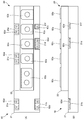
- FIG. 4 is a plan view of a plurality of ceramic circuit boards connected by a lead frame included in the semiconductor device of the first embodiment.
- FIG. 4 is a plan view of a plurality of ceramic circuit boards connected by a lead frame included in the semiconductor device of the first embodiment.
- FIG. 5 is a side view of a plurality of ceramic circuit boards connected by a lead frame included in the semiconductor device of the first embodiment.
- the description of the heat dissipation base plate 30 is omitted.
- FIG. 5 shows the side surface of the positive electrode lead frame 60a only. Further, FIG. 5 shows a part of the upper storage portion 22 of the case 20.
- the positive electrode lead frame 60a includes a main body portion 61, a positive electrode external connection terminal 62a, a linking portion 63, and a leg portion 64.
- the positive electrode lead frame 60a is provided with a leg portion 64 (and a linking portion 63) at a position corresponding to the ceramic circuit board 40 to be connected to the main body portion 61.
- the positive electrode lead frame 60a is provided with a positive electrode external connection terminal 62a with respect to the main body 61 according to the position exposed from the case 20.
- the lead frames 60b and 60c for the negative electrode and the output are also provided with the leg portions 64 (and the linking portion 63) at positions corresponding to the ceramic circuit board 40 to be connected to the main body portion 61.
- the lead frames 60b and 60c for the negative electrode and the output are for the negative electrode, which are not shown in FIGS. 4 and 5, depending on the positions exposed from the case 20 with respect to the main body 61 as shown in FIG. It is provided with external connection terminals 62b and 62c for output.
- the main body 61 has a flat plate shape, and as shown in FIGS. 4 and 5, a plurality of ceramic circuit boards 40 arranged in one direction are extended from the front surface to a predetermined height in the wiring direction. It is provided.
- the positive electrode, negative electrode, and output external connection terminals 62a to 62c are flat plates, project vertically with respect to the front surface of the ceramic circuit board 40, and are integrally connected to the main body 61. ..
- the positive electrode, negative electrode, and output external connection terminals 62a to 62c are provided so as to face the front surface of the upper storage portion 22 of the case 20, respectively.
- the positive electrode, negative electrode, and output external connection terminals 62a to 62c extend vertically from the front surface of the upper storage portion 22 of the case 20.
- the external connection terminals 62a to 62c for the positive electrode, the negative electrode, and the output extending from the front surface of the upper storage portion 22 of the case 20, as shown in FIG. 2, the positive electrode, the negative electrode, and the output
- the main surface of the external connection terminals 62a to 62c is exposed on the front surface of the upper storage portion 22.
- the leg portions 64 are electrically connected to the circuit patterns 42a to 42c of each ceramic circuit board 40 for each of the positive electrode, negative electrode, and output lead frames 60a to 60c. The details of the leg portion 64 will be described later.
- the linking portion 63 is integrally connected to the main body portion 61 and the leg portion 64. Therefore, the linking portion 63 electrically connects the main body portion 61 and the leg portion 64.
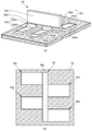
- FIG. 6 is a perspective view of a leg portion of a lead frame included in the semiconductor device of the first embodiment. Note that FIG. 6 shows the leg portion 64 (lower end portion side) of the lead frame 60, which is joined to the circuit pattern 42. In the lead frame 60, the main body portion 61 and the linking portion 63 are not shown.
- the leg portion 64 includes a vertical portion 64a and a split portion 64b, 64c.
- the width of the leg portion 64 is uniform in the vertical portion 64a and the divided portions 64b, 64c.
- the thickness of the divided portions 64b and 64c is approximately half the thickness of the vertical portion 64a, respectively. That is, the thickness of the vertical portion 64a is obtained by matching the thicknesses of the divided portions 64b and 64c.
- the vertical portion 64a extends in the vertical direction with respect to the circuit pattern 42.
- the vertical portion 64a is connected to the linking portion 63 at the stretching destination.
- the split portion 64b further includes a continuation portion 64b1 and a parallel portion 64b2.
- the continuation portion 64b1 bends in a predetermined direction from the branch portion 64a1 at the lower end portion of the vertical portion 64a on the circuit pattern 42 side.
- the predetermined direction is the thickness direction.
- the predetermined direction is divided so as to be split from a rift formed so as to cross the other end in parallel with the width direction at the other end of the sandwiched one end (vertical portion 64a) as described later.
- the parallel portion 64b2 is continuously extended from the continuation portion 64b1 in parallel with the circuit pattern 42, and is joined to the circuit pattern 42 by the circuit pattern joining region 64b3 on the back surface.
- the split portion 64c is provided on the opposite side of the split portion 64b and includes a continuation portion 64c1 and a parallel portion 64c2.
- the continuation portion 64c1 bends from the branch portion 64a1 at the lower end portion of the vertical portion 64a on the circuit pattern 42 side to the opposite side in a predetermined direction.
- the parallel portion 64c2 is continuously extended from the continuation portion 64c1 in parallel with the circuit pattern 42, and is joined to the circuit pattern 42 by the circuit pattern joining region 64c3 on the back surface.
- Such a leg portion 64 is attached to the circuit pattern 42 via a linking portion 63 with respect to the main body portion 61 so that a predetermined direction in the divided portions 64b and 64c is parallel to the wiring direction of the main body portion 61. ..
- the length from the branch portion 64a1 of the split portion 64b to the tip portion in the predetermined direction is equal to the length from the branch portion 64a1 of the split portion 64c to the tip portion on the opposite side in the predetermined direction.
- the widths of the divided portions 64b and 64c are the same, the areas of the divided portions 64b and 64c are equal, and in particular, the areas of the parallel portions 64b2 and 64c2 are equal.
- such a leg portion 64 sandwiches and fixes one end portion (vertical portion 64a) of a rectangular and plate-shaped conductive plate, and crosses the width parallel to the other end portion in the width direction.
- Form a rift It is obtained by dividing the crevice so as to be split and bending the divided pieces in opposite directions. Therefore, the thickness of the vertical portion 64a is the total thickness of the divided portions 64b and 64c. At this time, it is desirable that the thickness of the divided portions 64b and 64c is half the thickness of the vertical portions 64a, respectively.
- the divided portions 64b and 64c are joined to the circuit pattern 42. As will be described later, the divided portions 64b and 64c are bonded to the circuit pattern 42 by ultrasonic bonding.
- the leg portion 64 is stably joined to the circuit pattern 42.
- the vertical portion 64a is reliably and stably supported by the split portions 64b and 64c on the front surface side and the back surface side, respectively.
- the continuation portions 64b1 and 64c1 are not joined to the circuit pattern 42, and elasticity is exhibited between the vertical portion 64a and the division portions 64b and 64c. Therefore, the continuation portions 64b1 and 64c1 can alleviate the impact from the outside on the leg portions 64. Therefore, deformation, misalignment, and the like of the vertical portion 64a are prevented, and the lead frame 60 can be maintained at a predetermined joint location.
- FIG. 7 is a flowchart showing a method of manufacturing the semiconductor device according to the first embodiment.
- FIG. 8 is a diagram for explaining an ultrasonic bonding step included in the method for manufacturing a semiconductor device according to the first embodiment.
- Step S10 in FIG. 7 a preparation step of preparing a case 20, a heat dissipation base plate 30, a ceramic circuit board 40, control wiring units 50a to 50e, first semiconductor chips 45a and 46a and second semiconductor chips 45b and 46b, a lead frame 60, and the like is performed ( Step S10 in FIG. 7).
- the lead frame 60 is formed with the leg portion 64 shown in FIG. 6 in advance.
- step S11 in FIG. 7 The ceramic circuit board 40 and the control wiring units 50a to 50e are placed on the front surface of the heat dissipation base plate 30 via solder. Further, the first semiconductor chips 45a and 46a and the second semiconductor chips 45b and 46b are placed on the circuit pattern 42 of the ceramic circuit board 40 via solder, respectively.
- step S11 step S12 in FIG. 7
- it is heated to melt the solder.
- the solder After the solder has melted, it is cooled to solidify the solder, so that the ceramic circuit board 40 and the control wiring units 50a to 50e are joined to the heat dissipation base plate 30 by solder, respectively.
- the first semiconductor chips 45a and 46a and the second semiconductor chips 45b and 46b are joined to the circuit pattern 42 of the ceramic circuit board 40 by soldering, respectively.
- a wiring step is performed in which the ceramic circuit board 40 is electrically connected to the first semiconductor chips 45a, 46a and the second semiconductor chips 45b, 46b by a bonding wire, and wiring is performed (step S13 in FIG. 7). ).
- an ultrasonic bonding step of bonding the leg portion 64 of the lead frame 60 to the circuit pattern 42 of the ceramic circuit board 40 by ultrasonic bonding is performed (step S14 in FIG. 7). Ultrasonic bonding is performed by an ultrasonic bonding device.
- the ultrasonic bonding apparatus includes an ultrasonic generator and an ultrasonic tool 70, which is shown in FIG. 8, for propagating ultrasonic waves generated from the ultrasonic generator.
- the circuit pattern joining regions 64b3 and 64c3 of the parallel portions 64b2 and 64c2 of the leg portions 64 are arranged at the joining portions of the circuit pattern 42.
- Two ultrasonic tools 70 of the ultrasonic bonding device are set in parallel portions 64b2 and 64c2 of the leg portion 64, respectively, as shown in FIG.
- the ultrasonic tool 70 has an L-shape and includes a pressing portion 71 and a propagation portion 72 connected to the pressing portion 71.
- the pressing portion 71 includes a flat surface abutting on the front side of the parallel portions 64b2 and 64c2 of the leg portion 64.
- the propagation portion 72 is provided with a pressing portion 71 on one end side thereof, and the other end side is connected to the ultrasonic wave generator.
- the propagation unit 72 propagates the ultrasonic vibration generated from the ultrasonic wave generator to the pressing unit 71.
- the pressing portion 71 of the ultrasonic tool 70 presses the parallel portions 64b2, 64c2 of the leg portion 64 while simultaneously vibrating against the circuit pattern 42. Then, the parallel portions 64b2 and 64c2 are simultaneously deformed by ultrasonic vibration and parallel to the vibration direction (for example, the bending direction of the divided portions 64b and 64c) (for example, the arrow direction of the broken line in FIG. 8). That is, since the parallel portions 64b2 and 64c2 are similarly deformed along the vibration direction, the parallel portions 64b2 and 64c2 can be joined to the circuit pattern 42 without the vertical portions 64a being displaced.
- the lead frame 60 is appropriately bonded to a predetermined bonding portion of the plurality of ceramic circuit boards 40.
- the parallel portions 64b2 and 64c2 of the leg portions 64 may be pressed and joined by the pressing portion 71 of the ultrasonic tool 70 as follows. That is, in the lead frame 60 provided with the plurality of leg portions 64, the parallel portions 64b2, 64c2 are provided along the main end portion 61 from the leg portion 64 at one end to the leg portion 64 at the other end by the ultrasonic tool 71. It may be alternately ultrasonically bonded to the ceramic circuit substrate 40.
- the parallel portion 64b2 of the leg portion 64 at the end of the positive electrode lead frame 60a is bonded to the ceramic circuit board 40a by ultrasonic bonding, and the parallel portion 64c2 of the leg portion 64 is bonded to the ceramic circuit board 40a by ultrasonic bonding.
- the parallel portion 64b2 of the leg portion 64 adjacent to the leg portion 64 at the end of the positive electrode lead frame 60a is bonded to the ceramic circuit board 40b by ultrasonic bonding
- the parallel portion 64c2 of the leg portion 64 is bonded to the ceramic circuit. It is bonded to the substrate 40b by ultrasonic bonding.
- the leg portions 64 are joined to the ceramic circuit board 40 in the order of parallel portions 64b and 64c2 along the main body portion 61.
- the parallel portion 64b2 of the leg portion 64 at the final end of the positive electrode lead frame 60a is bonded to the ceramic circuit board 40f by ultrasonic bonding, and the parallel portion 64c2 of the leg portion 64 is ultrasonically bonded to the ceramic circuit board 40f. Bond by. It should be noted that not only when the parallel portions 64b2, 64c2 of the plurality of leg portions 64 are alternately joined along the main body portion 61 of the lead frame 60, the parallel portions 64c2, 64b2 of the plurality of leg portions 64 along the main body portion 61 are not limited. May be joined alternately.
- the legs 64 provided on the lead frame 60 are joined in order from the ceramic circuit board 40a toward the ceramic circuit board 40f, as in the case where the parallel portions 64b2 and 64c2 of the legs 64 are joined at the same time.
- the misalignment of the leg portion 64 of the lead frame 60 does not increase as it approaches the ceramic circuit board 40f. Therefore, the lead frame 60 is appropriately bonded to a predetermined bonding portion of the plurality of ceramic circuit boards 40.
- the positive electrode, negative electrode, output, and control external connection terminals 62a to 62d are exposed from each position of the case 20, and the case 20 is attached to the heat dissipation base plate 30 with an adhesive (step S15 in FIG. 7). .. As a result, the semiconductor device 10 shown in FIG. 2 is obtained.
- the semiconductor device 10 is provided on the first semiconductor chips 45a, 46a, the second semiconductor chips 45b, 46b, the insulating plate 41, and the insulating plate 41, and the first semiconductor chips 45a, 46a and the second semiconductor chips 45b, 46b.
- a ceramic circuit board 40 having a circuit pattern 42 electrically connected to and.
- the semiconductor device 10 includes a lead frame 60 having a leg portion 64 to which a circuit pattern 42 is bonded at one end and external connection terminals 62a to 62c for positive electrodes, negative electrodes, and outputs at the other end.
- the leg portion 64 further includes a vertical portion 64a and a split portion 64b, 64c.
- the vertical portion 64a extends in the vertical direction with respect to the circuit pattern 42.
- the split portion 64b is bent in a predetermined direction from the branch portion 64a1 at the lower end of the vertical portion 64a on the circuit pattern 42 side, extends parallel to the circuit pattern 42, and is joined to the circuit pattern 42.
- the divided portion 64c is bent from the branched portion 64a1 in the opposite direction in a predetermined direction, extends in parallel with the circuit pattern 42, and is joined to the circuit pattern 42.
- leg portion 64 In such a leg portion 64, the vertical portion 64a is reliably supported by the front surface side and the back surface side by the divided portions 64b and 64c, respectively. Therefore, the leg portion 64 is stably joined to the circuit pattern 42. Further, since the leg portion 64 is divided in the thickness direction, the divided portions 64b and 64c are thinner than the vertical portion 64a, and the joint portions 64b3 between the parallel portions 64b and 64c and the circuit pattern 42 are formed. Ultrasonic vibration is easily transmitted to 64c3, and it is possible to bond more firmly. Further, such leg portions 64 are simultaneously joined to the circuit pattern 42 by dividing portions 64b and 64c by ultrasonic vibration.
- the semiconductor device 10 can be appropriately manufactured.
- FIG. 9 is a perspective view of a leg portion of a lead frame included in the semiconductor device of the second embodiment. Note that FIG. 9 shows only the leg portion 64. The leg portion 64 of the second embodiment is provided in place of the leg portion 64 of the lead frame 60 of the first embodiment. Therefore, other configurations of the semiconductor device of the second embodiment have the same configuration as that of the semiconductor device 10 of the first embodiment.
- the leg portion 64 shown in FIG. 9 includes a vertical portion 64a and a split portion 64b, 64c.
- the vertical portion 64a extends in the vertical direction with respect to the circuit pattern 42.
- the vertical portion 64a is connected to the linking portion 63 at the stretching destination.
- the divided portions 64b and 64c are cut and divided at one place perpendicular to the vertical portion 64a with respect to the width direction of the vertical portion 64a. Therefore, the combined width of the divided portions 64b and 64c corresponds to the width of the vertical portion 64a.
- the split portion 64b further includes a continuation portion 64b1 and a parallel portion 64b2.
- the continuation portion 64b1 bends in a predetermined direction from the branch portion 64a1 at the lower end portion of the vertical portion 64a on the circuit pattern 42 side, as in the first embodiment.
- the parallel portion 64b2 is continuously extended from the continuation portion 64b1 in parallel with the circuit pattern 42, and is joined to the circuit pattern 42 by the circuit pattern joining region 64b3 on the back surface.
- the split portion 64c is provided on the opposite side of the split portion 64b and includes a continuation portion 64c1 and a parallel portion 64c2.
- the continuation portion 64c1 bends from the branch portion 64a1 at the lower end portion of the vertical portion 64a on the circuit pattern 42 side to the opposite side in a predetermined direction.
- the parallel portion 64c2 is continuously extended from the continuation portion 64c1 in parallel with the circuit pattern 42, and is joined to the circuit pattern 42 by the circuit pattern joining region 64c3 on the back surface. Further, in such a leg portion 64, as in the first embodiment, the parallel portion 64b2, 64c2 of the leg portion 64 is first implemented with respect to the circuit pattern 42 by the pressing portion 71 of the ultrasonic tool 70. It can be joined by pressing while vibrating at the same time or alternately vibrating in the same manner as in the above form.
- Such a leg portion 64 is also attached to the circuit pattern 42 so that a predetermined direction in the divided portions 64b and 64c is parallel to the wiring direction of the main body portion 61 via the linking portion 63 with respect to the main body portion 61.
- the length from the branch portion 64a1 of the split portion 64b to the tip portion in the predetermined direction is equal to the length from the branch portion 64a1 of the split portion 64c to the tip portion on the opposite side in the predetermined direction.
- the divided portions 64b and 64c are divided at the center of the width of the vertical portion 64a, the respective widths are the same, so that the areas of the divided portions 64b and 64c are the same, and in particular, the areas of the parallel portions 64b2 and 64c2. Are equal.
- FIG. 10 is a diagram for explaining another leg of a lead frame included in the semiconductor device of the second embodiment.
- 10 (A) shows a perspective view of the leg portion 64
- FIG. 10 (B) shows a plan view of the leg portion 64.
- the divided portion 64c is not shown, but is arranged on the back side of the vertical portion 64a.
- the leg portion 64 shown in FIG. 10 includes a vertical portion 64a and a divided portion 64b to 64e.
- the vertical portion 64a extends in the vertical direction with respect to the circuit pattern 42.
- the vertical portion 64a is connected to the linking portion 63 at the stretching destination.
- the divided portions 64b to 64e are perpendicular to the vertical portion 64a with respect to the width direction of the vertical portion 64a and are cut and divided at three points at equal intervals. Therefore, the combined width of the divided portions 64b to 64e corresponds to the width of the vertical portion 64a. That is, the leg portion 64 shown in FIG. 10 includes two sets of the divided portions 64b and 64c of the leg portion 64 shown in FIG.
- the leg portion 64 shown in FIG. 10 is not limited to the case where two sets of the leg portions 64 shown in FIG. 9 are included, and may include three or more sets.
- the split portion 64b further includes a continuation portion 64b1 and a parallel portion 64b2.
- the continuation portion 64b1 bends in a predetermined direction from the branch portion 64a1 at the lower end portion of the vertical portion 64a on the circuit pattern 42 side.
- the parallel portion 64b2 is continuously extended from the continuation portion 64b1 in parallel with the circuit pattern 42, and is joined to the circuit pattern 42 by the circuit pattern joining region 64b3 on the back surface.
- the divided portion 64d also includes a continuous portion 64d1 and a parallel portion 64d2.
- the continuation portion 64d1 bends in a predetermined direction from the branch portion 64a1 at the lower end portion of the vertical portion 64a on the circuit pattern 42 side.
- the parallel portion 64d2 is continuously extended from the continuation portion 64d1 in parallel with the circuit pattern 42, and is joined to the circuit pattern 42 by the circuit pattern joining region 64d3 on the back surface.
- the divided portion 64c is provided on the opposite side of the divided portions 64b and 64d of the vertical portion 64a, and includes a continuous portion 64c1 and a parallel portion 64c2 (see FIG. 9).
- the continuation portion 64c1 bends from the branch portion 64a1 at the lower end portion of the vertical portion 64a on the circuit pattern 42 side to the opposite side of the continuation portion 64b1.
- the parallel portion 64c2 is continuously extended from the continuation portion 64c1 in parallel with the circuit pattern 42, and is joined to the circuit pattern 42 by the circuit pattern joining region 64c3 on the back surface.
- the split portion 64e is provided on the opposite side of the split portions 64b and 64d of the vertical portion 64a, and includes a continuation portion 64e1 and a parallel portion 64e2.
- the continuation portion 64e1 bends from the branch portion 64a1 at the lower end portion of the vertical portion 64a on the circuit pattern 42 side to the opposite side in a predetermined direction.
- the parallel portion 64e2 is continuously extended from the continuation portion 64e1 in parallel with the circuit pattern 42, and is joined to the circuit pattern 42 by the circuit pattern joining region 64e3 on the back surface.
- Such a leg portion 64 is also attached to the circuit pattern 42 via a linking portion 63 with respect to the main body portion 61 so that a predetermined direction in the divided portions 64b to 64e is parallel to the wiring direction of the main body portion 61.
- the length from the branch portion 64a1 of the split portion 64b to the tip portion in the predetermined direction, the length from the branch portion 64a1 of the split portion 64c to the tip portion on the opposite side in the predetermined direction, and the branch portion of the split portion 64d is equal to the length from the branch portion 64a1 of the split portion 64e to the tip on the opposite side in the predetermined direction.
- the divided portions 64b to 64e are divided into three at equal intervals with respect to the width of the vertical portion 6a, and since the respective widths are the same, the areas of the divided portions 64b to 64e are the same, and in particular, the parallel portions 64b2 to 64e2. The areas are equal.
- Such a leg portion 64 can also be joined to the circuit pattern 42 by the pressing portion 71 of the ultrasonic tool 70, as in the first embodiment.
- the ultrasonic tool 70 is prepared corresponding to the divided portions 64b to 64e of the leg portion 64, and the divided portions 64b to 64e are joined by simultaneously vibrating and pressing against the circuit pattern 42. Can be done.
- the vertical portion 64a is surely divided into the front surface side and the back surface side by the divided portions 64b and 64c (64b to 64e), respectively. Be supported. Therefore, the leg portion 64 is stably joined to the circuit pattern 42. Further, such leg portions 64 are simultaneously joined to the circuit pattern 42 by dividing portions 64b and 64c (64b to 64e) by ultrasonic vibration. Then, since the divided portions 64b and 64c (64b to 64e) are similarly deformed in parallel with the bending direction, the vertical portion 64a does not shift in position. Therefore, the positional deviation of the vertical portion 64a is prevented, and the lead frame 60 can be maintained at a predetermined joint location. As a result, the semiconductor device can be appropriately manufactured.
Landscapes
- Engineering & Computer Science (AREA)
- Microelectronics & Electronic Packaging (AREA)
- Manufacturing & Machinery (AREA)
- Physics & Mathematics (AREA)
- Thermal Sciences (AREA)
- Lead Frames For Integrated Circuits (AREA)
- Electric Connection Of Electric Components To Printed Circuits (AREA)
- Structures For Mounting Electric Components On Printed Circuit Boards (AREA)
- Cooling Or The Like Of Semiconductors Or Solid State Devices (AREA)
Priority Applications (4)
| Application Number | Priority Date | Filing Date | Title |
|---|---|---|---|
| DE112021000211.2T DE112021000211B4 (de) | 2020-07-09 | 2021-05-28 | Halbleitervorrichtung und Verfahren zum Herstellen derselben |
| JP2022534946A JP7428254B2 (ja) | 2020-07-09 | 2021-05-28 | 半導体装置及び半導体装置の製造方法 |
| CN202180007987.8A CN114902389B (zh) | 2020-07-09 | 2021-05-28 | 半导体装置以及半导体装置的制造方法 |
| US17/855,162 US20220330429A1 (en) | 2020-07-09 | 2022-06-30 | Semiconductor device and method of manufacturing the same |
Applications Claiming Priority (2)
| Application Number | Priority Date | Filing Date | Title |
|---|---|---|---|
| JP2020-118648 | 2020-07-09 | ||
| JP2020118648 | 2020-07-09 |
Related Child Applications (1)
| Application Number | Title | Priority Date | Filing Date |
|---|---|---|---|
| US17/855,162 Continuation US20220330429A1 (en) | 2020-07-09 | 2022-06-30 | Semiconductor device and method of manufacturing the same |
Publications (1)
| Publication Number | Publication Date |
|---|---|
| WO2022009556A1 true WO2022009556A1 (ja) | 2022-01-13 |
Family
ID=79552333
Family Applications (1)
| Application Number | Title | Priority Date | Filing Date |
|---|---|---|---|
| PCT/JP2021/020530 Ceased WO2022009556A1 (ja) | 2020-07-09 | 2021-05-28 | 半導体装置及び半導体装置の製造方法 |
Country Status (5)
| Country | Link |
|---|---|
| US (1) | US20220330429A1 (https=) |
| JP (1) | JP7428254B2 (https=) |
| CN (1) | CN114902389B (https=) |
| DE (1) | DE112021000211B4 (https=) |
| WO (1) | WO2022009556A1 (https=) |
Cited By (1)
| Publication number | Priority date | Publication date | Assignee | Title |
|---|---|---|---|---|
| JP2023168849A (ja) * | 2022-05-16 | 2023-11-29 | 富士電機株式会社 | 半導体装置、及び、半導体装置の製造方法 |
Citations (2)
| Publication number | Priority date | Publication date | Assignee | Title |
|---|---|---|---|---|
| WO2016031020A1 (ja) * | 2014-08-28 | 2016-03-03 | 三菱電機株式会社 | 半導体装置 |
| WO2019230292A1 (ja) * | 2018-06-01 | 2019-12-05 | 富士電機株式会社 | 半導体装置 |
Family Cites Families (7)
| Publication number | Priority date | Publication date | Assignee | Title |
|---|---|---|---|---|
| JP3895465B2 (ja) * | 1998-05-14 | 2007-03-22 | 沖電気工業株式会社 | 基板の実装方法、基板の実装構造 |
| JP4537370B2 (ja) * | 2006-12-04 | 2010-09-01 | 日立オートモティブシステムズ株式会社 | 電子装置 |
| JP5555206B2 (ja) * | 2011-07-11 | 2014-07-23 | 株式会社 日立パワーデバイス | 半導体パワーモジュール |
| JPWO2017002268A1 (ja) * | 2015-07-02 | 2017-10-19 | ルネサスエレクトロニクス株式会社 | 半導体装置の製造方法および半導体装置 |
| JP6755197B2 (ja) * | 2017-01-19 | 2020-09-16 | 三菱電機株式会社 | 半導体装置およびその製造方法 |
| DE102018204408B4 (de) * | 2018-03-22 | 2022-05-05 | Danfoss Silicon Power Gmbh | Stromschiene, verfahren zum herstellen derselben und leistungsmodul, welches eine solche aufweist |
| US10862232B2 (en) * | 2018-08-02 | 2020-12-08 | Dell Products L.P. | Circuit board pad connector system |
-
2021
- 2021-05-28 CN CN202180007987.8A patent/CN114902389B/zh active Active
- 2021-05-28 JP JP2022534946A patent/JP7428254B2/ja active Active
- 2021-05-28 DE DE112021000211.2T patent/DE112021000211B4/de active Active
- 2021-05-28 WO PCT/JP2021/020530 patent/WO2022009556A1/ja not_active Ceased
-
2022
- 2022-06-30 US US17/855,162 patent/US20220330429A1/en active Pending
Patent Citations (2)
| Publication number | Priority date | Publication date | Assignee | Title |
|---|---|---|---|---|
| WO2016031020A1 (ja) * | 2014-08-28 | 2016-03-03 | 三菱電機株式会社 | 半導体装置 |
| WO2019230292A1 (ja) * | 2018-06-01 | 2019-12-05 | 富士電機株式会社 | 半導体装置 |
Cited By (1)
| Publication number | Priority date | Publication date | Assignee | Title |
|---|---|---|---|---|
| JP2023168849A (ja) * | 2022-05-16 | 2023-11-29 | 富士電機株式会社 | 半導体装置、及び、半導体装置の製造方法 |
Also Published As
| Publication number | Publication date |
|---|---|
| JPWO2022009556A1 (https=) | 2022-01-13 |
| DE112021000211B4 (de) | 2025-08-21 |
| JP7428254B2 (ja) | 2024-02-06 |
| DE112021000211T5 (de) | 2022-08-18 |
| CN114902389A (zh) | 2022-08-12 |
| US20220330429A1 (en) | 2022-10-13 |
| CN114902389B (zh) | 2026-02-06 |
Similar Documents
| Publication | Publication Date | Title |
|---|---|---|
| CN102881682B (zh) | 半导体功率模块 | |
| CN107615464B (zh) | 电力用半导体装置的制造方法以及电力用半导体装置 | |
| CN104821282A (zh) | 功率半导体组件 | |
| KR20120127535A (ko) | 프레스 피트 단자 및 반도체 장치 | |
| CN112786556B (zh) | 半导体装置及半导体装置的制造方法 | |
| JP7459465B2 (ja) | 半導体装置及び半導体装置の製造方法 | |
| JP2021090030A (ja) | 半導体装置及び半導体装置の製造方法 | |
| JP2019054137A (ja) | ウェッジツール及びウェッジボンディング方法 | |
| JP2020136449A (ja) | 半導体装置の製造方法 | |
| JP7428254B2 (ja) | 半導体装置及び半導体装置の製造方法 | |
| JP2019083292A (ja) | 半導体装置 | |
| CN116913904A (zh) | 半导体模块 | |
| JP7201106B2 (ja) | 半導体装置 | |
| JP4586508B2 (ja) | 半導体装置およびその製造方法 | |
| JP7736105B2 (ja) | 半導体ユニット及び半導体装置 | |
| JP7490974B2 (ja) | 半導体モジュール及び半導体モジュールの製造方法 | |
| JPWO2022009556A5 (https=) | ||
| JP2021044452A (ja) | 半導体装置 | |
| JP7562953B2 (ja) | 半導体モジュール | |
| JP2024076763A (ja) | 電子装置及び電子装置の製造方法 | |
| JP2023183648A (ja) | 電力変換装置及び電力変換装置の製造方法 | |
| JP7342889B2 (ja) | 半導体装置 | |
| US20250279339A1 (en) | Semiconductor device and external connection main terminal | |
| US20250079383A1 (en) | Semiconductor device | |
| US20240304530A1 (en) | Power converter apparatus |
Legal Events
| Date | Code | Title | Description |
|---|---|---|---|
| 121 | Ep: the epo has been informed by wipo that ep was designated in this application |
Ref document number: 21838264 Country of ref document: EP Kind code of ref document: A1 |
|
| ENP | Entry into the national phase |
Ref document number: 2022534946 Country of ref document: JP Kind code of ref document: A |
|
| 122 | Ep: pct application non-entry in european phase |
Ref document number: 21838264 Country of ref document: EP Kind code of ref document: A1 |
|
| WWG | Wipo information: grant in national office |
Ref document number: 112021000211 Country of ref document: DE |