WO2022009556A1 - 半導体装置及び半導体装置の製造方法 - Google Patents
半導体装置及び半導体装置の製造方法 Download PDFInfo
- Publication number
- WO2022009556A1 WO2022009556A1 PCT/JP2021/020530 JP2021020530W WO2022009556A1 WO 2022009556 A1 WO2022009556 A1 WO 2022009556A1 JP 2021020530 W JP2021020530 W JP 2021020530W WO 2022009556 A1 WO2022009556 A1 WO 2022009556A1
- Authority
- WO
- WIPO (PCT)
- Prior art keywords
- circuit pattern
- semiconductor device
- joined
- divided
- legs
- Prior art date
Links
- 239000004065 semiconductor Substances 0.000 title claims description 114
- 238000004519 manufacturing process Methods 0.000 title claims description 13
- 238000000034 method Methods 0.000 title claims description 11
- 238000005452 bending Methods 0.000 claims description 7
- 238000002360 preparation method Methods 0.000 claims description 3
- 239000000919 ceramic Substances 0.000 description 71
- 230000017525 heat dissipation Effects 0.000 description 25
- PXHVJJICTQNCMI-UHFFFAOYSA-N Nickel Chemical compound [Ni] PXHVJJICTQNCMI-UHFFFAOYSA-N 0.000 description 20
- 238000003860 storage Methods 0.000 description 19
- 229910052751 metal Inorganic materials 0.000 description 18
- 239000002184 metal Substances 0.000 description 18
- 238000005304 joining Methods 0.000 description 16
- 229910000679 solder Inorganic materials 0.000 description 16
- 238000003825 pressing Methods 0.000 description 12
- 229910045601 alloy Inorganic materials 0.000 description 11
- 239000000956 alloy Substances 0.000 description 11
- 229910052802 copper Inorganic materials 0.000 description 10
- 239000010949 copper Substances 0.000 description 10
- 229910052759 nickel Inorganic materials 0.000 description 10
- RYGMFSIKBFXOCR-UHFFFAOYSA-N Copper Chemical compound [Cu] RYGMFSIKBFXOCR-UHFFFAOYSA-N 0.000 description 9
- XEEYBQQBJWHFJM-UHFFFAOYSA-N Iron Chemical compound [Fe] XEEYBQQBJWHFJM-UHFFFAOYSA-N 0.000 description 8
- BQCADISMDOOEFD-UHFFFAOYSA-N Silver Chemical compound [Ag] BQCADISMDOOEFD-UHFFFAOYSA-N 0.000 description 8
- 239000000463 material Substances 0.000 description 8
- 229910052709 silver Inorganic materials 0.000 description 8
- 239000004332 silver Substances 0.000 description 8
- 229910000521 B alloy Inorganic materials 0.000 description 5
- 229910001096 P alloy Inorganic materials 0.000 description 5
- 229910052782 aluminium Inorganic materials 0.000 description 5
- XAGFODPZIPBFFR-UHFFFAOYSA-N aluminium Chemical compound [Al] XAGFODPZIPBFFR-UHFFFAOYSA-N 0.000 description 5
- QDWJUBJKEHXSMT-UHFFFAOYSA-N boranylidynenickel Chemical compound [Ni]#B QDWJUBJKEHXSMT-UHFFFAOYSA-N 0.000 description 5
- 238000005260 corrosion Methods 0.000 description 5
- 230000007797 corrosion Effects 0.000 description 5
- OFNHPGDEEMZPFG-UHFFFAOYSA-N phosphanylidynenickel Chemical compound [P].[Ni] OFNHPGDEEMZPFG-UHFFFAOYSA-N 0.000 description 5
- 238000007747 plating Methods 0.000 description 5
- 229920005989 resin Polymers 0.000 description 5
- 239000011347 resin Substances 0.000 description 5
- 229910052742 iron Inorganic materials 0.000 description 4
- 239000000758 substrate Substances 0.000 description 4
- 239000000654 additive Substances 0.000 description 3
- 238000010586 diagram Methods 0.000 description 3
- 150000002739 metals Chemical class 0.000 description 3
- 238000012986 modification Methods 0.000 description 3
- 230000004048 modification Effects 0.000 description 3
- TWNQGVIAIRXVLR-UHFFFAOYSA-N oxo(oxoalumanyloxy)alumane Chemical compound O=[Al]O[Al]=O TWNQGVIAIRXVLR-UHFFFAOYSA-N 0.000 description 3
- 229910052710 silicon Inorganic materials 0.000 description 3
- 239000010703 silicon Substances 0.000 description 3
- 229910000881 Cu alloy Inorganic materials 0.000 description 2
- 229910052581 Si3N4 Inorganic materials 0.000 description 2
- 238000013459 approach Methods 0.000 description 2
- 239000004519 grease Substances 0.000 description 2
- 229910044991 metal oxide Inorganic materials 0.000 description 2
- 150000004706 metal oxides Chemical class 0.000 description 2
- -1 polybutylene terephthalate Polymers 0.000 description 2
- HBMJWWWQQXIZIP-UHFFFAOYSA-N silicon carbide Chemical compound [Si+]#[C-] HBMJWWWQQXIZIP-UHFFFAOYSA-N 0.000 description 2
- 229910010271 silicon carbide Inorganic materials 0.000 description 2
- HQVNEWCFYHHQES-UHFFFAOYSA-N silicon nitride Chemical compound N12[Si]34N5[Si]62N3[Si]51N64 HQVNEWCFYHHQES-UHFFFAOYSA-N 0.000 description 2
- 238000005476 soldering Methods 0.000 description 2
- 239000004734 Polyphenylene sulfide Substances 0.000 description 1
- XUIMIQQOPSSXEZ-UHFFFAOYSA-N Silicon Chemical compound [Si] XUIMIQQOPSSXEZ-UHFFFAOYSA-N 0.000 description 1
- QLTBJHSQPNVBLW-UHFFFAOYSA-N [Bi].[In].[Ag].[Sn] Chemical compound [Bi].[In].[Ag].[Sn] QLTBJHSQPNVBLW-UHFFFAOYSA-N 0.000 description 1
- JVCDUTIVKYCTFB-UHFFFAOYSA-N [Bi].[Zn].[Sn] Chemical compound [Bi].[Zn].[Sn] JVCDUTIVKYCTFB-UHFFFAOYSA-N 0.000 description 1
- PQIJHIWFHSVPMH-UHFFFAOYSA-N [Cu].[Ag].[Sn] Chemical compound [Cu].[Ag].[Sn] PQIJHIWFHSVPMH-UHFFFAOYSA-N 0.000 description 1
- XECAHXYUAAWDEL-UHFFFAOYSA-N acrylonitrile butadiene styrene Chemical compound C=CC=C.C=CC#N.C=CC1=CC=CC=C1 XECAHXYUAAWDEL-UHFFFAOYSA-N 0.000 description 1
- 229920000122 acrylonitrile butadiene styrene Polymers 0.000 description 1
- 239000004676 acrylonitrile butadiene styrene Substances 0.000 description 1
- 239000000853 adhesive Substances 0.000 description 1
- 230000001070 adhesive effect Effects 0.000 description 1
- 230000004888 barrier function Effects 0.000 description 1
- 238000005219 brazing Methods 0.000 description 1
- 229910017052 cobalt Inorganic materials 0.000 description 1
- 239000010941 cobalt Substances 0.000 description 1
- GUTLYIVDDKVIGB-UHFFFAOYSA-N cobalt atom Chemical compound [Co] GUTLYIVDDKVIGB-UHFFFAOYSA-N 0.000 description 1
- 239000002131 composite material Substances 0.000 description 1
- 238000001816 cooling Methods 0.000 description 1
- KUNSUQLRTQLHQQ-UHFFFAOYSA-N copper tin Chemical compound [Cu].[Sn] KUNSUQLRTQLHQQ-UHFFFAOYSA-N 0.000 description 1
- PMHQVHHXPFUNSP-UHFFFAOYSA-M copper(1+);methylsulfanylmethane;bromide Chemical compound Br[Cu].CSC PMHQVHHXPFUNSP-UHFFFAOYSA-M 0.000 description 1
- 238000005516 engineering process Methods 0.000 description 1
- 238000005530 etching Methods 0.000 description 1
- 230000005669 field effect Effects 0.000 description 1
- 239000000945 filler Substances 0.000 description 1
- 230000014509 gene expression Effects 0.000 description 1
- 229910052732 germanium Inorganic materials 0.000 description 1
- GNPVGFCGXDBREM-UHFFFAOYSA-N germanium atom Chemical compound [Ge] GNPVGFCGXDBREM-UHFFFAOYSA-N 0.000 description 1
- PCHJSUWPFVWCPO-UHFFFAOYSA-N gold Chemical compound [Au] PCHJSUWPFVWCPO-UHFFFAOYSA-N 0.000 description 1
- 229910052737 gold Inorganic materials 0.000 description 1
- 239000010931 gold Substances 0.000 description 1
- 230000005484 gravity Effects 0.000 description 1
- 238000009413 insulation Methods 0.000 description 1
- RVTZCBVAJQQJTK-UHFFFAOYSA-N oxygen(2-);zirconium(4+) Chemical compound [O-2].[O-2].[Zr+4] RVTZCBVAJQQJTK-UHFFFAOYSA-N 0.000 description 1
- 229920006122 polyamide resin Polymers 0.000 description 1
- 229920002961 polybutylene succinate Polymers 0.000 description 1
- 239000004631 polybutylene succinate Substances 0.000 description 1
- 229920001707 polybutylene terephthalate Polymers 0.000 description 1
- 229920000069 polyphenylene sulfide Polymers 0.000 description 1
- 229920001296 polysiloxane Polymers 0.000 description 1
- 230000001902 propagating effect Effects 0.000 description 1
- 229920005992 thermoplastic resin Polymers 0.000 description 1
- 229910000969 tin-silver-copper Inorganic materials 0.000 description 1
- 229910001928 zirconium oxide Inorganic materials 0.000 description 1
Images


Classifications
-
- H—ELECTRICITY
- H05—ELECTRIC TECHNIQUES NOT OTHERWISE PROVIDED FOR
- H05K—PRINTED CIRCUITS; CASINGS OR CONSTRUCTIONAL DETAILS OF ELECTRIC APPARATUS; MANUFACTURE OF ASSEMBLAGES OF ELECTRICAL COMPONENTS
- H05K1/00—Printed circuits
- H05K1/02—Details
- H05K1/11—Printed elements for providing electric connections to or between printed circuits
- H05K1/111—Pads for surface mounting, e.g. lay-out
-
- H—ELECTRICITY
- H01—ELECTRIC ELEMENTS
- H01L—SEMICONDUCTOR DEVICES NOT COVERED BY CLASS H10
- H01L25/00—Assemblies consisting of a plurality of individual semiconductor or other solid state devices ; Multistep manufacturing processes thereof
- H01L25/03—Assemblies consisting of a plurality of individual semiconductor or other solid state devices ; Multistep manufacturing processes thereof all the devices being of a type provided for in the same subgroup of groups H01L27/00 - H01L33/00, or in a single subclass of H10K, H10N, e.g. assemblies of rectifier diodes
- H01L25/04—Assemblies consisting of a plurality of individual semiconductor or other solid state devices ; Multistep manufacturing processes thereof all the devices being of a type provided for in the same subgroup of groups H01L27/00 - H01L33/00, or in a single subclass of H10K, H10N, e.g. assemblies of rectifier diodes the devices not having separate containers
- H01L25/07—Assemblies consisting of a plurality of individual semiconductor or other solid state devices ; Multistep manufacturing processes thereof all the devices being of a type provided for in the same subgroup of groups H01L27/00 - H01L33/00, or in a single subclass of H10K, H10N, e.g. assemblies of rectifier diodes the devices not having separate containers the devices being of a type provided for in group H01L29/00
- H01L25/072—Assemblies consisting of a plurality of individual semiconductor or other solid state devices ; Multistep manufacturing processes thereof all the devices being of a type provided for in the same subgroup of groups H01L27/00 - H01L33/00, or in a single subclass of H10K, H10N, e.g. assemblies of rectifier diodes the devices not having separate containers the devices being of a type provided for in group H01L29/00 the devices being arranged next to each other
-
- H—ELECTRICITY
- H01—ELECTRIC ELEMENTS
- H01L—SEMICONDUCTOR DEVICES NOT COVERED BY CLASS H10
- H01L21/00—Processes or apparatus adapted for the manufacture or treatment of semiconductor or solid state devices or of parts thereof
- H01L21/02—Manufacture or treatment of semiconductor devices or of parts thereof
- H01L21/04—Manufacture or treatment of semiconductor devices or of parts thereof the devices having potential barriers, e.g. a PN junction, depletion layer or carrier concentration layer
- H01L21/50—Assembly of semiconductor devices using processes or apparatus not provided for in a single one of the subgroups H01L21/06 - H01L21/326, e.g. sealing of a cap to a base of a container
- H01L21/60—Attaching or detaching leads or other conductive members, to be used for carrying current to or from the device in operation
- H01L21/607—Attaching or detaching leads or other conductive members, to be used for carrying current to or from the device in operation involving the application of mechanical vibrations, e.g. ultrasonic vibrations
-
- H—ELECTRICITY
- H01—ELECTRIC ELEMENTS
- H01L—SEMICONDUCTOR DEVICES NOT COVERED BY CLASS H10
- H01L23/00—Details of semiconductor or other solid state devices
- H01L23/48—Arrangements for conducting electric current to or from the solid state body in operation, e.g. leads, terminal arrangements ; Selection of materials therefor
- H01L23/488—Arrangements for conducting electric current to or from the solid state body in operation, e.g. leads, terminal arrangements ; Selection of materials therefor consisting of soldered or bonded constructions
- H01L23/498—Leads, i.e. metallisations or lead-frames on insulating substrates, e.g. chip carriers
- H01L23/49838—Geometry or layout
-
- H—ELECTRICITY
- H01—ELECTRIC ELEMENTS
- H01L—SEMICONDUCTOR DEVICES NOT COVERED BY CLASS H10
- H01L25/00—Assemblies consisting of a plurality of individual semiconductor or other solid state devices ; Multistep manufacturing processes thereof
- H01L25/18—Assemblies consisting of a plurality of individual semiconductor or other solid state devices ; Multistep manufacturing processes thereof the devices being of types provided for in two or more different subgroups of the same main group of groups H01L27/00 - H01L33/00, or in a single subclass of H10K, H10N
-
- H—ELECTRICITY
- H05—ELECTRIC TECHNIQUES NOT OTHERWISE PROVIDED FOR
- H05K—PRINTED CIRCUITS; CASINGS OR CONSTRUCTIONAL DETAILS OF ELECTRIC APPARATUS; MANUFACTURE OF ASSEMBLAGES OF ELECTRICAL COMPONENTS
- H05K1/00—Printed circuits
- H05K1/02—Details
- H05K1/0201—Thermal arrangements, e.g. for cooling, heating or preventing overheating
- H05K1/0203—Cooling of mounted components
- H05K1/0209—External configuration of printed circuit board adapted for heat dissipation, e.g. lay-out of conductors, coatings
-
- H—ELECTRICITY
- H05—ELECTRIC TECHNIQUES NOT OTHERWISE PROVIDED FOR
- H05K—PRINTED CIRCUITS; CASINGS OR CONSTRUCTIONAL DETAILS OF ELECTRIC APPARATUS; MANUFACTURE OF ASSEMBLAGES OF ELECTRICAL COMPONENTS
- H05K3/00—Apparatus or processes for manufacturing printed circuits
- H05K3/30—Assembling printed circuits with electric components, e.g. with resistor
- H05K3/32—Assembling printed circuits with electric components, e.g. with resistor electrically connecting electric components or wires to printed circuits
-
- H—ELECTRICITY
- H05—ELECTRIC TECHNIQUES NOT OTHERWISE PROVIDED FOR
- H05K—PRINTED CIRCUITS; CASINGS OR CONSTRUCTIONAL DETAILS OF ELECTRIC APPARATUS; MANUFACTURE OF ASSEMBLAGES OF ELECTRICAL COMPONENTS
- H05K7/00—Constructional details common to different types of electric apparatus
- H05K7/20—Modifications to facilitate cooling, ventilating, or heating
- H05K7/2039—Modifications to facilitate cooling, ventilating, or heating characterised by the heat transfer by conduction from the heat generating element to a dissipating body
- H05K7/20509—Multiple-component heat spreaders; Multi-component heat-conducting support plates; Multi-component non-closed heat-conducting structures
-
- H—ELECTRICITY
- H01—ELECTRIC ELEMENTS
- H01L—SEMICONDUCTOR DEVICES NOT COVERED BY CLASS H10
- H01L21/00—Processes or apparatus adapted for the manufacture or treatment of semiconductor or solid state devices or of parts thereof
- H01L21/02—Manufacture or treatment of semiconductor devices or of parts thereof
- H01L21/04—Manufacture or treatment of semiconductor devices or of parts thereof the devices having potential barriers, e.g. a PN junction, depletion layer or carrier concentration layer
- H01L21/48—Manufacture or treatment of parts, e.g. containers, prior to assembly of the devices, using processes not provided for in a single one of the subgroups H01L21/06 - H01L21/326
- H01L21/4814—Conductive parts
- H01L21/4817—Conductive parts for containers, e.g. caps
-
- H—ELECTRICITY
- H01—ELECTRIC ELEMENTS
- H01L—SEMICONDUCTOR DEVICES NOT COVERED BY CLASS H10
- H01L2224/00—Indexing scheme for arrangements for connecting or disconnecting semiconductor or solid-state bodies and methods related thereto as covered by H01L24/00
- H01L2224/01—Means for bonding being attached to, or being formed on, the surface to be connected, e.g. chip-to-package, die-attach, "first-level" interconnects; Manufacturing methods related thereto
- H01L2224/02—Bonding areas; Manufacturing methods related thereto
- H01L2224/04—Structure, shape, material or disposition of the bonding areas prior to the connecting process
- H01L2224/06—Structure, shape, material or disposition of the bonding areas prior to the connecting process of a plurality of bonding areas
- H01L2224/0601—Structure
- H01L2224/0603—Bonding areas having different sizes, e.g. different heights or widths
-
- H—ELECTRICITY
- H01—ELECTRIC ELEMENTS
- H01L—SEMICONDUCTOR DEVICES NOT COVERED BY CLASS H10
- H01L2224/00—Indexing scheme for arrangements for connecting or disconnecting semiconductor or solid-state bodies and methods related thereto as covered by H01L24/00
- H01L2224/01—Means for bonding being attached to, or being formed on, the surface to be connected, e.g. chip-to-package, die-attach, "first-level" interconnects; Manufacturing methods related thereto
- H01L2224/42—Wire connectors; Manufacturing methods related thereto
- H01L2224/44—Structure, shape, material or disposition of the wire connectors prior to the connecting process
- H01L2224/45—Structure, shape, material or disposition of the wire connectors prior to the connecting process of an individual wire connector
- H01L2224/45001—Core members of the connector
- H01L2224/4501—Shape
- H01L2224/45012—Cross-sectional shape
- H01L2224/45015—Cross-sectional shape being circular
-
- H—ELECTRICITY
- H01—ELECTRIC ELEMENTS
- H01L—SEMICONDUCTOR DEVICES NOT COVERED BY CLASS H10
- H01L2224/00—Indexing scheme for arrangements for connecting or disconnecting semiconductor or solid-state bodies and methods related thereto as covered by H01L24/00
- H01L2224/01—Means for bonding being attached to, or being formed on, the surface to be connected, e.g. chip-to-package, die-attach, "first-level" interconnects; Manufacturing methods related thereto
- H01L2224/42—Wire connectors; Manufacturing methods related thereto
- H01L2224/47—Structure, shape, material or disposition of the wire connectors after the connecting process
- H01L2224/48—Structure, shape, material or disposition of the wire connectors after the connecting process of an individual wire connector
- H01L2224/481—Disposition
- H01L2224/48135—Connecting between different semiconductor or solid-state bodies, i.e. chip-to-chip
- H01L2224/48137—Connecting between different semiconductor or solid-state bodies, i.e. chip-to-chip the bodies being arranged next to each other, e.g. on a common substrate
- H01L2224/48139—Connecting between different semiconductor or solid-state bodies, i.e. chip-to-chip the bodies being arranged next to each other, e.g. on a common substrate with an intermediate bond, e.g. continuous wire daisy chain
-
- H—ELECTRICITY
- H01—ELECTRIC ELEMENTS
- H01L—SEMICONDUCTOR DEVICES NOT COVERED BY CLASS H10
- H01L2224/00—Indexing scheme for arrangements for connecting or disconnecting semiconductor or solid-state bodies and methods related thereto as covered by H01L24/00
- H01L2224/01—Means for bonding being attached to, or being formed on, the surface to be connected, e.g. chip-to-package, die-attach, "first-level" interconnects; Manufacturing methods related thereto
- H01L2224/42—Wire connectors; Manufacturing methods related thereto
- H01L2224/47—Structure, shape, material or disposition of the wire connectors after the connecting process
- H01L2224/48—Structure, shape, material or disposition of the wire connectors after the connecting process of an individual wire connector
- H01L2224/481—Disposition
- H01L2224/48151—Connecting between a semiconductor or solid-state body and an item not being a semiconductor or solid-state body, e.g. chip-to-substrate, chip-to-passive
- H01L2224/48221—Connecting between a semiconductor or solid-state body and an item not being a semiconductor or solid-state body, e.g. chip-to-substrate, chip-to-passive the body and the item being stacked
- H01L2224/48225—Connecting between a semiconductor or solid-state body and an item not being a semiconductor or solid-state body, e.g. chip-to-substrate, chip-to-passive the body and the item being stacked the item being non-metallic, e.g. insulating substrate with or without metallisation
- H01L2224/48227—Connecting between a semiconductor or solid-state body and an item not being a semiconductor or solid-state body, e.g. chip-to-substrate, chip-to-passive the body and the item being stacked the item being non-metallic, e.g. insulating substrate with or without metallisation connecting the wire to a bond pad of the item
-
- H—ELECTRICITY
- H01—ELECTRIC ELEMENTS
- H01L—SEMICONDUCTOR DEVICES NOT COVERED BY CLASS H10
- H01L23/00—Details of semiconductor or other solid state devices
- H01L23/02—Containers; Seals
- H01L23/04—Containers; Seals characterised by the shape of the container or parts, e.g. caps, walls
- H01L23/053—Containers; Seals characterised by the shape of the container or parts, e.g. caps, walls the container being a hollow construction and having an insulating or insulated base as a mounting for the semiconductor body
-
- H—ELECTRICITY
- H01—ELECTRIC ELEMENTS
- H01L—SEMICONDUCTOR DEVICES NOT COVERED BY CLASS H10
- H01L24/00—Arrangements for connecting or disconnecting semiconductor or solid-state bodies; Methods or apparatus related thereto
- H01L24/01—Means for bonding being attached to, or being formed on, the surface to be connected, e.g. chip-to-package, die-attach, "first-level" interconnects; Manufacturing methods related thereto
- H01L24/02—Bonding areas ; Manufacturing methods related thereto
- H01L24/04—Structure, shape, material or disposition of the bonding areas prior to the connecting process
- H01L24/06—Structure, shape, material or disposition of the bonding areas prior to the connecting process of a plurality of bonding areas
-
- H—ELECTRICITY
- H01—ELECTRIC ELEMENTS
- H01L—SEMICONDUCTOR DEVICES NOT COVERED BY CLASS H10
- H01L24/00—Arrangements for connecting or disconnecting semiconductor or solid-state bodies; Methods or apparatus related thereto
- H01L24/01—Means for bonding being attached to, or being formed on, the surface to be connected, e.g. chip-to-package, die-attach, "first-level" interconnects; Manufacturing methods related thereto
- H01L24/42—Wire connectors; Manufacturing methods related thereto
- H01L24/47—Structure, shape, material or disposition of the wire connectors after the connecting process
- H01L24/48—Structure, shape, material or disposition of the wire connectors after the connecting process of an individual wire connector
-
- H—ELECTRICITY
- H01—ELECTRIC ELEMENTS
- H01L—SEMICONDUCTOR DEVICES NOT COVERED BY CLASS H10
- H01L24/00—Arrangements for connecting or disconnecting semiconductor or solid-state bodies; Methods or apparatus related thereto
- H01L24/01—Means for bonding being attached to, or being formed on, the surface to be connected, e.g. chip-to-package, die-attach, "first-level" interconnects; Manufacturing methods related thereto
- H01L24/42—Wire connectors; Manufacturing methods related thereto
- H01L24/47—Structure, shape, material or disposition of the wire connectors after the connecting process
- H01L24/49—Structure, shape, material or disposition of the wire connectors after the connecting process of a plurality of wire connectors
-
- H—ELECTRICITY
- H01—ELECTRIC ELEMENTS
- H01L—SEMICONDUCTOR DEVICES NOT COVERED BY CLASS H10
- H01L2924/00—Indexing scheme for arrangements or methods for connecting or disconnecting semiconductor or solid-state bodies as covered by H01L24/00
- H01L2924/0001—Technical content checked by a classifier
- H01L2924/00014—Technical content checked by a classifier the subject-matter covered by the group, the symbol of which is combined with the symbol of this group, being disclosed without further technical details
-
- H—ELECTRICITY
- H01—ELECTRIC ELEMENTS
- H01L—SEMICONDUCTOR DEVICES NOT COVERED BY CLASS H10
- H01L2924/00—Indexing scheme for arrangements or methods for connecting or disconnecting semiconductor or solid-state bodies as covered by H01L24/00
- H01L2924/19—Details of hybrid assemblies other than the semiconductor or other solid state devices to be connected
- H01L2924/191—Disposition
- H01L2924/19101—Disposition of discrete passive components
- H01L2924/19107—Disposition of discrete passive components off-chip wires
-
- H—ELECTRICITY
- H05—ELECTRIC TECHNIQUES NOT OTHERWISE PROVIDED FOR
- H05K—PRINTED CIRCUITS; CASINGS OR CONSTRUCTIONAL DETAILS OF ELECTRIC APPARATUS; MANUFACTURE OF ASSEMBLAGES OF ELECTRICAL COMPONENTS
- H05K2201/00—Indexing scheme relating to printed circuits covered by H05K1/00
- H05K2201/10—Details of components or other objects attached to or integrated in a printed circuit board
- H05K2201/10227—Other objects, e.g. metallic pieces
- H05K2201/10378—Interposers
-
- H—ELECTRICITY
- H05—ELECTRIC TECHNIQUES NOT OTHERWISE PROVIDED FOR
- H05K—PRINTED CIRCUITS; CASINGS OR CONSTRUCTIONAL DETAILS OF ELECTRIC APPARATUS; MANUFACTURE OF ASSEMBLAGES OF ELECTRICAL COMPONENTS
- H05K2201/00—Indexing scheme relating to printed circuits covered by H05K1/00
- H05K2201/10—Details of components or other objects attached to or integrated in a printed circuit board
- H05K2201/10613—Details of electrical connections of non-printed components, e.g. special leads
- H05K2201/10742—Details of leads
- H05K2201/1075—Shape details
- H05K2201/10757—Bent leads
-
- H—ELECTRICITY
- H05—ELECTRIC TECHNIQUES NOT OTHERWISE PROVIDED FOR
- H05K—PRINTED CIRCUITS; CASINGS OR CONSTRUCTIONAL DETAILS OF ELECTRIC APPARATUS; MANUFACTURE OF ASSEMBLAGES OF ELECTRICAL COMPONENTS
- H05K2201/00—Indexing scheme relating to printed circuits covered by H05K1/00
- H05K2201/10—Details of components or other objects attached to or integrated in a printed circuit board
- H05K2201/10613—Details of electrical connections of non-printed components, e.g. special leads
- H05K2201/10742—Details of leads
- H05K2201/1075—Shape details
- H05K2201/10856—Divided leads, e.g. by slot in length direction of lead, or by branching of the lead
Definitions
- the present invention relates to a semiconductor device and a method for manufacturing the semiconductor device.
- the semiconductor device includes, for example, semiconductor elements such as an IGBT (Insulated Gate Bipolar Transistor) and a power MOSFET (Metal Oxide Semiconductor Field Effect Transistor).
- the semiconductor device includes a heat sink and a ceramic circuit board provided with a semiconductor element bonded to the heat sink. Further, in the semiconductor device, the circuit patterns of the ceramic circuit boards are electrically connected by lead frames.
- the lead frame has a main body portion, a plurality of external connection terminals connected to the main body portion, and a plurality of leg portions connected to the main body portion. The main body is extended so as to pass over a plurality of ceramic circuit boards.
- the external connection terminal is electrically connected to an external device or the like.
- the external connection terminal inputs a current to the main body or outputs a current conducting the main body to the outside.
- the legs are L-shaped when viewed from the side. Such legs are connected to the main body along the main body passing over the plurality of ceramic circuit boards. The legs are electrically joined to the circuit pattern of each ceramic circuit board to electrically connect each ceramic circuit board to the main body. At this time, the legs are bonded to the circuit pattern of the ceramic circuit board by ultrasonic bonding.
- Such lead frames are made of, for example, copper or a copper alloy.
- the legs of the lead frame are bonded to the circuit pattern of the main body by ultrasonic bonding.
- the legs When joining, the legs may be misaligned from the planned joining location depending on the vibration direction.
- ultrasonic bonding of the legs is performed in order from the leg located at one end of the main body along the extending direction of the main body, the other end of the opposite end of the main body is formed.
- the misalignment of the legs with respect to the circuit pattern becomes large.
- the lead frame to which the legs are joined in this way has a large dimensional tolerance with respect to the ceramic circuit board, which may make it impossible to manufacture a semiconductor device.
- the present invention has been made in view of such a point, and an object of the present invention is to provide a semiconductor device and a method for manufacturing the semiconductor device in which the positional deviation of the joint portion of the leg portion of the lead frame is prevented.
- a semiconductor chip an insulating circuit board having an insulating plate and a circuit pattern provided on the insulating plate and electrically connected to the semiconductor chip, and the circuit pattern bonded to one end thereof.
- a wiring member including a leg portion to be formed and having an external connection terminal at the other end thereof, and the leg portion includes a vertical portion extending in a vertical direction with respect to the circuit pattern and a circuit pattern side of the vertical portion.
- the first divided portion joined to the circuit pattern by bending in a predetermined direction from the branch portion at the lower end of the circuit and extending parallel to the circuit pattern, and the branch portion bent in the opposite direction to the predetermined direction.
- a semiconductor device comprising a second split portion that extends parallel to the circuit pattern and is joined to the circuit pattern.
- an insulated circuit board having an insulating plate and a circuit pattern provided on the insulating plate, and a leg portion joined to the circuit pattern at one end are included, and an external connection is made at the other end.
- the leg portion is provided with a terminal, and the leg portion is bent in a predetermined direction from a vertical portion extending in the vertical direction with respect to the circuit pattern and a branch portion of the lower end portion of the vertical portion on the circuit pattern side to the circuit pattern.
- a first divided portion that is stretched in parallel and joined to the circuit pattern, and a first split portion that is bent in the opposite direction of the predetermined direction from the branch portion and stretched in parallel to the circuit pattern and joined to the circuit pattern.
- the first division portion and the second division portion of the leg portion are arranged in the circuit pattern, and the first division portion and the first division portion are arranged.
- a method for manufacturing a semiconductor device which comprises an ultrasonic joining step of simultaneously joining a second divided portion to the circuit pattern by ultrasonic joining.
- the positional deviation of the joint portion of the leg portion of the lead frame is prevented with respect to the circuit pattern, and the semiconductor device can be appropriately manufactured.
- the "front surface” and the “upper surface” represent the surface facing upward in the semiconductor device 10 of FIG. Similarly, “upper” refers to the upper direction in the semiconductor device 10 of FIG.
- the “back surface” and the “bottom surface” represent a surface facing downward in the semiconductor device 10 of FIG.
- “bottom” represents the direction of the lower side in the semiconductor device 10 of FIG.
- Other drawings mean the same direction as needed.
- the "front surface”, “upper surface”, “upper”, “back surface”, “lower surface”, “lower”, and “side surface” are merely expedient expressions for specifying the relative positional relationship, and are the present invention. It does not limit the technical idea of. For example, “top” and “bottom” do not necessarily mean vertical to the ground. That is, the “up” and “down” directions are not limited to the direction of gravity.
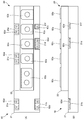
- FIG. 1 is a plan view of the inside of the semiconductor device of the first embodiment
- FIG. 2 is a diagram for explaining the semiconductor device of the first embodiment. Note that FIG. 1 shows a plan view when the case 20 is removed from the semiconductor device 10 of FIG. 2 (A) shows a plan view of the semiconductor device 10, and FIG. 2 (B) shows a side view of the semiconductor device 10 of FIG. 2 (A) from the lower side in the drawing.
- the semiconductor device 10 includes a heat dissipation base plate 30, a plurality of ceramic circuit boards 40a to 40f provided on the heat dissipation base plate 30, and control wiring units 50a to 50f.
- the ceramic circuit boards 40a to 40f are referred to as ceramic circuit boards 40 when they are not distinguished from each other.
- the control wiring units 50a to 50f are referred to as control wiring units 50 when they are not distinguished from each other.
- the semiconductor device 10 is provided with lead frames 60a to 60c for positive electrodes, negative electrodes, and outputs electrically connected to each ceramic circuit board 40, respectively.
- the lead frames 60a to 60c for the positive electrode, the negative electrode, and the output are referred to as lead frames 60 when they are not distinguished from each other.
- a case 20 is mounted on a heat dissipation base plate 30 (see FIG. 2).
- the ceramic circuit board 40 and the control wiring unit 50 on the heat dissipation base plate 30 are covered with a case 20.
- the ceramic circuit boards 40a to 40f are arranged in a row on the front surface of the heat dissipation base plate 30 along the long side of the heat dissipation base plate 30.
- the ceramic circuit board 40 is joined to the front surface of the heat dissipation base plate 30 via, for example, solder or silver wax.
- the ceramic circuit boards 40a to 40f are bonded to the first semiconductor chips 45a and 46a and the second semiconductor chips 45b and 46b, which will be described later, and are electrically connected by bonding wires.
- the bonding wire is made of a material having excellent conductivity.
- the material is composed of, for example, gold, silver, copper, aluminum, or an alloy containing at least one of these.
- the diameter of the bonding wire is, for example, 100 ⁇ m or more and 500 ⁇ m or less.
- the control wiring units 50a, 50c, 50e are located on the heat dissipation base plate 30 and above the ceramic circuit boards 40a, 40c, 40e in FIG.
- the control wiring units 50b, 50d, and 50f are located on the heat dissipation base plate 30 and below the ceramic circuit boards 40a, 40d, and 40e in FIG.
- Such a control wiring unit 50 has an insulating plate 51, a circuit pattern 52 provided on the insulating plate 51, and a control lead frame 60d joined on the circuit pattern 52.
- the control wiring unit 50f is formed with a circuit pattern 52 and a control lead frame 60d. In the other control wiring unit 50, two sets of the circuit pattern 52 and the control lead frame 60d are formed.
- the insulating plate 51 is made of ceramics having good thermal conductivity. Such ceramics are composed of, for example, a composite material containing aluminum oxide and zirconium oxide added to the aluminum oxide as a main component, or a material containing silicon nitride as a main component.
- the thickness of the insulating plate 51 is 0.5 mm or more and 2.0 mm or less.
- the insulating plate 51 has a rectangular shape in a plan view. Further, the corners may be chamfered into an R shape or a C shape.
- the plurality of circuit patterns 52 are made of a metal having excellent conductivity. Such metals are, for example, silver, copper, nickel, or alloys containing at least one of these.
- the thickness of the plurality of circuit patterns 52 is 0.5 mm or more and 1.5 mm or less.
- the surfaces of the plurality of circuit patterns 52 may be plated in order to improve the corrosion resistance. At this time, the plating material used is, for example, nickel, nickel-phosphorus alloy, nickel-boron alloy.
- the plurality of circuit patterns 52 for the insulating plate 51 are obtained by forming a metal plate on the front surface of the insulating plate 51 and performing a treatment such as etching on the metal plate.
- a plurality of circuit patterns 52 cut out from the metal plate in advance may be crimped to the front surface of the insulating plate 51.
- the plurality of circuit patterns 52 shown in FIG. 1 are an example. If necessary, the number, shape, size, etc. of the circuit pattern 52 may be appropriately selected.
- the control lead frame 60d is made of a metal having excellent conductivity. Such metals are, for example, silver, copper, nickel, or alloys containing at least one of these.
- the surface of the control lead frame 60d may be plated to improve corrosion resistance. At this time, the plating material used is, for example, nickel, nickel-phosphorus alloy, nickel-boron alloy.
- a control external connection terminal 62d is provided at the tip of the control lead frame 60d.
- the positive electrode, negative electrode, and output lead frames 60a to 60c may also be made of a metal having excellent conductivity and may be plated. Further, the positive electrode lead frame 60a is connected to two positive electrode external connection terminals 62a. The negative electrode lead frame 60b is connected to two negative electrode external connection terminals 62b. One output external connection terminal 62c is connected to the output lead frame 60c.
- the heat dissipation base plate 30 is made of a metal having excellent thermal conductivity. Such metals are, for example, aluminum, iron, silver, copper, or alloys containing at least one of these.
- the surface of the heat dissipation base plate 30 may be plated in order to improve corrosion resistance. At this time, the plating material used is, for example, nickel, nickel-phosphorus alloy, nickel-boron alloy.
- a cooler (not shown) may be attached to the back surface of the heat dissipation base plate 30 of the semiconductor device 10 via thermal grease. This also makes it possible to improve heat dissipation.
- the thermal grease is, for example, silicone mixed with a metal oxide filler.
- the cooler in this case is made of, for example, aluminum, iron, silver, copper, or an alloy containing at least one of these, which has excellent thermal conductivity.
- fins a heat sink composed of a plurality of fins, a water-cooled cooling device, or the like can be applied.
- the heat dissipation base plate 30 may be integrally configured with such a cooler. In that case, it is composed of aluminum, iron, silver, copper, or an alloy containing at least one of these, which has excellent thermal conductivity.
- a material such as nickel may be formed on the surface of the heat dissipation base plate 30 integrated with the cooler by a plating treatment or the like.
- nickel there are nickel-phosphorus alloys, nickel-boron alloys and the like.
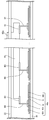
- the case 20 includes a lower storage portion 21 and an upper storage portion 22.
- the lower storage portion 21 has a rectangular shape in a plan view and has a box shape.
- the upper storage portion 22 is also rectangular in a plan view, and has a box shape smaller than that of the lower storage portion 21.
- the lower storage portion 21 and the upper storage portion 22 are integrally connected to each other, and the inside is hollow.
- the ceramic circuit board 40, the positive electrode, the negative electrode, the output, the control lead frames 60a to 60d, and the like are housed in the cavity of the case 20.
- Such a case 20 is made of a thermoplastic resin. Examples of such a resin include polyphenylene sulfide resin, polybutylene terephthalate resin, polybutylene succinate resin, polyamide resin, acrylonitrile butadiene styrene resin and the like.
- Control terminal areas 21a, 21c, 21e recessed on the back surface side of the case 20 are provided on the front surface of the lower storage portion 21 along one long side. From the control terminal areas 21a, 21c, 21e, the control external connection terminals 62d of the control lead frame 60d are represented, respectively. Control terminal areas 21b, 21d, 21f recessed on the back surface side of the case 20 are provided on the front surface of the lower storage portion 21 along the other long side. From the control terminal areas 21b, 21d, 21f, the control external connection terminals 62d of the control lead frame 60d are represented, respectively.
- an output external connection terminal 62c From the front surface of the upper storage portion 22, along the long side, an output external connection terminal 62c, a positive electrode external connection terminal 62a, a negative electrode external connection terminal 62b, a positive electrode external connection terminal 62a, and a negative electrode external connection The terminals 62b and the terminals 62b are respectively exposed.
- the output external connection terminal 62c has a flat plate shape, extends vertically upward from one long side of the front surface of the upper storage portion 22, and is folded back toward the front surface side.
- the positive electrode external connection terminal 62a, the negative electrode external connection terminal 62b, the positive electrode external connection terminal 62a, and the negative electrode external connection terminal 62b are all flat, and are from the other long side of the front surface of the upper storage portion 22. It extends vertically upward and is folded back toward the front surface.
- FIG. 3 is a plan view of a ceramic circuit board included in the semiconductor device of the first embodiment. Although the ceramic circuit board 40a is shown in FIG. 3, other ceramic circuit boards have the same configuration.
- the ceramic circuit board 40a is arranged with the first semiconductor chips 45a and 46a and the second semiconductor chips 45b and 46b, and is electrically connected by a bonding wire (not shown).
- the first semiconductor chips 45a and 46a are switching elements made of silicon or silicon carbide.
- the switching element is, for example, an IGBT or a power MOSFET.
- a collector electrode is provided as a main electrode on the back surface
- a gate electrode is provided as a control electrode
- an emitter electrode is provided as a main electrode on the front surface.
- the second semiconductor chips 45b and 46b are diode elements made of silicon or silicon carbide.
- the diode element is, for example, an FWD (Free Wheeling Diode) such as an SBD (Schottky Barrier Diode) or a PiN (P-intrinsic-N) diode.
- FWD Free Wheeling Diode
- SBD Schottky Barrier Diode
- PiN PiN diode.
- Such second semiconductor chips 45b and 46b are provided with a cathode electrode as a main electrode on the back surface and an anode electrode as a main electrode on the front surface.
- soldering (not shown).
- Lead-free solder is used as the solder.
- the lead-free solder may be, for example, at least one of an alloy consisting of tin-silver-copper, an alloy consisting of tin-zinc-bismuth, an alloy consisting of tin-copper, and an alloy consisting of tin-silver-indium-bismuth. It is the main component.
- the solder may contain additives. Additives are, for example, nickel, germanium, cobalt or silicon.
- the thicknesses of the first semiconductor chips 45a and 46a and the second semiconductor chips 45b and 46b are, for example, 180 ⁇ m or more and 220 ⁇ m or less, and the average is about 200 ⁇ m.
- the ceramic circuit board 40a has an insulating plate 41 and a metal plate 43 (see FIG. 5) formed on the back surface of the insulating plate 41. Further, the ceramic circuit board 40a has circuit patterns 42a to 42e formed on the front surface of the insulating plate 41, respectively. In the following, when the circuit patterns 42a to 42e are not particularly distinguished, they are referred to as circuit patterns 42.
- the insulating plate 41 is the same as the insulating plate 51, and is made of high thermal conductive ceramics such as aluminum oxide, aluminum nitride, and silicon nitride, which have excellent thermal conductivity.
- the metal plate 43 is made of a metal such as aluminum, iron, silver, copper, or an alloy containing at least one of these, which has excellent thermal conductivity.
- the circuit patterns 42a to 42e are the same as the circuit pattern 52, and are made of a metal such as copper or a copper alloy having excellent conductivity. Then, in order to improve the corrosion resistance, for example, a material such as nickel may be formed on the surface by a plating treatment or the like. Specifically, in addition to nickel, there are nickel-phosphorus alloys, nickel-boron alloys and the like. The thickness of the circuit patterns 42a to 42e is, for example, 0.1 mm or more and 1 mm or less.
- a DCB (Direct Copper Bonding) substrate or an AMB (Active Metal Brazing) substrate can be used as the ceramic circuit board 40a having such a configuration.
- the ceramic circuit board 40a can conduct the heat generated by the first and second semiconductor chips 45a and 45b to the heat dissipation base plate 30 via the circuit patterns 42a and 42b, the insulating plate 41 and the metal plate 43.
- the circuit pattern 42a constitutes the collector pattern of the first arm portion A.
- collector electrodes formed on the back surfaces of the first and second semiconductor chips 45a and 45b are joined via solder.
- the circuit pattern 42a has a substantially rectangular shape, and a portion to which the leg portion 64 of the positive electrode lead frame 60a is joined protrudes from the lower side in FIG.
- the circuit pattern 42d constitutes the control pattern of the first arm portion A.
- the bonding wire 47a connected to the gate electrode of the first semiconductor chip 45a is connected.
- the circuit pattern 42d is electrically connected to the control wiring unit 50b by a bonding wire (not shown).
- the circuit pattern 42b constitutes the emitter pattern of the first arm portion A and the collector pattern of the second arm portion B.
- the circuit pattern 42b is connected to a bonding wire 47b connected to an output electrode (emitter electrode) of the first and second semiconductor chips 45a and 45b on the circuit pattern 42a. Further, in the circuit pattern 42b, collector electrodes formed on the back surfaces of the first and second semiconductor chips 46a and 46b are joined via solder.
- the circuit pattern 42b has a substantially rectangular shape, and the upper portion in FIG. 3 is projected.
- the circuit pattern 42b is arranged side by side with the circuit pattern 42a. Further, the circuit pattern 42b is electrically connected to the control wiring unit 50a by a bonding wire (not shown).
- the circuit pattern 42e constitutes the control pattern of the second arm portion B.
- the circuit pattern 42e is connected to the bonding wire 47c connected to the gate electrode of the first semiconductor chip 46a.
- the circuit pattern 42c constitutes the emitter pattern of the second arm portion B.
- the circuit pattern 42c is connected to the bonding wire 47d connected to the output electrode (emitter electrode) of the second semiconductor chip 46b.
- the circuit pattern 42c is arranged on the lower side in FIG. 3 of the circuit pattern 42b. In such a circuit pattern 42c, the leg portion 64 of the negative electrode lead frame 60b is joined.
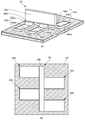
- FIG. 4 is a plan view of a plurality of ceramic circuit boards connected by a lead frame included in the semiconductor device of the first embodiment.
- FIG. 4 is a plan view of a plurality of ceramic circuit boards connected by a lead frame included in the semiconductor device of the first embodiment.
- FIG. 5 is a side view of a plurality of ceramic circuit boards connected by a lead frame included in the semiconductor device of the first embodiment.
- the description of the heat dissipation base plate 30 is omitted.
- FIG. 5 shows the side surface of the positive electrode lead frame 60a only. Further, FIG. 5 shows a part of the upper storage portion 22 of the case 20.
- the positive electrode lead frame 60a includes a main body portion 61, a positive electrode external connection terminal 62a, a linking portion 63, and a leg portion 64.
- the positive electrode lead frame 60a is provided with a leg portion 64 (and a linking portion 63) at a position corresponding to the ceramic circuit board 40 to be connected to the main body portion 61.
- the positive electrode lead frame 60a is provided with a positive electrode external connection terminal 62a with respect to the main body 61 according to the position exposed from the case 20.
- the lead frames 60b and 60c for the negative electrode and the output are also provided with the leg portions 64 (and the linking portion 63) at positions corresponding to the ceramic circuit board 40 to be connected to the main body portion 61.
- the lead frames 60b and 60c for the negative electrode and the output are for the negative electrode, which are not shown in FIGS. 4 and 5, depending on the positions exposed from the case 20 with respect to the main body 61 as shown in FIG. It is provided with external connection terminals 62b and 62c for output.
- the main body 61 has a flat plate shape, and as shown in FIGS. 4 and 5, a plurality of ceramic circuit boards 40 arranged in one direction are extended from the front surface to a predetermined height in the wiring direction. It is provided.
- the positive electrode, negative electrode, and output external connection terminals 62a to 62c are flat plates, project vertically with respect to the front surface of the ceramic circuit board 40, and are integrally connected to the main body 61. ..
- the positive electrode, negative electrode, and output external connection terminals 62a to 62c are provided so as to face the front surface of the upper storage portion 22 of the case 20, respectively.
- the positive electrode, negative electrode, and output external connection terminals 62a to 62c extend vertically from the front surface of the upper storage portion 22 of the case 20.
- the external connection terminals 62a to 62c for the positive electrode, the negative electrode, and the output extending from the front surface of the upper storage portion 22 of the case 20, as shown in FIG. 2, the positive electrode, the negative electrode, and the output
- the main surface of the external connection terminals 62a to 62c is exposed on the front surface of the upper storage portion 22.
- the leg portions 64 are electrically connected to the circuit patterns 42a to 42c of each ceramic circuit board 40 for each of the positive electrode, negative electrode, and output lead frames 60a to 60c. The details of the leg portion 64 will be described later.
- the linking portion 63 is integrally connected to the main body portion 61 and the leg portion 64. Therefore, the linking portion 63 electrically connects the main body portion 61 and the leg portion 64.
- FIG. 6 is a perspective view of a leg portion of a lead frame included in the semiconductor device of the first embodiment. Note that FIG. 6 shows the leg portion 64 (lower end portion side) of the lead frame 60, which is joined to the circuit pattern 42. In the lead frame 60, the main body portion 61 and the linking portion 63 are not shown.
- the leg portion 64 includes a vertical portion 64a and a split portion 64b, 64c.
- the width of the leg portion 64 is uniform in the vertical portion 64a and the divided portions 64b, 64c.
- the thickness of the divided portions 64b and 64c is approximately half the thickness of the vertical portion 64a, respectively. That is, the thickness of the vertical portion 64a is obtained by matching the thicknesses of the divided portions 64b and 64c.
- the vertical portion 64a extends in the vertical direction with respect to the circuit pattern 42.
- the vertical portion 64a is connected to the linking portion 63 at the stretching destination.
- the split portion 64b further includes a continuation portion 64b1 and a parallel portion 64b2.
- the continuation portion 64b1 bends in a predetermined direction from the branch portion 64a1 at the lower end portion of the vertical portion 64a on the circuit pattern 42 side.
- the predetermined direction is the thickness direction.
- the predetermined direction is divided so as to be split from a rift formed so as to cross the other end in parallel with the width direction at the other end of the sandwiched one end (vertical portion 64a) as described later.
- the parallel portion 64b2 is continuously extended from the continuation portion 64b1 in parallel with the circuit pattern 42, and is joined to the circuit pattern 42 by the circuit pattern joining region 64b3 on the back surface.
- the split portion 64c is provided on the opposite side of the split portion 64b and includes a continuation portion 64c1 and a parallel portion 64c2.
- the continuation portion 64c1 bends from the branch portion 64a1 at the lower end portion of the vertical portion 64a on the circuit pattern 42 side to the opposite side in a predetermined direction.
- the parallel portion 64c2 is continuously extended from the continuation portion 64c1 in parallel with the circuit pattern 42, and is joined to the circuit pattern 42 by the circuit pattern joining region 64c3 on the back surface.
- Such a leg portion 64 is attached to the circuit pattern 42 via a linking portion 63 with respect to the main body portion 61 so that a predetermined direction in the divided portions 64b and 64c is parallel to the wiring direction of the main body portion 61. ..
- the length from the branch portion 64a1 of the split portion 64b to the tip portion in the predetermined direction is equal to the length from the branch portion 64a1 of the split portion 64c to the tip portion on the opposite side in the predetermined direction.
- the widths of the divided portions 64b and 64c are the same, the areas of the divided portions 64b and 64c are equal, and in particular, the areas of the parallel portions 64b2 and 64c2 are equal.
- such a leg portion 64 sandwiches and fixes one end portion (vertical portion 64a) of a rectangular and plate-shaped conductive plate, and crosses the width parallel to the other end portion in the width direction.
- Form a rift It is obtained by dividing the crevice so as to be split and bending the divided pieces in opposite directions. Therefore, the thickness of the vertical portion 64a is the total thickness of the divided portions 64b and 64c. At this time, it is desirable that the thickness of the divided portions 64b and 64c is half the thickness of the vertical portions 64a, respectively.
- the divided portions 64b and 64c are joined to the circuit pattern 42. As will be described later, the divided portions 64b and 64c are bonded to the circuit pattern 42 by ultrasonic bonding.
- the leg portion 64 is stably joined to the circuit pattern 42.
- the vertical portion 64a is reliably and stably supported by the split portions 64b and 64c on the front surface side and the back surface side, respectively.
- the continuation portions 64b1 and 64c1 are not joined to the circuit pattern 42, and elasticity is exhibited between the vertical portion 64a and the division portions 64b and 64c. Therefore, the continuation portions 64b1 and 64c1 can alleviate the impact from the outside on the leg portions 64. Therefore, deformation, misalignment, and the like of the vertical portion 64a are prevented, and the lead frame 60 can be maintained at a predetermined joint location.
- FIG. 7 is a flowchart showing a method of manufacturing the semiconductor device according to the first embodiment.
- FIG. 8 is a diagram for explaining an ultrasonic bonding step included in the method for manufacturing a semiconductor device according to the first embodiment.
- Step S10 in FIG. 7 a preparation step of preparing a case 20, a heat dissipation base plate 30, a ceramic circuit board 40, control wiring units 50a to 50e, first semiconductor chips 45a and 46a and second semiconductor chips 45b and 46b, a lead frame 60, and the like is performed ( Step S10 in FIG. 7).
- the lead frame 60 is formed with the leg portion 64 shown in FIG. 6 in advance.
- step S11 in FIG. 7 The ceramic circuit board 40 and the control wiring units 50a to 50e are placed on the front surface of the heat dissipation base plate 30 via solder. Further, the first semiconductor chips 45a and 46a and the second semiconductor chips 45b and 46b are placed on the circuit pattern 42 of the ceramic circuit board 40 via solder, respectively.
- step S11 step S12 in FIG. 7
- it is heated to melt the solder.
- the solder After the solder has melted, it is cooled to solidify the solder, so that the ceramic circuit board 40 and the control wiring units 50a to 50e are joined to the heat dissipation base plate 30 by solder, respectively.
- the first semiconductor chips 45a and 46a and the second semiconductor chips 45b and 46b are joined to the circuit pattern 42 of the ceramic circuit board 40 by soldering, respectively.
- a wiring step is performed in which the ceramic circuit board 40 is electrically connected to the first semiconductor chips 45a, 46a and the second semiconductor chips 45b, 46b by a bonding wire, and wiring is performed (step S13 in FIG. 7). ).
- an ultrasonic bonding step of bonding the leg portion 64 of the lead frame 60 to the circuit pattern 42 of the ceramic circuit board 40 by ultrasonic bonding is performed (step S14 in FIG. 7). Ultrasonic bonding is performed by an ultrasonic bonding device.
- the ultrasonic bonding apparatus includes an ultrasonic generator and an ultrasonic tool 70, which is shown in FIG. 8, for propagating ultrasonic waves generated from the ultrasonic generator.
- the circuit pattern joining regions 64b3 and 64c3 of the parallel portions 64b2 and 64c2 of the leg portions 64 are arranged at the joining portions of the circuit pattern 42.
- Two ultrasonic tools 70 of the ultrasonic bonding device are set in parallel portions 64b2 and 64c2 of the leg portion 64, respectively, as shown in FIG.
- the ultrasonic tool 70 has an L-shape and includes a pressing portion 71 and a propagation portion 72 connected to the pressing portion 71.
- the pressing portion 71 includes a flat surface abutting on the front side of the parallel portions 64b2 and 64c2 of the leg portion 64.
- the propagation portion 72 is provided with a pressing portion 71 on one end side thereof, and the other end side is connected to the ultrasonic wave generator.
- the propagation unit 72 propagates the ultrasonic vibration generated from the ultrasonic wave generator to the pressing unit 71.
- the pressing portion 71 of the ultrasonic tool 70 presses the parallel portions 64b2, 64c2 of the leg portion 64 while simultaneously vibrating against the circuit pattern 42. Then, the parallel portions 64b2 and 64c2 are simultaneously deformed by ultrasonic vibration and parallel to the vibration direction (for example, the bending direction of the divided portions 64b and 64c) (for example, the arrow direction of the broken line in FIG. 8). That is, since the parallel portions 64b2 and 64c2 are similarly deformed along the vibration direction, the parallel portions 64b2 and 64c2 can be joined to the circuit pattern 42 without the vertical portions 64a being displaced.
- the lead frame 60 is appropriately bonded to a predetermined bonding portion of the plurality of ceramic circuit boards 40.
- the parallel portions 64b2 and 64c2 of the leg portions 64 may be pressed and joined by the pressing portion 71 of the ultrasonic tool 70 as follows. That is, in the lead frame 60 provided with the plurality of leg portions 64, the parallel portions 64b2, 64c2 are provided along the main end portion 61 from the leg portion 64 at one end to the leg portion 64 at the other end by the ultrasonic tool 71. It may be alternately ultrasonically bonded to the ceramic circuit substrate 40.
- the parallel portion 64b2 of the leg portion 64 at the end of the positive electrode lead frame 60a is bonded to the ceramic circuit board 40a by ultrasonic bonding, and the parallel portion 64c2 of the leg portion 64 is bonded to the ceramic circuit board 40a by ultrasonic bonding.
- the parallel portion 64b2 of the leg portion 64 adjacent to the leg portion 64 at the end of the positive electrode lead frame 60a is bonded to the ceramic circuit board 40b by ultrasonic bonding
- the parallel portion 64c2 of the leg portion 64 is bonded to the ceramic circuit. It is bonded to the substrate 40b by ultrasonic bonding.
- the leg portions 64 are joined to the ceramic circuit board 40 in the order of parallel portions 64b and 64c2 along the main body portion 61.
- the parallel portion 64b2 of the leg portion 64 at the final end of the positive electrode lead frame 60a is bonded to the ceramic circuit board 40f by ultrasonic bonding, and the parallel portion 64c2 of the leg portion 64 is ultrasonically bonded to the ceramic circuit board 40f. Bond by. It should be noted that not only when the parallel portions 64b2, 64c2 of the plurality of leg portions 64 are alternately joined along the main body portion 61 of the lead frame 60, the parallel portions 64c2, 64b2 of the plurality of leg portions 64 along the main body portion 61 are not limited. May be joined alternately.
- the legs 64 provided on the lead frame 60 are joined in order from the ceramic circuit board 40a toward the ceramic circuit board 40f, as in the case where the parallel portions 64b2 and 64c2 of the legs 64 are joined at the same time.
- the misalignment of the leg portion 64 of the lead frame 60 does not increase as it approaches the ceramic circuit board 40f. Therefore, the lead frame 60 is appropriately bonded to a predetermined bonding portion of the plurality of ceramic circuit boards 40.
- the positive electrode, negative electrode, output, and control external connection terminals 62a to 62d are exposed from each position of the case 20, and the case 20 is attached to the heat dissipation base plate 30 with an adhesive (step S15 in FIG. 7). .. As a result, the semiconductor device 10 shown in FIG. 2 is obtained.
- the semiconductor device 10 is provided on the first semiconductor chips 45a, 46a, the second semiconductor chips 45b, 46b, the insulating plate 41, and the insulating plate 41, and the first semiconductor chips 45a, 46a and the second semiconductor chips 45b, 46b.
- a ceramic circuit board 40 having a circuit pattern 42 electrically connected to and.
- the semiconductor device 10 includes a lead frame 60 having a leg portion 64 to which a circuit pattern 42 is bonded at one end and external connection terminals 62a to 62c for positive electrodes, negative electrodes, and outputs at the other end.
- the leg portion 64 further includes a vertical portion 64a and a split portion 64b, 64c.
- the vertical portion 64a extends in the vertical direction with respect to the circuit pattern 42.
- the split portion 64b is bent in a predetermined direction from the branch portion 64a1 at the lower end of the vertical portion 64a on the circuit pattern 42 side, extends parallel to the circuit pattern 42, and is joined to the circuit pattern 42.
- the divided portion 64c is bent from the branched portion 64a1 in the opposite direction in a predetermined direction, extends in parallel with the circuit pattern 42, and is joined to the circuit pattern 42.
- leg portion 64 In such a leg portion 64, the vertical portion 64a is reliably supported by the front surface side and the back surface side by the divided portions 64b and 64c, respectively. Therefore, the leg portion 64 is stably joined to the circuit pattern 42. Further, since the leg portion 64 is divided in the thickness direction, the divided portions 64b and 64c are thinner than the vertical portion 64a, and the joint portions 64b3 between the parallel portions 64b and 64c and the circuit pattern 42 are formed. Ultrasonic vibration is easily transmitted to 64c3, and it is possible to bond more firmly. Further, such leg portions 64 are simultaneously joined to the circuit pattern 42 by dividing portions 64b and 64c by ultrasonic vibration.
- the semiconductor device 10 can be appropriately manufactured.
- FIG. 9 is a perspective view of a leg portion of a lead frame included in the semiconductor device of the second embodiment. Note that FIG. 9 shows only the leg portion 64. The leg portion 64 of the second embodiment is provided in place of the leg portion 64 of the lead frame 60 of the first embodiment. Therefore, other configurations of the semiconductor device of the second embodiment have the same configuration as that of the semiconductor device 10 of the first embodiment.
- the leg portion 64 shown in FIG. 9 includes a vertical portion 64a and a split portion 64b, 64c.
- the vertical portion 64a extends in the vertical direction with respect to the circuit pattern 42.
- the vertical portion 64a is connected to the linking portion 63 at the stretching destination.
- the divided portions 64b and 64c are cut and divided at one place perpendicular to the vertical portion 64a with respect to the width direction of the vertical portion 64a. Therefore, the combined width of the divided portions 64b and 64c corresponds to the width of the vertical portion 64a.
- the split portion 64b further includes a continuation portion 64b1 and a parallel portion 64b2.
- the continuation portion 64b1 bends in a predetermined direction from the branch portion 64a1 at the lower end portion of the vertical portion 64a on the circuit pattern 42 side, as in the first embodiment.
- the parallel portion 64b2 is continuously extended from the continuation portion 64b1 in parallel with the circuit pattern 42, and is joined to the circuit pattern 42 by the circuit pattern joining region 64b3 on the back surface.
- the split portion 64c is provided on the opposite side of the split portion 64b and includes a continuation portion 64c1 and a parallel portion 64c2.
- the continuation portion 64c1 bends from the branch portion 64a1 at the lower end portion of the vertical portion 64a on the circuit pattern 42 side to the opposite side in a predetermined direction.
- the parallel portion 64c2 is continuously extended from the continuation portion 64c1 in parallel with the circuit pattern 42, and is joined to the circuit pattern 42 by the circuit pattern joining region 64c3 on the back surface. Further, in such a leg portion 64, as in the first embodiment, the parallel portion 64b2, 64c2 of the leg portion 64 is first implemented with respect to the circuit pattern 42 by the pressing portion 71 of the ultrasonic tool 70. It can be joined by pressing while vibrating at the same time or alternately vibrating in the same manner as in the above form.
- Such a leg portion 64 is also attached to the circuit pattern 42 so that a predetermined direction in the divided portions 64b and 64c is parallel to the wiring direction of the main body portion 61 via the linking portion 63 with respect to the main body portion 61.
- the length from the branch portion 64a1 of the split portion 64b to the tip portion in the predetermined direction is equal to the length from the branch portion 64a1 of the split portion 64c to the tip portion on the opposite side in the predetermined direction.
- the divided portions 64b and 64c are divided at the center of the width of the vertical portion 64a, the respective widths are the same, so that the areas of the divided portions 64b and 64c are the same, and in particular, the areas of the parallel portions 64b2 and 64c2. Are equal.
- FIG. 10 is a diagram for explaining another leg of a lead frame included in the semiconductor device of the second embodiment.
- 10 (A) shows a perspective view of the leg portion 64
- FIG. 10 (B) shows a plan view of the leg portion 64.
- the divided portion 64c is not shown, but is arranged on the back side of the vertical portion 64a.
- the leg portion 64 shown in FIG. 10 includes a vertical portion 64a and a divided portion 64b to 64e.
- the vertical portion 64a extends in the vertical direction with respect to the circuit pattern 42.
- the vertical portion 64a is connected to the linking portion 63 at the stretching destination.
- the divided portions 64b to 64e are perpendicular to the vertical portion 64a with respect to the width direction of the vertical portion 64a and are cut and divided at three points at equal intervals. Therefore, the combined width of the divided portions 64b to 64e corresponds to the width of the vertical portion 64a. That is, the leg portion 64 shown in FIG. 10 includes two sets of the divided portions 64b and 64c of the leg portion 64 shown in FIG.
- the leg portion 64 shown in FIG. 10 is not limited to the case where two sets of the leg portions 64 shown in FIG. 9 are included, and may include three or more sets.
- the split portion 64b further includes a continuation portion 64b1 and a parallel portion 64b2.
- the continuation portion 64b1 bends in a predetermined direction from the branch portion 64a1 at the lower end portion of the vertical portion 64a on the circuit pattern 42 side.
- the parallel portion 64b2 is continuously extended from the continuation portion 64b1 in parallel with the circuit pattern 42, and is joined to the circuit pattern 42 by the circuit pattern joining region 64b3 on the back surface.
- the divided portion 64d also includes a continuous portion 64d1 and a parallel portion 64d2.
- the continuation portion 64d1 bends in a predetermined direction from the branch portion 64a1 at the lower end portion of the vertical portion 64a on the circuit pattern 42 side.
- the parallel portion 64d2 is continuously extended from the continuation portion 64d1 in parallel with the circuit pattern 42, and is joined to the circuit pattern 42 by the circuit pattern joining region 64d3 on the back surface.
- the divided portion 64c is provided on the opposite side of the divided portions 64b and 64d of the vertical portion 64a, and includes a continuous portion 64c1 and a parallel portion 64c2 (see FIG. 9).
- the continuation portion 64c1 bends from the branch portion 64a1 at the lower end portion of the vertical portion 64a on the circuit pattern 42 side to the opposite side of the continuation portion 64b1.
- the parallel portion 64c2 is continuously extended from the continuation portion 64c1 in parallel with the circuit pattern 42, and is joined to the circuit pattern 42 by the circuit pattern joining region 64c3 on the back surface.
- the split portion 64e is provided on the opposite side of the split portions 64b and 64d of the vertical portion 64a, and includes a continuation portion 64e1 and a parallel portion 64e2.
- the continuation portion 64e1 bends from the branch portion 64a1 at the lower end portion of the vertical portion 64a on the circuit pattern 42 side to the opposite side in a predetermined direction.
- the parallel portion 64e2 is continuously extended from the continuation portion 64e1 in parallel with the circuit pattern 42, and is joined to the circuit pattern 42 by the circuit pattern joining region 64e3 on the back surface.
- Such a leg portion 64 is also attached to the circuit pattern 42 via a linking portion 63 with respect to the main body portion 61 so that a predetermined direction in the divided portions 64b to 64e is parallel to the wiring direction of the main body portion 61.
- the length from the branch portion 64a1 of the split portion 64b to the tip portion in the predetermined direction, the length from the branch portion 64a1 of the split portion 64c to the tip portion on the opposite side in the predetermined direction, and the branch portion of the split portion 64d is equal to the length from the branch portion 64a1 of the split portion 64e to the tip on the opposite side in the predetermined direction.
- the divided portions 64b to 64e are divided into three at equal intervals with respect to the width of the vertical portion 6a, and since the respective widths are the same, the areas of the divided portions 64b to 64e are the same, and in particular, the parallel portions 64b2 to 64e2. The areas are equal.
- Such a leg portion 64 can also be joined to the circuit pattern 42 by the pressing portion 71 of the ultrasonic tool 70, as in the first embodiment.
- the ultrasonic tool 70 is prepared corresponding to the divided portions 64b to 64e of the leg portion 64, and the divided portions 64b to 64e are joined by simultaneously vibrating and pressing against the circuit pattern 42. Can be done.
- the vertical portion 64a is surely divided into the front surface side and the back surface side by the divided portions 64b and 64c (64b to 64e), respectively. Be supported. Therefore, the leg portion 64 is stably joined to the circuit pattern 42. Further, such leg portions 64 are simultaneously joined to the circuit pattern 42 by dividing portions 64b and 64c (64b to 64e) by ultrasonic vibration. Then, since the divided portions 64b and 64c (64b to 64e) are similarly deformed in parallel with the bending direction, the vertical portion 64a does not shift in position. Therefore, the positional deviation of the vertical portion 64a is prevented, and the lead frame 60 can be maintained at a predetermined joint location. As a result, the semiconductor device can be appropriately manufactured.
Landscapes
- Engineering & Computer Science (AREA)
- Microelectronics & Electronic Packaging (AREA)
- Physics & Mathematics (AREA)
- Power Engineering (AREA)
- Condensed Matter Physics & Semiconductors (AREA)
- General Physics & Mathematics (AREA)
- Computer Hardware Design (AREA)
- Manufacturing & Machinery (AREA)
- Thermal Sciences (AREA)
- Geometry (AREA)
- Lead Frames For Integrated Circuits (AREA)
- Cooling Or The Like Of Semiconductors Or Solid State Devices (AREA)
Abstract
リードフレームの脚部の接合箇所の位置ずれを防止する。 脚部(64)は、垂直部(64a)と分割部(64b,64c)とをさらに備える。垂直部(64a)は、回路パターン(42)に対して鉛直方向に延伸する。分割部(64b)は、垂直部(64a)の回路パターン(42)側の下端部の分岐部(64a1)から所定方向に屈曲し回路パターン(42)に対して平行に延伸して、回路パターン(42)に接合される。分割部(64c)は、分岐部(64a1)から所定方向の反対方向に屈曲し回路パターン(42)に対して平行に延伸して、回路パターン(42)に接合される。このような脚部(64)では、垂直部(64a)がおもて面側、裏面側がそれぞれ分割部(64b,64c)で確実に支持される。
Description
本発明は、半導体装置及び半導体装置の製造方法に関する。
半導体装置は、例えば、IGBT(Insulated Gate Bipolar Transistor)、パワーMOSFET(Metal Oxide Semiconductor Field Effect Transistor)といった半導体素子を含んでいる。半導体装置は、放熱板と、当該放熱板上にそれぞれ接合された、半導体素子が設けられたセラミック回路基板とを備える。さらに、半導体装置では、各セラミック回路基板の回路パターンがリードフレームによりそれぞれ電気的に接続されている。リードフレームは、本体部と本体部に接続された複数の外部接続端子と本体部に接続された複数の脚部とを有する。本体部は複数のセラミック回路基板上を通過するように延伸している。外部接続端子は外部機器等に電気的に接続されている。外部接続端子は、本体部に対して電流を入力または本体部を導通する電流を外部に出力する。脚部は側面視でL字形を成している。このような脚部は、複数のセラミック回路基板上を通過する本体部に沿って、本体部にそれぞれ接続されている。脚部は、各セラミック回路基板の回路パターンに電気的に接合されて、各セラミック回路基板と本体部とを電気的に接続する。この際、脚部は、セラミック回路基板の回路パターンに超音波接合により接合される。このようなリードフレームは、例えば、銅または銅合金により構成されている。
リードフレームの脚部は超音波接合により本体部の回路パターンに接合される。接合される際、脚部は振動方向に応じて接合予定箇所から位置ずれして接合されてしまう場合がある。複数の脚部のうち、本体部の一端部に位置する脚部から本体部の延伸方向に沿って順に脚部の超音波接合を行うと、本体部の一端部の反対側の他端側に連れて、回路パターンに対する脚部の位置ずれが大きくなってしまう。このようにして脚部が接合されたリードフレームはセラミック回路基板に対して寸法公差が大きくなってしまい、半導体装置を製造できなくなってしまう場合がある。
本発明は、このような点に鑑みてなされたものであり、リードフレームの脚部の接合箇所の位置ずれが防止された半導体装置及び半導体装置の製造方法を提供することを目的とする。
本発明の一観点によれば、半導体チップと、絶縁板と前記絶縁板に設けられ、前記半導体チップと電気的に接続される回路パターンとを有する絶縁回路基板と、一端に前記回路パターンが接合される脚部を含み、他端に外部接続端子を備える配線部材と、を備え、前記脚部は、前記回路パターンに対して鉛直方向に延伸する垂直部と、前記垂直部の前記回路パターン側の下端部の分岐部から所定方向に屈曲し前記回路パターンに対して平行に延伸して、前記回路パターンに接合される第1分割部と、前記分岐部から前記所定方向の反対方向に屈曲し前記回路パターンに対して平行に延伸して、前記回路パターンに接合される第2分割部と、を備える、半導体装置が提供される。
また、本発明の一観点によれば、絶縁板と前記絶縁板に設けられた回路パターンとを有する絶縁回路基板と、一端に前記回路パターンに接合される脚部を含み、他端に外部接続端子を備え、前記脚部は、前記回路パターンに対して鉛直方向に延伸する垂直部と、前記垂直部の前記回路パターン側の下端部の分岐部から所定方向に屈曲し前記回路パターンに対して平行に延伸して、前記回路パターンに接合される第1分割部と、前記分岐部から前記所定方向の反対方向に屈曲し前記回路パターンに対して平行に延伸して、前記回路パターンに接合される第2分割部とを備える配線部材と、を用意する用意工程と、前記回路パターンに前記脚部の前記第1分割部及び前記第2分割部を配置して、前記第1分割部及び前記第2分割部を前記回路パターンに超音波接合により同時に接合する超音波接合工程と、を有する半導体装置の製造方法が提供される。
開示の技術によれば、回路パターンに対してリードフレームの脚部の接合箇所の位置ずれが防止され、半導体装置を適切に製造することができる。
本発明の上記及び他の目的、特徴及び利点は本発明の例として好ましい実施の形態を表す添付の図面と関連した以下の説明により明らかになるであろう。
以下、図面を参照して、実施の形態について説明する。なお、以下の説明において、「おもて面」及び「上面」とは、図2の半導体装置10において、上側を向いた面を表す。同様に、「上」とは、図2の半導体装置10において、上側の方向を表す。「裏面」及び「下面」とは、図2の半導体装置10において、下側を向いた面を表す。同様に、「下」とは、図2の半導体装置10において、下側の方向を表す。必要に応じて他の図面でも同様の方向性を意味する。「おもて面」、「上面」、「上」、「裏面」、「下面」、「下」、「側面」は、相対的な位置関係を特定する便宜的な表現に過ぎず、本発明の技術的思想を限定するものではない。例えば、「上」及び「下」は、必ずしも地面に対する鉛直方向を意味しない。つまり、「上」及び「下」の方向は、重力方向に限定されない。
[第1の実施の形態]
第1の実施の形態の半導体装置10について図1及び図2を用いて説明する。図1は、第1の実施の形態の半導体装置の内部の平面図であり、図2は、第1の実施の形態の半導体装置を説明するための図である。なお、図1は、図2の半導体装置10からケース20を取り外したときの平面図を表している。また、図2(A)は、半導体装置10の平面図、図2(B)は図2(A)の半導体装置10を図中下側からの側面図をそれぞれ表している。
第1の実施の形態の半導体装置10について図1及び図2を用いて説明する。図1は、第1の実施の形態の半導体装置の内部の平面図であり、図2は、第1の実施の形態の半導体装置を説明するための図である。なお、図1は、図2の半導体装置10からケース20を取り外したときの平面図を表している。また、図2(A)は、半導体装置10の平面図、図2(B)は図2(A)の半導体装置10を図中下側からの側面図をそれぞれ表している。
半導体装置10は、図1に示されるように、放熱ベース板30と放熱ベース板30上に設けられた複数のセラミック回路基板40a~40f及び制御配線ユニット50a~50fとを含む。なお、セラミック回路基板40a~40fは、それぞれを区別しない場合には、セラミック回路基板40と表す。また、制御配線ユニット50a~50fは、それぞれを区別しない場合には、制御配線ユニット50と表す。そして、半導体装置10は、各セラミック回路基板40に電気的に接続された正極用,負極用,出力用リードフレーム60a~60cがそれぞれ設けられている。なお、正極用,負極用,出力用リードフレーム60a~60cは、それぞれ区別しない場合には、リードフレーム60と表す。このような、半導体装置10は、放熱ベース板30上にケース20が取り付けられている(図2を参照)。放熱ベース板30上のセラミック回路基板40及び制御配線ユニット50はケース20により覆われている。
セラミック回路基板40a~40fは、放熱ベース板30のおもて面に、放熱ベース板30の長辺に沿って一列にそれぞれ配置されている。セラミック回路基板40は、放熱ベース板30のおもて面に対して、例えば、はんだまたは銀ろう等を介して接合されている。セラミック回路基板40a~40fは、後述する第1半導体チップ45a,46a及び第2半導体チップ45b,46bが接合され、ボンディングワイヤにより電気的に接続されている。ボンディングワイヤは、導電性に優れた材質により構成されている。当該材質として、例えば、金、銀、銅、アルミニウム、または、少なくともこれらの一種を含む合金により構成されている。また、ボンディングワイヤの径は、例えば、100μm以上、500μm以下である。なお、セラミック回路基板40並びに第1半導体チップ45a,46a及び第2半導体チップ45b,46bの詳細については後述する。
制御配線ユニット50a,50c,50eは、放熱ベース板30上であって、図1中、セラミック回路基板40a,40c,40eの上方に配置されている。制御配線ユニット50b,50d,50fは、放熱ベース板30上であって、図1中、セラミック回路基板40a,40d,40eの下方に配置されている。このような制御配線ユニット50は、絶縁板51と絶縁板51上に設けられた回路パターン52と回路パターン52上に接合された制御用リードフレーム60dとを有している。なお、制御配線ユニット50のうち、制御配線ユニット50fは、回路パターン52及び制御用リードフレーム60dが一組形成されている。他の制御配線ユニット50は、回路パターン52及び制御用リードフレーム60dが二組形成されている。
絶縁板51は、熱伝導性のよいセラミックスにより構成されている。このようなセラミックスは、例えば、酸化アルミニウムと当該酸化アルミニウムに添加された酸化ジルコニウムとを主成分とする複合材料、または、窒化珪素を主成分とする材料により構成されている。また、絶縁板51の厚さは、0.5mm以上、2.0mm以下である。絶縁板51は、平面視で、矩形状である。また、角部がR形状や、C形状に面取りされていてもよい。
複数の回路パターン52は、導電性に優れた金属により構成されている。このような金属は、例えば、銀、銅、ニッケル、または、少なくともこれらの一種を含む合金である。また、複数の回路パターン52の厚さは、0.5mm以上、1.5mm以下である。複数の回路パターン52の表面に対して、耐食性を向上させるために、めっき処理を行ってもよい。この際、用いられるめっき材は、例えば、ニッケル、ニッケル-リン合金、ニッケル-ボロン合金である。絶縁板51に対する複数の回路パターン52は、絶縁板51のおもて面に金属板を形成し、この金属板に対してエッチング等の処理を行って得られる。または、あらかじめ金属板から切り出した複数の回路パターン52を絶縁板51のおもて面に圧着させてもよい。なお、図1に示す複数の回路パターン52は一例である。必要に応じて、回路パターン52の個数、形状、大きさ等を適宜選択してもよい。
制御用リードフレーム60dは、導電性に優れた金属により構成されている。このような金属は、例えば、銀、銅、ニッケル、または、少なくともこれらの一種を含む合金である。制御用リードフレーム60dの表面に対して、耐食性を向上させるために、めっき処理を行ってもよい。この際、用いられるめっき材は、例えば、ニッケル、ニッケル-リン合金、ニッケル-ボロン合金である。また、制御用リードフレーム60dの先端部には、制御用外部接続端子62dが設けられている。
正極用,負極用,出力用リードフレーム60a~60cもまた、制御用リードフレーム60dと同様に、導電性に優れた金属により構成されて、めっき処理が行われてもよい。また、正極用リードフレーム60aは、二つの正極用外部接続端子62aが接続されている。負極用リードフレーム60bは、二つの負極用外部接続端子62bが接続されている。出力用リードフレーム60cは、一つの出力用外部接続端子62cが接続されている。
放熱ベース板30は、熱伝導性に優れた金属により構成されている。このような金属は、例えば、アルミニウム、鉄、銀、銅、または、少なくともこれらの一種を含む合金である。放熱ベース板30の表面に対して、耐食性を向上させるために、めっき処理を行ってもよい。この際、用いられるめっき材は、例えば、ニッケル、ニッケル-リン合金、ニッケル-ボロン合金である。なお、このような半導体装置10の放熱ベース板30の裏面に冷却器(図示を省略)を、サーマルグリースを介して取りつけてもよい。これにより放熱性を向上させることも可能である。なお、サーマルグリースは、例えば、金属酸化物のフィラーが混入されたシリコーンである。この場合の冷却器は、例えば、熱伝導性に優れたアルミニウム、鉄、銀、銅、または、少なくともこれらの一種を含む合金等により構成されている。また、冷却器として、フィン、または、複数のフィンから構成されるヒートシンク並びに水冷による冷却装置等を適用することができる。また、放熱ベース板30は、このような冷却器と一体的に構成されてもよい。その場合は、熱伝導性に優れたアルミニウム、鉄、銀、銅、または、少なくともこれらの一種を含む合金により構成される。そして、耐食性を向上させるために、例えば、ニッケル等の材料をめっき処理等により冷却器と一体化された放熱ベース板30の表面に形成してもよい。具体的には、ニッケルの他に、ニッケル-リン合金、ニッケル-ボロン合金等がある。
ケース20は、下部収納部21と上部収納部22とを含んでいる。下部収納部21は平面視で矩形状であって、箱型を成している。上部収納部22もまた平面視で矩形状であって、下部収納部21よりも小さい箱型を成している。下部収納部21と上部収納部22とは一体的に接続されており、内部が空洞になっている。ケース20の空洞内に、セラミック回路基板40、正極用,負極用,出力用,制御用リードフレーム60a~60d等が収納される。このようなケース20は、熱可塑性樹脂により構成されている。このような樹脂として、ポリフェニレンサルファイド樹脂、ポリブチレンテレフタレート樹脂、ポリブチレンサクシネート樹脂、ポリアミド樹脂、または、アクリロニトリルブタジエンスチレン樹脂等が挙げられる。
下部収納部21のおもて面に一方の長辺に沿って、ケース20の裏面側に窪んだ制御端子領域21a,21c,21eが設けられている。制御端子領域21a,21c,21eから、制御用リードフレーム60dの制御用外部接続端子62dがそれぞれ表出されている。下部収納部21のおもて面に他方の長辺に沿って、ケース20の裏面側に窪んだ制御端子領域21b,21d,21fが設けられている。制御端子領域21b,21d,21fから、制御用リードフレーム60dの制御用外部接続端子62dがそれぞれ表出されている。上部収納部22のおもて面からは、長辺に沿って、出力用外部接続端子62cと正極用外部接続端子62aと負極用外部接続端子62bと正極用外部接続端子62aと負極用外部接続端子62bとがそれぞれ表出されている。なお、出力用外部接続端子62cは、平板状であって、上部収納部22のおもて面の一方の長辺側から鉛直上方に延出して、おもて面側に折り返されている。正極用外部接続端子62aと負極用外部接続端子62bと正極用外部接続端子62aと負極用外部接続端子62bとも平板状であって、上部収納部22のおもて面の他方の長辺側から鉛直上方に延出して、おもて面側に折り返されている。
次に、セラミック回路基板40について図3を用いて説明する。図3は、第1の実施の形態の半導体装置に含まれるセラミック回路基板の平面図である。なお、図3では、セラミック回路基板40aを示しているものの、他のセラミック回路基板も同様の構成を成している。
セラミック回路基板40aは、第1半導体チップ45a,46a及び第2半導体チップ45b,46bが配置され、図示を省略するボンディングワイヤにより電気的に接続されている。第1半導体チップ45a,46aは、シリコンまたは炭化シリコンにより構成されたスイッチング素子である。スイッチング素子は、例えば、IGBT、パワーMOSFETである。第1半導体チップ45a,46aがIGBTである場合には、裏面に主電極としてコレクタ電極を、おもて面に、制御電極としてゲート電極及び主電極としてエミッタ電極をそれぞれ備えている。第1半導体チップ45a,46aがパワーMOSFETである場合には、裏面に主電極としてドレイン電極を、おもて面に、制御電極としてゲート電極及び主電極としてソース電極をそれぞれ備えている。また、第2半導体チップ45b,46bは、シリコンまたは炭化シリコンにより構成されたダイオード素子である。ダイオード素子は、例えば、SBD(Schottky Barrier Diode)、PiN(P-intrinsic-N)ダイオード等のFWD(Free Wheeling Diode)である。このような第2半導体チップ45b,46bは、裏面に主電極としてカソード電極を、おもて面に主電極としてアノード電極をそれぞれ備えている。第1半導体チップ45a,46a及び第2半導体チップ45b,46bは、その裏面側が所定の回路パターン42a,42b上にはんだ(図示を省略)により接合されている。はんだは、鉛フリーはんだが用いられる。鉛フリーはんだは、例えば、錫-銀-銅からなる合金、錫-亜鉛-ビスマスからなる合金、錫-銅からなる合金、錫-銀-インジウム-ビスマスからなる合金のうち少なくともいずれかの合金を主成分とする。さらに、はんだには、添加物が含まれてもよい。添加物は、例えば、ニッケル、ゲルマニウム、コバルトまたはシリコンである。はんだは、添加物が含まれることで、濡れ性、光沢、結合強度が向上し、信頼性の向上を図ることができる。はんだに代わり、金属焼結体を用いてもよい。また、第1半導体チップ45a,46a及び第2半導体チップ45b,46bの厚さは、例えば、180μm以上、220μm以下であって、平均は、200μm程度である。
セラミック回路基板40aは、絶縁板41と絶縁板41の裏面に形成された金属板43(図5を参照)とを有している。さらに、セラミック回路基板40aは、絶縁板41のおもて面に形成された回路パターン42a~42eをそれぞれ有している。なお、以下では、回路パターン42a~42eを特に区別しない場合には、回路パターン42と表す。絶縁板41は、絶縁板51と同様であって、熱伝導性に優れた、酸化アルミニウム、窒化アルミニウム、窒化珪素等の高熱伝導性のセラミックスにより構成されている。金属板43は、熱伝導性に優れたアルミニウム、鉄、銀、銅、または、少なくともこれらの一種を含む合金等の金属により構成されている。回路パターン42a~42eは、回路パターン52と同様であって、導電性に優れた銅あるいは銅合金等の金属により構成されている。そして、耐食性を向上させるために、例えば、ニッケル等の材料をめっき処理等により表面に形成してもよい。具体的には、ニッケルの他に、ニッケル-リン合金、ニッケル-ボロン合金等がある。また、回路パターン42a~42eの厚さは、例えば、0.1mm以上、1mm以下である。このような構成を有するセラミック回路基板40aとして、例えば、DCB(Direct Copper Bonding)基板、AMB(Active Metal Brazed)基板を用いることができる。セラミック回路基板40aは、第1,第2半導体チップ45a,45bで発生した熱を回路パターン42a,42b、絶縁板41及び金属板43を介して、放熱ベース板30に伝導させることができる。
回路パターン42aは、第1アーム部Aのコレクタパターンを構成する。回路パターン42aは、第1,第2半導体チップ45a,45bの裏面に形成されたコレクタ電極がはんだを介して接合されている。回路パターン42aは、略矩形状を成しており、図3中下側に正極用リードフレーム60aの脚部64が接合される部分が突出している。回路パターン42dは、第1アーム部Aの制御パターンを構成する。回路パターン42dは、第1半導体チップ45aのゲート電極と接続されたボンディングワイヤ47aが接続される。さらに、回路パターン42dは、制御配線ユニット50bとボンディングワイヤ(図示を省略)により電気的に接続される。
回路パターン42bは、第1アーム部Aのエミッタパターン及び第2アーム部Bのコレクタパターンを構成する。回路パターン42bは、回路パターン42a上の第1,第2半導体チップ45a,45bの出力電極(エミッタ電極)と接続されたボンディングワイヤ47bが接続されている。また、回路パターン42bは、第1,第2半導体チップ46a,46bの裏面に形成されたコレクタ電極がはんだを介して接合されている。回路パターン42bは、略矩形状を成しており、図3中上側の部分が突出している。回路パターン42bは、回路パターン42aと並んで、配置される。さらに、回路パターン42bは、制御配線ユニット50aとボンディングワイヤ(図示を省略)により電気的に接続される。回路パターン42eは、第2アーム部Bの制御パターンを構成する。回路パターン42eは、第1半導体チップ46aのゲート電極と接続されたボンディングワイヤ47cが接続されている。
回路パターン42cは、第2アーム部Bのエミッタパターンを構成する。回路パターン42cは、第2半導体チップ46bの出力電極(エミッタ電極)と接続されたボンディングワイヤ47dが接続されている。回路パターン42cは、回路パターン42bの図3中下側に配置されている。このような回路パターン42cは、負極用リードフレーム60bの脚部64が接合される。
半導体装置10では、このような第1半導体チップ45a,46a及び第2半導体チップ45b,46bが接合されたセラミック回路基板40が放熱ベース板30のおもて面に放熱ベース板30の長手方向に沿って複数配置されている。さらに、複数のセラミック回路基板40に適宜電気的に接続される正極用,負極用,出力用リードフレーム60a~60cが設けられている。このような、複数のセラミック回路基板40及び正極用,負極用,出力用リードフレーム60a~60cについて、図4及び図5を用いて説明する。図4は、第1の実施の形態の半導体装置に含まれるリードフレームで接続された複数のセラミック回路基板の平面図である。図5は、第1の実施の形態の半導体装置に含まれるリードフレームで接続された複数のセラミック回路基板の側面図である。なお、図4では、放熱ベース板30の記載は省略している。図5は、正極用リードフレーム60aのみの側面を示している。また、図5では、ケース20のうち上部収納部22の一部を示している。
図4及び図5に示されるように、一方向に配置されたセラミック回路基板40a~40fに対して、正極用,負極用,出力用リードフレーム60a~60cが適宜電気的に接合されている。正極用リードフレーム60aは、本体部61と正極用外部接続端子62aと連係部63と脚部64とを含んでいる。正極用リードフレーム60aは、本体部61に対して、接続されるセラミック回路基板40に応じた位置に脚部64(並びに連係部63)を備えている。正極用リードフレーム60aは、本体部61に対して、ケース20から表出する位置に応じて、正極用外部接続端子62aを備えている。また、負極用,出力用リードフレーム60b,60cもまた、本体部61に対して、接続されるセラミック回路基板40に応じた位置に脚部64(並びに連係部63)を備えている。負極用,出力用リードフレーム60b,60cは、本体部61に対して、図2で示したようにケース20から表出する位置に応じて、図4及び図5で図示を省略する負極用,出力用外部接続端子62b,62cを備えている。
本体部61は、平板状であって、図4及び図5に示されるように、一方向に複数配置されたセラミック回路基板40のおもて面から所定の高さにおいて配線方向に延伸して設けられている。正極用,負極用,出力用外部接続端子62a~62cは、平板状であって、セラミック回路基板40のおもて面に対して鉛直方向に突出して本体部61に一体的に接続されている。なお、正極用,負極用,出力用外部接続端子62a~62cは、それぞれ、ケース20の上部収納部22のおもて面に対向するように設けられている。ケース20が放熱ベース板30に取り付けられると、正極用,負極用,出力用外部接続端子62a~62cがケース20の上部収納部22のおもて面から鉛直方向に延出する。ケース20の上部収納部22のおもて面から延出する正極用,負極用,出力用外部接続端子62a~62cを折り曲げることで、図2に示されるように、正極用,負極用,出力用外部接続端子62a~62cの主面が上部収納部22のおもて面に表出される。
脚部64は、正極用,負極用,出力用リードフレーム60a~60cごとに、各セラミック回路基板40の回路パターン42a~42cに接合されて電気的に接続されている。なお、脚部64の詳細については後述する。連係部63は、本体部61と脚部64とに一体的に接続されている。よって、連係部63は本体部61と脚部64とを電気的に接続する。
次に、正極用,負極用,出力用リードフレーム60a~60cの脚部64の詳細について、図6を用いて説明する。図6は、第1の実施の形態の半導体装置に含まれるリードフレームの脚部の斜視図である。なお、図6では、回路パターン42に接合されている、リードフレーム60の脚部64(の下端部側)を示している。リードフレーム60において本体部61及び連係部63の図示を省略している。
脚部64は、垂直部64aと分割部64b,64cとを含んでいる。脚部64の幅は、垂直部64a及び分割部64b,64cにおいて均一である。なお、後述するように、分割部64b,64cの厚さは、それぞれ、垂直部64aの厚さの略半分であることが望ましい。すなわち、分割部64b,64cの厚さを合わせることで垂直部64aの厚さとなる。垂直部64aは、回路パターン42に対して鉛直方向に延伸する。垂直部64aは延伸先で連係部63と接続される。分割部64bは、さらに、継続部64b1と平行部64b2とを備える。継続部64b1は、垂直部64aの回路パターン42側の下端部の分岐部64a1から所定方向に屈曲する。所定方向とは、厚さ方向である。または、所定方向とは、後述するように挟持された一端部(垂直部64a)に対する他端部に幅方向に対して平行に他端部を横切るように形成された裂け目から割くように分割する方向である。平行部64b2は、継続部64b1から継続して回路パターン42に対して平行に延伸して、裏面の回路パターン接合領域64b3により回路パターン42に接合されている。他方、分割部64cは、分割部64bの反対側に設けられ、継続部64c1と平行部64c2とを備える。継続部64c1は、垂直部64aの回路パターン42側の下端部の分岐部64a1から所定方向の反対側に屈曲する。平行部64c2は、継続部64c1から継続して回路パターン42に対して平行に延伸して、裏面の回路パターン接合領域64c3により回路パターン42に接合されている。
このような脚部64は、本体部61に対して連係部63を介して、分割部64b,64cにおける所定方向が本体部61の配線方向に平行になるように回路パターン42に取り付けられている。脚部64において、分割部64bの分岐部64a1から所定方向の先端部までの長さと、分割部64cの分岐部64a1から所定方向の反対側の先端部までの長さとが等しい。また、分割部64b,64cの幅は等しいため、分割部64b,64cの面積は等しく、特に、平行部64b2,64c2の面積が等しい。
また、このような脚部64は、矩形状であって板状の導電板の一端部(垂直部64a)を挟持して固定し、他端部に幅方向に対して平行に当該幅を横切る裂け目を形成する。当該裂け目から割くように分割し、分割したものをそれぞれ反対方向に屈曲させて得られる。このため、垂直部64aの厚さは、分割部64b,64cを合わせた厚さである。なお、この際、分割部64b,64cの厚さは、それぞれ、垂直部64aの厚さの半分であることが望ましい。このようにして得られた脚部64では、分割部64b,64cが回路パターン42に接合される。後述するように、分割部64b,64cは、回路パターン42に超音波接合で接合されている。このため、分割部64b,64cと回路パターン42との間には、接合部材がなく、直接接合されている。したがって、脚部64は、回路パターン42に対して安定して接合されるようになる。また、垂直部64aはおもて面側、裏面側がそれぞれ分割部64b,64cで確実にかつ安定して支持される。さらに、継続部64b1,64c1は回路パターン42に接合されておらず、垂直部64aと分割部64b,64cとの間で弾性を発現する。このため、継続部64b1,64c1は脚部64に対する外部からの衝撃を緩和することができる。したがって、垂直部64aの変形、位置ずれ等が防止され、リードフレーム60を所定の接合箇所に維持することができる。
次に、このように回路パターン42に接合された脚部64を含む半導体装置10の製造方法について、図7及び図8を用いて説明する。図7は、第1の実施の形態の半導体装置の製造方法を示すフローチャートである。図8は、第1の実施の形態の半導体装置の製造方法に含まれる超音波接合工程を説明するための図である。
まず、ケース20、放熱ベース板30、セラミック回路基板40、制御配線ユニット50a~50e、第1半導体チップ45a,46a及び第2半導体チップ45b,46b、リードフレーム60等を用意する用意工程を行う(図7のステップS10)。この際、リードフレーム60は、予め、図6に示した脚部64が形成されている。
次いで、以下の載置工程を行う(図7のステップS11)。放熱ベース板30のおもて面の所定箇所に、セラミック回路基板40、制御配線ユニット50a~50eをはんだを介してそれぞれ載置する。さらに、セラミック回路基板40の回路パターン42に第1半導体チップ45a,46a及び第2半導体チップ45b,46bをはんだを介してそれぞれ載置する。
次いで、ステップS11の状態で以下のはんだ接合工程を行う(図7のステップS12)。まず、加熱してはんだを溶融させる。はんだが溶融した後、冷却してはんだを固化することで、放熱ベース板30に、セラミック回路基板40、制御配線ユニット50a~50eをそれぞれはんだにより接合する。そして、セラミック回路基板40の回路パターン42に第1半導体チップ45a,46a及び第2半導体チップ45b,46bをそれぞれはんだにより接合する。
次いで、ボンディングワイヤにより、セラミック回路基板40と第1半導体チップ45a,46a及び第2半導体チップ45b,46bとの間を電気的に接続して、配線を行う配線工程を行う(図7のステップS13)。次いで、リードフレーム60の脚部64をセラミック回路基板40の回路パターン42に超音波接合により接合する超音波接合工程を行う(図7のステップS14)。超音波接合は超音波接合装置により行われる。超音波接合装置は、超音波発生装置と超音波発生装置から発生された超音波を伝搬させる、図8に示される、超音波ツール70とを含む。まず、脚部64の平行部64b2,64c2の回路パターン接合領域64b3,64c3を回路パターン42の接合箇所に配置する。超音波接合装置の2つの超音波ツール70を、図8に示されるように、脚部64の平行部64b2,64c2にそれぞれセットする。超音波ツール70は、L字状を成しており、押圧部71と押圧部71に接続された伝搬部72とを含む。押圧部71は、脚部64の平行部64b2,64c2のおもて側に当接される平面を含んでいる。伝搬部72は、その一端側に押圧部71を備え、他端側が超音波発生装置に接続されている。伝搬部72は、超音波発生装置から発生された超音波振動を押圧部71に伝搬する。
このような超音波ツール70の押圧部71により、脚部64の平行部64b2,64c2を回路パターン42に対して同時に振動させながら押圧する。すると、平行部64b2,64c2は超音波振動により同時かつ振動方向(例えば、分割部64b,64cの屈曲方向)に対して平行に変形してしまう(例えば、図8中の破線の矢印方向)。すなわち、平行部64b2,64c2が同様に振動方向に沿って変形するために、垂直部64aが位置ずれすることなく、平行部64b2,64c2を回路パターン42に接合することができる。このようにして、リードフレーム60に設けられている各脚部64をセラミック回路基板40aからセラミック回路基板40fに向けて順に接合しても、リードフレーム60の脚部64はセラミック回路基板40fに近づくに連れて位置ずれが大きくなることはない。したがって、リードフレーム60を複数のセラミック回路基板40の所定の接合箇所に対して適切に接合される。
また、超音波ツール70の押圧部71によって脚部64の平行部64b2,64c2を次のように押圧して接合してもよい。すなわち、複数の脚部64が設けられたリードフレーム60において、本端部61に沿って一端部の脚部64から他端部の脚部64まで、超音波ツール71により平行部64b2,64c2を交互にセラミック回路基板40に対して超音波接合してもよい。
例えば、正極用リードフレーム60aの場合について説明する(図4及び図5を参照)。まず、正極用リードフレーム60aの最端部の脚部64の平行部64b2をセラミック回路基板40aに超音波接合により接合し、当該脚部64の平行部64c2をセラミック回路基板40aに超音波接合により接合する。次いで、正極用リードフレーム60aの当該最端部の脚部64の隣の脚部64の平行部64b2をセラミック回路基板40bに超音波接合により接合し、当該脚部64の平行部64c2をセラミック回路基板40bに超音波接合により接合する。このように正極用リードフレーム60aにおいて本体部61に沿って脚部64をセラミック回路基板40に対して平行部64b,64c2の順に接合していく。最終的に、正極用リードフレーム60aの最終端の脚部64の平行部64b2をセラミック回路基板40fに超音波接合により接合し、当該脚部64の平行部64c2をセラミック回路基板40fに超音波接合により接合する。なお、リードフレーム60の本体部61に沿って複数の脚部64の平行部64b2,64c2を交互に接合する場合に限らず、本体部61に沿って複数の脚部64の平行部64c2,64b2を交互に接合してもよい。これらの場合でも、脚部64の平行部64b2,64c2を同時に接合した場合と同様に、リードフレーム60に設けられている各脚部64をセラミック回路基板40aからセラミック回路基板40fに向けて順に接合しても、リードフレーム60の脚部64はセラミック回路基板40fに近づくに連れて位置ずれが大きくなることはない。したがって、リードフレーム60を複数のセラミック回路基板40の所定の接合箇所に対して適切に接合される。
次いで、ケース20の各箇所から正極用,負極用,出力用,制御用外部接続端子62a~62dを表出させて、ケース20を放熱ベース板30に接着剤により取り付ける(図7のステップS15)。以上により、図2に示した半導体装置10が得られる。
上記の半導体装置10は、第1半導体チップ45a,46a及び第2半導体チップ45b,46bと、絶縁板41と絶縁板41に設けられ、第1半導体チップ45a,46a及び第2半導体チップ45b,46bと電気的に接続される回路パターン42とを有するセラミック回路基板40と、を含む。さらに、半導体装置10は、一端に回路パターン42が接合される脚部64を含み、他端に正極用,負極用,出力用外部接続端子62a~62cを備えるリードフレーム60を含む。この際、脚部64は、垂直部64aと分割部64b,64cとをさらに備える。垂直部64aは、回路パターン42に対して鉛直方向に延伸する。分割部64bは、垂直部64aの回路パターン42側の下端部の分岐部64a1から所定方向に屈曲し回路パターン42に対して平行に延伸して、回路パターン42に接合される。分割部64cは、分岐部64a1から所定方向の反対方向に屈曲し回路パターン42に対して平行に延伸して、回路パターン42に接合される。
このような脚部64では、垂直部64aがおもて面側、裏面側がそれぞれ分割部64b,64cで確実に支持される。このため、脚部64は回路パターン42に対して安定して接合されるようになる。また、このような脚部64は厚さ方向に分割されているのでそれぞれの分割部64b,64cが垂直部64aより薄くなっており、平行部64b,64cと回路パターン42との接合部64b3,64c3に超音波振動が伝わり易く、より強固に接合することができる。また、このような脚部64を回路パターン42に対して、分割部64b,64cを超音波振動により同時に接合する。すると、分割部64b,64cが屈曲方向に対して平行に同様に変形するため、垂直部64aが位置ずれすることがない。したがって、垂直部64aの位置ずれ等が防止され、リードフレーム60を所定の接合箇所に維持することができる。この結果、半導体装置10を適切に製造することができる。
[第2の実施の形態]
第2の実施の形態では、第1の実施の形態とは異なる脚部について、図9を用いて説明する。図9は、第2の実施の形態の半導体装置に含まれるリードフレームの脚部の斜視図である。なお、図9は、脚部64のみを示している。第2の実施の形態の脚部64は、第1の実施の形態のリードフレーム60の脚部64に代わって設けられるものである。したがって、第2の実施の形態の半導体装置のその他の構成は、第1の実施の形態の半導体装置10と同様の構成を成している。
第2の実施の形態では、第1の実施の形態とは異なる脚部について、図9を用いて説明する。図9は、第2の実施の形態の半導体装置に含まれるリードフレームの脚部の斜視図である。なお、図9は、脚部64のみを示している。第2の実施の形態の脚部64は、第1の実施の形態のリードフレーム60の脚部64に代わって設けられるものである。したがって、第2の実施の形態の半導体装置のその他の構成は、第1の実施の形態の半導体装置10と同様の構成を成している。
図9に示される脚部64は、垂直部64aと分割部64b,64cとを含んでいる。垂直部64aは、回路パターン42に対して鉛直方向に延伸する。垂直部64aは延伸先で連係部63と接続される。分割部64b,64cは、第1の実施の形態と異なり、垂直部64aの幅方向に対して、垂直部64aに垂直に1か所で切断されて分割されている。したがって、分割部64b,64cを合わせた幅は、垂直部64aの幅に相当する。分割部64bは、さらに、継続部64b1と平行部64b2とを備える。継続部64b1は、垂直部64aの回路パターン42側の下端部の分岐部64a1から、第1の実施の形態と同様に、所定方向に屈曲する。平行部64b2は、継続部64b1から継続して回路パターン42に対して平行に延伸して、裏面の回路パターン接合領域64b3により回路パターン42に接合されている。他方、分割部64cは、分割部64bの反対側に設けられ、継続部64c1と平行部64c2とを備える。継続部64c1は、垂直部64aの回路パターン42側の下端部の分岐部64a1から所定方向の反対側に屈曲する。平行部64c2は、継続部64c1から継続して回路パターン42に対して平行に延伸して、裏面の回路パターン接合領域64c3により回路パターン42に接合されている。また、このような脚部64も、第1の実施の形態と同様に、超音波ツール70の押圧部71により、脚部64の平行部64b2,64c2を回路パターン42に対して第1の実施の形態と同様に同時に振動させながら、または、交互に振動させながら押圧することで接合することができる。
このような脚部64もまた、本体部61に対して連係部63を介して、分割部64b,64cにおける所定方向が本体部61の配線方向に平行になるように回路パターン42に取り付けられている。脚部64において、分割部64bの分岐部64a1から所定方向の先端部までの長さと、分割部64cの分岐部64a1から所定方向の反対側の先端部までの長さとが等しい。また、分割部64b,64cは垂直部64aの幅の中央で分割されている場合には、それぞれの幅が等しいため、分割部64b,64cの面積は等しく、特に、平行部64b2,64c2の面積が等しい。
また、第2の実施の形態の別の脚部について、図10を用いて説明する。図10は、第2の実施の形態の半導体装置に含まれるリードフレームの別の脚部を説明するための図である。なお、図10(A)は、脚部64の斜視図を、図10(B)は、脚部64の平面図をそれぞれ示している。図10(A)では、分割部64cは図示されていないものの、垂直部64aの裏側に配置されている。
図10に示される脚部64は、垂直部64aと分割部64b~64eとを含んでいる。垂直部64aは、回路パターン42に対して鉛直方向に延伸する。垂直部64aは延伸先で連係部63と接続される。分割部64b~64eは、第1の実施の形態と異なり、垂直部64aの幅方向に対して、垂直部64aに垂直であって等間隔に3か所で切断されて分割されている。したがって、分割部64b~64eを合わせた幅は、垂直部64aの幅に相当する。すなわち、図10に示される脚部64は、図9に示した脚部64の分割部64b,64cを二組含んでいる。なお、図10に示される脚部64は、図9に示した脚部64を二組含んでいる場合に限らず、三組以上含んでもよい。
分割部64bは、さらに、継続部64b1と平行部64b2とを備える。継続部64b1は、垂直部64aの回路パターン42側の下端部の分岐部64a1から所定方向に屈曲する。平行部64b2は、継続部64b1から継続して回路パターン42に対して平行に延伸して、裏面の回路パターン接合領域64b3により回路パターン42に接合されている。また、分割部64dもまた、さらに、継続部64d1と平行部64d2とを備える。継続部64d1は、垂直部64aの回路パターン42側の下端部の分岐部64a1から所定方向に屈曲する。平行部64d2は、継続部64d1から継続して回路パターン42に対して平行に延伸して、裏面の回路パターン接合領域64d3により回路パターン42に接合されている。
他方、分割部64cは、垂直部64aの分割部64b,64dの反対側に設けられ、継続部64c1と平行部64c2とを備える(図9を参照)。継続部64c1は、垂直部64aの回路パターン42側の下端部の分岐部64a1から継続部64b1の反対側に屈曲する。平行部64c2は、継続部64c1から継続して回路パターン42に対して平行に延伸して、裏面の回路パターン接合領域64c3により回路パターン42に接合されている。また、分割部64eは、垂直部64aの分割部64b,64dの反対側に設けられ、継続部64e1と平行部64e2とを備える。継続部64e1は、垂直部64aの回路パターン42側の下端部の分岐部64a1から所定方向の反対側に屈曲する。平行部64e2は、継続部64e1から継続して回路パターン42に対して平行に延伸して、裏面の回路パターン接合領域64e3により回路パターン42に接合されている。
このような脚部64もまた、本体部61に対して連係部63を介して、分割部64b~64eにおける所定方向が本体部61の配線方向に平行になるように回路パターン42に取り付けられている。脚部64において、分割部64bの分岐部64a1から所定方向の先端部までの長さと、分割部64cの分岐部64a1から所定方向の反対側の先端部までの長さと、分割部64dの分岐部64a1から所定方向の反対側の先端部までの長さと、分割部64eの分岐部64a1から所定方向の反対側の先端部までの長さとが等しい。また、分割部64b~64eは垂直部6aの幅に対して等間隔に3分割されており、それぞれの幅が等しいため、分割部64b~64eの面積は等しく、特に、平行部64b2~64e2の面積が等しい。
このような脚部64も、第1の実施の形態と同様に、回路パターン42に対して超音波ツール70の押圧部71により接合することができる。但し、この場合は、超音波ツール70を脚部64の分割部64b~64eに対応して用意し、分割部64b~64eを回路パターン42に対して同時に振動させながら押圧することで接合することができる。
このような第2の実施の形態の脚部64でも、第1の実施の形態と同様に、垂直部64aはおもて面側、裏面側がそれぞれ分割部64b,64c(64b~64e)で確実に支持される。このため、脚部64は回路パターン42に対して安定して接合されるようになる。また、このような脚部64を回路パターン42に対して、分割部64b,64c(64b~64e)を超音波振動により同時に接合する。すると、分割部64b,64c(64b~64e)が屈曲方向に対して平行に同様に変形するため、垂直部64aが位置ずれすることがない。したがって、垂直部64aの位置ずれ等が防止され、リードフレーム60を所定の接合箇所に維持することができる。この結果、半導体装置を適切に製造することができる。
上記については単に本発明の原理を示すものである。さらに、多数の変形、変更が当業者にとって可能であり、本発明は上記に示し、説明した正確な構成及び応用例に限定されるものではなく、対応するすべての変形例及び均等物は、添付の請求項及びその均等物による本発明の範囲とみなされる。
10 半導体装置
20 ケース
21 下部収納部
21a,21b,21c,21d,21e,21f 制御端子領域
22 上部収納部
30 放熱ベース板
40,40a~40f セラミック回路基板
41,51 絶縁板
42,42a~42e,52 回路パターン
43 金属板
45a,46a 第1半導体チップ
45b,46b 第2半導体チップ
47a~47d ボンディングワイヤ
50,50a~50f 制御配線ユニット
60 リードフレーム
60a 正極用リードフレーム
60b 負極用リードフレーム
60c 出力用リードフレーム
60d 制御用リードフレーム
61 本体部
62a 正極用外部接続端子
62b 負極用外部接続端子
62c 出力用外部接続端子
62d 制御用外部接続端子
63 連係部
64 脚部
64a 垂直部
64a1 分岐部
64b~64e 分割部
64b1,64c1,64d1,64e1 継続部
64b2,64c2,64d2,64e2 平行部
64b3,64c3,64d3,64e3 回路パターン接合領域
70 超音波ツール
71 押圧部
72 伝搬部
Claims (14)
- 半導体チップと、
絶縁板と前記絶縁板に設けられ、前記半導体チップと電気的に接続される回路パターンとを有する絶縁回路基板と、
一端に前記回路パターンが接合される脚部を含み、他端に外部接続端子を備える配線部材と、
を備え、
前記脚部は、前記回路パターンに対して鉛直方向に延伸する垂直部と、前記垂直部の前記回路パターン側の下端部の分岐部から所定方向に屈曲し前記回路パターンに対して平行に延伸して、前記回路パターンに接合される第1分割部と、前記分岐部から前記所定方向の反対方向に屈曲し前記回路パターンに対して平行に延伸して、前記回路パターンに接合される第2分割部と、を備える、
半導体装置。 - 前記脚部は、板状であって、前記第1分割部及び前記第2分割部は厚さ方向において互いに反対側にそれぞれ分割されている、
請求項1に記載の半導体装置。 - 前記第1分割部の第1厚さと前記第2分割部の第2厚さとは、前記垂直部の第3厚さから2分割されている、
請求項2に記載の半導体装置。 - 前記第1分割部の第1幅と前記第2分割部の第2幅とは、前記垂直部の第3幅から2分割されている、
請求項2に記載の半導体装置。 - 前記脚部は、一組の前記第1分割部及び前記第2分割部が複数組分割されている、
請求項4に記載の半導体装置。 - 平面視における前記第1分割部の第1面積と前記第2分割部の第2面積とは等しい、
請求項4または5に記載の半導体装置。 - 前記分岐部から前記第1分割部の前記所定方向の第1先端部までの長さと、前記分岐部から前記第2分割部の前記所定方向の反対方向の第2先端部までの長さとが同一である、
請求項1乃至6のいずれかに記載の半導体装置。 - 前記配線部材は、前記脚部を複数含み、さらに、前記脚部の前記下端部の反対側の上端部がそれぞれ接続される本体部を備える、
請求項1乃至7のいずれかに記載の半導体装置。 - 前記本体部は、さらに、所定の配線方向に延伸し、前記脚部が前記配線方向に沿って並んで配置されている、
請求項8に記載の半導体装置。 - 前記脚部は、前記本体部に対して、前記所定方向が前記配線方向に平行を成してそれぞれ接続されている、
請求項9に記載の半導体装置。 - 放熱板をさらに備え、
前記放熱板上に、前記絶縁回路基板が前記配線方向に複数配置され、
前記配線部材は、前記本体部が前記絶縁回路基板を跨って前記配線方向に延伸され、前記脚部が前記絶縁回路基板にそれぞれ接合されて、配置されている、
請求項9または10に記載の半導体装置。 - 絶縁板と前記絶縁板に設けられた回路パターンとを有する絶縁回路基板と、
一端に前記回路パターンに接合される脚部を含み、他端に外部接続端子を備え、前記脚部は、前記回路パターンに対して鉛直方向に延伸する垂直部と、前記垂直部の前記回路パターン側の下端部の分岐部から所定方向に屈曲し前記回路パターンに対して平行に延伸して、前記回路パターンに接合される第1分割部と、前記分岐部から前記所定方向の反対方向に屈曲し前記回路パターンに対して平行に延伸して、前記回路パターンに接合される第2分割部とを備える配線部材と、を用意する用意工程と、
前記回路パターンに前記脚部の前記第1分割部及び前記第2分割部を配置して、前記第1分割部及び前記第2分割部を前記回路パターンに超音波接合により同時に接合する超音波接合工程と、
を有する半導体装置の製造方法。 - 前記配線部材は複数の前記脚部を備えており、複数の前記絶縁回路基板の前記回路パターンに対して前記脚部をそれぞれ接合する、
請求項12に記載の半導体装置の製造方法。 - 絶縁板と前記絶縁板に設けられた回路パターンとをそれぞれ有し、一方向に配列された複数の絶縁回路基板と、
一端に、前記複数の絶縁回路基板にそれぞれ対応し、前記回路パターンに接合される複数の脚部を含み、他端に外部接続端子を備え、前記複数の脚部は、前記回路パターンに対して鉛直方向に延伸する垂直部と、前記垂直部の前記回路パターン側の下端部の分岐部から所定方向に屈曲し前記回路パターンに対して平行に延伸して、前記回路パターンに接合される第1分割部と、前記分岐部から前記所定方向の反対方向に屈曲し前記回路パターンに対して平行に延伸して、前記回路パターンに接合される第2分割部とをそれぞれ備える配線部材と、を用意する用意工程と、
前記回路パターンに前記複数の脚部の前記第1分割部及び前記第2分割部をそれぞれ配置して、前記一方向に沿って、前記複数の脚部ごとに前記第1分割部を前記回路パターンに超音波接合により接合し、前記第2分割部を前記回路パターンに前記超音波接合により接合する超音波接合工程と、
を有する半導体装置の製造方法。
Priority Applications (4)
| Application Number | Priority Date | Filing Date | Title |
|---|---|---|---|
| JP2022534946A JP7428254B2 (ja) | 2020-07-09 | 2021-05-28 | 半導体装置及び半導体装置の製造方法 |
| DE112021000211.2T DE112021000211T5 (de) | 2020-07-09 | 2021-05-28 | Halbleitervorrichtung Und Verfahren Zum Herstellen Derselben |
| CN202180007987.8A CN114902389A (zh) | 2020-07-09 | 2021-05-28 | 半导体装置以及半导体装置的制造方法 |
| US17/855,162 US20220330429A1 (en) | 2020-07-09 | 2022-06-30 | Semiconductor device and method of manufacturing the same |
Applications Claiming Priority (2)
| Application Number | Priority Date | Filing Date | Title |
|---|---|---|---|
| JP2020118648 | 2020-07-09 | ||
| JP2020-118648 | 2020-07-09 |
Related Child Applications (1)
| Application Number | Title | Priority Date | Filing Date |
|---|---|---|---|
| US17/855,162 Continuation US20220330429A1 (en) | 2020-07-09 | 2022-06-30 | Semiconductor device and method of manufacturing the same |
Publications (1)
| Publication Number | Publication Date |
|---|---|
| WO2022009556A1 true WO2022009556A1 (ja) | 2022-01-13 |
Family
ID=79552333
Family Applications (1)
| Application Number | Title | Priority Date | Filing Date |
|---|---|---|---|
| PCT/JP2021/020530 WO2022009556A1 (ja) | 2020-07-09 | 2021-05-28 | 半導体装置及び半導体装置の製造方法 |
Country Status (5)
| Country | Link |
|---|---|
| US (1) | US20220330429A1 (ja) |
| JP (1) | JP7428254B2 (ja) |
| CN (1) | CN114902389A (ja) |
| DE (1) | DE112021000211T5 (ja) |
| WO (1) | WO2022009556A1 (ja) |
Citations (2)
| Publication number | Priority date | Publication date | Assignee | Title |
|---|---|---|---|---|
| WO2016031020A1 (ja) * | 2014-08-28 | 2016-03-03 | 三菱電機株式会社 | 半導体装置 |
| WO2019230292A1 (ja) * | 2018-06-01 | 2019-12-05 | 富士電機株式会社 | 半導体装置 |
-
2021
- 2021-05-28 WO PCT/JP2021/020530 patent/WO2022009556A1/ja active Application Filing
- 2021-05-28 CN CN202180007987.8A patent/CN114902389A/zh active Pending
- 2021-05-28 JP JP2022534946A patent/JP7428254B2/ja active Active
- 2021-05-28 DE DE112021000211.2T patent/DE112021000211T5/de active Pending
-
2022
- 2022-06-30 US US17/855,162 patent/US20220330429A1/en active Pending
Patent Citations (2)
| Publication number | Priority date | Publication date | Assignee | Title |
|---|---|---|---|---|
| WO2016031020A1 (ja) * | 2014-08-28 | 2016-03-03 | 三菱電機株式会社 | 半導体装置 |
| WO2019230292A1 (ja) * | 2018-06-01 | 2019-12-05 | 富士電機株式会社 | 半導体装置 |
Also Published As
| Publication number | Publication date |
|---|---|
| JPWO2022009556A1 (ja) | 2022-01-13 |
| DE112021000211T5 (de) | 2022-08-18 |
| CN114902389A (zh) | 2022-08-12 |
| US20220330429A1 (en) | 2022-10-13 |
| JP7428254B2 (ja) | 2024-02-06 |
Similar Documents
| Publication | Publication Date | Title |
|---|---|---|
| US8698289B2 (en) | Semiconductor device, a method of manufacturing the same and an electronic device | |
| JP4438489B2 (ja) | 半導体装置 | |
| CN107615464B (zh) | 电力用半导体装置的制造方法以及电力用半导体装置 | |
| US11088042B2 (en) | Semiconductor device and production method therefor | |
| KR20120127535A (ko) | 프레스 피트 단자 및 반도체 장치 | |
| CN110610920A (zh) | 半导体装置、引线框架以及半导体装置的制造方法 | |
| US9076782B2 (en) | Semiconductor device and method of manufacturing same | |
| WO2013065464A1 (ja) | 半導体装置 | |
| JP7201106B2 (ja) | 半導体装置 | |
| JP2020136449A (ja) | 半導体装置の製造方法 | |
| JP2009141288A (ja) | 電力用半導体モジュール | |
| WO2022009556A1 (ja) | 半導体装置及び半導体装置の製造方法 | |
| JP6380561B2 (ja) | 半導体モジュール | |
| JP4586508B2 (ja) | 半導体装置およびその製造方法 | |
| JP2021090030A (ja) | 半導体装置及び半導体装置の製造方法 | |
| JP7031185B2 (ja) | ウェッジツール及びウェッジボンディング方法 | |
| JP7476540B2 (ja) | 半導体装置 | |
| JP7459465B2 (ja) | 半導体装置及び半導体装置の製造方法 | |
| JP2019083292A (ja) | 半導体装置 | |
| JP4797492B2 (ja) | 半導体装置 | |
| CN113224022A (zh) | 半导体模块和半导体模块的制造方法 | |
| JPWO2022009556A5 (ja) | ||
| JP2021044452A (ja) | 半導体装置 | |
| WO2022137811A1 (ja) | 半導体ユニット及び半導体装置 | |
| WO2020166283A1 (ja) | 半導体装置 |
Legal Events
| Date | Code | Title | Description |
|---|---|---|---|
| 121 | Ep: the epo has been informed by wipo that ep was designated in this application |
Ref document number: 21838264 Country of ref document: EP Kind code of ref document: A1 |
|
| ENP | Entry into the national phase |
Ref document number: 2022534946 Country of ref document: JP Kind code of ref document: A |
|
| 122 | Ep: pct application non-entry in european phase |
Ref document number: 21838264 Country of ref document: EP Kind code of ref document: A1 |