WO2022004807A1 - 半導体装置 - Google Patents
半導体装置 Download PDFInfo
- Publication number
- WO2022004807A1 WO2022004807A1 PCT/JP2021/024812 JP2021024812W WO2022004807A1 WO 2022004807 A1 WO2022004807 A1 WO 2022004807A1 JP 2021024812 W JP2021024812 W JP 2021024812W WO 2022004807 A1 WO2022004807 A1 WO 2022004807A1
- Authority
- WO
- WIPO (PCT)
- Prior art keywords
- layer
- cell region
- region
- sense
- channel
- Prior art date
- Legal status (The legal status is an assumption and is not a legal conclusion. Google has not performed a legal analysis and makes no representation as to the accuracy of the status listed.)
- Ceased
Links
Images


Classifications
-
- H—ELECTRICITY
- H10—SEMICONDUCTOR DEVICES; ELECTRIC SOLID-STATE DEVICES NOT OTHERWISE PROVIDED FOR
- H10D—INORGANIC ELECTRIC SEMICONDUCTOR DEVICES
- H10D30/00—Field-effect transistors [FET]
- H10D30/60—Insulated-gate field-effect transistors [IGFET]
- H10D30/64—Double-diffused metal-oxide semiconductor [DMOS] FETs
- H10D30/66—Vertical DMOS [VDMOS] FETs
- H10D30/669—Vertical DMOS [VDMOS] FETs having voltage-sensing or current-sensing structures, e.g. emulator sections or overcurrent sensing cells
-
- H—ELECTRICITY
- H10—SEMICONDUCTOR DEVICES; ELECTRIC SOLID-STATE DEVICES NOT OTHERWISE PROVIDED FOR
- H10D—INORGANIC ELECTRIC SEMICONDUCTOR DEVICES
- H10D12/00—Bipolar devices controlled by the field effect, e.g. insulated-gate bipolar transistors [IGBT]
- H10D12/01—Manufacture or treatment
- H10D12/031—Manufacture or treatment of IGBTs
- H10D12/032—Manufacture or treatment of IGBTs of vertical IGBTs
- H10D12/038—Manufacture or treatment of IGBTs of vertical IGBTs having a recessed gate, e.g. trench-gate IGBTs
-
- H—ELECTRICITY
- H10—SEMICONDUCTOR DEVICES; ELECTRIC SOLID-STATE DEVICES NOT OTHERWISE PROVIDED FOR
- H10D—INORGANIC ELECTRIC SEMICONDUCTOR DEVICES
- H10D12/00—Bipolar devices controlled by the field effect, e.g. insulated-gate bipolar transistors [IGBT]
- H10D12/411—Insulated-gate bipolar transistors [IGBT]
- H10D12/441—Vertical IGBTs
- H10D12/461—Vertical IGBTs having non-planar surfaces, e.g. having trenches, recesses or pillars in the surfaces of the emitter, base or collector regions
- H10D12/481—Vertical IGBTs having non-planar surfaces, e.g. having trenches, recesses or pillars in the surfaces of the emitter, base or collector regions having gate structures on slanted surfaces, on vertical surfaces, or in grooves, e.g. trench gate IGBTs
-
- H—ELECTRICITY
- H10—SEMICONDUCTOR DEVICES; ELECTRIC SOLID-STATE DEVICES NOT OTHERWISE PROVIDED FOR
- H10D—INORGANIC ELECTRIC SEMICONDUCTOR DEVICES
- H10D30/00—Field-effect transistors [FET]
- H10D30/01—Manufacture or treatment
- H10D30/021—Manufacture or treatment of FETs having insulated gates [IGFET]
- H10D30/028—Manufacture or treatment of FETs having insulated gates [IGFET] of double-diffused metal oxide semiconductor [DMOS] FETs
- H10D30/0291—Manufacture or treatment of FETs having insulated gates [IGFET] of double-diffused metal oxide semiconductor [DMOS] FETs of vertical DMOS [VDMOS] FETs
- H10D30/0297—Manufacture or treatment of FETs having insulated gates [IGFET] of double-diffused metal oxide semiconductor [DMOS] FETs of vertical DMOS [VDMOS] FETs using recessing of the gate electrodes, e.g. to form trench gate electrodes
-
- H—ELECTRICITY
- H10—SEMICONDUCTOR DEVICES; ELECTRIC SOLID-STATE DEVICES NOT OTHERWISE PROVIDED FOR
- H10D—INORGANIC ELECTRIC SEMICONDUCTOR DEVICES
- H10D30/00—Field-effect transistors [FET]
- H10D30/60—Insulated-gate field-effect transistors [IGFET]
- H10D30/64—Double-diffused metal-oxide semiconductor [DMOS] FETs
- H10D30/66—Vertical DMOS [VDMOS] FETs
- H10D30/668—Vertical DMOS [VDMOS] FETs having trench gate electrodes, e.g. UMOS transistors
-
- H—ELECTRICITY
- H10—SEMICONDUCTOR DEVICES; ELECTRIC SOLID-STATE DEVICES NOT OTHERWISE PROVIDED FOR
- H10D—INORGANIC ELECTRIC SEMICONDUCTOR DEVICES
- H10D62/00—Semiconductor bodies, or regions thereof, of devices having potential barriers
- H10D62/10—Shapes, relative sizes or dispositions of the regions of the semiconductor bodies; Shapes of the semiconductor bodies
- H10D62/102—Constructional design considerations for preventing surface leakage or controlling electric field concentration
- H10D62/103—Constructional design considerations for preventing surface leakage or controlling electric field concentration for increasing or controlling the breakdown voltage of reverse-biased devices
- H10D62/105—Constructional design considerations for preventing surface leakage or controlling electric field concentration for increasing or controlling the breakdown voltage of reverse-biased devices by having particular doping profiles, shapes or arrangements of PN junctions; by having supplementary regions, e.g. junction termination extension [JTE]
- H10D62/106—Constructional design considerations for preventing surface leakage or controlling electric field concentration for increasing or controlling the breakdown voltage of reverse-biased devices by having particular doping profiles, shapes or arrangements of PN junctions; by having supplementary regions, e.g. junction termination extension [JTE] having supplementary regions doped oppositely to or in rectifying contact with regions of the semiconductor bodies, e.g. guard rings with PN or Schottky junctions
- H10D62/107—Buried supplementary regions, e.g. buried guard rings
-
- H—ELECTRICITY
- H10—SEMICONDUCTOR DEVICES; ELECTRIC SOLID-STATE DEVICES NOT OTHERWISE PROVIDED FOR
- H10D—INORGANIC ELECTRIC SEMICONDUCTOR DEVICES
- H10D62/00—Semiconductor bodies, or regions thereof, of devices having potential barriers
- H10D62/10—Shapes, relative sizes or dispositions of the regions of the semiconductor bodies; Shapes of the semiconductor bodies
- H10D62/124—Shapes, relative sizes or dispositions of the regions of semiconductor bodies or of junctions between the regions
- H10D62/126—Top-view geometrical layouts of the regions or the junctions
- H10D62/127—Top-view geometrical layouts of the regions or the junctions of cellular field-effect devices, e.g. multicellular DMOS transistors or IGBTs
-
- H—ELECTRICITY
- H10—SEMICONDUCTOR DEVICES; ELECTRIC SOLID-STATE DEVICES NOT OTHERWISE PROVIDED FOR
- H10D—INORGANIC ELECTRIC SEMICONDUCTOR DEVICES
- H10D62/00—Semiconductor bodies, or regions thereof, of devices having potential barriers
- H10D62/10—Shapes, relative sizes or dispositions of the regions of the semiconductor bodies; Shapes of the semiconductor bodies
- H10D62/13—Semiconductor regions connected to electrodes carrying current to be rectified, amplified or switched, e.g. source or drain regions
- H10D62/149—Source or drain regions of field-effect devices
- H10D62/151—Source or drain regions of field-effect devices of IGFETs
- H10D62/156—Drain regions of DMOS transistors
- H10D62/157—Impurity concentrations or distributions
-
- H—ELECTRICITY
- H10—SEMICONDUCTOR DEVICES; ELECTRIC SOLID-STATE DEVICES NOT OTHERWISE PROVIDED FOR
- H10D—INORGANIC ELECTRIC SEMICONDUCTOR DEVICES
- H10D62/00—Semiconductor bodies, or regions thereof, of devices having potential barriers
- H10D62/10—Shapes, relative sizes or dispositions of the regions of the semiconductor bodies; Shapes of the semiconductor bodies
- H10D62/17—Semiconductor regions connected to electrodes not carrying current to be rectified, amplified or switched, e.g. channel regions
- H10D62/213—Channel regions of field-effect devices
-
- H—ELECTRICITY
- H10—SEMICONDUCTOR DEVICES; ELECTRIC SOLID-STATE DEVICES NOT OTHERWISE PROVIDED FOR
- H10D—INORGANIC ELECTRIC SEMICONDUCTOR DEVICES
- H10D62/00—Semiconductor bodies, or regions thereof, of devices having potential barriers
- H10D62/60—Impurity distributions or concentrations
-
- H—ELECTRICITY
- H10—SEMICONDUCTOR DEVICES; ELECTRIC SOLID-STATE DEVICES NOT OTHERWISE PROVIDED FOR
- H10D—INORGANIC ELECTRIC SEMICONDUCTOR DEVICES
- H10D64/00—Electrodes of devices having potential barriers
- H10D64/20—Electrodes characterised by their shapes, relative sizes or dispositions
- H10D64/27—Electrodes not carrying the current to be rectified, amplified, oscillated or switched, e.g. gates
- H10D64/311—Gate electrodes for field-effect devices
- H10D64/411—Gate electrodes for field-effect devices for FETs
- H10D64/511—Gate electrodes for field-effect devices for FETs for IGFETs
- H10D64/512—Disposition of the gate electrodes, e.g. buried gates
- H10D64/513—Disposition of the gate electrodes, e.g. buried gates within recesses in the substrate, e.g. trench gates, groove gates or buried gates
-
- H—ELECTRICITY
- H10—SEMICONDUCTOR DEVICES; ELECTRIC SOLID-STATE DEVICES NOT OTHERWISE PROVIDED FOR
- H10D—INORGANIC ELECTRIC SEMICONDUCTOR DEVICES
- H10D64/00—Electrodes of devices having potential barriers
- H10D64/111—Field plates
- H10D64/117—Recessed field plates, e.g. trench field plates or buried field plates
Definitions
- the present disclosure relates to a semiconductor device provided with a vertical semiconductor switching element having the same structure in a main cell region and a sense cell region, and detects a current flowing in the main cell region based on the current flowing in the sense cell region.
- Patent Document 1 discloses a semiconductor device in which a vertical semiconductor switching element having the same structure is provided in a main cell region and a sense cell region, and a current flowing in the main cell region is detected based on the current flowing in the sense cell region. ..
- This semiconductor device has a planar type gate electrode and has a structure in which a current detection element is arranged as a sense cell region between main elements formed in the main cell region, and has a high resistance between the main element and the sense element. By providing a region, they are electrically separated from each other. With such a structure, the passage of the carrier is matched, and the accuracy of the detection current flowing through the current detection element is improved.
- a vertical semiconductor switching element having the same structure is formed in a main cell region and a sense cell region, and the semiconductor switching element is a first conductive type drift layer and a drift.
- a second conductive type channel layer formed on the layer, a first conductive type first impurity region formed on the surface layer portion of the channel layer in the channel layer and having a higher impurity concentration than the drift layer, and a first.
- a gate insulating film that covers the channel layer between the impurity region and the drift layer, and a plurality of lines arranged in a striped manner with one direction as the longitudinal direction are arranged in a stripe shape and formed on the surface of the gate insulating film.
- a first or second conductive type second impurity formed on the side opposite to the channel layer with the drift layer sandwiched between the gate electrode layer forming the channel region with respect to the channel layer and having a higher impurity concentration than the drift layer. It is configured to have a region, an upper electrode electrically connected to the first impurity region and the channel layer, and a lower electrode electrically connected to the second impurity region.
- the sense cell region is defined as a rectangular region surrounding the operating region of the semiconductor switching element formed as a sense cell, and the dimension in the same direction as the one direction in the main cell region is defined as the lateral dimension and the lateral dimension.
- the dimension in the vertical direction is defined as the vertical dimension, and the vertical dimension is defined as greater than or equal to the horizontal dimension.
- the dimensions are designed so that the vertical dimension of the main cell area is equal to or greater than the horizontal dimension.
- the main current flowing in the main cell region is detected based on the ratio of the sense current flowing in the sense cell region (hereinafter referred to as the sense ratio) to the main current flowing in the main cell region. Therefore, if the amount of change in the sense ratio with respect to the change in the gate voltage is large, the sense ratio can be detected with high sensitivity and accuracy. Therefore, when considering a circuit that detects the sense ratio or sense current of a semiconductor device that drives a vertical semiconductor switching element in a feedback circuit, it is possible to improve the degree of freedom in circuit design in which the gate voltage is controlled by the gate driver circuit. Therefore, it is possible to design the gate voltage dependence.
- the semiconductor switching element includes a first conductive type drift layer, a second conductive type channel layer formed on the drift layer, and the channel layer in the channel layer.
- a first conductive type first impurity region formed on the surface layer and having a higher impurity concentration than the drift layer, and a gate insulating film covering the channel layer between the first impurity region and the drift layer, longitudinally oriented in one direction.
- a gate electrode layer that forms a channel region with respect to the channel layer by being arranged in a stripe shape by arranging a plurality of conductors in the direction and being formed on the surface of the gate insulating film, and a channel layer sandwiching a drift layer.
- a first or second conductive type second impurity region formed on the opposite side and having a higher impurity concentration than the drift layer, an upper electrode electrically connected to the first impurity region and the channel layer, and a second.
- a lower electrode electrically connected to an impurity region is provided, and a resistance component layer having a higher resistance than the drift layer in the main cell region is formed in the drift layer in the sense cell region.
- the drift layer in the sense cell region is provided with a resistance component layer. According to such a configuration, it is possible to reduce the sense current flowing in the sense cell region. Therefore, it is possible to make the gate voltage dependence of the sense cell region and the main cell region substantially the same. Therefore, it is possible to design the gate voltage dependence.
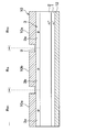
- FIG. 2 is a sectional view taken along line II-II of FIG.
- FIG. 3 is a sectional view taken along line III-III of FIG.
- FIG. 6 is a sectional view taken along line IV-IV of FIG.
- It is a top layout drawing explaining the sense cell area. It is a block diagram which showed the state of driving a semiconductor device by a gate driver circuit. It is a figure which showed the relationship of the sense ratio with respect to the gate voltage. It is a top layout drawing explaining the sense cell region in the semiconductor device which concerns on the modification of 1st Embodiment.
- the first embodiment will be described.
- a semiconductor device provided with an n-channel type vertical MOSFET as a vertical semiconductor switching element having the same structure in the main cell region and the sense cell region will be described.
- the structure of the semiconductor device according to the present embodiment will be described with reference to FIGS. 1 to 4.
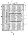
- the semiconductor device is configured to have a main cell region Rm and a sense cell region Rs.
- the main cell region Rm is formed in a rectangular shape with a part cut off, and the sense cell region Rs is arranged in the main cell region Rm and is formed so as to be surrounded by the main cell region Rm.
- FIG. 1 shows only the vicinity of the sense cell region Rs in the main cell region Rm, the main cell region Rm actually has a sufficiently wider area than the sense cell region Rs, for example, an area of 100 million times. Has been done.
- An n-channel type vertical MOSFET having the same structure is formed in the main cell region Rm and the sense cell region Rs.
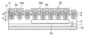
- the semiconductor device is formed by using an n + type semiconductor substrate 1 made of a semiconductor material such as silicon having a high impurity concentration.
- the semiconductor substrate 1 has a thickness of 10 to 300 ⁇ m and an n-type impurity concentration of about 1 ⁇ 10 12 to 1 ⁇ 10 18 cm -3 .
- n + -type impurity concentration than the semiconductor substrate 1 is a low density - type drift layer 2 is formed, n - the desired type drift layer 2
- a channel p-type layer 3 having a relatively low impurity concentration is formed at the position.
- the n - type drift layer 2 has, for example, a thickness of 1 to 10 ⁇ m and an n-type impurity concentration of about 1 ⁇ 10 12 to 1 ⁇ 10 18 cm -3 .
- the thickness of the channel p-type layer 3 is 0 to 2 ⁇ m, and the concentration of p-type impurities is about 1 ⁇ 10 12 to 1 ⁇ 10 18 cm -3 .
- the channel p-type layer 3 is formed by ion-implanting a p-type impurity into the n-type drift layer 2.
- the main channel layer 3a formed in the main cell region Rm and the sense channel layer 3b formed in the sense cell region Rs are continuously connected. It is said to be a structure.
- the surface layer portion of the channel p-type layer 3 is an n + -type impurity region 4 which is a region constituting the source region and corresponds to a first impurity region having a higher impurity concentration than the n-type drift layer 2. Is provided.
- the n + type impurity region 4 has, for example, a thickness of 0 to 2 ⁇ m and an n-type impurity concentration of about 1 ⁇ 10 12 to 1 ⁇ 10 18 cm -3 .
- a trench 5 is formed from the surface side of the substrate , penetrating the n + type impurity region 4 and the channel p type layer 3 and reaching the n ⁇ type drift layer 2.
- a gate insulating film 6 is formed so as to cover the inner wall surface of the trench 5, and a shield electrode 7 and a gate electrode layer 8 composed of doped Poly—Si are formed in the trench 5 via the gate insulating film 6. It is laminated to form a two-layer structure.
- the shield electrode 7 is formed to reduce the capacitance between the gate and the drain and improve the electrical characteristics of the MOSFET by being fixed to the source potential.
- the gate electrode layer 8 performs a MOSFET switching operation, and forms a channel in the channel p-type layer 3 on the side surface of the trench 5 when a gate voltage is applied.
- the trench gate structure is composed of the trench 5, the gate insulating film 6, the shield electrode 7, the gate electrode layer 8 and the insulating film 9.
- This trench gate structure has a striped layout in which, for example, a plurality of lines are arranged in the vertical direction of the paper surface in FIG. 2 as the longitudinal direction, or in the vertical direction of the paper surface in FIG. 2, or in the left-right direction of the paper surface in FIG.
- the formation pitch of the trench gate structure is arbitrary, but is set to, for example, 1 to 2 ⁇ m.
- n + type impurity region 4 is not formed, so that the vertical MOSFET is not formed. ..
- the trench 5 is in a state of being continuously connected by the main cell region Rm and the sense cell region Rs.
- the shield electrode 7 and the gate electrode layer 8 embedded in the trench 5 are also continuously connected to both the main cell region Rm and the sense cell region Rs.
- the shield electrode 7 is outside the main cell region Rm with respect to the gate electrode layer 8, that is, the sense cell region of the main cell region Rm. It extends to the side away from Rs. Then, the portion is exposed as a shield liner from the surface of the channel p-type layer 3, so that an electrical connection with the upper electrode 10 which is a source potential described later can be achieved.
- the gate electrode layer 8 extends beyond the shield electrode 7 to the outside of the main cell region Rm, that is, to the side of the main cell region Rm away from the sense region. There is. The portion is exposed from the surface of the channel p-type layer 3 as a gate liner, and is electrically connected to a gate electrode (not shown).
- an interlayer insulating film 13 composed of an oxide film or the like is formed so as to cover the gate electrode layer 8, and an upper electrode 10 corresponding to a source electrode and a gate electrode (not shown) are formed on the interlayer insulating film 13.
- the upper electrode 10 is electrically connected to the n + type impurity region 4 and the channel p-type layer 3 through a portion where the interlayer insulating film 13 is not formed, for example, a contact hole.
- the gate electrode is also electrically connected to the gate electrode layer 8 via a gate liner through a portion where the interlayer insulating film 13 is not formed, for example, a contact hole.
- the upper electrode 10 is divided into a main electrode 10a formed in the main cell region Rm and a sense electrode 10b formed in the sense cell region Rs, and these are separated by a predetermined distance.
- the main electrode 10a is formed over almost the entire area of the main cell region Rm, and is formed in a rectangular shape with a part cut out.
- the sense electrode 10b has a rectangular shape and is arranged so as to be surrounded by the main electrode 10a.
- the lead-out wiring 10c is drawn out from one side of the sense electrode 10b corresponding to the notched portion of the main cell region Rm to the outside of the main cell region Rm.
- a lower electrode 12 corresponding to a drain electrode is formed on the surface of the n + type semiconductor substrate 1 opposite to the n ⁇ type drift layer 2.
- the semiconductor device having the vertical MOSFET is configured.
- a gate voltage is applied to the gate electrode layer 8 of the vertical MOSFET provided in the main cell region Rm and the sense cell region Rs, a channel is generated on the surface of the channel p-type layer 3 in contact with the trench 5. It is formed.
- the electrons injected from the upper electrode 10 pass through the channel formed in the channel p-type layer 3 from the n + type impurity region 4 and then reach the n ⁇ type drift layer 2, and the upper electrode 10 and the lower electrode The operation of passing a current between the 12 and the 12 is performed.
- a vertical MOSFET having the same cell structure is formed in each of the main cell region Rm and the sense cell region Rs, and the cell area of the vertical MOSFET provided in the main cell region Rm and the sense cell region Rs, in other words, the number of cells is set to a predetermined ratio. It is set to. Therefore, the sense current obtained by reducing the main current flowing in the main cell region Rm by a predetermined ratio can be passed through the sense cell region Rs. Therefore, by outputting the sense current flowing in the sense cell region Rs to the outside, the sense current flowing in the main cell region Rm can be detected.
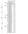
- the vertical direction is defined as the horizontal direction in the sense cell region Rs in the same direction as the longitudinal direction of the trench gate structure and the longitudinal direction in the direction perpendicular to the longitudinal direction. It defines the dimensional relationship between dimensions and lateral dimensions.
- the sense cell region Rs is a rectangular portion that is an operating region of the vertical MOSFET formed as a sense cell. That is, in the sense cell region Rs, the n + type impurity region 4 constituting the source region is formed along the trench gate structure, so that the MOS operation is performed when the gate voltage is applied to the gate electrode layer 8 and the current is generated. It is an area where the current flows.
- the sense cell region Rs is shown as a region that collectively surrounds a plurality of n + type impurity regions 4 that are brought into contact with the sense electrode 10b.
- the vertical dimension of the sense cell region Rs is set to be equal to or larger than the horizontal dimension, in other words, the ratio of the vertical dimension to the horizontal dimension of the sense cell region Rs is set to 1 or more. More preferably, the dimension of the portion serving as the current path (hereinafter referred to as the current path dimension) excluding the width of the trench gate structure from the vertical dimension of the sense cell region Rs is set to be equal to or larger than the horizontal dimension.
- the main current flowing in the main cell region Rm is detected based on the sense ratio. Specifically, as shown in FIG. 6, a gate voltage is applied from the gate driver circuit 100 to the semiconductor device 101 provided with the main cell region Rm and the sense cell region Rs, and the sense ratio or sense current at that time is gated. It feeds back to the driver circuit 100.
- the gate driver circuit 100 includes a feedback circuit, and the sense ratio or sense current is detected by the feedback circuit, and the gate voltage output by the gate driver circuit 100 is adjusted so that the desired main current is obtained. Control.
- FIG. 7 shows the dependence of the sense ratio on the gate voltage (Vgs) (hereinafter referred to as Vgs dependence).
- Vgs dependence the gate voltage
- the sense ratio has a Vgs dependence.
- the horizontal dimension is larger than the vertical dimension of the sense cell region Rs
- the change in the sense ratio with respect to the gate voltage of the element is small.
- the characteristic is that the sense ratio becomes smaller as the gate voltage becomes larger, the sense ratio becomes almost constant regardless of the magnitude of the gate voltage.
- the vertical dimension of the sense cell region Rs is larger than the horizontal dimension as in the present embodiment
- the change in the sense ratio with respect to the gate voltage of the element is large, and the larger the gate voltage is, the larger the sense ratio is. Becomes smaller.
- the larger the gate voltage the larger the rate of decrease in the sense ratio.
- the gate voltage dependence of the entire system including the resistance is suppressed by having the gate voltage dependence of the sense cell itself.
- the sense ratio can be detected with high sensitivity.
- the sense ratio or sense current is fed back to the gate driver circuit 100, but the sense ratio when the gate voltage is set to a predetermined value is fed back to adjust the gate voltage output by the gate driver circuit 100.
- the sense ratio can be detected with high sensitivity and accuracy. Therefore, when considering a circuit that detects the sense ratio or sense current of a semiconductor device that drives a vertical MOSFET in a feedback circuit, it is possible to improve the degree of freedom in circuit design in which the gate voltage is controlled by the gate driver circuit 100. Therefore, it is possible to design Vgs dependence.
- the vertical dimension of the sense cell region Rs is set to be equal to or larger than the horizontal dimension, but such a configuration can be realized by various structures.
- the pitch of the trench gate structure that is, the pitch of the gate electrode layer 8 is longer than that of the main cell region Rm, and the trench gate structure is eliminated in some places. good. In this case, it becomes easier to make the current path dimension in the sense cell region Rs larger than the lateral dimension.
- the main cell region Rm and the channel p-type layer 3 formed in the sense cell region Rs are continuously connected, but as shown in FIG. 9, the main cell region Rm and the sense cell region are connected.
- the structure may be separated from Rs.
- the operating regions of the sense cell regions Rs may be separated into a plurality of operating regions, and for example, as shown in FIG. 10, two operating regions may be arranged in a direction perpendicular to the longitudinal direction of the trench gate structure.
- two operating regions may be arranged in a direction perpendicular to the longitudinal direction of the trench gate structure.
- a plurality of sets in which a plurality of trench gate structures are arranged in a stripe shape are configured, and the pitch between adjacent trench gate structures in each set is longer than the pitch between trench gate structures arranged in the same set.
- adjacent sets of channel p-type layers 3 may be separated in the sense cell region Rs.
- it is sufficient that the vertical dimension when the sense cell regions Rs are separated into a plurality of operating regions and the plurality of operating regions are totaled is equal to or larger than the horizontal dimension.
- a resistance component layer 2a having a part of the n- type drift layer 2 having a high resistance is provided below the trench gate structure.
- the resistance component layer 2a is formed by ion-implanting a p-type impurity into , for example, the n-type drift layer 2.
- the resistance value of the n- type drift layer 2 is higher in the sense cell region Rs than in the main cell region Rm.
- the resistance component layer 2a has a thickness of 0 to 5 ⁇ m and an n-type impurity concentration of about 1 ⁇ 10 12 to 1 ⁇ 10 18 cm -3 .
- FIG. 2 it is assumed that a vertical MOSFET having the same structure is formed in the main cell region Rm and the sense cell region Rs, but the current paths of the main current and the sense current flowing during operation are different. Become. That is, when the formation areas of the main cell region Rm and the sense cell region Rs are compared, the formation area of the sense cell region Rs is sufficiently smaller than the formation area of the main cell region Rm. Therefore, in the sense cell region Rs, the ratio of the current path flowing from the outside to the inside of the region is larger than that in the main cell region Rm, and the current easily flows into the sense cell region Rs. Due to this effect, the Vgs dependence does not match between the sense cell region Rs and the main cell region Rm.
- the resistance component layer 2a is provided as in the present embodiment, it is possible to reduce the sense current flowing in the sense cell region Rs. Therefore, it is possible to make the Vgs dependence of the sense cell region Rs and the main cell region Rm substantially the same. Specifically, as shown in FIG. 12, the Vgs dependence of the sense ratio can be eliminated, and the sense ratio can be adjusted to be substantially constant even if the gate voltage changes. Therefore, it is possible to design Vgs dependence.
- a high-concentration impurity region is formed by the semiconductor substrate 1 and an n - type drift layer 2 is epitaxially grown on the impurity region.
- the drift layer is made of a semiconductor substrate and ion-implanted on the back surface side thereof. Etc. may be performed to form a high-concentration impurity region.
- the impurity region including the semiconductor substrate 1 referred to here corresponds to the second impurity region.
- the main cell region Rm is formed into a square shape so as to surround three sides of the sense cell region Rs, but this is also only an example.
- the main cell region Rm may have a shape other than a quadrangular shape.
- the main cell region Rm may be configured to surround three sides of the sense cell region Rs and a part of the remaining one side.
- a configuration in which the sense cell region Rs is not surrounded by the main cell region Rm for example, a configuration in which one corner portion of the rectangular main cell region Rm is cut out and the sense cell region Rs is arranged in that portion may be used.
- a vertical MOSFET having a trench gate having a two-layer structure has been described as an example, but the structure does not have to be two layers, and a single gate structure may be used. Further, instead of the trench gate structure, a planar type vertical MOSFET may be used. Regardless of the structure of the vertical MOSFET, the gate electrode layer 8 is formed on the surface of the channel p-type layer 3 via the gate insulating film 6, and the gate electrode layer 8 is extended with one direction as the longitudinal direction. However, any structure may be used as long as a plurality of lines are arranged in the vertical direction. Of course, it is sufficient that the gate electrode layer 8 has a portion extending with one direction as the longitudinal direction, and for example, the adjacent gate electrode layers 8 may have a structure in which they are connected to each other in a semicircular shape at both tip portions.
- an n-channel type vertical MOSFET in which the first conductive type is n-type and the second conductive type is p-type has been described as an example of a semiconductor switching element.
- a semiconductor switching element having another structure for example, a p-channel type vertical MOSFET in which the conductive type of each component is inverted with respect to the n-channel type may be used.
- the present disclosure can be applied not only to the vertical MOSFET but also to the vertical IGBT having the same structure. In the case of the vertical IGBT, it is the same as the vertical MOSFET described in the above embodiment except that the conductive type of the semiconductor substrate 1 is changed from n type to p type.
Landscapes
- Metal-Oxide And Bipolar Metal-Oxide Semiconductor Integrated Circuits (AREA)
- Insulated Gate Type Field-Effect Transistor (AREA)
Priority Applications (3)
| Application Number | Priority Date | Filing Date | Title |
|---|---|---|---|
| JP2022534090A JP7364081B2 (ja) | 2020-07-03 | 2021-06-30 | 半導体装置 |
| CN202180046868.3A CN115735280A (zh) | 2020-07-03 | 2021-06-30 | 半导体装置 |
| US18/147,065 US12464768B2 (en) | 2020-07-03 | 2022-12-28 | Vertical semiconductor swiching elements with sense cell region |
Applications Claiming Priority (2)
| Application Number | Priority Date | Filing Date | Title |
|---|---|---|---|
| JP2020-115972 | 2020-07-03 | ||
| JP2020115972 | 2020-07-03 |
Related Child Applications (1)
| Application Number | Title | Priority Date | Filing Date |
|---|---|---|---|
| US18/147,065 Continuation US12464768B2 (en) | 2020-07-03 | 2022-12-28 | Vertical semiconductor swiching elements with sense cell region |
Publications (1)
| Publication Number | Publication Date |
|---|---|
| WO2022004807A1 true WO2022004807A1 (ja) | 2022-01-06 |
Family
ID=79316372
Family Applications (1)
| Application Number | Title | Priority Date | Filing Date |
|---|---|---|---|
| PCT/JP2021/024812 Ceased WO2022004807A1 (ja) | 2020-07-03 | 2021-06-30 | 半導体装置 |
Country Status (4)
| Country | Link |
|---|---|
| US (1) | US12464768B2 (https=) |
| JP (1) | JP7364081B2 (https=) |
| CN (1) | CN115735280A (https=) |
| WO (1) | WO2022004807A1 (https=) |
Cited By (1)
| Publication number | Priority date | Publication date | Assignee | Title |
|---|---|---|---|---|
| JP2023155622A (ja) * | 2022-04-11 | 2023-10-23 | ルネサスエレクトロニクス株式会社 | 半導体装置 |
Families Citing this family (1)
| Publication number | Priority date | Publication date | Assignee | Title |
|---|---|---|---|---|
| CN119092488B (zh) * | 2024-11-06 | 2025-04-01 | 杭州士兰集昕微电子有限公司 | 半导体器件及其制造方法、半导体器件的设计方法 |
Citations (5)
| Publication number | Priority date | Publication date | Assignee | Title |
|---|---|---|---|---|
| JPH10107282A (ja) * | 1996-09-30 | 1998-04-24 | Toshiba Corp | 半導体装置 |
| JPH1117179A (ja) * | 1997-06-24 | 1999-01-22 | Toshiba Corp | 半導体装置 |
| JP2009182113A (ja) * | 2008-01-30 | 2009-08-13 | Renesas Technology Corp | 半導体装置およびその製造方法 |
| JP2012204636A (ja) * | 2011-03-25 | 2012-10-22 | Toshiba Corp | 半導体装置およびその製造方法 |
| JP2017139291A (ja) * | 2016-02-02 | 2017-08-10 | トヨタ自動車株式会社 | 半導体装置 |
Family Cites Families (8)
| Publication number | Priority date | Publication date | Assignee | Title |
|---|---|---|---|---|
| JP2973588B2 (ja) * | 1991-06-10 | 1999-11-08 | 富士電機株式会社 | Mos型半導体装置 |
| JPH10261704A (ja) | 1997-03-18 | 1998-09-29 | Toyota Motor Corp | 半導体装置及びその製造方法 |
| JP4218512B2 (ja) | 2003-12-08 | 2009-02-04 | 株式会社豊田自動織機 | 半導体装置 |
| JP4921730B2 (ja) * | 2005-06-20 | 2012-04-25 | 株式会社東芝 | 半導体装置 |
| JP5915677B2 (ja) * | 2014-03-04 | 2016-05-11 | トヨタ自動車株式会社 | 半導体装置 |
| JP2018016300A (ja) | 2016-07-13 | 2018-02-01 | 株式会社デンソー | 車輪位置検出装置 |
| JP6696450B2 (ja) * | 2017-01-27 | 2020-05-20 | 株式会社デンソー | 炭化珪素半導体装置 |
| TWI648840B (zh) * | 2017-05-04 | 2019-01-21 | Leadtrend Technology Corporation | 具有良好單脈衝雪崩能量之高壓半導體元件與相關之製作方法 |
-
2021
- 2021-06-30 JP JP2022534090A patent/JP7364081B2/ja active Active
- 2021-06-30 WO PCT/JP2021/024812 patent/WO2022004807A1/ja not_active Ceased
- 2021-06-30 CN CN202180046868.3A patent/CN115735280A/zh active Pending
-
2022
- 2022-12-28 US US18/147,065 patent/US12464768B2/en active Active
Patent Citations (5)
| Publication number | Priority date | Publication date | Assignee | Title |
|---|---|---|---|---|
| JPH10107282A (ja) * | 1996-09-30 | 1998-04-24 | Toshiba Corp | 半導体装置 |
| JPH1117179A (ja) * | 1997-06-24 | 1999-01-22 | Toshiba Corp | 半導体装置 |
| JP2009182113A (ja) * | 2008-01-30 | 2009-08-13 | Renesas Technology Corp | 半導体装置およびその製造方法 |
| JP2012204636A (ja) * | 2011-03-25 | 2012-10-22 | Toshiba Corp | 半導体装置およびその製造方法 |
| JP2017139291A (ja) * | 2016-02-02 | 2017-08-10 | トヨタ自動車株式会社 | 半導体装置 |
Cited By (2)
| Publication number | Priority date | Publication date | Assignee | Title |
|---|---|---|---|---|
| JP2023155622A (ja) * | 2022-04-11 | 2023-10-23 | ルネサスエレクトロニクス株式会社 | 半導体装置 |
| JP7701303B2 (ja) | 2022-04-11 | 2025-07-01 | ルネサスエレクトロニクス株式会社 | 半導体装置 |
Also Published As
| Publication number | Publication date |
|---|---|
| CN115735280A (zh) | 2023-03-03 |
| JP7364081B2 (ja) | 2023-10-18 |
| US12464768B2 (en) | 2025-11-04 |
| JPWO2022004807A1 (https=) | 2022-01-06 |
| US20230137999A1 (en) | 2023-05-04 |
Similar Documents
| Publication | Publication Date | Title |
|---|---|---|
| CN100576542C (zh) | 绝缘栅型半导体装置 | |
| KR100652449B1 (ko) | 횡형 박막 실리콘-온-절연체 jfet 디바이스 | |
| JP3897801B2 (ja) | 横型二重拡散型電界効果トランジスタおよびそれを備えた集積回路 | |
| US7709890B2 (en) | Insulated gate semiconductor device | |
| CN113196500B (zh) | 半导体装置及其制造方法 | |
| JP6515484B2 (ja) | 半導体装置 | |
| JP7461218B2 (ja) | 半導体装置 | |
| US20190296149A1 (en) | Semiconductor device | |
| JP7392612B2 (ja) | 半導体装置 | |
| JP7364081B2 (ja) | 半導体装置 | |
| JP2008244466A (ja) | 半導体装置 | |
| JP6424684B2 (ja) | 半導体装置 | |
| JP6299658B2 (ja) | 絶縁ゲート型スイッチング素子 | |
| JP7392613B2 (ja) | 半導体装置 | |
| JP4839225B2 (ja) | 絶縁耐力の高いsoi半導体素子 | |
| JP7092044B2 (ja) | 半導体装置 | |
| US8952483B2 (en) | Semiconductor device | |
| JP5446404B2 (ja) | 半導体装置 | |
| US20090236659A1 (en) | Isolation structure for semiconductor device with multiple terminals | |
| JP5167785B2 (ja) | 半導体装置 | |
| JP2009016725A (ja) | 半導体装置 | |
| WO2025013681A1 (ja) | 半導体装置 | |
| JP2009088317A (ja) | 高耐圧半導体スイッチング素子 | |
| JP2024087967A (ja) | 半導体装置 | |
| JP2007081193A (ja) | Mosfet |
Legal Events
| Date | Code | Title | Description |
|---|---|---|---|
| 121 | Ep: the epo has been informed by wipo that ep was designated in this application |
Ref document number: 21832406 Country of ref document: EP Kind code of ref document: A1 |
|
| ENP | Entry into the national phase |
Ref document number: 2022534090 Country of ref document: JP Kind code of ref document: A |
|
| NENP | Non-entry into the national phase |
Ref country code: DE |
|
| 122 | Ep: pct application non-entry in european phase |
Ref document number: 21832406 Country of ref document: EP Kind code of ref document: A1 |