WO2021246530A1 - 部品ケース - Google Patents
部品ケース Download PDFInfo
- Publication number
- WO2021246530A1 WO2021246530A1 PCT/JP2021/021463 JP2021021463W WO2021246530A1 WO 2021246530 A1 WO2021246530 A1 WO 2021246530A1 JP 2021021463 W JP2021021463 W JP 2021021463W WO 2021246530 A1 WO2021246530 A1 WO 2021246530A1
- Authority
- WO
- WIPO (PCT)
- Prior art keywords
- inner member
- component
- inclined surfaces
- orthogonal
- component case
- Prior art date
- Legal status (The legal status is an assumption and is not a legal conclusion. Google has not performed a legal analysis and makes no representation as to the accuracy of the status listed.)
- Ceased
Links
Images


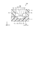

Classifications
-
- H—ELECTRICITY
- H10—SEMICONDUCTOR DEVICES; ELECTRIC SOLID-STATE DEVICES NOT OTHERWISE PROVIDED FOR
- H10P—GENERIC PROCESSES OR APPARATUS FOR THE MANUFACTURE OR TREATMENT OF DEVICES COVERED BY CLASS H10
- H10P72/00—Handling or holding of wafers, substrates or devices during manufacture or treatment thereof
- H10P72/10—Handling or holding of wafers, substrates or devices during manufacture or treatment thereof using carriers specially adapted therefor, e.g. front opening unified pods [FOUP]
-
- H—ELECTRICITY
- H10—SEMICONDUCTOR DEVICES; ELECTRIC SOLID-STATE DEVICES NOT OTHERWISE PROVIDED FOR
- H10P—GENERIC PROCESSES OR APPARATUS FOR THE MANUFACTURE OR TREATMENT OF DEVICES COVERED BY CLASS H10
- H10P95/00—Generic processes or apparatus for manufacture or treatments not covered by the other groups of this subclass
Definitions
- the present invention relates to a parts case.
- Patent Document 1 As a component case for accommodating a component such as a plurality of semiconductor chips, a semiconductor chip tray having a structure for suppressing the rattling of the component in the case and the damage of the component due to the rattling has been known.
- Patent Document 1 the component case is configured by combining a plurality of members.
- the rattling between the plurality of components may be further reduced due to the miniaturization of the components. May be required.
- one of the problems of the present invention is, for example, to obtain a parts case capable of reducing the rattling between a plurality of members constituting the parts case.
- the component case of the present invention is, for example, a component case for accommodating a plurality of components having a first surface facing the first direction and a second surface facing the opposite direction of the first direction.
- a plurality of first support surfaces that spread substantially orthogonal to the first direction and each support the first surface, and each other in one orthogonal direction that is inclined with respect to the first direction and is orthogonal to the first direction.
- a first member having two inclined surfaces that approach or separate from each other as they face the opposite direction and move toward the first direction, and the first member adjacent to the first member in the opposite direction of the first direction.
- the component case includes, for example, a third member that presses the second member in the first direction relative to the first member so that the inclined surfaces facing each other and the facing surface abut against each other. Be prepared.
- the component case includes, for example, as the third member, a plurality of members each having an engaging portion for suppressing the separation in the first direction.
- the second member projects from the edge of the opening with a base having an opening and having the two facing surfaces in a direction substantially orthogonal to the first direction. It has a plurality of protrusions having a second support surface.
- the thickness of the protrusion along the first direction is equal to or less than the thickness of the base along the first direction.
- the protrusion has a plurality of portions having different thicknesses along the first direction.
- the component has an elongated shape in a second direction orthogonal to the first direction.
- the width of the component in the first direction and the third direction orthogonal to the second direction is 2 [mm] or less.
- the first member is inclined with respect to the first direction and with respect to the first direction and the third direction orthogonal to the second direction as the two inclined surfaces.
- the second member has two first facing surfaces that extend and are in contact with each of the two first inclined surfaces.
- the first member has two second inclined surfaces that are inclined with respect to the first direction and the second direction, respectively, as the two inclined surfaces.
- the member has two second facing surfaces that extend and are in contact with each of the two second inclined surfaces.
- the component case includes, for example, a plurality of pairs of the two inclined surfaces and the two facing surfaces corresponding to the two inclined surfaces.
- the value of the elastic modulus of the first member and the value of the elastic modulus of the second member are different from each other.
- the elastic modulus of the second member is lower than the elastic modulus of the first member.
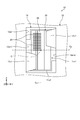
- FIG. 1 is an exemplary and schematic side view of the component case of the first embodiment.
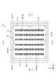
- FIG. 2 is an exemplary and schematic plan view of the first member of the first embodiment.
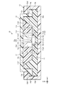
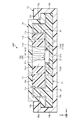
- FIG. 3 is an exemplary and schematic plan view of the first member and the second member of the first embodiment.
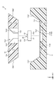
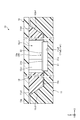
- FIG. 4 is an exemplary and schematic cross-sectional view of the component case at position IV-IV of FIG.
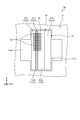
- FIG. 5 is an exemplary and schematic plan view of the parts housed in the pockets of the first member of the first embodiment.
- FIG. 6 is an exemplary and schematic disassembled side view of the first member, the component, and the second member of the first embodiment.
- FIG. 7 is an exemplary and schematic plan view of the first member, the component, and the second member of the first embodiment.
- FIG. 8 is a cross-sectional view of the component case of the reference example at the same position as in FIG.
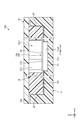
- FIG. 9 is an exemplary and schematic cross-sectional view of the component case at the IX-IX position of FIG.
- FIG. 10 is an exemplary and schematic cross-sectional view of the component case of the first modification at the same position as in FIG.
- FIG. 11 is an exemplary and schematic cross-sectional view of the component case of the second modification at the same position as in FIG.
- FIG. 12 is an exemplary and schematic cross-sectional view of the component case of the third modification at the same position as in FIG.
- the X direction is represented by an arrow X
- the Y direction is represented by an arrow Y
- the Z direction is represented by an arrow Z.
- the X, Y, and Z directions intersect and are orthogonal to each other.
- the Z direction may also be referred to as a thickness direction.
- FIG. 1 is a side view of the component case 10 of the present embodiment as viewed in the X direction.
- the component case 10 includes a first inner member 11, a second inner member 12, a first outer member 13, and a second outer member 14.
- the first inner member 11 and the second inner member 12 intersect and extend orthogonally to the Z direction, and have a thin flat shape in the Z direction.
- the second inner member 12 is located adjacent to the first inner member 11 in the direction opposite to the Z direction.
- the first inner member 11 and the second inner member 12 overlap each other in the Z direction.
- the first outer member 13 and the second outer member 14 sandwich the first inner member 11 and the second inner member 12 in the Z direction.
- the first outer member 13 has an end wall 13a, two side walls 13b, and two inward flanges 13c.
- the end wall 13a is located adjacent to the first inner member 11 in the direction opposite to the Z direction, spreads across the Z direction, and has a thin flat shape in the Z direction.
- the two side walls 13b project in the Z direction from both ends of the end wall 13a in the Y direction.
- the inward flanges 13c project in the Y direction or opposite directions in the Y direction so as to approach each other from the Z-direction ends of the side wall 13b, respectively.
- the second outer member 14 is located adjacent to the second inner member 12 in the Z direction, spreads across the Z direction, and has a thin flat shape in the Z direction.
- the outward flanges 14a located at both ends of the second outer member 14 in the Y direction are located adjacent to the inward flange 13c of the first outer member 13 in the direction opposite to the Z direction.
- the first outer member 13 holds the first inner member 11, the second inner member 12, and the outward flange 14a by the end wall 13a, the two side walls 13b, and the two inward flanges 13c. Holding like. With such a configuration, the first inner member 11, the second inner member 12, the first outer member 13, and the second outer member 14 are integrated.
- the first outer member 13 and the second outer member 14 hold the first inner member 11 and the second inner member 12 in a stacked state adjacent to each other in the Z direction.
- the inward flange 13c and the outward flange 14a suppress the separation between the first outer member 13 and the second outer member 14 in the Z direction.
- the inward flange 13c and the outward flange 14a are examples of engaging portions. It should be noted that the first outer member 13 relatively moves in the X direction with respect to the subassembly in which the first inner member 11, the second inner member 12, and the second outer member 14 are stacked in the Z direction. The assembly state shown in 1 is obtained.
- FIG. 2 is a plan view of the first inner member 11 as viewed in the direction opposite to the Z direction.
- the first inner member 11 in a plan view, has a quadrangular shape having two sides along the X direction and two sides along the Y direction.
- the first inner member 11 is provided with a plurality of recesses 11a opened in the Z direction.
- Each recess 11a is provided with a pocket 11a1 for accommodating the component 20.
- the plurality of pockets 11a1 are arranged in a matrix formed in the X direction and in the Y direction.
- FIG. 3 is a subassembly in which the first inner member 11 and the second inner member 12 are stacked adjacent to each other in the Z direction, and is viewed in the opposite direction in the Z direction in a state where the second outer member 14 is not overlapped. It is a plan view. As shown in FIG. 3, the second inner member 12 also has a quadrangular shape having two sides along the X direction and two sides along the Y direction in a plan view. The second inner member 12 is housed in the recess 11a of the first inner member 11. The first inner member 11 and the second inner member 12 are each provided with a plurality of component holding portions 10a for holding the component 20.
- the plurality of component holding portions 10a are arranged in a matrix shape arranged in the X direction and in the Y direction.
- the second inner member 12 has a plate-shaped base 12a that intersects and extends orthogonally to the Z direction, and the base 12a is provided with an opening 12a1 corresponding to each component holding portion 10a.
- FIG. 4 is a cross-sectional view of the component case 10 at the IV-IV position of FIG.
- the component 20 is housed in a pocket 11a1 provided on the bottom surface of the recess 11a.
- the pocket 11a1 may also be referred to as a housing for the component 20.
- the X-direction and Y-direction side surfaces of the pocket 11a1 function as positioning portions in the X-direction and Y-direction of the component 20.
- the component 20 is a semiconductor laser chip on-submount as an example, and has a submount 21 which is a mounting substrate and a semiconductor laser chip 22.
- the submount 21 has a bottom surface 21a and a top surface 21b.
- the length of the submount 21 in the X direction is 2 to 5 [mm]
- the width in the Y direction is 1 to 3 [mm].
- the semiconductor laser chip 22 is mounted on the top surface 21b.
- the width of the semiconductor laser chip 22 in the Y direction is 0.3 to 1 [mm].
- the component 20 is held in the component holding portion 10a, in other words, the component 20 is housed in the component case 10, the bottom surface 21a faces the opposite direction in the Z direction, and the top surface 21b faces the Z direction.
- the bottom surface 21a and the top surface 21b are parallel to each other, intersect with the Z direction, and spread orthogonally to each other.
- the bottom surface 21a is an example of the first surface
- the top surface 21b is an example of the second surface
- the opposite direction in the Z direction is an example of the first direction.
- the Z direction is an example of the opposite direction of the first direction.
- the bottom surface 21a and the top surface 21b do not have to be parallel.
- FIG. 5 is a plan view of the component 20 housed in the pocket 11a1 of the first inner member 11 as viewed in the opposite direction to the Z direction.
- the component 20 has a rectangular appearance that is long in the X direction in a plan view, and is held by the component holding portion 10a in a long posture in the X direction. Further, in the posture held by the component holding portion 10a, the semiconductor laser chip 22 extends in the X direction at the center position of the top surface 21b of the submount 21 in the Y direction.
- a first electrode 21b1 and a second electrode 21b2 that are insulated from each other by a gap 21b3 are provided on the top surface 21b.
- the semiconductor laser chip 22 is mounted on the second electrode 21b2 by, for example, soldering, so that the electrode (not shown) provided on the back surface of the semiconductor laser chip 22 and the second electrode 21b2 are electrically and mechanically connected. Is connected. Further, the electrode 22a1 provided on the surface 22a of the semiconductor laser chip 22 and the first electrode 21b1 are electrically connected by a bonding wire 23.
- the pocket 11a1 has a first portion 11a2 extending in the X direction with a predetermined width and a second portion 11a3 extending in the Y direction with a predetermined width.
- the component 20 is housed in the first portion 11a2.
- the second portion 11a3 serves as a clearance when the component 20 is taken out from the pocket 11a1 by a robot hand, tweezers, or the like (not shown).
- FIG. 6 is an exploded side view of the first inner member 11, the part 20, and the second inner member 12 as viewed in the X direction. As shown in FIG. 6, the second inner member 12 is placed on the first inner member 11 in which the component 20 is housed in the recess 11a, and the second inner member 12 is sandwiched between the first outer member 13 and the second outer member 14. The state of 4 is obtained.
- the first inner member 11 is provided with two inclined surfaces 11b1 and 11b2 inclined with respect to the Z direction and the Y direction, respectively.
- the inclined surface 11b1 is a side surface at the end portion of the recess 11a in the opposite direction in the Y direction
- the inclined surface 11b2 is a side surface at the end portion of the recess 11a in the Y direction.
- the inclined surface 11b1 faces the Z direction and the Y direction
- the inclined surface 11b2 faces the opposite directions of the Z direction and the Y direction.
- the inclined surfaces 11b1 and 11b2 are arranged in the Y direction and separated in the Y direction.
- the inclined surfaces 11b1 and 11b2 approach each other in the Y direction toward the opposite direction in the Z direction. Further, the inclined surfaces 11b1 and 11b2 are planes extending in the X direction.
- the Y direction is an example of one orthogonal direction orthogonal to the first direction.
- the second inner member 12 is provided with two inclined surfaces 12b1 and 12b2 inclined with respect to the Z direction and the Y direction, respectively.
- the inclined surface 12b1 is provided at the end of the base 12a in the opposite direction to the Y direction
- the inclined surface 12b2 is provided at the end of the base 12a in the Y direction.
- the inclined surface 12b1 faces the opposite direction in the Z direction and the opposite direction in the Y direction
- the inclined surface 12b2 faces the opposite direction in the Z direction and the Y direction.
- the inclined surfaces 12b1 and 12b2 are arranged in the Y direction and separated in the Y direction.
- the inclined surfaces 12b1 and 12b2 approach each other in the Y direction toward the opposite direction in the Z direction.
- the inclined surfaces 12b1 and 12b2 are planes extending in the X direction.
- the inclined surface 11b1 and the inclined surface 12b1 are in contact with each other and face each other, and are in contact with the inclined surface 11b2.
- the inclined surfaces 12b2 are in contact with each other and face each other.
- the first inner member 11 and the second inner member 12 are positioned in the Z direction as well as in the Y direction.
- first outer member 13 and the second outer member 14 elastically press the first inner member 11 and the second inner member 12 in the Z direction.
- the inclined surface 11b1 and the inclined surface 12b1 are pressed against each other, and the inclined surface 11b2 and the inclined surface 12b2 are pressed against each other. That is, the first outer member 13 and the second outer member 14 sandwich the first inner member 11 and the second inner member 12 in the Z direction, whereby the first inner member 11 and the second inner member 12 are sandwiched in the Z direction. And the position shift in the Y direction is suppressed.
- the first outer member 13 and the second outer member 14 are examples of two members constituting the third member.
- FIG. 7 is a plan view of the subassemblies of the first inner member 11, the part 20, and the second inner member 12 as viewed in the opposite directions in the Z direction.
- two arms 12c1 and 12c2 project from the edge 12a11 of the opening 12a1 provided in the second inner member 12 in a direction intersecting the Z direction and substantially orthogonal to the Z direction. ..
- One arm 12c1 projects in the Y direction from the edge 12a11 which is the end in the opposite direction of the Y direction of the opening 12a1, and the other arm 12c2 is from the edge 12a12 which is the end in the opposite direction in the Y direction of the opening 12a1. It protrudes in the opposite direction of the Y direction.
- the two arms 12c1 and 12c2 are positioned apart from the semiconductor laser chip 22 and the bonding wire 23 so as not to interfere with the semiconductor laser chip 22 and the bonding wire 23.
- the two arms 12c1, 12c2 and the first portion 11a2 of the pocket 11a1 are the center lines along the X direction and the center lines along the Y direction of the component 20 held by the component holding portion 10a in the plan view of FIG. 7. It is substantially point-symmetrical with respect to the center point C, which is the intersection of Cy. Therefore, even when the component 20 is housed in the posture inverted in the X direction or the Y direction with respect to the posture shown in FIG. 7, the semiconductor laser chip 22, the bonding wire 23, and the arms 12c1, 12c2 are housed in the first portion 11a2. Does not interfere with. In other words, the component 20 can be accommodated in the first portion 11a2 in both the posture shown in FIG. 7 and the posture in which the posture shown in FIG. 7 is inverted in the X direction or the Y direction.
- the bottom surface 21a of the submount 21 is the bottom surface 11a4 of the pocket 11a1.
- the top surface 21b of the submount 21 faces and is in contact with the back surface 12d of the arms 12c1 and 12c2.
- the first inner member 11 is an example of the first member
- the second inner member 12 is an example of the second member.
- the arms 12c1 and 12c2 are examples of protrusions
- the bottom surface 21a is an example of a first surface
- the top surface 21b is an example of a second surface
- the bottom surface 11a4 is an example of a first support surface.
- the back surface 12d is an example of the second support surface.
- FIG. 8 shows a reference example component case 10R in which the first inner member 11 and the second inner member 12 are provided with vertical surfaces 11c and 12g perpendicular to the Y direction and facing each other for positioning in the Y direction.
- FIG. 8 It is a cross-sectional view at the same position as FIG.
- the first inner member 11 and the second inner member 12 are smoothly brought in and out of the component case 10a along the Z direction when the component 20 is accommodated or removed from the component holding portion 10a.
- this gap g1 is usually set to about 0.2 to 0.5 [mm].
- the gap between the pocket 11a1 and the component 20 is set to about 0.2 to 0.5 [mm]. Therefore, the rattling of the component 20 and the second inner member 12 in the Y direction in the component case 10R is usually 0.4 to 1 [mm], and in such a case, on the top surface 21b of the submount 21.
- the semiconductor laser chip 22 mounted on the top surface 21b interferes with the portion of the second inner member 12 such as the arms 12c1 and 12c2 located on the top surface 21b, and the risk of damaging the semiconductor laser chip 22 increases. ..
- the two inclined surfaces 11b1 and 11b2 face each other in the opposite direction in the Y direction, and approach each other in the Y direction toward the opposite direction in the Z direction.
- the inclined surface 12b1 extends and contacts along the inclined surface 11b1
- the inclined surface 12b2 extends and contacts along the inclined surface 11b2.
- the first inner member 11 and the second inner member 12 are in contact with each other with almost no gap, and are positioned in the Z direction and the Y direction without any rattling.
- inclining in the Z direction and inclining in the opposite direction (first direction) in the Z direction are equivalent.
- the Y direction is an example of an orthogonal direction and a third direction
- the inclined surfaces 11b1 and 11b2 are examples of the first inclined surface
- the inclined surfaces 12b1 and 12b2 are examples of the facing surface and the first facing surface.
- the configuration for reducing the rattling by the two inclined surfaces 11b1 and 11b2 is It can be said that it is more effective when the length (width) in the lateral direction orthogonal to the Z direction of the component 20, that is, in the Y direction in the present embodiment is 2 [mm] or less.
- the width of the component 20 is 2 [mm] or less
- the length (width) of the pocket 11a1 in the Y direction in other words, the distance between the side surfaces on both sides in the Y direction is, for example, 3 [mm] or less.
- it is about 0.2 to 0.5 [mm] larger than the width of the component 20.
- the first inner member 11 and the second inner member 12 are made of, for example, polycarbonate or a synthetic resin material such as ABS resin, polypropylene, or polystyrene, respectively. Further, the first inner member 11 and the second inner member 12 may be made of different materials, and as an example, the second inner member 12 is made of a material having a lower elastic modulus than the first inner member 11. It is preferable to have. Further, it is preferable that the arms 12c1 and 12c2 have a portion where the thickness along the Z direction is thinner than the thickness along the Z direction of the base 12a. Further, the thickness of the arms 12c1 and 12c2 along the Z direction may be different depending on the position in the Y direction.
- the arms 12c1 and 12c2 each have a plurality of portions having different thicknesses.
- the thickness of the arms 12c1 and 12c2 along the Z direction is gradually reduced, that is, thinned from the root to the tip.
- the first inner member 11 and the first inner member 11 and 12c2 are elastically deformed by the elastic deformation of the arms 12c1 and 12c2 of the second inner member 12. It is possible to suppress an excessive force from acting on the component 20 from the second inner member 12.
- the magnitude of the force acting on the component 20 from the first inner member 11 and the second inner member 12 is appropriately adjusted according to the specifications such as the shape, dimensions, and material of the first inner member 11 and the second inner member 12. can do.
- the thickness along the Z direction is equivalent to the thickness along the opposite direction of the Z direction, and is an example of the thickness along the first direction.
- the first inner member 11 and the second inner member 12 may be made of the same material or may be made by injection molding. Further, the thickness of the arms 12c1 and 12c2 does not have to be thinned toward the tip.
- FIG. 9 is a cross-sectional view of the component case 10 at the IX-IX position of FIG.
- the first inner member 11 is provided with two inclined surfaces 11b3 and 11b4 inclined with respect to the Z direction and the X direction, respectively.
- the inclined surface 11b3 is a side surface at the end portion of the recess 11a in the opposite direction in the X direction
- the inclined surface 11b4 is a side surface at the end portion of the recess 11a in the X direction.
- the inclined surface 11b3 faces the Z direction and the X direction
- the inclined surface 11b4 faces the opposite directions of the Z direction and the X direction.
- the inclined surfaces 11b3 and 11b4 are arranged in the X direction and separated in the X direction.
- the inclined surfaces 11b3 and 11b4 approach each other in the X direction toward the opposite direction in the Z direction. Further, the inclined surfaces 11b3 and 11b4 are planes extending in the Y direction.
- the X direction is an example of one orthogonal direction orthogonal to the first direction.
- the second inner member 12 is provided with two inclined surfaces 12b3 and 12b4 inclined with respect to the Z direction and the X direction, respectively.
- the inclined surface 12b3 is provided at the end of the base 12a in the direction opposite to the X direction
- the inclined surface 12b4 is provided at the end of the base 12a in the X direction.
- the inclined surface 12b3 faces the opposite direction in the Z direction and the opposite direction in the X direction
- the inclined surface 12b4 faces the opposite direction in the Z direction and the X direction.
- the inclined surfaces 12b3 and 12b4 are arranged in the X direction and separated in the X direction.
- the inclined surfaces 12b3 and 12b4 approach each other in the X direction toward the opposite direction in the Z direction.
- the inclined surfaces 12b3 and 12b4 are planes extending in the Y direction.
- the two inclined surfaces 11b3 and 11b4 face each other in the opposite direction in the X direction and approach each other in the X direction as they go in the opposite directions in the Z direction, and the first inner member 11 and the second inner member 12
- the inclined surface 12b3 extends and contacts along the inclined surface 11b3
- the inclined surface 12b4 extends and contacts along the inclined surface 11b4.
- the first inner member 11 and the second inner member 12 are in contact with each other with almost no gap, and are positioned in the Z direction and the X direction without any rattling.
- the X direction is an example of an orthogonal direction and a second direction
- an inclined surface 11b3, 11b4 is an example of a second inclined surface
- an inclined surface 12b3, 12b4 is an example of a facing surface and a second facing surface.
- the first inner member 11 has two inclined surfaces 11b1 and 11b2. These inclined surfaces 11b1 and 11b2 face each other in the Y direction and face the opposite direction in the Z direction (first direction) and the Y direction orthogonal to the opposite direction in the Z direction (the orthogonal direction in the first direction). They are getting closer to each other as they tilt and go in the opposite direction of the Z direction.
- the second inner member 12 has two inclined surfaces 12b1 and 12b2 (opposing surfaces). These inclined surfaces 12b1 and 12b2 extend and are in contact with each of the two inclined surfaces 11b1 and 11b2.
- the first inner member 11 and the second inner member 12 are in the Z direction and the Y direction. It is possible to suppress rattling, that is, rattling in the first direction and the orthogonal direction.
- first outer member 13 and the second outer member 14 have the second inner member 12 so that the inclined surfaces 11b1, 11b2 and the inclined surfaces 12b1, 12b2 facing each other abut against each other. It is pressed in the direction opposite to the Z direction relative to the first inner member 11.
- the inclined surfaces 11b1, 11b2 and the corresponding inclined surfaces 12b1, 12b2 are in contact with each other, so that the rattling between the first inner member 11 and the second inner member 12 is suppressed. Can be maintained more easily or more reliably.
- the arms 12c1 and 12c2 protruding portions have a portion where the thickness along the Z direction, that is, the thickness along the first direction is thinner than the thickness along the Z direction of the base 12a. is doing.
- the arms 12c1 and 12c2 have a plurality of portions having different thicknesses along the Z direction.
- the elastic modulus values of the first inner member 11 and the second inner member 12 are different from each other.
- the elastic modulus of the second inner member 12 is the elasticity of the first inner member 11. Lower than the coefficient.
- the component 20 has an elongated shape in the X direction (second direction) orthogonal to the Z direction.
- the first inner member 11 has two inclined surfaces 11b1 and 11b2 (first inclined surfaces) inclined with respect to the Z direction and the Y direction (third direction), and the second inner member member 11.
- Reference numeral 12 has two inclined surfaces 12b1, 12b2 (first facing surfaces) extending along and in contact with each of the two inclined surfaces 11b1, 11b2.
- the inclined surfaces 11b1, 11b2 and the corresponding inclined surfaces 12b1, 12b2 are in contact with each other, so that the first inner member 11 and the second inner member 12 rattle in the Z direction and the Y direction. Can be suppressed. Therefore, according to such a configuration, for example, even when the component 20 is elongated in the X direction and the width in the Y direction is short, the first inner member 11 and the second inner member 12 rattle in the Y direction. It can be suppressed more reliably, and interference between the arms 12c1 and 12c2 and the semiconductor laser chip 22 and the bonding wire 23 can be more reliably avoided.
- the first inner member 11 has two inclined surfaces 11b3 and 11b4 (second inclined surfaces) inclined with respect to the Z direction and the X direction (second direction), and the second inner member member 11.
- Reference numeral 12 has two inclined surfaces 12b3, 12b4 (second facing surfaces) extending along and in contact with each of the two inclined surfaces 11b3, 11b4.
- the first inner member 11 and the second inner member 12 are in the Z direction and the X direction. It can suppress rattling.
- the component case 10 has a pair of two inclined surfaces 11b1, 11b2 and two inclined surfaces 12b1, 12b2 corresponding thereto, two inclined surfaces 11b3, 11b4 and two corresponding inclined surfaces. It is provided with a pair with an inclined surface 12b3 and 12b4. That is, the component case 10 includes a plurality of pairs of two inclined surfaces and two corresponding facing surfaces.
- rattling in the first direction of the first inner member 11 and the second inner member 12 and rattling in a plurality of directions orthogonal to the first direction are suppressed. Can be done.
- FIG. 10 is a cross-sectional view of the component case 10A of the first modification at the same position as that of FIG.
- the component case 10A of the present modification has the same configuration as the component case 10 of the first embodiment except for the portion shown in FIG.
- the inclined surfaces 11b3, 11b4, 12b3, 12b4 are not provided.
- a gap g2 is formed between the second inner member 12 and the first inner member 11 at both ends in the X direction.
- the component case 10A can be made smaller in the X direction because the inclined surfaces 11b3, 11b4, 12b3, 12b4 are not provided.
- FIG. 11 is a cross-sectional view of the component case 10B of the second modification at the same position as in FIG.
- the component case 10B of the present modification has the same configuration as the component case 10 of the first embodiment except for the portion shown in FIG.
- thin-walled portions 12e are provided at the root portions of the arms 12c1 and 12c2, respectively.
- the arms 12c1 and 12c2 are more likely to be elastically deformed as compared with the case where the thin-walled portion 12e is not provided, and the force acting on the component 20 can be made smaller.
- the thickness of the arms 12c1 and 12c2 changes along the Z direction.
- the thin-walled portion 12e can also be referred to as an easily deformable portion.
- FIG. 12 is a cross-sectional view of the component case 10C of the third modification at the same position as in FIG.
- the component case 10C of this modification includes a second inner member 12C in which the second inner member 12 and the second outer member 14 of the first embodiment are integrated.
- the first outer member 13 functions as the third member.
- FIG. 12 shows only the end portion of the component case 10C in the opposite direction to the Y direction, but the component case 10C has a mirror image relationship with the configuration shown in FIG. 12 even at the end portion in the Y direction. It has a symmetrical shape.
- the second inner member 12C has outward flanges 12f located at both ends in the Y direction.
- the outward flange 12f is positioned adjacent to the inward flange 13c of the first outer member 13 in the direction opposite to the Z direction.
- the first outer member 13 is provided with the first inner member 11 and the second inner member by means of the end wall 13a, the two side walls 13b, and the two inward flanges 13c (only one is shown in FIG. 12). It holds the 12C so as to hold it.
- the first inner member 11, the second inner member 12C, and the first outer member 13 are integrated.
- the first outer member 13 holds the first inner member 11 and the second inner member 12C in a stacked state adjacent to each other in the Z direction.
- the first outer member 13 relatively moves in the X direction with respect to the subassembly in which the first inner member 11 and the second inner member 12C are stacked in the Z direction, so that FIG. 12 shows.
- the indicated assembly state is obtained. Even in such a configuration, the same effect as that of the first embodiment can be obtained. Further, according to this modification, there is an advantage that the number of parts can be reduced.
- the component is not limited to the semiconductor laser element, and the present invention can be similarly applied to an electric component, an optical component, and other components as well as an electronic component such as a semiconductor chip.
- the positions and orientations of the inclined surface and the facing surface are not limited to the above-described embodiments and modifications, and may take various forms.
- the third member that integrates the first member and the second member is not limited to the slide type component exemplified in the above embodiment, and may be a member of another form such as a screw or a clamp. There may be. Further, the third member may have three or more members, or each may have an engaging portion having a form different from that of the flange.
- the present invention can be used for a parts case.
- Electrode 23 Bonding wire g1, g2 ... Gap C ... Center point Cx ... Center line Cy ... Center line X ... Direction (orthogonal) Direction, second direction) Y ... direction (orthogonal direction, third direction) Z ... direction (opposite direction of the first direction)
Landscapes
- Optical Couplings Of Light Guides (AREA)
- Piezo-Electric Or Mechanical Vibrators, Or Delay Or Filter Circuits (AREA)
- Packaging Frangible Articles (AREA)
- Container, Conveyance, Adherence, Positioning, Of Wafer (AREA)
Abstract
部品ケースは、それぞれ第一方向を向いた第一面と第一方向の反対方向を向いた第二面とを有した複数の部品を収容する部品ケースであって、第一方向と略直交して広がり、それぞれ第一面を支持する複数の第一支持面と、それぞれ第一方向に対して傾斜するとともに第一方向と直交する一つの直交方向において互いに反対方向を向き第一方向に向かうにつれて互いに近付くかあるいは離間する二つの傾斜面と、を有した第一部材と、第一部材に対して第一方向の反対方向に隣接して第一方向と略直交して広がり、それぞれ第二面を支持する複数の第二支持面と、二つの傾斜面のそれぞれに沿って延びるとともに接した二つの対向面と、を有した第二部材と、を備える。
Description
本発明は、部品ケースに関する。
従来、複数の半導体チップのような部品を収容する部品ケースとして、ケース内での部品のがたつきや当該がたつきによる部品の損傷を抑制する構造を備えた半導体チップトレイが、知られている(特許文献1)。特許文献1では、部品ケースは、複数の部材を組み合わせて構成されている。
特許文献1のように、部品ケースが複数の部材を組み合わせて構成されている場合にあっては、例えば、部品の小型化等に伴い、複数の部材間のがたつきをより小さくすることが必要となる場合がある。
そこで、本発明の課題の一つは、例えば、部品ケースを構成する複数の部材間のがたつきをより小さくすることが可能な部品ケースを得ること、である。
本発明の部品ケースは、例えば、それぞれ第一方向を向いた第一面と前記第一方向の反対方向を向いた第二面とを有した複数の部品を収容する部品ケースであって、前記第一方向と略直交して広がり、それぞれ前記第一面を支持する複数の第一支持面と、それぞれ前記第一方向に対して傾斜するとともに前記第一方向と直交する一つの直交方向において互いに反対方向を向き前記第一方向に向かうにつれて互いに近付くかあるいは離間する二つの傾斜面と、を有した第一部材と、前記第一部材に対して前記第一方向の反対方向に隣接して前記第一方向と略直交して広がり、それぞれ前記第二面を支持する複数の第二支持面と、前記二つの傾斜面のそれぞれに沿って延びるとともに接した二つの対向面と、を有した第二部材と、を備える。
また、前記部品ケースは、例えば、互いに面した前記傾斜面と前記対向面とが突き当たるように前記第二部材を前記第一部材に対して相対的に前記第一方向に押圧する第三部材を備える。
また、前記部品ケースは、例えば、前記第三部材として、前記第一方向に離れるのを抑制する係合部をそれぞれ有した複数の部材を備える。
また、前記部品ケースでは、例えば、前記第二部材は、開口が設けられ前記二つの対向面を有したベースと、それぞれ前記開口の縁から前記第一方向と略直交する方向に突出するとともに前記第二支持面を有した複数の突出部と、を有する。
また、前記部品ケースでは、例えば、前記突出部の前記第一方向に沿った厚さは、前記ベースの前記第一方向に沿った厚さ以下である。
また、前記部品ケースでは、例えば、前記突出部は、前記第一方向に沿った厚さが異なる複数の部位を有する。
また、前記部品ケースでは、例えば、前記部品は、前記第一方向と直交した第二方向に細長い形状を有する。
また、前記部品ケースでは、例えば、前記部品の、前記第一方向および前記第二方向と直交する第三方向の幅が、2[mm]以下である。
また、前記部品ケースでは、例えば、前記第一部材は、前記二つの傾斜面として、それぞれ前記第一方向に対して傾斜するとともに前記第一方向および前記第二方向と直交する第三方向に対して傾斜する二つの第一傾斜面を有し、前記第二部材は、前記二つの第一傾斜面のそれぞれに沿って延びるとともに接した二つの第一対向面、を有する。
また、前記部品ケースでは、例えば、前記第一部材は、前記二つの傾斜面として、それぞれ前記第一方向および前記第二方向に対して傾斜する二つの第二傾斜面を有し、前記第二部材は、前記二つの第二傾斜面のそれぞれに沿って延びるとともに接した二つの第二対向面、を有する。
また、前記部品ケースは、例えば、前記二つの傾斜面と当該二つの傾斜面に対応する前記二つの対向面との複数のペアを備える。
また、前記部品ケースでは、例えば、前記第一部材の弾性係数の値と前記第二部材の弾性係数の値とが互いに異なる。
また、前記部品ケースでは、例えば、前記第二部材の弾性係数は、前記第一部材の弾性係数よりも低い。
本発明によれば、例えば、部品ケースを構成する複数の部材間のがたつきをより小さくすることが可能な部品ケースを得ることができる。
以下、本発明の例示的な実施形態および変形例が開示される。以下に示される実施形態および変形例の構成、ならびに当該構成によってもたらされる作用および結果(効果)は、一例である。本発明は、以下の実施形態および変形例に開示される構成以外によっても実現可能である。また、本発明によれば、構成によって得られる種々の効果(派生的な効果も含む)のうち少なくとも一つを得ることが可能である。
以下に示される実施形態および変形例は、同様の構成を備えている。よって、各実施形態および変形例の構成によれば、当該同様の構成に基づく同様の作用および効果が得られる。また、以下では、それら同様の構成には同様の符号が付与されるとともに、重複する説明が省略される場合がある。
本明細書において、序数は、部品や部位等を区別するために便宜上付与されており、優先順位や順番を示すものではない。
また、各図において、X方向を矢印Xで表し、Y方向を矢印Yで表し、Z方向を矢印Zで表す。X方向、Y方向、およびZ方向は、互いに交差するとともに互いに直交している。なお、Z方向は、厚さ方向とも称されうる。
[第1実施形態]
図1は、本実施形態の部品ケース10の、X方向に見た側面図である。部品ケース10は、第一インナ部材11、第二インナ部材12、第一アウタ部材13、および第二アウタ部材14を備えている。
図1は、本実施形態の部品ケース10の、X方向に見た側面図である。部品ケース10は、第一インナ部材11、第二インナ部材12、第一アウタ部材13、および第二アウタ部材14を備えている。
第一インナ部材11および第二インナ部材12は、Z方向と交差しかつ直交して広がっており、Z方向に薄い扁平な形状を有している。第二インナ部材12は、第一インナ部材11に対してZ方向の反対方向に隣接して位置している。第一インナ部材11と第二インナ部材12とは、Z方向に重なっている。
第一アウタ部材13および第二アウタ部材14は、第一インナ部材11と第二インナ部材12とをZ方向に挟んでいる。第一アウタ部材13は、端壁13aと、二つの側壁13bと、二つの内向きフランジ13cと、を有している。端壁13aは、第一インナ部材11に対してZ方向の反対方向に隣接して位置し、Z方向と交差して広がり、Z方向に薄い扁平な形状を有している。二つの側壁13bは、端壁13aのY方向の両端からZ方向に突出している。内向きフランジ13cは、それぞれ、側壁13bのZ方向の端部から互いに近付くようにY方向またはY方向の反対方向に突出している。また、第二アウタ部材14は、第二インナ部材12に対してZ方向に隣接して位置し、Z方向と交差して広がり、Z方向に薄い扁平な形状を有している。第二アウタ部材14のY方向の両端に位置された外向きフランジ14aは、第一アウタ部材13の内向きフランジ13cに対して、Z方向の反対方向に隣接して位置されている。このような構成により、第一アウタ部材13は、端壁13a、二つの側壁13b、および二つの内向きフランジ13cにより、第一インナ部材11、第二インナ部材12、および外向きフランジ14aを抱え込むように保持している。このような構成により、第一インナ部材11、第二インナ部材12、第一アウタ部材13、および第二アウタ部材14が、一体化している。言い換えると、第一アウタ部材13および第二アウタ部材14は、第一インナ部材11および第二インナ部材12をZ方向に隣接して積み重なった状態に保持している。このように、本実施形態では、内向きフランジ13cと外向きフランジ14aとが、第一アウタ部材13と第二アウタ部材14とがZ方向に離間するのを抑制している。内向きフランジ13cおよび外向きフランジ14aは、係合部の一例である。なお、第一インナ部材11、第二インナ部材12、および第二アウタ部材14がZ方向に積み重ねられたサブアセンブリに対して、第一アウタ部材13がX方向に相対的移動することにより、図1に示すアセンブリ状態が得られる。
図2は、第一インナ部材11のZ方向の反対方向に見た平面図である。図2に示されるように、第一インナ部材11は、平面視では、X方向に沿う二つの辺とY方向に沿う二つの辺とを有した四角形状の形状を有している。第一インナ部材11には、Z方向に向けて開口した複数の凹部11aが設けられている。凹部11aにはそれぞれ部品20を収容するポケット11a1が設けられている。複数のポケット11a1は、X方向に並ぶとともにY方向に並んだマトリクス状に配置されている。
図3は、第一インナ部材11と第二インナ部材12がZ方向に隣接して積み重なったサブアセンブリの、第二アウタ部材14が重ねられていない状態での、Z方向の反対方向に見た平面図である。図3に示されるように、第二インナ部材12も、平面視では、X方向に沿う二つの辺とY方向に沿う二つの辺とを有した四角形状の形状を有している。第二インナ部材12は、第一インナ部材11の凹部11a内に収容されている。第一インナ部材11および第二インナ部材12には、それぞれ部品20を保持する複数の部品保持部10aが設けられている。複数の部品保持部10aは、X方向に並ぶとともにY方向に並んだマトリクス状に配置されている。第二インナ部材12は、Z方向と交差しかつ直交して広がる板状のベース12aを有し、当該ベース12aには、各部品保持部10aに対応して、開口12a1が設けられている。第二アウタ部材14が重ねられていない第一インナ部材11と第二インナ部材12とのサブアセンブリをZ方向の反対方向に見ることにより、開口12a1を通じて、各部品保持部10aにおける部品20の有無を視認することができる。
図4は、図3のIV-IV位置での部品ケース10の断面図である。図4に示されるように、部品20は、凹部11aの底面に設けられたポケット11a1に収容されている。ポケット11a1は、部品20の収容部とも称されうる。また、ポケット11a1のX方向およびY方向の側面は、部品20のX方向およびY方向の位置決め部として機能する。
部品20は、本実施形態では、一例として、半導体レーザチップオンサブマウントであり、実装基板であるサブマウント21と、半導体レーザチップ22と、を有している。サブマウント21は、底面21aと頂面21bとを有している。一例として、サブマウント21のX方向の長さは2~5[mm]、Y方向の幅は1~3[mm]である。半導体レーザチップ22は、頂面21b上に実装されている。一例として、半導体レーザチップ22のY方向の幅は0.3~1[mm]である。
部品20が部品保持部10aに保持された姿勢、言い換えると部品20が部品ケース10に収容された姿勢で、底面21aはZ方向の反対方向を向き、頂面21bはZ方向を向いている。本実施形態では、一例として、底面21aおよび頂面21bは、平行であり、それぞれZ方向と交差するとともに直交して広がっている。底面21aは、第一面の一例であり、頂面21bは、第二面の一例であり、Z方向の反対方向は、第一方向の一例である。言い換えると、Z方向は、第一方向の反対方向の一例である。なお、底面21aおよび頂面21bは平行で無くてもよい。
図5は、第一インナ部材11のポケット11a1に収容された部品20の、Z方向の反対方向に見た平面図である。図5に示されるように、部品20は、平面視ではX方向に長い長方形状の外観を呈しており、部品保持部10aには、X方向に長い姿勢で保持されている。また、部品保持部10aに保持された姿勢において、半導体レーザチップ22は、サブマウント21の頂面21bのY方向の中央位置において、X方向に延びている。
頂面21b上には、ギャップ21b3により互いに絶縁された第一電極21b1と第二電極21b2とが設けられている。半導体レーザチップ22は、第二電極21b2上に例えばはんだ付けなどにより実装されており、これにより半導体レーザチップ22の裏面に設けられた電極(不図示)と第二電極21b2とが電気的かつ機械的に接続されている。また、半導体レーザチップ22の表面22aに設けられた電極22a1と第一電極21b1との間は、ボンディングワイヤ23によって電気的に接続されている。
ポケット11a1は、所定幅でX方向に延びた第一部位11a2と、所定幅でY方向に延びた第二部位11a3と、を有している。部品20は、第一部位11a2に収容されている。第二部位11a3は、部品20をロボットのハンドやピンセット等(いずれも不図示)によって部品20をポケット11a1から取り出す際のクリアランスとなる。
図6は、第一インナ部材11、部品20、および第二インナ部材12の、X方向に見た分解側面図である。図6に示されるように、凹部11aに部品20が収容された第一インナ部材11上に、第二インナ部材12を載せ、第一アウタ部材13および第二アウタ部材14によって挟むことにより、図4の状態が得られる。
図4,6から明らかとなるように、第一インナ部材11には、それぞれZ方向およびY方向に対して傾斜した二つの傾斜面11b1,11b2が設けられている。傾斜面11b1は、凹部11aのY方向の反対方向の端部における側面であり、傾斜面11b2は、凹部11aのY方向の端部における側面である。傾斜面11b1は、Z方向およびY方向を向き、傾斜面11b2は、Z方向およびY方向の反対方向を向いている。傾斜面11b1,11b2は、Y方向に並ぶとともにY方向に離間している。傾斜面11b1,11b2は、Z方向の反対方向に向かうにつれて互いにY方向に近付いている。また、傾斜面11b1,11b2は、X方向にも延びた平面である。Y方向は、第一方向と直交する一つの直交方向の一例である。
他方、第二インナ部材12には、それぞれZ方向およびY方向に対して傾斜した二つの傾斜面12b1,12b2が設けられている。傾斜面12b1は、ベース12aのY方向の反対方向の端部に設けられ、傾斜面12b2は、ベース12aのY方向の端部に設けられている。傾斜面12b1は、Z方向の反対方向およびY方向の反対方向を向き、傾斜面12b2は、Z方向の反対方向およびY方向を向いている。傾斜面12b1,12b2は、Y方向に並ぶとともにY方向に離間している。傾斜面12b1,12b2は、Z方向の反対方向に向かうにつれて互いにY方向に近付いている。また、傾斜面12b1,12b2は、X方向にも延びた平面である。
そして、図4に示されるように、第一インナ部材11と第二インナ部材12とがZ方向に重なった状態において、傾斜面11b1と傾斜面12b1とが互いに接するとともに面し、傾斜面11b2と傾斜面12b2とが互いに接するとともに面する。これにより、第一インナ部材11と第二インナ部材12とは、Z方向に位置決めされるとともに、Y方向にも位置決めされる。
さらに、第一アウタ部材13および第二アウタ部材14は、第一インナ部材11と第二インナ部材12とを弾性的にZ方向に押圧している。これにより、傾斜面11b1と傾斜面12b1とは互いに押し合い、傾斜面11b2と傾斜面12b2とは互いに押し合うことになる。すなわち、第一アウタ部材13および第二アウタ部材14は、第一インナ部材11と第二インナ部材12とをZ方向に挟むことにより、第一インナ部材11と第二インナ部材12とのZ方向およびY方向への位置ずれを抑制している。第一アウタ部材13および第二アウタ部材14は、第三部材を構成する二つの部材の一例である。
図7は、第一インナ部材11、部品20、および第二インナ部材12のサブアセンブリの、Z方向の反対方向に見た平面図である。図7に示されるように、第二インナ部材12に設けられた開口12a1の縁12a11からは、Z方向と交差しかつZ方向と略直交する方向に、二つのアーム12c1,12c2が突出している。一つのアーム12c1は、開口12a1のY方向の反対方向の端部となる縁12a11からY方向に突出し、もう一つのアーム12c2は、開口12a1のY方向の反対方向の端部となる縁12a12からY方向の反対方向に突出している。これら二つのアーム12c1,12c2は、半導体レーザチップ22およびボンディングワイヤ23から離れ、半導体レーザチップ22およびボンディングワイヤ23と干渉しないように位置されている。また、二つのアーム12c1,12c2およびポケット11a1の第一部位11a2は、図7の平面視において、部品保持部10aに保持された部品20のX方向に沿う中心線CxおよびY方向に沿う中心線Cyの交点である中心点Cに対して、略点対称である。したがって、第一部位11a2において、部品20が図7の姿勢に対してX方向またはY方向に反転した姿勢に収容された場合にあっても、半導体レーザチップ22およびボンディングワイヤ23とアーム12c1,12c2とは干渉しない。言い換えると、部品20は、図7に示される姿勢と、図7に示される姿勢とはX方向またはY方向に反転した姿勢と、の双方で、第一部位11a2に収容することができる。
また、図4に示されるように、部品20がポケット11a1に収容された状態、言い換えると部品20が部品保持部10aに保持された状態において、サブマウント21の底面21aは、ポケット11a1の底面11a4に面するとともに接し、サブマウント21の頂面21bは、アーム12c1,12c2の裏面12dに面するとともに接している。第一インナ部材11、第二インナ部材12、および部品20が指定された寸法公差範囲内で製造された場合にあっては、底面21aと底面11a4とが接するとともに、頂面21bと裏面12dとが接するよう、構成されている。これにより、部品20の部品保持部10aにおけるZ方向の位置ずれを抑制することができるとともに、底面21aと底面11a4との接触による摩擦、ならびに頂面21bと裏面12dとの接触による摩擦により、Z方向と交差する他方向への位置ずれも抑制することができる。第一インナ部材11は、第一部材の一例であり、第二インナ部材12は、第二部材の一例である。また、アーム12c1,12c2は、突出部の一例であり、底面21aは、第一面の一例であり、頂面21bは、第二面の一例であり、底面11a4は、第一支持面の一例であり、裏面12dは、第二支持面の一例である。
図8は、仮に、Y方向における位置決めのため、第一インナ部材11および第二インナ部材12に、Y方向と垂直で互いに対向する垂直面11c,12gをそれぞれ設けた参考例の部品ケース10Rの、図4と同等位置での断面図である。部品ケース10Rにあっては、部品20の部品保持部10aに対する収容時や取出時において、第一インナ部材11と第二インナ部材12とをZ方向に沿って円滑に近づけたり離したりするため、それら垂直面11c,12gの間にY方向に隙間g1を設ける必要がある。また、第一インナ部材11および第二インナ部材12を製作する際の寸法公差としても、隙間g1を設ける必要がある。よって、この隙間g1は、通常、0.2~0.5[mm]程度に設定される。他方、ポケット11a1への部品20の収容および取り出しを円滑に行うために、ポケット11a1と部品20との間の隙間は、0.2~0.5[mm]程度に設定されている。したがって、部品ケース10Rにおける、部品20と第二インナ部材12とのY方向のがたつきは、通常、0.4~1[mm]となり、このような場合、サブマウント21の頂面21b上に実装された半導体レーザチップ22と、頂面21b上に位置するアーム12c1,12c2のような第二インナ部材12の部位とが干渉し、半導体レーザチップ22を破損する虞が、高くなってしまう。
この点、本実施形態では、上述したように、二つの傾斜面11b1,11b2は、Y方向において互いに反対方向を向き、Z方向の反対方向に向かうにつれて互いにY方向に近付いており、第一インナ部材11と第二インナ部材12とがZ方向に重なった状態において、傾斜面12b1は傾斜面11b1に沿って延びるとともに接し、傾斜面12b2は傾斜面11b2に沿って延びるとともに接する。これにより、第一インナ部材11と第二インナ部材12とは、略隙間無く当接し、略がたつくことなくZ方向およびY方向に位置決めされる。なお、Z方向に対して傾斜することと、Z方向の反対方向(第一方向)に対して傾斜することとは、等価である。Y方向は、直交方向および第三方向の一例であり、傾斜面11b1,11b2は、第一傾斜面の一例であり、傾斜面12b1,12b2は、対向面および第一対向面の一例である。
また、上述した部品ケース10Rのような垂直面11c,12gを設けた場合のがたつきが最大1[mm]程度となることから、二つの傾斜面11b1,11b2によりがたつきを減らす構成は、部品20のZ方向と直交する短手方向、すなわち本実施形態ではY方向の長さ(幅)が、2[mm]以下であるような場合において、より効果的であると言える。また、部品20の幅が2[mm]以下である場合、ポケット11a1のY方向の長さ(幅)、言い換えるとY方向の両側の側面間の距離は、例えば、3[mm]以下であるとともに部品20の幅よりも0.2~0.5[mm]程度大きい。
ここで、本実施形態では、第一インナ部材11および第二インナ部材12は、それぞれ、例えば、ポリカーボネートや、ABS樹脂、ポリプロピレン、ポリスチレンのような合成樹脂材料で作られている。また、第一インナ部材11および第二インナ部材12は、それぞれ異なる材料で作られても良く、一例として、第二インナ部材12は、第一インナ部材11よりも弾性係数の低い材料で作られているのが好ましい。また、アーム12c1,12c2は、Z方向に沿った厚さがベース12aのZ方向に沿った厚さよりも薄い部分を有しているのが好ましい。また、アーム12c1,12c2のZ方向に沿った厚さは、Y方向の位置に応じて異なっていてもよい。すなわち、アーム12c1,12c2は、それぞれ、厚さが異なる複数の部位を有している。本実施形態では、一例として、アーム12c1,12c2のZ方向に沿った厚さは、根元から先端に向けて徐々に小さく、すなわち薄くなっている。このような構成により、第一インナ部材11および第二インナ部材12の弾性変形によって、一例として、本実施形態では第二インナ部材12のアーム12c1,12c2の弾性変形によって、第一インナ部材11および第二インナ部材12から部品20に対して過大な力が作用するのを抑制することができる。第一インナ部材11および第二インナ部材12から部品20へ作用する力の大きさは、第一インナ部材11および第二インナ部材12の例えば形状や、寸法、材質等のスペックによって、適宜に調整することができる。なお、Z方向に沿った厚さは、Z方向の反対方向に沿った厚さと等価であり、第一方向に沿った厚さの一例である。なお、第一インナ部材11および第二インナ部材12は、同じ材料で作られてもよいし、射出成形によって作られてもよい。また、アーム12c1,12c2の厚さは、先端に向けて薄くならなくてもよい。
図9は、図3のIX-IX位置での部品ケース10の断面図である。図9に示されるように、第一インナ部材11には、それぞれZ方向およびX方向に対して傾斜した二つの傾斜面11b3,11b4が設けられている。傾斜面11b3は、凹部11aのX方向の反対方向の端部における側面であり、傾斜面11b4は、凹部11aのX方向の端部における側面である。傾斜面11b3は、Z方向およびX方向を向き、傾斜面11b4は、Z方向およびX方向の反対方向を向いている。傾斜面11b3,11b4は、X方向に並ぶとともにX方向に離間している。傾斜面11b3,11b4は、Z方向の反対方向に向かうにつれて互いにX方向に近付いている。また、傾斜面11b3,11b4は、Y方向にも延びた平面である。X方向は、第一方向と直交する一つの直交方向の一例である。
他方、第二インナ部材12には、それぞれZ方向およびX方向に対して傾斜した二つの傾斜面12b3,12b4が設けられている。傾斜面12b3は、ベース12aのX方向の反対方向の端部に設けられ、傾斜面12b4は、ベース12aのX方向の端部に設けられている。傾斜面12b3は、Z方向の反対方向およびX方向の反対方向を向き、傾斜面12b4は、Z方向の反対方向およびX方向を向いている。傾斜面12b3,12b4は、X方向に並ぶとともにX方向に離間している。傾斜面12b3,12b4は、Z方向の反対方向に向かうにつれて互いにX方向に近付いている。また、傾斜面12b3,12b4は、Y方向にも延びた平面である。
このように、二つの傾斜面11b3,11b4は、X方向において互いに反対方向を向き、Z方向の反対方向に向かうにつれて互いにX方向に近付いており、第一インナ部材11と第二インナ部材12とがZ方向に重なった状態において、傾斜面12b3は傾斜面11b3に沿って延びるとともに接し、傾斜面12b4は傾斜面11b4に沿って延びるとともに接する。これにより、第一インナ部材11と第二インナ部材12とは、略隙間無く当接し、略がたつくことなくZ方向およびX方向に位置決めされる。X方向は、直交方向および第二方向の一例であり、傾斜面11b3,11b4は、第二傾斜面の一例であり、傾斜面12b3,12b4は、対向面および第二対向面の一例である。
以上、説明したように、本実施形態では、第一インナ部材11(第一部材)は、二つの傾斜面11b1,11b2を有している。これら傾斜面11b1,11b2は、Y方向において互いに反対方向を向き、Z方向の反対方向(第一方向)および当該Z方向の反対方向と直交するY方向(第一方向の直交方向)に対して傾斜しZ方向の反対方向に向かうにつれて互いに近付いている。また、第二インナ部材12(第二部材)は、二つの傾斜面12b1,12b2(対向面)を有している。これら傾斜面12b1,12b2は、二つの傾斜面11b1,11b2のそれぞれに沿って延びるとともに接している。
このような構成によれば、例えば、傾斜面11b1,11b2と対応する傾斜面12b1,12b2とが互いに接した状態において、第一インナ部材11と第二インナ部材12とのZ方向およびY方向におけるがたつき、すなわち第一方向および直交方向におけるがたつきを、抑制することができる。
また、本実施形態では、第一アウタ部材13および第二アウタ部材14(第三部材)は、互いに面した傾斜面11b1,11b2と傾斜面12b1,12b2とが突き当たるように第二インナ部材12を第一インナ部材11に対して相対的にZ方向の反対方向に押圧する。
このような構成によれば、例えば、傾斜面11b1,11b2と対応する傾斜面12b1,12b2とが互いに接することにより第一インナ部材11と第二インナ部材12とのがたつきが抑制される状態を、より容易にあるいはより確実に維持することができる。
また、本実施形態では、アーム12c1,12c2(突出部)は、Z方向に沿った厚さ、すなわち第一方向に沿った厚さがベース12aのZ方向に沿った厚さよりも薄い部分を有している。
また、本実施形態では、アーム12c1,12c2は、Z方向に沿った厚さが異なる複数の部位を有している。
また、本実施形態では、第一インナ部材11と第二インナ部材12とで弾性係数の値が互いに異なっており、一例として、第二インナ部材12の弾性係数が、第一インナ部材11の弾性係数よりも低い。
このような構成によれば、例えば、アーム12c1,12c2が弾性変形し易くなる分、第一インナ部材11およびアーム12c1,12c2から部品20に過大な力が作用するのを抑制することができる。
また、本実施形態では、部品20は、Z方向と直交したX方向(第二方向)に細長い形状を有している。
また、本実施形態では、第一インナ部材11は、Z方向およびY方向(第三方向)に対して傾斜する二つの傾斜面11b1,11b2(第一傾斜面)を有し、第二インナ部材12は、二つの傾斜面11b1,11b2のそれぞれに沿って延びるとともに接した二つの傾斜面12b1,12b2(第一対向面)を有している。
部品20がX方向に細長い場合には、当該部品20のY方向の幅が短くなるため、当該Y方向において、アーム12c1,12c2と半導体レーザチップ22やボンディングワイヤ23との位置決め精度を高める必要がある。この点、本実施形態では、傾斜面11b1,11b2と対応する傾斜面12b1,12b2とが互いに接することにより、第一インナ部材11と第二インナ部材12とのZ方向およびY方向におけるがたつきを抑制することができる。よって、このような構成よれば、例えば、部品20がX方向に細長くY方向の幅が短い場合にあっても、Y方向における第一インナ部材11と第二インナ部材12とのがたつきをより確実に抑制し、アーム12c1,12c2と半導体レーザチップ22やボンディングワイヤ23との干渉をより確実に避けることができる。
また、本実施形態では、第一インナ部材11は、Z方向およびX方向(第二方向)に対して傾斜する二つの傾斜面11b3,11b4(第二傾斜面)を有し、第二インナ部材12は、二つの傾斜面11b3,11b4のそれぞれに沿って延びるとともに接した二つの傾斜面12b3,12b4(第二対向面)を有している。
このような構成によれば、例えば、傾斜面11b3,11b4と対応する傾斜面12b3,12b4とが互いに接した状態において、第一インナ部材11と第二インナ部材12とのZ方向およびX方向におけるがたつきを、抑制することができる。
また、本実施形態では、部品ケース10は、二つの傾斜面11b1,11b2とこれらに対応した二つの傾斜面12b1,12b2とのペアと、二つの傾斜面11b3,11b4とこれらに対応した二つの傾斜面12b3,12b4とのペアとを、備えている。すなわち、部品ケース10は、二つの傾斜面と対応する二つの対向面との複数のペアを、備えている。
このような構成によれば、例えば、第一インナ部材11および第二インナ部材12の第一方向のがたつき、および当該第一方向と直交する複数の方向のがたつきを、抑制することができる。
[第1変形例]
図10は、第1変形例の部品ケース10Aの、図9と同等位置での断面図である。本変形例の部品ケース10Aは、図10に示される部分以外は、第1実施形態の部品ケース10と同様の構成を備えている。図10を図9と比較すれば明らかとなるように、本変形例では、傾斜面11b3,11b4,12b3,12b4が設けられていない。この場合、第二インナ部材12のX方向の両側の端部において、第一インナ部材11との間にそれぞれ隙間g2ができる。よって、X方向には二つの隙間g2分のがたつきが生じるが、傾斜面11b1,11b2と対応する傾斜面12b1,12b3により、Y方向および方向のがたつきは抑制されているので、サブマウント21の頂面21b上に実装された半導体レーザチップ22と、頂面21b上に位置するアーム12c1,12c2のような第二インナ部材12の部位とが干渉し、半導体レーザチップ22を破損する虞はない。また、図7から分かるように、部品20と第二インナ部材12とのX方向のがたつきが生じても、X方向の隙間g2が0.4~1[mm]程度であれば、例えば部品20のボンディングワイヤ23と、頂面21b上に位置するアーム12c1、12c2のような第二インナ部材12の部位とが干渉し、ボンディングワイヤ23破損する虞は高くない。よって、第一インナ部材11と第二インナ部材12とのがたつきが、上述のような許容範囲内であれば、このような構成であっても問題にはならない。本変形例によれば、傾斜面11b3,11b4,12b3,12b4を備えない分、部品ケース10AをX方向により小型に構成することができる。
図10は、第1変形例の部品ケース10Aの、図9と同等位置での断面図である。本変形例の部品ケース10Aは、図10に示される部分以外は、第1実施形態の部品ケース10と同様の構成を備えている。図10を図9と比較すれば明らかとなるように、本変形例では、傾斜面11b3,11b4,12b3,12b4が設けられていない。この場合、第二インナ部材12のX方向の両側の端部において、第一インナ部材11との間にそれぞれ隙間g2ができる。よって、X方向には二つの隙間g2分のがたつきが生じるが、傾斜面11b1,11b2と対応する傾斜面12b1,12b3により、Y方向および方向のがたつきは抑制されているので、サブマウント21の頂面21b上に実装された半導体レーザチップ22と、頂面21b上に位置するアーム12c1,12c2のような第二インナ部材12の部位とが干渉し、半導体レーザチップ22を破損する虞はない。また、図7から分かるように、部品20と第二インナ部材12とのX方向のがたつきが生じても、X方向の隙間g2が0.4~1[mm]程度であれば、例えば部品20のボンディングワイヤ23と、頂面21b上に位置するアーム12c1、12c2のような第二インナ部材12の部位とが干渉し、ボンディングワイヤ23破損する虞は高くない。よって、第一インナ部材11と第二インナ部材12とのがたつきが、上述のような許容範囲内であれば、このような構成であっても問題にはならない。本変形例によれば、傾斜面11b3,11b4,12b3,12b4を備えない分、部品ケース10AをX方向により小型に構成することができる。
[第2変形例]
図11は、第2変形例の部品ケース10Bの、図4と同等位置での断面図である。本変形例の部品ケース10Bは、図11に示される部分以外は、第1実施形態の部品ケース10と同様の構成を備えている。図11に示されるように、本変形例では、アーム12c1,12c2の根元部分に、それぞれ、薄肉部12eが設けられている。薄肉部12eを設けることにより、アーム12c1,12c2は、薄肉部12eが設けられない場合に比べてより弾性変形しやすくなり、部品20に作用する力をより小さくすることができる。薄肉部12eが設けられることにより、アーム12c1,12c2のZ方向に沿った厚さが変化している。薄肉部12eは、易変形部とも称されうる。
図11は、第2変形例の部品ケース10Bの、図4と同等位置での断面図である。本変形例の部品ケース10Bは、図11に示される部分以外は、第1実施形態の部品ケース10と同様の構成を備えている。図11に示されるように、本変形例では、アーム12c1,12c2の根元部分に、それぞれ、薄肉部12eが設けられている。薄肉部12eを設けることにより、アーム12c1,12c2は、薄肉部12eが設けられない場合に比べてより弾性変形しやすくなり、部品20に作用する力をより小さくすることができる。薄肉部12eが設けられることにより、アーム12c1,12c2のZ方向に沿った厚さが変化している。薄肉部12eは、易変形部とも称されうる。
[第3変形例]
図12は、第3変形例の部品ケース10Cの、図4と同等位置での断面図である。本変形例の部品ケース10Cは、第1実施形態の第二インナ部材12と第二アウタ部材14とを統合した第二インナ部材12Cを備えている。この例では、第一アウタ部材13のみが第三部材として機能する。なお、図12は、部品ケース10CのY方向の反対方向の端部のみを示しているが、部品ケース10Cは、Y方向の端部においても、図12に示される構成とは鏡像関係となる対称形状を備えている。
図12は、第3変形例の部品ケース10Cの、図4と同等位置での断面図である。本変形例の部品ケース10Cは、第1実施形態の第二インナ部材12と第二アウタ部材14とを統合した第二インナ部材12Cを備えている。この例では、第一アウタ部材13のみが第三部材として機能する。なお、図12は、部品ケース10CのY方向の反対方向の端部のみを示しているが、部品ケース10Cは、Y方向の端部においても、図12に示される構成とは鏡像関係となる対称形状を備えている。
図12に示されるように、本変形例では、第二インナ部材12Cは、Y方向の両端に位置された外向きフランジ12fを有している。外向きフランジ12fは、第一アウタ部材13の内向きフランジ13cに対して、Z方向の反対方向に隣接して位置されている。このような構成により、第一アウタ部材13は、端壁13a、二つの側壁13b、および二つの内向きフランジ13c(図12では一つのみ図示)により、第一インナ部材11および第二インナ部材12Cを抱え込むように保持している。このような構成により、第一インナ部材11、第二インナ部材12C、および第一アウタ部材13が、一体化している。言い換えると、第一アウタ部材13は、第一インナ部材11および第二インナ部材12CをZ方向に隣接して積み重なった状態に保持している。なお、本変形例では、第一インナ部材11および第二インナ部材12CがZ方向に積み重ねられたサブアセンブリに対して、第一アウタ部材13がX方向に相対的移動することにより、図12に示すアセンブリ状態が得られる。このような構成においても、上記第1実施形態と同様の効果が得られる。また、本変形例によれば、部品点数を減らすことができるという利点が得られる。
以上、本発明の実施形態および変形例が例示されたが、上記実施形態および変形例は一例であって、発明の範囲を限定することは意図していない。上記実施形態および変形例は、その他の様々な形態で実施されることが可能であり、発明の要旨を逸脱しない範囲で、種々の省略、置き換え、組み合わせ、変更を行うことができる。また、各構成や、形状、等のスペック(構造や、種類、方向、型式、大きさ、長さ、幅、厚さ、高さ、数、配置、位置、材質等)は、適宜に変更して実施することができる。
例えば、部品は、半導体レーザ素子には限定されず、本発明は、例えば半導体チップのような電子部品の他、電気部品、光学部品、その他の部品にも、同様に適用することができる。
また、傾斜面や対向面の位置や、向きは、上記実施形態や変形例には限定されず、種々の形態をとり得る。
また、第一部材と第二部材とを一体化する第三部材は、上記実施形態で例示したスライド式の部品には限定されず、例えば、ねじやクランプのような、他の形態の部材であってもよい。また、第三部材は、三つ以上の部材を有してもよいし、それぞれフランジとは異なる形態の係合部を有してもよい。
本発明は、部品ケースに利用することができる。
10,10A~10C…部品ケース
10R…部品ケース(参考例)
10a…部品保持部
11…第一インナ部材(第一部材)
11a…凹部
11a1…ポケット
11a2…第一部位
11a3…第二部位
11a4…底面(第一支持面)
11b1,11b2…傾斜面(第一傾斜面)
11b3,11b4…傾斜面(第二傾斜面)
11c…垂直面
12,12C…第二インナ部材(第二部材)
12a…ベース
12a1…開口
12a11,12a12…縁
12b1,12b2…傾斜面(第一対向面)
12b3,12b4…傾斜面(第二対向面)
12c1,12c2…アーム(突出部)
12d…裏面(第二支持面)
12e…薄肉部
12f…外向きフランジ
12g…垂直面
13…第一アウタ部材(第三部材)
13a…端壁
13b…側壁
13c…内向きフランジ(係合部)
14…第二アウタ部材(第三部材)
14a…外向きフランジ(係合部)
20…部品
21…サブマウント
21a…底面(第一面)
21b…頂面(第二面)
21b1…第一電極
21b2…第二電極
21b3…ギャップ
22…半導体レーザチップ
22a…表面
22a1…電極
23…ボンディングワイヤ
g1,g2…隙間
C…中心点
Cx…中心線
Cy…中心線
X…方向(直交方向、第二方向)
Y…方向(直交方向、第三方向)
Z…方向(第一方向の反対方向)
Claims (13)
- それぞれ第一方向を向いた第一面と前記第一方向の反対方向を向いた第二面とを有した複数の部品を収容する部品ケースであって、
前記第一方向と略直交して広がり、それぞれ前記第一面を支持する複数の第一支持面と、それぞれ前記第一方向に対して傾斜するとともに前記第一方向と直交する一つの直交方向において互いに反対方向を向き前記第一方向に向かうにつれて互いに近付くかあるいは離間する二つの傾斜面と、を有した第一部材と、
前記第一部材に対して前記第一方向の反対方向に隣接して前記第一方向と略直交して広がり、それぞれ前記第二面を支持する複数の第二支持面と、前記二つの傾斜面のそれぞれに沿って延びるとともに接した二つの対向面と、を有した第二部材と、
を備えた、部品ケース。 - 互いに面した前記傾斜面と前記対向面とが突き当たるように前記第二部材を前記第一部材に対して相対的に前記第一方向に押圧する第三部材を備えた、請求項1に記載の部品ケース。
- 前記第三部材として、前記第一方向に離れるのを抑制する係合部をそれぞれ有した複数の部材を備えた、請求項2に記載の部品ケース。
- 前記第二部材は、開口が設けられ前記二つの対向面を有したベースと、それぞれ前記開口の縁から前記第一方向と略直交する方向に突出するとともに前記第二支持面を有した複数の突出部と、を有した、請求項1~3のうちいずれか一つに記載の部品ケース。
- 前記突出部の前記第一方向に沿った厚さは、前記ベースの前記第一方向に沿った厚さ以下である、請求項4に記載の部品ケース。
- 前記突出部は、前記第一方向に沿った厚さが異なる複数の部位を有した、請求項4または5に記載の部品ケース。
- 前記部品は、前記第一方向と直交した第二方向に細長い形状を有した、請求項1~6のうちいずれか一つに記載の部品ケース。
- 前記部品の、前記第一方向および前記第二方向と直交する第三方向の幅が、2[mm]以下である、請求項7に記載の部品ケース。
- 前記第一部材は、前記二つの傾斜面として、それぞれ前記第一方向に対して傾斜するとともに前記第一方向および前記第二方向と直交する第三方向に対して傾斜する二つの第一傾斜面を有し、
前記第二部材は、前記二つの第一傾斜面のそれぞれに沿って延びるとともに接した二つの第一対向面、を有した、請求項7または8に記載の部品ケース。 - 前記第一部材は、前記二つの傾斜面として、それぞれ前記第一方向および前記第二方向に対して傾斜する二つの第二傾斜面を有し、
前記第二部材は、前記二つの第二傾斜面のそれぞれに沿って延びるとともに接した二つの第二対向面、を有した、請求項7~9のうちいずれか一つに記載の部品ケース。 - 前記二つの傾斜面と当該二つの傾斜面に対応する前記二つの対向面との複数のペアを備えた、請求項1~10のうちいずれか一つに記載の部品ケース。
- 前記第一部材の弾性係数の値と前記第二部材の弾性係数の値とが互いに異なる、請求項1~11のうちいずれか一つに記載の部品ケース。
- 前記第二部材の弾性係数は、前記第一部材の弾性係数よりも低い、請求項11に記載の部品ケース。
Priority Applications (1)
| Application Number | Priority Date | Filing Date | Title |
|---|---|---|---|
| CN202180040231.3A CN115697860A (zh) | 2020-06-05 | 2021-06-04 | 部件壳体 |
Applications Claiming Priority (2)
| Application Number | Priority Date | Filing Date | Title |
|---|---|---|---|
| JP2020-098797 | 2020-06-05 | ||
| JP2020098797A JP2021191689A (ja) | 2020-06-05 | 2020-06-05 | 部品ケース |
Publications (1)
| Publication Number | Publication Date |
|---|---|
| WO2021246530A1 true WO2021246530A1 (ja) | 2021-12-09 |
Family
ID=78830291
Family Applications (1)
| Application Number | Title | Priority Date | Filing Date |
|---|---|---|---|
| PCT/JP2021/021463 Ceased WO2021246530A1 (ja) | 2020-06-05 | 2021-06-04 | 部品ケース |
Country Status (3)
| Country | Link |
|---|---|
| JP (1) | JP2021191689A (ja) |
| CN (1) | CN115697860A (ja) |
| WO (1) | WO2021246530A1 (ja) |
Citations (5)
| Publication number | Priority date | Publication date | Assignee | Title |
|---|---|---|---|---|
| US5335771A (en) * | 1990-09-25 | 1994-08-09 | R. H. Murphy Company, Inc. | Spacer trays for stacking storage trays with integrated circuits |
| US5418692A (en) * | 1994-08-22 | 1995-05-23 | Shinon Denkisangyo Kabushiki-Kaisha | Tray for semiconductor devices |
| JPH07148207A (ja) * | 1993-12-01 | 1995-06-13 | Akio Saguchi | 密閉容器 |
| JP2009023699A (ja) * | 2007-07-20 | 2009-02-05 | Seiko Epson Corp | 搬送トレイ |
| JP2012012089A (ja) * | 2010-07-02 | 2012-01-19 | Fujitsu Semiconductor Ltd | 電子デバイス用収納容器 |
Family Cites Families (7)
| Publication number | Priority date | Publication date | Assignee | Title |
|---|---|---|---|---|
| JP4540308B2 (ja) * | 2003-06-13 | 2010-09-08 | ルネサスエレクトロニクス株式会社 | 半導体装置の搬送方法 |
| JP2006143246A (ja) * | 2004-11-17 | 2006-06-08 | Hitachi Ulsi Systems Co Ltd | 収納用治具およびそれを用いた半導体製造方法 |
| CN101439600B (zh) * | 2007-11-20 | 2011-05-04 | 佛山市顺德区中麒蜂窝纸制品有限公司 | 一种蜂窝纸板托盘面板及其制造方法 |
| CN101685790B (zh) * | 2008-09-27 | 2011-09-28 | 家登精密工业股份有限公司 | 配置有可充气支撑件模块的前开式芯片盒 |
| TW201139235A (en) * | 2010-05-06 | 2011-11-16 | Hwa Shu Entpr Co Ltd | Chip carrying device |
| CN102530422A (zh) * | 2010-10-28 | 2012-07-04 | 积水化成品工业株式会社 | 板状体的搬送用容器 |
| CN204624114U (zh) * | 2015-05-14 | 2015-09-09 | 昆山龙腾光电有限公司 | 托盘 |
-
2020
- 2020-06-05 JP JP2020098797A patent/JP2021191689A/ja active Pending
-
2021
- 2021-06-04 CN CN202180040231.3A patent/CN115697860A/zh active Pending
- 2021-06-04 WO PCT/JP2021/021463 patent/WO2021246530A1/ja not_active Ceased
Patent Citations (5)
| Publication number | Priority date | Publication date | Assignee | Title |
|---|---|---|---|---|
| US5335771A (en) * | 1990-09-25 | 1994-08-09 | R. H. Murphy Company, Inc. | Spacer trays for stacking storage trays with integrated circuits |
| JPH07148207A (ja) * | 1993-12-01 | 1995-06-13 | Akio Saguchi | 密閉容器 |
| US5418692A (en) * | 1994-08-22 | 1995-05-23 | Shinon Denkisangyo Kabushiki-Kaisha | Tray for semiconductor devices |
| JP2009023699A (ja) * | 2007-07-20 | 2009-02-05 | Seiko Epson Corp | 搬送トレイ |
| JP2012012089A (ja) * | 2010-07-02 | 2012-01-19 | Fujitsu Semiconductor Ltd | 電子デバイス用収納容器 |
Also Published As
| Publication number | Publication date |
|---|---|
| JP2021191689A (ja) | 2021-12-16 |
| CN115697860A (zh) | 2023-02-03 |
Similar Documents
| Publication | Publication Date | Title |
|---|---|---|
| KR102538789B1 (ko) | 다접점 커넥터 | |
| JP6687790B1 (ja) | コネクタ及び電子機器 | |
| JP5621070B1 (ja) | 光コネクタおよび光伝送モジュール | |
| CN113016105A (zh) | 连接模块 | |
| CN119481835A (zh) | 屏蔽部件、带屏蔽部件的连接器、带屏蔽体的电子部件、屏蔽体和屏蔽体构造 | |
| US11579464B2 (en) | Optical unit | |
| JP2017220431A (ja) | コネクタ | |
| US10617019B2 (en) | Board holding apparatus | |
| JP6093672B2 (ja) | モジュールおよび、モジュールと相手方コネクタとの接続構造 | |
| JPWO2005004043A1 (ja) | Pcカード | |
| JP2021191689A (ja) | 部品ケース | |
| JP7826116B2 (ja) | アクチュエータ | |
| CN103487912B (zh) | 物体的固定结构以及利用该结构的光学装置 | |
| US20230318425A1 (en) | Actuator | |
| CN119481836A (zh) | 屏蔽部件、带屏蔽部件的连接器、带屏蔽体的电子部件、屏蔽体和屏蔽体构造 | |
| CN107203799B (zh) | 滑动结构和电子装置 | |
| WO2011067884A1 (ja) | コンタクトブロックを備える半導体装置用ソケット | |
| US9118128B2 (en) | Electric connector having a reinforcement frame | |
| TWI924474B (zh) | 介面連接器 | |
| JP7799523B2 (ja) | コネクタ | |
| TW202549184A (zh) | 介面連接器及其製造方法 | |
| JP2018064015A (ja) | 基板保持装置 | |
| WO2022034724A1 (ja) | 配線装置 | |
| JP2020027909A (ja) | プリント基板保持構造 | |
| WO2025159088A1 (ja) | シールド部材及びシールド部材対 |
Legal Events
| Date | Code | Title | Description |
|---|---|---|---|
| 121 | Ep: the epo has been informed by wipo that ep was designated in this application |
Ref document number: 21818600 Country of ref document: EP Kind code of ref document: A1 |
|
| NENP | Non-entry into the national phase |
Ref country code: DE |
|
| 122 | Ep: pct application non-entry in european phase |
Ref document number: 21818600 Country of ref document: EP Kind code of ref document: A1 |