WO2021245893A1 - 半導体デバイス - Google Patents
半導体デバイス Download PDFInfo
- Publication number
- WO2021245893A1 WO2021245893A1 PCT/JP2020/022202 JP2020022202W WO2021245893A1 WO 2021245893 A1 WO2021245893 A1 WO 2021245893A1 JP 2020022202 W JP2020022202 W JP 2020022202W WO 2021245893 A1 WO2021245893 A1 WO 2021245893A1
- Authority
- WO
- WIPO (PCT)
- Prior art keywords
- diffusion barrier
- alloy
- wiring
- metal
- film
- Prior art date
- Legal status (The legal status is an assumption and is not a legal conclusion. Google has not performed a legal analysis and makes no representation as to the accuracy of the status listed.)
- Ceased
Links
Images


Classifications
-
- H—ELECTRICITY
- H10—SEMICONDUCTOR DEVICES; ELECTRIC SOLID-STATE DEVICES NOT OTHERWISE PROVIDED FOR
- H10P—GENERIC PROCESSES OR APPARATUS FOR THE MANUFACTURE OR TREATMENT OF DEVICES COVERED BY CLASS H10
- H10P14/00—Formation of materials, e.g. in the shape of layers or pillars
- H10P14/40—Formation of materials, e.g. in the shape of layers or pillars of conductive or resistive materials
- H10P14/42—Formation of materials, e.g. in the shape of layers or pillars of conductive or resistive materials using a gas or vapour
- H10P14/44—Physical vapour deposition [PVD]
-
- H—ELECTRICITY
- H10—SEMICONDUCTOR DEVICES; ELECTRIC SOLID-STATE DEVICES NOT OTHERWISE PROVIDED FOR
- H10W—GENERIC PACKAGES, INTERCONNECTIONS, CONNECTORS OR OTHER CONSTRUCTIONAL DETAILS OF DEVICES COVERED BY CLASS H10
- H10W20/00—Interconnections in chips, wafers or substrates
- H10W20/01—Manufacture or treatment
- H10W20/031—Manufacture or treatment of conductive parts of the interconnections
- H10W20/032—Manufacture or treatment of conductive parts of the interconnections of conductive barrier, adhesion or liner layers
- H10W20/033—Manufacture or treatment of conductive parts of the interconnections of conductive barrier, adhesion or liner layers in openings in dielectrics
-
- H—ELECTRICITY
- H10—SEMICONDUCTOR DEVICES; ELECTRIC SOLID-STATE DEVICES NOT OTHERWISE PROVIDED FOR
- H10W—GENERIC PACKAGES, INTERCONNECTIONS, CONNECTORS OR OTHER CONSTRUCTIONAL DETAILS OF DEVICES COVERED BY CLASS H10
- H10W20/00—Interconnections in chips, wafers or substrates
- H10W20/01—Manufacture or treatment
- H10W20/031—Manufacture or treatment of conductive parts of the interconnections
- H10W20/056—Manufacture or treatment of conductive parts of the interconnections by filling conductive material into holes, grooves or trenches
-
- H—ELECTRICITY
- H10—SEMICONDUCTOR DEVICES; ELECTRIC SOLID-STATE DEVICES NOT OTHERWISE PROVIDED FOR
- H10W—GENERIC PACKAGES, INTERCONNECTIONS, CONNECTORS OR OTHER CONSTRUCTIONAL DETAILS OF DEVICES COVERED BY CLASS H10
- H10W20/00—Interconnections in chips, wafers or substrates
- H10W20/01—Manufacture or treatment
- H10W20/071—Manufacture or treatment of dielectric parts thereof
- H10W20/081—Manufacture or treatment of dielectric parts thereof by forming openings in the dielectric parts
-
- H—ELECTRICITY
- H10—SEMICONDUCTOR DEVICES; ELECTRIC SOLID-STATE DEVICES NOT OTHERWISE PROVIDED FOR
- H10W—GENERIC PACKAGES, INTERCONNECTIONS, CONNECTORS OR OTHER CONSTRUCTIONAL DETAILS OF DEVICES COVERED BY CLASS H10
- H10W20/00—Interconnections in chips, wafers or substrates
- H10W20/40—Interconnections external to wafers or substrates, e.g. back-end-of-line [BEOL] metallisations or vias connecting to gate electrodes
- H10W20/41—Interconnections external to wafers or substrates, e.g. back-end-of-line [BEOL] metallisations or vias connecting to gate electrodes characterised by their conductive parts
- H10W20/425—Barrier, adhesion or liner layers
-
- H—ELECTRICITY
- H10—SEMICONDUCTOR DEVICES; ELECTRIC SOLID-STATE DEVICES NOT OTHERWISE PROVIDED FOR
- H10W—GENERIC PACKAGES, INTERCONNECTIONS, CONNECTORS OR OTHER CONSTRUCTIONAL DETAILS OF DEVICES COVERED BY CLASS H10
- H10W20/00—Interconnections in chips, wafers or substrates
- H10W20/40—Interconnections external to wafers or substrates, e.g. back-end-of-line [BEOL] metallisations or vias connecting to gate electrodes
- H10W20/41—Interconnections external to wafers or substrates, e.g. back-end-of-line [BEOL] metallisations or vias connecting to gate electrodes characterised by their conductive parts
- H10W20/435—Cross-sectional shapes or dispositions of interconnections
-
- H—ELECTRICITY
- H10—SEMICONDUCTOR DEVICES; ELECTRIC SOLID-STATE DEVICES NOT OTHERWISE PROVIDED FOR
- H10W—GENERIC PACKAGES, INTERCONNECTIONS, CONNECTORS OR OTHER CONSTRUCTIONAL DETAILS OF DEVICES COVERED BY CLASS H10
- H10W20/00—Interconnections in chips, wafers or substrates
- H10W20/40—Interconnections external to wafers or substrates, e.g. back-end-of-line [BEOL] metallisations or vias connecting to gate electrodes
- H10W20/41—Interconnections external to wafers or substrates, e.g. back-end-of-line [BEOL] metallisations or vias connecting to gate electrodes characterised by their conductive parts
- H10W20/44—Conductive materials thereof
- H10W20/4403—Conductive materials thereof based on metals, e.g. alloys, metal silicides
- H10W20/4437—Conductive materials thereof based on metals, e.g. alloys, metal silicides the principal metal being a transition metal
Definitions
- the present invention relates to a semiconductor device having a wiring structure.
- the line width of the multilayer wiring connected to the transistor becomes narrower.
- the line width of the local wiring is reduced to 40 nm, 18 nm, and 10 nm.
- copper wiring is arranged vertically and horizontally in an insulating layer based on SiO 2. Since copper and SiO 2 diffuse each other to generate a current leak between wirings, a diffusion barrier layer is required at the interface between copper and SiO 2. Amorphous TaN or the like is often used as the current diffusion barrier layer.
- Patent Document 1 an example in which a Co—Ti alloy, a Co—Hf alloy, and a Co—Ta alloy are used for the diffusion barrier layer is also known.
- the diffusion barrier layer generally does not have sufficient wettability and adhesion to copper. Therefore, in order to improve the wettability and adhesion with copper, it has been proposed to laminate a liner layer composed of Ta or Co between the diffusion barrier layer and copper (Patent Documents 2 and 3). ..
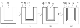
- FIG. 2 shows a schematic cross-sectional view for explaining the formation process of the wiring structure 20 in the conventional semiconductor device.
- a wiring groove 22 is formed in the insulating layer 21.
- a diffusion barrier layer 23 such as TaN is formed on the inner surface of the wiring groove 22.
- a liner layer 24 such as Ta or Co is formed on the diffusion barrier layer 23.
- Copper wiring 25 is embedded on the liner layer 24.
- the embedding of the copper wiring 25 includes, for example, a step of forming a copper seed layer on the liner layer and a subsequent step of electrolytic copper plating.
- the occupied portion of the copper wiring 25 becomes narrow. That is, the volume ratio of the copper wiring 25 filled in the wiring groove 22 becomes small.
- the degree of increase in wiring resistance due to miniaturization cannot be overlooked even with a slight decrease in volume ratio. Therefore, in order to cope with the miniaturization of the technical node of the LSI, it is desirable to provide a wiring structure capable of increasing the volume ratio of the copper wiring filled in the wiring groove 22.
- the present invention has been created in view of the above circumstances, and in one embodiment, it has a diffusion barrier layer having both a diffusion barrier function and a liner function, instead of forming two individual diffusion barrier layers and a liner layer.
- An object of the present invention is to provide a semiconductor device having a wiring structure.
- the inventor of the present invention has diligently studied to solve the above problems, and found that a diffusion barrier layer having both a diffusion barrier function and a liner function can be obtained by combining specific elements.
- the present invention completed based on the above findings is exemplified below.
- a semiconductor device having a wiring structure having an insulating layer, a conductive wiring, and a diffusion barrier layer arranged in contact with both the insulating layer and the conductive wiring between the insulating layer and the conductive wiring.
- the insulating layer contains a silicon oxide and / or a silicon oxide containing at least one element of C, N and H.
- Conductive wiring contains Cu and / or Co and
- the diffusion barrier layer is composed of an alloy having an amorphous structure containing a total of 90% by mass or more of the first metal and the second element.
- the first metal is any one selected from Co, Ru, and Mo.
- the second element is one or more selected from Zr, Al and Nb.
- the first metal is Ru
- the second element is Zr
- the first metal is Mo
- the second element is one or two selected from Y and B, Semiconductor device.
- the semiconductor device has a wiring structure having a diffusion barrier layer having both a diffusion barrier function and a liner function.
- the wiring structure it is not necessary to form two separate diffusion barrier layers and a liner layer, and it is sufficient to form a single diffusion barrier layer. Therefore, it occupies conductive wiring such as copper filled in the wiring groove. It is possible to increase the volume ratio of the parts, and for example, it is possible to obtain a special effect that the degree of increase in wiring resistance due to miniaturization of LSI can be alleviated.
- FIG. 1A shows a schematic cross-sectional view for explaining the wiring structure 10 included in the semiconductor device according to the embodiment of the present invention.
- the wiring structure 10 is a diffusion barrier layer 13 disposed between the insulating layer 11, the conductive wiring 15, and the insulating layer 11 and the conductive wiring 15 in contact with both the insulating layer 11 and the conductive wiring 15. And have.
- the insulating layer contains a silicon oxide and / or a silicon oxide containing at least one element of C, N and H.
- the insulating layer may contain a total of 90% by mass or more of silicon oxide and / or a silicon oxide containing at least one element of C, N and H, and 95% by mass or more. It may be contained in 99% by mass or more.
- Specific examples of these silicon oxides constituting the insulating layer are, but are not limited, silicon dioxide (SiO 2 ), silicon oxycarbide (SiO x Cy ), and silicon hydride oxycarbide (SiO x Cy H).
- z silicon oxynitride
- SiO x N y silicon oxynitride
- the conductive wiring contains Cu and / or Co in one embodiment.
- the conductive wiring may contain Cu and / or Co in a total amount of 50% by mass or more, 90% by mass or more, or 99% by mass or more.
- the conductive wiring may contain 90% by mass or more of Cu or 99% by mass or more of Cu.
- the conductive wiring may contain 90% by mass or more of Co or 99% by mass or more.
- the diffusion barrier layer is composed of an alloy having an amorphous structure containing a total of 90% by mass or more of the first metal and the second element. In another embodiment, the diffusion barrier layer is composed of an alloy having an amorphous structure containing a total of 95% by mass or more of the first metal and the second element. In yet another embodiment, the diffusion barrier layer is composed of an alloy having an amorphous structure containing a total of 99% by mass or more of the first metal and the second element.
- the diffusion barrier layer does not have to contain elements other than the first metal and the second element, but may contain intentional additive elements in addition to unavoidable impurities.
- the intentional additive element includes, but is not limited to, Group 15 elements such as nitrogen and phosphorus. The intentional additive element may be added alone or in combination of two or more.
- any one selected from Co, Ru, and Mo can be selected. These metals have low electrical resistivity and are also excellent in wettability and adhesion to Cu and / or Co, which are constituent materials of conductive wiring. This is advantageous in exerting the liner function.
- Co, Ru, and Mo tend to have a polycrystalline structure, and it is not possible to prevent Cu and / or Co, which are constituent materials of the conductive wiring, from diffusing into the insulating layer along the crystal grain boundaries. Further, there is a problem that these metals do not have sufficient adhesion to the insulating layer.
- the present inventor got the idea of combining the first metal with an appropriate second element so that the amorphous structure can exist stably. If an amorphous structure having no grain boundaries can be stably present, the above diffusion can be effectively suppressed, and the diffusion barrier function and the liner function can be exhibited at the same time. Further, by selecting an element having a strong tendency to form an oxide as the second element, that is, an element having a large negative value in the oxide standard formation Gibbs energy, the adhesion to the insulating layer can be ensured.
- the second element is preferably one or more selected from Zr, Al and Nb.
- the atomic ratio of Co and Zr in the Co—Zr alloy satisfies 0.1 ⁇ Zr / (Co + Zr) ⁇ 0.8.
- the atomic ratio of Co and Al in the Co—Al alloy satisfies 0.4 ⁇ Al / (Co + Al) ⁇ 0.9.
- the atomic ratio of Co and Nb in the Co—Nb alloy satisfies 0.4 ⁇ Nb / (Co + Nb) ⁇ 0.9. It is more preferable to satisfy 0.5 ⁇ Nb / (Co + Nb) ⁇ 0.8 from the viewpoint that the diffusion barrier function and the adhesion can be satisfactorily secured.
- the second element is preferably Zr.
- the atomic ratio of Ru and Zr in the Ru—Zr alloy satisfies 0.1 ⁇ Zr / (Ru + Zr) ⁇ 0.8.
- the second element is preferably one or two selected from Y and B.
- the atomic ratio of Mo and Y in the Mo—Y alloy satisfies 0.5 ⁇ Y / (Mo + Y) ⁇ 0.9.
- the atomic ratio of Mo and B in the Mo-B alloy satisfies 0.2 ⁇ B / (Mo + B) ⁇ 0.8.
- the atomic ratio of Mo, Y and B in the Mo-Y-B alloy is 0.5 ⁇ (Y + B) / ( It is preferable to satisfy Mo + Y + B) ⁇ 0.9, and it is more preferable to satisfy 0.6 ⁇ (Y + B) / (Mo + Y + B) ⁇ 0.8 from the viewpoint of ensuring good diffusion barrier function and adhesion. ..
- An alloy having an amorphous structure containing a total of 90% by mass or more of the first metal and the second element has a second atomic concentration of the first metal from the viewpoint of achieving both a diffusion barrier function and a liner function. It is preferably equal to or higher than the atomic concentration of the element.
- the thickness of the diffusion barrier layer can be 5 nm or less, 3 nm or less, and for example, 1 nm to 5 nm in one embodiment. ..
- the thickness and composition of the diffusion barrier layer are determined by the following procedure. For example, a case where an alloy thin film is formed by simultaneously sputtering a diffusion barrier layer composed of a first metal and a second element and forming a simple substance of each element will be described. First, only the first metal is sputter-deposited, and the film-forming rate is determined by measuring the relationship between the film-forming time and the film thickness. The film thickness can be measured using a stylus type film thickness meter. Next, only the second element is sputtered into a film to determine the film formation rate. Based on these film forming speeds, the film forming conditions are adjusted to obtain an alloy thin film having a desired composition.
- composition of the obtained alloy thin film is measured using a fluorescent X-ray analyzer (XRF), and it is confirmed that the desired composition and the actual composition are obtained with an error of within ⁇ 0.1 atomic%.
- XRF fluorescent X-ray analyzer
- a cross section of a sample having a laminated structure of conductive wiring / diffusion barrier layer / insulating layer / silicon substrate is observed with a scanning transmission electron microscope (STEM), and the thickness direction of the laminated structure is observed. Elemental analysis (STEM-EDS analysis) by EDS (energy dispersive X-ray spectroscope) of the constituent elements is performed, and a characteristic X-ray intensity profile showing the energy peculiar to each constituent element is obtained.
- the atomic concentration profile of the constituent elements of each layer can be qualitatively known. This information is useful for investigating the presence or absence of mutual diffusion between layers during high temperature heat treatment.
- the measurement conditions for STEM-EDS analysis are an acceleration voltage of 200 kV, an observation magnification of 500,000 times, and a beam diameter of 0.2 nm. Since the intensity profile tends to be broad as the beam diameter becomes large, it is desirable to set the beam diameter to a constant value of 1 nm or less in order to perform reproducible measurement.
- the semiconductor device to which the present invention is applicable is not particularly limited as long as it has at least a part of the wiring structure according to the above-described embodiment.
- Examples of the semiconductor device include semiconductor integrated circuits having multi-layer wiring (typically, wiring of 10 layers or more) such as LSI.
- it is suitable for a semiconductor device having a wiring structure of 25 nm or less, preferably 15 nm or less, which is a wiring width at a level where the degree of increase in wiring resistance due to miniaturization cannot be overlooked even if the volume ratio of wiring is slightly reduced. Applicable.
- the wiring structure according to an embodiment of the present invention is a lowermost layer formed in a MOL (Middle of Line) step following a FEOL (Front End of Line) step of forming a transistor on a semiconductor substrate in a semiconductor integrated circuit. It is applicable to the wiring structure of.
- the wiring structure according to another embodiment of the present invention can be applied to the wiring structure of the metal layer formed in the BOOL (Back End of Line) process after the MOL process in the semiconductor integrated circuit.
- the wiring groove 12 is formed in the insulating layer 11.
- the insulating layer 11 may form an insulating film between wirings.
- the insulating layer 11 may form an interlayer insulating film.
- the insulating layer 11 can be formed by a coating method such as a spin coating method or a spray method in addition to the chemical vapor deposition method (CVD).
- the formation of the wiring groove 12 can be carried out by a known lithography and etching technique.
- the wiring groove 12 may be further provided with a contact hole and a beer hole.
- the wiring groove shall include the concepts of contact holes and beer holes.
- the diffusion barrier layer 13 is formed on the inner surface of the wiring groove 12.
- the diffusion barrier layer 13 can be formed by, for example, a sputtering method, a CVD method, or an atomic layer deposition method (ALD).
- the wiring groove 12 after forming the diffusion barrier layer 13 is embedded with the conductive wiring 15.
- the embedding of the conductive wiring 15 includes, for example, a step of forming a seed layer on the barrier layer and a subsequent electrolytic plating step.
- the composition of the obtained Co—Zr alloy film having a planar shape was measured by irradiating the film surface with X-rays using XRF.
- the cross-sectional material thinned by a focused ion beam device (FIB) is taken out from the obtained laminate by microsampling, and the alloy film portion of the laminate is diffracted with STEM (JEOL, model JEM-2100F).
- STEM JEOL, model JEM-2100F
- the adhesion between the Co—Zr alloy film (Co—Zr diffusion barrier layer) and the SiO 2 film in the laminate obtained in the above test was evaluated according to ASTM D3359-97 (tape test). Specifically, 11 ⁇ 11 cuts are made in a grid pattern at intervals of 1 mm in the Co—Zr alloy film of each test example, and then a cellophane adhesive tape having an adhesive strength of 4 N / cm is attached to the tape. The state of the peeled portion of the Co—Zr alloy film at the time of peeling was evaluated on a scale of 0 to 5 according to ASTM D3359-97. The higher the adhesion, the larger the evaluation value.
- the tape test was performed separately at room temperature (25 ° C.), after heat treatment at 260 ° C. ⁇ 10 minutes to cool to room temperature, and after heat treatment at 400 ° C. ⁇ 10 minutes to cool to room temperature. .. From these results, A is the case where the evaluation in ASTM D3359-97 is 5 under any temperature condition, B is the case where the evaluation is 3 to 4 under any temperature condition, and the evaluation is based on any temperature condition. The case of 2 or less was evaluated as C for Co—Zr alloy films having various compositions. The results are shown in Table 1.
- a silicon wafer with a SiO 2 film with a thickness of 20 nm is charged into a magnetron sputtering device capable of simultaneously sputtering a Co target and a Zr target in the same chamber, and a Co—Zr alloy film with a thickness of 3 nm is placed on the SiO 2 film.
- the composition of the Co—Zr alloy film was changed by changing the input power of each sputtered cathode. Further, a Cu thin film having a thickness of 150 nm was formed on the Co—Zr alloy film.
- the thicknesses of the SiO 2 film, the Co—Zr alloy film, and the Cu thin film were calculated based on the film formation rate determined in advance by measuring the relationship between the film formation time and the film thickness, respectively.
- a stylus type film thickness meter (Made by Bruker, model DektakXT) was used.
- the adhesion between the Cu thin film and the Co—Zr alloy film in the laminate obtained in the above test was evaluated according to ASTM D3359-97 (tape test).
- the tape test was performed separately at room temperature (25 ° C.), after heat treatment at 260 ° C. ⁇ 10 minutes to cool to room temperature, and after heat treatment at 400 ° C. ⁇ 10 minutes to cool to room temperature. .. From these results, A is the case where the evaluation in ASTM D3359-97 is 5 under any temperature condition, B is the case where the evaluation is 3 to 4 under any temperature condition, and evaluation is made under any temperature condition. The case where was 2 or less was evaluated as C for various compositions. The results are shown in Table 1.
- the sample used for the evaluation was prepared as follows. A SiO 2 layer having a thickness of 20 nm was formed on a p-type silicon wafer, a resist film was formed on the layer, and an electrode-shaped hole was formed in the resist film by photolithography. On this, a Co—Zr alloy film having a thickness of 3 nm and a Cu film having a thickness of 150 nm were formed. Then, the resist film was peeled off with acetone. At this time, Cu / Co—Zr formed in the hole portion of the resist film remains on the wafer and functions as an electrode. Further, a 400 nm aluminum electrode was produced on the back surface of the wafer by sputtering.
- the obtained laminate was pre-annealed in an atmosphere of Ar + 5% by volume H 2 at 300 ° C. for 30 minutes, then CV (Capacitance-Voltage) measurement was performed, and the flat band voltage (V FB ) was measured. This V FB was used as the initial value. Then, while heating the laminate to 250 ° C. in an atmosphere of Ar + 5% by volume H 2 , a BTS (Bias Temperature Stress) is applied for 45 minutes between both electrodes with Cu as the positive electrode and Al as the negative electrode. ) was given. After that, CV measurement was performed and V FB was measured.
- CV Capacitance-Voltage
- V FB (BTS) after the BTS test and V FB (initial) in the initial state is obtained, and when V FB (BTS) -V FB (initial) ⁇ -0.3 V is satisfied, it has a diffusion barrier function. evaluated. Y was given when the criteria were met, and N was given when the criteria were not met. The results are shown in Table 1.
- the diffusion barrier layer is replaced with a Co—Al alloy, a Co—Nb alloy, a Ru—Zr alloy, a Mo—Y alloy, and a Mo—B alloy, and the same structural evaluation and adhesion evaluation as described above are used. , And barrier properties were evaluated. The results are shown in Tables 2 to 6, respectively.
- the following points were confirmed.
- the Co—Zr alloy it is preferable to satisfy 0.1 ⁇ Zr / (Co + Zr) ⁇ 0.8, and more preferably 0.15 ⁇ Zr / (Co + Zr) ⁇ 0.5.
- the Co—Al alloy it is preferable to satisfy 0.4 ⁇ Al / (Co + Al) ⁇ 0.9, and more preferably 0.5 ⁇ Al / (Co + Al) ⁇ 0.8.
- the Co—Nb alloy it is preferable to satisfy 0.4 ⁇ Nb / (Co + Nb) ⁇ 0.9, and more preferably 0.5 ⁇ Nb / (Co + Nb) ⁇ 0.8.
- Ru—Zr alloy it is preferable to satisfy 0.1 ⁇ Zr / (Ru + Zr) ⁇ 0.8, and more preferably 0.3 ⁇ Zr / (Ru + Zr) ⁇ 0.6.
- Mo—Y alloy it is preferable to satisfy 0.5 ⁇ Y / (Mo + Y) ⁇ 0.9, and more preferably 0.6 ⁇ Y / (Mo + Y) ⁇ 0.8.
- Mo-B alloy it is preferable to satisfy 0.2 ⁇ B / (Mo + B) ⁇ 0.8, and more preferably 0.3 ⁇ B / (Mo + B) ⁇ 0.7.
- Wiring structure 11 Insulation layer 12 Wiring groove 13 Diffusion barrier layer 15 Conductive wiring 20 Wiring structure 21 Insulation layer 22 Wiring groove 23 Diffusion barrier layer 24 Liner layer 25 Copper wiring 30 Laminated body 31 p-type silicon wafer 32 SiO 2 film 33 Co -Zr alloy film
Landscapes
- Internal Circuitry In Semiconductor Integrated Circuit Devices (AREA)
- Electrodes Of Semiconductors (AREA)
- Crystals, And After-Treatments Of Crystals (AREA)
Priority Applications (6)
| Application Number | Priority Date | Filing Date | Title |
|---|---|---|---|
| CN202080101478.7A CN115699268A (zh) | 2020-06-04 | 2020-06-04 | 半导体器件 |
| JP2022528359A JP7525186B2 (ja) | 2020-06-04 | 2020-06-04 | 半導体デバイス |
| KR1020227043096A KR102865111B1 (ko) | 2020-06-04 | 2020-06-04 | 반도체 디바이스 |
| PCT/JP2020/022202 WO2021245893A1 (ja) | 2020-06-04 | 2020-06-04 | 半導体デバイス |
| US17/928,428 US12444686B2 (en) | 2020-06-04 | 2020-06-04 | Semiconductor device |
| TW110118925A TWI795789B (zh) | 2020-06-04 | 2021-05-25 | 半導體設備 |
Applications Claiming Priority (1)
| Application Number | Priority Date | Filing Date | Title |
|---|---|---|---|
| PCT/JP2020/022202 WO2021245893A1 (ja) | 2020-06-04 | 2020-06-04 | 半導体デバイス |
Publications (1)
| Publication Number | Publication Date |
|---|---|
| WO2021245893A1 true WO2021245893A1 (ja) | 2021-12-09 |
Family
ID=78830718
Family Applications (1)
| Application Number | Title | Priority Date | Filing Date |
|---|---|---|---|
| PCT/JP2020/022202 Ceased WO2021245893A1 (ja) | 2020-06-04 | 2020-06-04 | 半導体デバイス |
Country Status (6)
| Country | Link |
|---|---|
| US (1) | US12444686B2 (https=) |
| JP (1) | JP7525186B2 (https=) |
| KR (1) | KR102865111B1 (https=) |
| CN (1) | CN115699268A (https=) |
| TW (1) | TWI795789B (https=) |
| WO (1) | WO2021245893A1 (https=) |
Citations (5)
| Publication number | Priority date | Publication date | Assignee | Title |
|---|---|---|---|---|
| JPH11145141A (ja) * | 1997-11-14 | 1999-05-28 | Matsushita Electron Corp | 半導体装置 |
| JP2001007204A (ja) * | 1999-06-24 | 2001-01-12 | Nec Corp | 多層配線の構造及びその製造方法 |
| JP2008053753A (ja) * | 2007-11-08 | 2008-03-06 | Toshiba Corp | 半導体装置の製造方法 |
| JP2008098424A (ja) * | 2006-10-12 | 2008-04-24 | Rohm Co Ltd | 半導体装置および半導体装置の製造方法 |
| JP2012169480A (ja) * | 2011-02-15 | 2012-09-06 | Panasonic Corp | 半導体装置及びその製造方法 |
Family Cites Families (12)
| Publication number | Priority date | Publication date | Assignee | Title |
|---|---|---|---|---|
| US8696875B2 (en) | 1999-10-08 | 2014-04-15 | Applied Materials, Inc. | Self-ionized and inductively-coupled plasma for sputtering and resputtering |
| US6833058B1 (en) * | 2000-10-24 | 2004-12-21 | Honeywell International Inc. | Titanium-based and zirconium-based mixed materials and sputtering targets |
| CN101847598B (zh) | 2001-11-14 | 2012-06-20 | 应用材料有限公司 | 用于溅射和再溅射的自离子化及电感耦合等离子体 |
| JP4591084B2 (ja) | 2002-12-09 | 2010-12-01 | 日本電気株式会社 | 配線用銅合金、半導体装置及び半導体装置の製造方法 |
| CN1957487A (zh) * | 2004-01-06 | 2007-05-02 | Cymbet公司 | 具有一个或者更多个可限定层的层式阻挡物结构和方法 |
| KR100761467B1 (ko) * | 2006-06-28 | 2007-09-27 | 삼성전자주식회사 | 금속배선 및 그 형성 방법 |
| US9735123B2 (en) * | 2014-03-13 | 2017-08-15 | Taiwan Semiconductor Manufacturing Company, Ltd. | Semiconductor device structure and manufacturing method |
| KR102662612B1 (ko) | 2016-10-02 | 2024-05-03 | 어플라이드 머티어리얼스, 인코포레이티드 | 루테늄 라이너로 구리 전자 이동을 개선하기 위한 도핑된 선택적 금속 캡 |
| US10510657B2 (en) * | 2017-09-26 | 2019-12-17 | Taiwan Semiconductor Manufacturing Co., Ltd. | Semiconductor device with interconnecting structure and method for manufacturing the same |
| US10796995B2 (en) | 2017-11-29 | 2020-10-06 | Tohoku University | Semiconductor devices including a first cobalt alloy in a first barrier layer and a second cobalt alloy in a second barrier layer |
| US11043373B2 (en) * | 2018-07-31 | 2021-06-22 | Taiwan Semiconductor Manufacturing Company, Ltd. | Interconnect system with improved low-k dielectrics |
| US11158538B2 (en) * | 2020-02-04 | 2021-10-26 | International Business Machines Corporation | Interconnect structures with cobalt-infused ruthenium liner and a cobalt cap |
-
2020
- 2020-06-04 JP JP2022528359A patent/JP7525186B2/ja active Active
- 2020-06-04 KR KR1020227043096A patent/KR102865111B1/ko active Active
- 2020-06-04 WO PCT/JP2020/022202 patent/WO2021245893A1/ja not_active Ceased
- 2020-06-04 US US17/928,428 patent/US12444686B2/en active Active
- 2020-06-04 CN CN202080101478.7A patent/CN115699268A/zh active Pending
-
2021
- 2021-05-25 TW TW110118925A patent/TWI795789B/zh active
Patent Citations (5)
| Publication number | Priority date | Publication date | Assignee | Title |
|---|---|---|---|---|
| JPH11145141A (ja) * | 1997-11-14 | 1999-05-28 | Matsushita Electron Corp | 半導体装置 |
| JP2001007204A (ja) * | 1999-06-24 | 2001-01-12 | Nec Corp | 多層配線の構造及びその製造方法 |
| JP2008098424A (ja) * | 2006-10-12 | 2008-04-24 | Rohm Co Ltd | 半導体装置および半導体装置の製造方法 |
| JP2008053753A (ja) * | 2007-11-08 | 2008-03-06 | Toshiba Corp | 半導体装置の製造方法 |
| JP2012169480A (ja) * | 2011-02-15 | 2012-09-06 | Panasonic Corp | 半導体装置及びその製造方法 |
Also Published As
| Publication number | Publication date |
|---|---|
| TW202147938A (zh) | 2021-12-16 |
| US20230154851A1 (en) | 2023-05-18 |
| KR20230020995A (ko) | 2023-02-13 |
| JP7525186B2 (ja) | 2024-07-30 |
| US12444686B2 (en) | 2025-10-14 |
| TWI795789B (zh) | 2023-03-11 |
| CN115699268A (zh) | 2023-02-03 |
| JPWO2021245893A1 (https=) | 2021-12-09 |
| KR102865111B1 (ko) | 2025-09-25 |
Similar Documents
| Publication | Publication Date | Title |
|---|---|---|
| US5622608A (en) | Process of making oxidation resistant high conductivity copper layers | |
| JP2000049116A (ja) | 半導体装置及びその製造方法 | |
| JPH1098011A (ja) | 半導体装置及びその製造方法 | |
| US20090120787A1 (en) | Method of manufacturing semiconductor device | |
| US11840756B2 (en) | Binary Ag—Cu amorphous thin-films for electronic applications | |
| KR101045831B1 (ko) | 반도체 장치 및 그 제조 방법 | |
| An et al. | Amorphous Ta x Mn y O z layer as a diffusion barrier for advanced copper interconnects | |
| Joi et al. | Doped Ru to enable next generation barrier-less interconnect | |
| KR20030020986A (ko) | 스퍼터링 타겟 | |
| JP3315211B2 (ja) | 電子部品 | |
| US20050156315A1 (en) | Thin films, structures having thin films, and methods of forming thin films | |
| Murarka et al. | Copper interconnection schemes: elimination of the need of diffusion barrier/adhesion promoter by the use of corrosion-resistant low-resistivity-doped copper | |
| Wojcik et al. | Characterization of Ru–Mn composites for ULSI interconnects | |
| KR100365061B1 (ko) | 반도체소자및반도체소자제조방법 | |
| WO2021245893A1 (ja) | 半導体デバイス | |
| Brückner et al. | Resistance behaviour and interdiffusion of layered CuNi-NiCr films | |
| JP5194549B2 (ja) | 半導体装置の製造方法 | |
| JP2024057514A (ja) | 不揮発性スイッチング素子の製造方法 | |
| Koike et al. | Self‐Formed Barrier with Cu‐Mn alloy Metallization and its Effects on Reliability | |
| US20250157932A1 (en) | Low resistance liner | |
| Hayashi et al. | Low Resistive Ru Thin Film on Dielectrics without Adhesive Liner for Sub-2nm Interconnects | |
| JP5569561B2 (ja) | 半導体装置の製造方法 | |
| JP2010185139A (ja) | Cu合金膜および表示デバイス | |
| JP2004289174A (ja) | 半導体装置及びその製造方法 | |
| JP5817856B2 (ja) | 半導体装置 |
Legal Events
| Date | Code | Title | Description |
|---|---|---|---|
| 121 | Ep: the epo has been informed by wipo that ep was designated in this application |
Ref document number: 20939381 Country of ref document: EP Kind code of ref document: A1 |
|
| ENP | Entry into the national phase |
Ref document number: 2022528359 Country of ref document: JP Kind code of ref document: A |
|
| NENP | Non-entry into the national phase |
Ref country code: DE |
|
| 122 | Ep: pct application non-entry in european phase |
Ref document number: 20939381 Country of ref document: EP Kind code of ref document: A1 |
|
| WWG | Wipo information: grant in national office |
Ref document number: 17928428 Country of ref document: US |