WO2021234923A1 - 電力変換装置、電力変換制御装置、及び制御方法 - Google Patents
電力変換装置、電力変換制御装置、及び制御方法 Download PDFInfo
- Publication number
- WO2021234923A1 WO2021234923A1 PCT/JP2020/020172 JP2020020172W WO2021234923A1 WO 2021234923 A1 WO2021234923 A1 WO 2021234923A1 JP 2020020172 W JP2020020172 W JP 2020020172W WO 2021234923 A1 WO2021234923 A1 WO 2021234923A1
- Authority
- WO
- WIPO (PCT)
- Prior art keywords
- control
- control deviation
- converter
- result
- arithmetic processing
- Prior art date
- Legal status (The legal status is an assumption and is not a legal conclusion. Google has not performed a legal analysis and makes no representation as to the accuracy of the status listed.)
- Ceased
Links
Images




Classifications
-
- H—ELECTRICITY
- H02—GENERATION; CONVERSION OR DISTRIBUTION OF ELECTRIC POWER
- H02M—APPARATUS FOR CONVERSION BETWEEN AC AND AC, BETWEEN AC AND DC, OR BETWEEN DC AND DC, AND FOR USE WITH MAINS OR SIMILAR POWER SUPPLY SYSTEMS; CONVERSION OF DC OR AC INPUT POWER INTO SURGE OUTPUT POWER; CONTROL OR REGULATION THEREOF
- H02M7/00—Conversion of AC power input into DC power output; Conversion of DC power input into AC power output
- H02M7/02—Conversion of AC power input into DC power output without possibility of reversal
- H02M7/04—Conversion of AC power input into DC power output without possibility of reversal by static converters
- H02M7/12—Conversion of AC power input into DC power output without possibility of reversal by static converters using discharge tubes with control electrode or semiconductor devices with control electrode
- H02M7/21—Conversion of AC power input into DC power output without possibility of reversal by static converters using discharge tubes with control electrode or semiconductor devices with control electrode using devices of a triode or transistor type requiring continuous application of a control signal
- H02M7/217—Conversion of AC power input into DC power output without possibility of reversal by static converters using discharge tubes with control electrode or semiconductor devices with control electrode using devices of a triode or transistor type requiring continuous application of a control signal using semiconductor devices only
- H02M7/219—Conversion of AC power input into DC power output without possibility of reversal by static converters using discharge tubes with control electrode or semiconductor devices with control electrode using devices of a triode or transistor type requiring continuous application of a control signal using semiconductor devices only in a bridge configuration
-
- H—ELECTRICITY
- H02—GENERATION; CONVERSION OR DISTRIBUTION OF ELECTRIC POWER
- H02M—APPARATUS FOR CONVERSION BETWEEN AC AND AC, BETWEEN AC AND DC, OR BETWEEN DC AND DC, AND FOR USE WITH MAINS OR SIMILAR POWER SUPPLY SYSTEMS; CONVERSION OF DC OR AC INPUT POWER INTO SURGE OUTPUT POWER; CONTROL OR REGULATION THEREOF
- H02M5/00—Conversion of AC power input into AC power output, e.g. for change of voltage, for change of frequency, for change of number of phases
- H02M5/40—Conversion of AC power input into AC power output, e.g. for change of voltage, for change of frequency, for change of number of phases with intermediate conversion into DC
- H02M5/42—Conversion of AC power input into AC power output, e.g. for change of voltage, for change of frequency, for change of number of phases with intermediate conversion into DC by static converters
- H02M5/44—Conversion of AC power input into AC power output, e.g. for change of voltage, for change of frequency, for change of number of phases with intermediate conversion into DC by static converters using discharge tubes or semiconductor devices to convert the intermediate DC into AC
- H02M5/453—Conversion of AC power input into AC power output, e.g. for change of voltage, for change of frequency, for change of number of phases with intermediate conversion into DC by static converters using discharge tubes or semiconductor devices to convert the intermediate DC into AC using devices of a triode or transistor type requiring continuous application of a control signal
- H02M5/458—Conversion of AC power input into AC power output, e.g. for change of voltage, for change of frequency, for change of number of phases with intermediate conversion into DC by static converters using discharge tubes or semiconductor devices to convert the intermediate DC into AC using devices of a triode or transistor type requiring continuous application of a control signal using semiconductor devices only
-
- H—ELECTRICITY
- H02—GENERATION; CONVERSION OR DISTRIBUTION OF ELECTRIC POWER
- H02P—CONTROL OR REGULATION OF ELECTRIC MOTORS, ELECTRIC GENERATORS OR DYNAMO-ELECTRIC CONVERTERS; CONTROLLING TRANSFORMERS, REACTORS OR CHOKE COILS
- H02P23/00—Arrangements or methods for the control of AC motors characterised by a control method other than vector control
-
- H—ELECTRICITY
- H02—GENERATION; CONVERSION OR DISTRIBUTION OF ELECTRIC POWER
- H02M—APPARATUS FOR CONVERSION BETWEEN AC AND AC, BETWEEN AC AND DC, OR BETWEEN DC AND DC, AND FOR USE WITH MAINS OR SIMILAR POWER SUPPLY SYSTEMS; CONVERSION OF DC OR AC INPUT POWER INTO SURGE OUTPUT POWER; CONTROL OR REGULATION THEREOF
- H02M1/00—Details of apparatus for conversion
- H02M1/0003—Details of control, feedback or regulation circuits
- H02M1/0025—Arrangements for modifying reference values, feedback values or error values in the control loop of a converter
-
- H—ELECTRICITY
- H02—GENERATION; CONVERSION OR DISTRIBUTION OF ELECTRIC POWER
- H02P—CONTROL OR REGULATION OF ELECTRIC MOTORS, ELECTRIC GENERATORS OR DYNAMO-ELECTRIC CONVERTERS; CONTROLLING TRANSFORMERS, REACTORS OR CHOKE COILS
- H02P27/00—Arrangements or methods for the control of AC motors characterised by the kind of supply voltage
- H02P27/04—Arrangements or methods for the control of AC motors characterised by the kind of supply voltage using variable-frequency supply voltage, e.g. inverter or converter supply voltage
- H02P27/06—Arrangements or methods for the control of AC motors characterised by the kind of supply voltage using variable-frequency supply voltage, e.g. inverter or converter supply voltage using DC to AC converters or inverters
-
- H—ELECTRICITY
- H02—GENERATION; CONVERSION OR DISTRIBUTION OF ELECTRIC POWER
- H02P—CONTROL OR REGULATION OF ELECTRIC MOTORS, ELECTRIC GENERATORS OR DYNAMO-ELECTRIC CONVERTERS; CONTROLLING TRANSFORMERS, REACTORS OR CHOKE COILS
- H02P29/00—Arrangements for regulating or controlling electric motors, appropriate for both AC and DC motors
- H02P29/40—Regulating or controlling the amount of current drawn or delivered by the motor for controlling the mechanical load
-
- H—ELECTRICITY
- H02—GENERATION; CONVERSION OR DISTRIBUTION OF ELECTRIC POWER
- H02M—APPARATUS FOR CONVERSION BETWEEN AC AND AC, BETWEEN AC AND DC, OR BETWEEN DC AND DC, AND FOR USE WITH MAINS OR SIMILAR POWER SUPPLY SYSTEMS; CONVERSION OF DC OR AC INPUT POWER INTO SURGE OUTPUT POWER; CONTROL OR REGULATION THEREOF
- H02M5/00—Conversion of AC power input into AC power output, e.g. for change of voltage, for change of frequency, for change of number of phases
- H02M5/40—Conversion of AC power input into AC power output, e.g. for change of voltage, for change of frequency, for change of number of phases with intermediate conversion into DC
- H02M5/42—Conversion of AC power input into AC power output, e.g. for change of voltage, for change of frequency, for change of number of phases with intermediate conversion into DC by static converters
- H02M5/44—Conversion of AC power input into AC power output, e.g. for change of voltage, for change of frequency, for change of number of phases with intermediate conversion into DC by static converters using discharge tubes or semiconductor devices to convert the intermediate DC into AC
- H02M5/453—Conversion of AC power input into AC power output, e.g. for change of voltage, for change of frequency, for change of number of phases with intermediate conversion into DC by static converters using discharge tubes or semiconductor devices to convert the intermediate DC into AC using devices of a triode or transistor type requiring continuous application of a control signal
- H02M5/458—Conversion of AC power input into AC power output, e.g. for change of voltage, for change of frequency, for change of number of phases with intermediate conversion into DC by static converters using discharge tubes or semiconductor devices to convert the intermediate DC into AC using devices of a triode or transistor type requiring continuous application of a control signal using semiconductor devices only
- H02M5/4585—Conversion of AC power input into AC power output, e.g. for change of voltage, for change of frequency, for change of number of phases with intermediate conversion into DC by static converters using discharge tubes or semiconductor devices to convert the intermediate DC into AC using devices of a triode or transistor type requiring continuous application of a control signal using semiconductor devices only having a rectifier with controlled elements
Definitions
- the present invention relates to a power conversion device, a power conversion control device, and a control method.
- Some power converters are equipped with a converter and an inverter in their main circuit.
- a power conversion device converts the power relayed via the DC section provided between the converter and the inverter.
- the voltage in this DC section is adjusted by controlling the converter. If the load of the inverter fluctuates relatively large during the operation of the power conversion device, the voltage in this DC section may fluctuate relatively large due to this.
- the power conversion device of the embodiment includes a converter, an inverter, and a control unit.
- the converter converts the electric power supplied from the power supply side into DC electric power.
- the inverter is provided on the output side of the converter.
- the control unit uses the DC voltage of the DC section provided on the output side of the converter as the feedback amount to calculate the control deviation between the target amount and the feedback amount with respect to the control target voltage of the DC section.
- a non-linear arithmetic processing is performed on the control deviation, an operation amount based on the result of the non-linear arithmetic processing is calculated, and the converter is controlled using the operation amount.
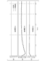
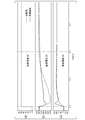
- the block diagram of the power conversion apparatus of 1st Embodiment The figure for demonstrating the analysis result of the voltage control of 1st Embodiment. The figure for demonstrating the analysis result of the voltage control of 1st Embodiment. The figure for demonstrating the analysis result of the voltage control of 1st Embodiment.
- the block diagram of the power conversion apparatus of the 2nd Embodiment The figure for demonstrating the nonlinear arithmetic processing of 2nd Embodiment.
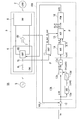
- FIG. 1 is a block diagram of the power conversion device 1 of the first embodiment.
- the power conversion device 1 includes, for example, a main circuit 3 that supplies power to a load 2 (the description in the figure is LOAD), a voltage sensor 9V, a current sensor 9i, and a control unit 10. Three-phase AC power is shared from the power supply 5 to the input side of the main circuit 3.
- the main circuit 3 includes a converter 6 (the description in the figure is CNV), a capacitor 7, and an inverter 8 (the description in the figure is INV).
- the converter 6 converts the power supplied from the power supply 5 side into DC power.
- a DC section is provided on the output side of the converter 6.
- a smoothing capacitor 7 and an input of the inverter 8 are connected in parallel to the output of the converter 6 via a DC section.
- the capacitor 7 may be provided independently of the converter 6 and the inverter 8, may be a part of the converter 6 or the inverter 8, or may be a combination thereof.
- the inverter 8 receives electric power from the converter 6 via the DC section.
- the main circuit 3 converts the electric power supplied via the DC section.
- the voltage sensor 9V detects the voltage in the DC section.
- the current sensor 9i detects the current flowing through the input of the converter 6.
- the converter 6 includes a reactor 6L and an IGBT 6S.
- the reactor 6L is provided in association with each phase of the three-phase alternating current.
- One end of the reactor 6L is connected to the input terminal of the converter 6 and is connected to the power supply 5 via the input terminal (not shown) of the converter 6.
- the other end of the reactor 6L is connected to the control terminal of the IGBT 6S.
- the IGBT 6S includes one or more semiconductor switches, and by turning on / off the semiconductor switch by a control signal supplied to the control terminal, the AC power supplied via the reactor 6L is converted into DC power.
- the control unit 10 calculates an operation amount based on the result of the nonlinear arithmetic processing, and controls the converter 6 using the operation amount. For example, the control unit 10 uses the voltage (DC voltage) in the DC section detected by the voltage sensor 9V as the feedback amount, and the control deviation between the target amount V * and the feedback amount VDC_F with respect to the control target voltage in the DC section. Is calculated, and the non-linear arithmetic processing for the control deviation is performed.
- the control unit 10 includes, for example, a current detection unit 11 (the description in the figure is IDET), a subtractor 12, a nonlinear calculation unit 13, a voltage control unit 14 (the description in the figure is AVR), and a current control unit 15. (The description in the figure is ACR) and the PWM control unit 16 (the description in the figure is PWM).
- the current detection unit 11 calculates the current detection values ID_det and IQ_det based on the detection value of the input current of the converter 6 detected by the current sensor 9i and the reference phase ⁇ . For example, the current detection unit 11 uses the reference phase ⁇ as the reference phase, and based on the detected value of the current of each of two or more phases of the three-phase alternating current on the input side of the converter 6, the stationary coordinate system of the UVW phase. Is converted into a rotating coordinate system including the D axis and the Q axis, and the current detection values ID_det and IQ_det are calculated.
- the reference phase ⁇ is a phase signal synchronized with the phase of the alternating current supplied to the converter 6, and is generated based on the phase of the alternating current by, for example, a phase detector (not shown).
- the subtractor 12 subtracts the feedback amount VDC_F from the voltage (DC voltage) in the DC section detected by the voltage sensor 9V from the target amount V * related to the control target voltage in the DC section designated by the host device, for example, to target the target.
- a control deviation ⁇ V0 between the quantity V * and the feedback quantity VDC_F is obtained.
- the nonlinear calculation unit 13 uses the control deviation ⁇ V0 regarding the target quantity V * and the feedback quantity VDC_F as an input variable, and performs a nonlinear calculation for the control deviation ⁇ V0 and a linear calculation of the magnification k according to a predetermined rule to perform a control deviation. Calculate k ⁇ V1.
- the nonlinear arithmetic unit 13 includes arithmetic units 13a, 13b, and 13c.
- the calculation unit 13a calculates the absolute value of the control deviation ⁇ V0.
- the arithmetic unit 13b is a multiplier, and the control deviation ⁇ V0 and the absolute value of the control deviation ⁇ V0 (
- the calculation unit 13c calculates the control deviation k ⁇ V1 by multiplying the control deviation ⁇ V1 by a coefficient k whose value is predetermined.
- the above arithmetic processing is organized into the following equations (1) and (2).
- the voltage control unit 14 calculates the current reference IQ_R having a value such that the control deviation k ⁇ V1 calculated by the nonlinear calculation unit 13 becomes 0. This corresponds to obtaining a current reference IQ_R having a value such that the control deviation ⁇ V1 is set to 0.
- the current reference IQ_R is a control target value that defines the magnitude of the effective current. It is preferable that the proportional element (P), the integrating element (I), and the differential element (D) are connected in parallel with each other.
- the voltage control unit 14 calculates the current reference IQ_R by PID calculation processing including the proportional element (P), the integrating element (I), and the differential element (D).
- the control deviation ⁇ V1 is commonly supplied to the inputs of the proportional element (P), the integrating element (I), and the differential element (D).
- the arithmetic processing by the voltage control unit 14 is not limited to the PID arithmetic processing.
- the arithmetic processing by the voltage control unit 14 is an arithmetic processing including at least one arithmetic element among the proportional element (P), the integral element (I), and the differential element (D) instead of the PID arithmetic processing. May be.
- the current control unit 15 is based on a current reference ID_R (not shown), a current reference IQ_R calculated by the voltage control unit 14, current detection values ID_det and IQ_det calculated by the current detection unit 11, and a reference phase ⁇ .
- the voltage reference EU_R, EV_R, and EW_R corresponding to each phase of alternating current are calculated.
- the current reference ID_R is a control target value that defines the magnitude of the reactive current, and may be, for example, a predetermined constant.
- the current control unit 15 calculates the voltage reference VD_R so that the deviation between the current reference ID_R and the current detection value ID_det becomes 0 for the D-axis component.
- the current control unit 15 calculates the voltage reference VD_R so that the deviation between the current reference IQ_R and the current detection value ID_det becomes 0 for the Q-axis component.
- the current control unit 15 uses the reference phase ⁇ based on the voltage reference VD_R of the D-axis component and the voltage reference VD_R of the Q-axis component from the rotating coordinate system including the D-axis and the Q-axis to the UVW phase. Convert to a stationary coordinate system that includes each axis.
- the PWM control unit 16 uses a carrier signal (not shown) based on the voltage reference EU_R, EV_R, and EW_R calculated by the current control unit 15 to control the current flowing through each phase of the alternating current (GATE). To generate.
- the PWM control unit 16 supplies the gate pulse (GATE) of each phase to the control terminal of the IGBT 6S of the converter 6 and adjusts the current of each phase of the alternating current by turning on / off the IGBT 6S.
- the control unit 10 of the power conversion device 1 configured as described above may control the main circuit 3 as described below.
- control unit 10 uses the DC voltage of the DC section provided on the output side of the converter 6 for the feedback amount VDC_F, and the control deviation ⁇ V0 between the target amount V * and the feedback amount VDC_F with respect to the control target voltage of the DC section. Is calculated, and non-linear arithmetic processing is performed for the control deviation ⁇ V0. The control unit 10 calculates an operation amount based on the result of the nonlinear arithmetic processing, and controls the converter 6 using the operation amount.
- the control unit 10 may obtain the product of the absolute value of the control deviation (
- FIGS. 2 to 4. are diagrams for explaining the analysis result of the voltage control of the first embodiment.
- the graph shown in (a) in FIG. 2 shows the change in load current (ampere).
- the graph shown in (b) in FIG. 2 shows the change in the voltage (volt, referred to as DC voltage) in the DC section.
- the graph shown in (c) in FIG. 2 shows the change in the estimated value (ampere) of the effective current flowing on the AC side of the converter 6.
- the voltage control unit 14 of the present embodiment determines the current reference IQ_R by PI calculation processing including the proportional element (P) and the integral element (I) with respect to the control deviation k ⁇ V1 of the calculation result of the nonlinear calculation unit 13, for example. It is configured to calculate.
- the power conversion device of the comparative example does not include the above-mentioned nonlinear calculation unit 13 with respect to the power conversion device 1 of the present embodiment.
- the voltage control unit of the power conversion device of the comparative example calculates the current reference IQ_R by PI calculation processing in the same manner as the voltage control unit 14 of the present embodiment.
- the initial state of the analysis process is common to each other.
- the DC voltage is charged to about 680 volts
- the load current flowing through the load 2 is in a state of 0 amperes.
- the value of the effective current is approximately 0 amperes as shown in (c) in FIG.
- the difference in the analysis states shown in FIGS. 2 to 4 is that the amount of fluctuation due to the fluctuation of the load 2 that occurs under the initial state is different from each other.
- the amount of fluctuation of the load 2 increases in the order of FIGS. 2, 3, and 4.
- the initial state shown in each graph shown in FIGS. 3 and 4 is the same as that shown in FIG.
- the load current flowing through the load 2 fluctuates stepwise from 0 to 10 amperes.
- the DC voltage suddenly decreases from about 680 volts to about 667 volts as shown in FIG. 2 (b) in response to this fluctuation, and FIG. 2
- the active current is gradually increased from 0 amperes to the steady value of 20 amperes.
- the volatility of the DC voltage with respect to the voltage in the initial state is about 2% at the bottom value.
- the load current flowing through the load 2 changes stepwise from 0 to 50 amperes.
- the magnitude of the change in the load current in the case shown in FIG. 3 is five times as large as in the case shown in FIG. Similar to the above, the case where this fluctuation occurs at the time of 0.4 seconds will be described.
- the DC voltage in the case of the embodiment suddenly decreases from about 680 volts to about 650 volts as shown in (b) in FIG. 3 in response to this fluctuation.
- the volatility of the DC voltage in the case of the embodiment with respect to the voltage in the initial state is about 4.4%.
- the DC voltage in the comparative example suddenly decreases to a value below 630 volts.
- the volatility of the DC voltage with respect to the voltage in the initial state in the case of the comparative example exceeds 7.4%. In the case of the comparative example, it takes about 0.1 seconds for the volatility of the DC voltage to recover within 5%.
- the steady-state value of the active current changes from 0 amperes to about 100 amperes.
- the active current tends to fluctuate so as to approach the steady value, but in the case of this embodiment, it corresponds to the fluctuation of the load 2.
- the peak value temporarily rises to about 120 amperes.
- the active current after the temporary peak value is detected fluctuates with a value similar to the active current value of the comparative example.
- the load current flowing through the load 2 changes stepwise from 0 to 100 amperes.
- the magnitude of the change in the load current in the case shown in FIG. 4 is 10 times that in the case shown in FIG. Similar to the above, the case where this fluctuation occurs at the time of 0.4 seconds will be described.
- the DC voltage in the case of the embodiment suddenly decreases from about 680 volts to about 630 volts, as shown in (b) in FIG. 4, in response to this fluctuation.
- the volatility of the DC voltage with respect to the voltage in the initial state is about 7.4%.
- the DC voltage in the comparative example suddenly decreases to a value below 590 volts.
- the volatility of the DC voltage with respect to the voltage in the initial state in the above case exceeds 13.2%.
- the steady value of the active current changes from 0 amperes to about 200 amperes.
- the active current tends to fluctuate so as to approach the steady value, but in the case of this embodiment, it corresponds to the fluctuation of the load 2.
- the peak value temporarily rises to about 300 amperes. After the temporary peak value is detected, the active current changes with a value similar to that of the comparative example.
- the power conversion device 1 uses the DC voltage of the DC section provided on the output side of the converter 6 as the feedback amount VDC_F, and feeds back with the target amount V * with respect to the control target voltage of the DC section.
- the control deviation from the quantity VDC_F is calculated, and the non-linear arithmetic processing for the control deviation is performed.
- the power conversion device 1 calculates an operation amount based on the result of the nonlinear arithmetic processing, and controls the converter 6 using the operation amount.
- the power conversion device 1 feeds back the DC voltage VDC_F of the converter output and multiplies the difference from the command value V * by the absolute value of the difference to obtain the result of the above-mentioned nonlinear arithmetic processing.
- the power conversion device 1 uses the result of the above nonlinear arithmetic processing as an input value for PI control. In this case, the power conversion device 1 calculates an operation amount based on the result of the above-mentioned nonlinear arithmetic processing by PI control, and controls the converter 6 using the operation amount.
- the input value of the voltage control unit 14 of the power conversion device 1 becomes larger as the command value V * and the value of the DC voltage VDC_F deviate from each other. Along with this, the power conversion device 1 behaves as if the PI gain has increased. As a result, the response of the power conversion device 1 becomes faster, and fluctuations in the DC voltage can be suppressed.
- the power conversion device 1 integrates the control deviation ⁇ V1 by using nonlinear arithmetic processing. In this integration, it is advisable to determine the value of the coefficient k to be multiplied by the control deviation ⁇ V1 so as to prevent the control deviation ⁇ V1 from constantly becoming an excessive value.
- the above embodiment may be applied to the following configurations. Many inverters may be connected to one converter. In such a configuration, if the load of the inverter is independent, it may not be easy to control the conversion so as to reduce the influence of the fluctuation of the load.
- a control method of a comparative example a control method is known in which the output of an inverter is fed back in order to suppress the influence of load fluctuations, and the feedback amount is used to control the converter. Such a control method is sometimes called power compensation. Even if this control method is applied to the above configuration, it is difficult to suppress abrupt changes in the DC voltage due to load fluctuations.
- FIG. 5 is a block diagram of the power conversion device 1A of the second embodiment.
- the power conversion device 1A includes a control unit 10A instead of the control unit 10 of the power conversion device 1.
- the control unit 10A includes a non-linear calculation unit 13A instead of the non-linear calculation unit 13 of the control unit 10.
- the nonlinear arithmetic unit 13A further includes an arithmetic unit 13d with respect to the nonlinear arithmetic unit 13.
- the calculation unit 13d is a limiter in which a lower limit value LL of a predetermined predetermined value is set.
- the calculation unit 13d limits the absolute value
- the arithmetic unit 13d outputs the absolute value
- the calculation unit 13d When the absolute value
- the value output from the arithmetic unit 13d is indicated by CV (
- the calculation unit 13b calculates the control deviation ⁇ V2 by multiplying the control deviation ⁇ V0 and the CV (
- the calculation unit 13c calculates the control deviation k ⁇ V2 by multiplying the control deviation ⁇ V2 by a coefficient k whose value is predetermined.
- the above arithmetic processing is arranged from the following equation (3) to equation (5).
- FIG. 6 and 7 are diagrams for explaining the non-linear arithmetic processing of the second embodiment.
- FIG. 6 shows three cases in which the lower limit value LL of CV (
- the value of the lower limit value LL is 1.
- the graph LL2 is an example of a typical value in which the value of the lower limit value LL is between 0 and 1.
- the graph LL3 is an example of a typical value in which the value of the lower limit value LL exceeds 1.
- FIG. 7 shows the control deviation ⁇ V2 corresponding to the three cases shown in FIG. 6, respectively.
- the graph G1 shows the characteristics when the value of the lower limit value LL corresponding to the graph LL1 is 1.
- the graph G2 shows the characteristics when the value of the lower limit value LL corresponding to the graph LL2 is from 0 to 1.
- the graph G3 shows the characteristics when the value of the lower limit value LL corresponding to the graph LL3 exceeds 1.
- the characteristic of the control deviation ⁇ V2 shown in the graph shown in FIG. 7 can be expanded or compressed in the amplitude direction by multiplying the control deviation ⁇ V2 shown in FIG. 7 by the coefficient k.
- the coefficient k By setting the lower limit value LL and the value of the coefficient k independently, the linearity of the graph shown in FIG. 7 is maintained.
- the control unit 10A limits the absolute value
- ) (absolute value with the lower limit limit of the control deviation) and the control deviation ⁇ V0 limited to the lower limit value LL by the magnitude of is obtained as the result of the nonlinear arithmetic processing.
- the control unit 10A has a control deviation in a range in which the absolute value
- the first result is produced by a linear transformation for ⁇ V0.
- the control unit 10A generates a second result by non-linear conversion for the control deviation in the range where the absolute value
- the 1st result and the 2nd result are combined to obtain the result of the non-linear arithmetic processing.
- the control unit 10A will be described from a viewpoint different from the above. As shown in FIG. 7, the control unit 10A is based on the linear approximation of the control deviation ⁇ V0 for the range Z2 in which the absolute value
- the control deviation ⁇ V2 (first result) is generated.
- the control unit 10A generates a control deviation ⁇ V2 (second result) based on a higher-order function with respect to the control deviation ⁇ V0 in a range in which the absolute value
- the result is combined with the result of the non-linear operation.
- the control unit 10A first performs an operation for limiting the absolute value
- the arithmetic expressions are different from each other with the lower limit value LL in between, but the continuity of the values of the control deviation ⁇ V2 is ensured with the lower limit value LL in between.
- the control unit 10A includes discontinuous control in the loop of feedback control, but since continuity is ensured with the lower limit value LL as described above, a steep change in the loop gain of feedback control does not occur. Can be configured as follows.
- the power conversion device 1 includes a converter 6, an inverter 8, and a control unit 10.
- the converter 6 converts the electric power supplied from the power supply 5 side into DC electric power.
- the inverter 8 is provided on the output side of the converter 6.
- the control unit 10 uses the DC voltage of the DC section provided on the output side of the converter 6 as the feedback amount, calculates the control deviation between the target amount and the feedback amount with respect to the control target voltage of the DC section, and calculates the control deviation with respect to the control deviation. Perform non-linear arithmetic processing.
- the control unit 10 calculates an operation amount based on the result of the nonlinear arithmetic processing, and controls the converter 6 using the operation amount. As a result, it is possible to reduce the DC voltage fluctuation on the output side of the converter 6 caused by the fluctuation of the load of the inverter 8.
- At least a part of the above power conversion device 1 may be realized by a software function unit that functions by a processor such as a CPU executing a program, or all of the power conversion device 1 may be realized by a hardware function unit such as an LSI. May be good.
Landscapes
- Engineering & Computer Science (AREA)
- Power Engineering (AREA)
- Inverter Devices (AREA)
- Rectifiers (AREA)
Abstract
Description
図1は、第1の実施形態の電力変換装置1の構成図である。
電力変換装置1は、例えば、負荷2(図中の記載はLOAD)に電力を供給する主回路3と、電圧センサ9Vと、電流センサ9iと、制御部10とを備える。主回路3の入力側には、電源5から3相交流電力が共有される。
制御部10は、例えば、電流検出ユニット11(図中の記載はIDET)と、減算器12と、非線形演算ユニット13と、電圧制御部14(図中の記載はAVR)と、電流制御部15(図中の記載はACR)と、PWM制御部16(図中の記載はPWM)とを備える。
演算ユニット13a(図中の記載はABS)は、制御偏差ΔV0の絶対値を算出する。演算ユニット13bは、乗算器であり、制御偏差ΔV0と、制御偏差ΔV0の絶対値(|ΔV0|)とを入力変数にして、制御偏差ΔV0と、制御偏差ΔV0の絶対値(|ΔV0|)とを乗じて、制御偏差ΔV1を算出する。演算ユニット13cは、制御偏差ΔV1に、値が予め定められた係数kを乗じて、制御偏差kΔV1を算出する。上記の演算処理を、次の式(1)と式(2)に整理する。
kΔV1=k×ΔV1 ・・・(2)
上記の実施形態を、次のような構成に適用してもよい。
コンバータ1台に対してインバータが多数接続されている場合がある。このような構成の場合、インバータの負荷がそれぞれ独立していると、その負荷の変動の影響を軽減させるようにコンバートを制御することが容易ではないことがある。
図5から図7を参照して、第2の実施形態について説明する。
図5は、第2の実施形態の電力変換装置1Aの構成図である。電力変換装置1Aは、電力変換装置1の制御部10に代えて、制御部10Aを備える。制御部10Aは、制御部10の非線形演算ユニット13に代えて、非線形演算ユニット13Aを備える。非線形演算ユニット13Aは、非線形演算ユニット13に対して、演算ユニット13dをさらに備える。
LL、(LL>|ΔV0|の場合) ・・・(3)
ΔV2=CV(|ΔV0|)×ΔV0 ・・・(4)
kΔV2=k×ΔV2 ・・・(5)
図6に、CV(|ΔV0|)の下限値LLの値が互いに異なる3つのケースを示す。グラフLL1は、下限値LLの値が1である。グラフLL2は、下限値LLの値が0から1までの間の代表的な値の一例である。グラフLL3は、下限値LLの値が1を超える代表的な値の一例である。
Claims (7)
- 電源側から供給される電力を直流電力に変換するコンバータと、
前記コンバータの出力側に設けられているインバータと、
前記コンバータの出力側に設けられている直流区間の直流電圧を帰還量に用いて、前記直流区間の制御目標電圧に対する目標量と前記帰還量との制御偏差を算出し、
前記制御偏差に対する非線形演算処理を行い、
前記非線形演算処理の結果に基づいた操作量を算出して、前記操作量を用いて前記コンバータを制御する制御部と、
を備える電力変換装置。 - 前記制御部は、
前記制御偏差に対する前記非線形演算処理によって、前記制御偏差の絶対値と前記制御偏差との積を得て、前記非線形演算処理の結果にする、
請求項1に記載の電力変換装置。 - 前記制御部は、
前記制御偏差に対する前記非線形演算処理によって、前記制御偏差の絶対値を所定の下限値に制限して、前記制御偏差の絶対値の大きさによって前記下限値に制限された前記制御偏差の下限制限付き絶対値と前記制御偏差との積を、前記非線形演算処理の結果にする、
請求項1に記載の電力変換装置。 - 前記制御部は、
前記制御偏差に対する前記非線形演算処理として、前記制御偏差の絶対値が所定の大きさに満たない範囲について前記制御偏差に対する線形変換によって第1結果を生成して、前記制御偏差の絶対値が所定の大きさを超える範囲について前記制御偏差に対する非線形変換によって第2結果を生成して、前記第1結果と前記第2結果とを組み合わせて前記非線形演算処理の結果にする、
請求項1に記載の電力変換装置。 - 前記制御部は、
前記制御偏差に対する前記非線形演算処理として、前記制御偏差の絶対値が所定の大きさに満たない範囲について前記制御偏差の1次近似に基づいた第1結果を生成して、前記制御偏差の絶対値が所定の大きさを超える範囲について前記制御偏差に対する高次関数に基づいた第2結果を生成して、前記第1結果と前記第2結果とを組み合わせて前記非線形演算処理の結果にする、
請求項1に記載の電力変換装置。 - 電源側から供給される電力を直流電力に変換するコンバータと、前記コンバータの出力側に設けられているインバータと、を備える電力変換装置の電力変換制御装置であって、
前記コンバータの出力側に設けられている直流区間の直流電圧を帰還量に用いて、前記直流区間の制御目標電圧に対する目標量と前記帰還量との制御偏差を算出し、
前記制御偏差に対する非線形演算処理を行い、
前記非線形演算処理の結果に基づいた操作量を算出して、前記操作量を用いて前記コンバータを制御する制御部、
を備える電力変換制御装置。 - 電源側から供給される電力を直流電力に変換するコンバータと、前記コンバータの出力側に設けられているインバータと、を備える電力変換装置の制御方法であって、
前記コンバータの出力側に設けられている直流区間の直流電圧を帰還量に用いて、前記直流区間の制御目標電圧に対する目標量と前記帰還量との制御偏差を算出し、
前記制御偏差に対する非線形演算処理を行い、
前記非線形演算処理の結果に基づいた操作量を算出して、前記操作量を用いて前記コンバータを制御するステップ、
を含む制御方法。
Priority Applications (4)
| Application Number | Priority Date | Filing Date | Title |
|---|---|---|---|
| JP2020564773A JP6980134B1 (ja) | 2020-05-21 | 2020-05-21 | 電力変換装置、電力変換制御装置、及び制御方法 |
| CN202080046958.8A CN114026779B (zh) | 2020-05-21 | 2020-05-21 | 电力转换装置、电力转换控制装置及控制方法 |
| PCT/JP2020/020172 WO2021234923A1 (ja) | 2020-05-21 | 2020-05-21 | 電力変換装置、電力変換制御装置、及び制御方法 |
| US17/995,941 US12218604B2 (en) | 2020-05-21 | 2020-05-21 | Power converter, power conversion controller, and control method |
Applications Claiming Priority (1)
| Application Number | Priority Date | Filing Date | Title |
|---|---|---|---|
| PCT/JP2020/020172 WO2021234923A1 (ja) | 2020-05-21 | 2020-05-21 | 電力変換装置、電力変換制御装置、及び制御方法 |
Publications (1)
| Publication Number | Publication Date |
|---|---|
| WO2021234923A1 true WO2021234923A1 (ja) | 2021-11-25 |
Family
ID=78707875
Family Applications (1)
| Application Number | Title | Priority Date | Filing Date |
|---|---|---|---|
| PCT/JP2020/020172 Ceased WO2021234923A1 (ja) | 2020-05-21 | 2020-05-21 | 電力変換装置、電力変換制御装置、及び制御方法 |
Country Status (4)
| Country | Link |
|---|---|
| US (1) | US12218604B2 (ja) |
| JP (1) | JP6980134B1 (ja) |
| CN (1) | CN114026779B (ja) |
| WO (1) | WO2021234923A1 (ja) |
Citations (3)
| Publication number | Priority date | Publication date | Assignee | Title |
|---|---|---|---|---|
| JP2010259280A (ja) * | 2009-04-28 | 2010-11-11 | Fuji Electric Systems Co Ltd | スイッチング電源装置 |
| WO2017046909A1 (ja) * | 2015-09-17 | 2017-03-23 | 三菱電機株式会社 | 電力変換装置 |
| WO2019012725A1 (ja) * | 2017-07-13 | 2019-01-17 | 三菱電機株式会社 | 電力変換装置、電力変換システム、および電力変換装置の運転方法 |
Family Cites Families (12)
| Publication number | Priority date | Publication date | Assignee | Title |
|---|---|---|---|---|
| JPH079602B2 (ja) | 1987-12-09 | 1995-02-01 | 株式会社東芝 | 制御装置 |
| JPH07177783A (ja) * | 1993-12-17 | 1995-07-14 | Toshiba Corp | 電圧形インバータ装置の制御方法 |
| JP3385310B2 (ja) * | 1998-02-12 | 2003-03-10 | 三菱電機株式会社 | 直流電気車の制御装置 |
| JP5407322B2 (ja) | 2008-12-22 | 2014-02-05 | トヨタ自動車株式会社 | 交流電動機の制御システム |
| JP5169865B2 (ja) * | 2009-01-22 | 2013-03-27 | 富士電機株式会社 | 電力変換装置 |
| TWI584567B (zh) * | 2013-08-12 | 2017-05-21 | Idt歐洲有限公司 | 功率轉換器及用於功率轉換器的控制方法 |
| JP6057876B2 (ja) * | 2013-11-18 | 2017-01-11 | 東芝三菱電機産業システム株式会社 | 電力変換装置 |
| JP6295782B2 (ja) * | 2014-03-31 | 2018-03-20 | 株式会社安川電機 | 電力変換装置、発電システム、制御装置および電力変換方法 |
| CN104734481B (zh) | 2015-03-15 | 2017-08-29 | 华南理工大学 | 一种电压源型pwm整流器启动冲击抑制方法 |
| RU2628757C1 (ru) | 2016-08-24 | 2017-08-22 | Акционерное общество "Московское конструкторское бюро "Компас" (АО "МКБ "Компас") | Способ управления электроприводом и устройство для его реализации (варианты) |
| WO2018220777A1 (ja) * | 2017-06-01 | 2018-12-06 | 東芝三菱電機産業システム株式会社 | 電源装置およびそれを用いた電源システム |
| CN111052583B (zh) * | 2017-09-08 | 2023-05-02 | 东芝三菱电机产业系统株式会社 | 电力转换装置 |
-
2020
- 2020-05-21 US US17/995,941 patent/US12218604B2/en active Active
- 2020-05-21 JP JP2020564773A patent/JP6980134B1/ja active Active
- 2020-05-21 WO PCT/JP2020/020172 patent/WO2021234923A1/ja not_active Ceased
- 2020-05-21 CN CN202080046958.8A patent/CN114026779B/zh active Active
Patent Citations (3)
| Publication number | Priority date | Publication date | Assignee | Title |
|---|---|---|---|---|
| JP2010259280A (ja) * | 2009-04-28 | 2010-11-11 | Fuji Electric Systems Co Ltd | スイッチング電源装置 |
| WO2017046909A1 (ja) * | 2015-09-17 | 2017-03-23 | 三菱電機株式会社 | 電力変換装置 |
| WO2019012725A1 (ja) * | 2017-07-13 | 2019-01-17 | 三菱電機株式会社 | 電力変換装置、電力変換システム、および電力変換装置の運転方法 |
Also Published As
| Publication number | Publication date |
|---|---|
| US12218604B2 (en) | 2025-02-04 |
| US20230208308A1 (en) | 2023-06-29 |
| CN114026779A (zh) | 2022-02-08 |
| JPWO2021234923A1 (ja) | 2021-11-25 |
| JP6980134B1 (ja) | 2021-12-15 |
| CN114026779B (zh) | 2024-09-24 |
Similar Documents
| Publication | Publication Date | Title |
|---|---|---|
| US9509233B2 (en) | Power converter, power generation system, control apparatus, and power conversion method | |
| JP5259077B2 (ja) | 瞬時電圧低下補償回路、電力変換装置、瞬時電圧低下補償方法及び瞬時電圧低下補償プログラム | |
| AU2017336039B2 (en) | Control device for active filter | |
| KR101704377B1 (ko) | 3상 공간벡터 펄스 폭 변조 인버터 각상 출력전압 제어기 | |
| JP5776308B2 (ja) | 系統連系電力変換装置 | |
| JP2018129963A (ja) | 電力変換器の制御装置 | |
| JP3186962B2 (ja) | Npcインバータ装置 | |
| JPWO2020100225A1 (ja) | 電力変換装置 | |
| US20090231893A1 (en) | Single-phase full bridge boost converter systems and methods | |
| JP6980134B1 (ja) | 電力変換装置、電力変換制御装置、及び制御方法 | |
| JP2708648B2 (ja) | 並列運転制御装置 | |
| RU2666125C1 (ru) | Трехфазное устройство преобразования мощности с фиксированной нейтральной точкой | |
| JPH02261059A (ja) | 直流電圧脈動補正電源装置および電動機制御装置 | |
| JPH03103031A (ja) | 電力用アクティブフィルタ | |
| JP3408961B2 (ja) | 電力変換装置 | |
| JP4533674B2 (ja) | 電力変換装置 | |
| JPH07115770A (ja) | 電力変換装置の制御方式 | |
| JP6914132B2 (ja) | Pwmコンバータ制御装置 | |
| WO2025004355A1 (ja) | 電圧制御装置及び電圧制御方法 | |
| JPH1118303A (ja) | 直流送電方法および直流送電システム | |
| JPH09201071A (ja) | 自励式無効電力補償装置の制御方法 | |
| JPH10210660A (ja) | 電流補償装置 | |
| JP2023062519A (ja) | 電力変換装置 | |
| JPH10222235A (ja) | アクティブフィルタ装置の制御回路 | |
| WO2015008401A1 (ja) | 3相4線式インバータの制御装置 |
Legal Events
| Date | Code | Title | Description |
|---|---|---|---|
| ENP | Entry into the national phase |
Ref document number: 2020564773 Country of ref document: JP Kind code of ref document: A |
|
| 121 | Ep: the epo has been informed by wipo that ep was designated in this application |
Ref document number: 20936150 Country of ref document: EP Kind code of ref document: A1 |
|
| WWE | Wipo information: entry into national phase |
Ref document number: 202217057498 Country of ref document: IN |
|
| NENP | Non-entry into the national phase |
Ref country code: DE |
|
| 122 | Ep: pct application non-entry in european phase |
Ref document number: 20936150 Country of ref document: EP Kind code of ref document: A1 |
|
| WWG | Wipo information: grant in national office |
Ref document number: 202217057498 Country of ref document: IN |