WO2021210440A1 - 拡散カバーの製造方法、拡散カバーおよびこれを備えた半導体発光装置 - Google Patents
拡散カバーの製造方法、拡散カバーおよびこれを備えた半導体発光装置 Download PDFInfo
- Publication number
- WO2021210440A1 WO2021210440A1 PCT/JP2021/014512 JP2021014512W WO2021210440A1 WO 2021210440 A1 WO2021210440 A1 WO 2021210440A1 JP 2021014512 W JP2021014512 W JP 2021014512W WO 2021210440 A1 WO2021210440 A1 WO 2021210440A1
- Authority
- WO
- WIPO (PCT)
- Prior art keywords
- back surface
- lens
- main surface
- diffusion cover
- base material
- Prior art date
- Legal status (The legal status is an assumption and is not a legal conclusion. Google has not performed a legal analysis and makes no representation as to the accuracy of the status listed.)
- Ceased
Links
Images


Classifications
-
- G—PHYSICS
- G02—OPTICS
- G02B—OPTICAL ELEMENTS, SYSTEMS OR APPARATUS
- G02B3/00—Simple or compound lenses
- G02B3/0006—Arrays
- G02B3/0037—Arrays characterized by the distribution or form of lenses
- G02B3/0056—Arrays characterized by the distribution or form of lenses arranged along two different directions in a plane, e.g. honeycomb arrangement of lenses
-
- G—PHYSICS
- G02—OPTICS
- G02B—OPTICAL ELEMENTS, SYSTEMS OR APPARATUS
- G02B5/00—Optical elements other than lenses
- G02B5/02—Diffusing elements; Afocal elements
- G02B5/0205—Diffusing elements; Afocal elements characterised by the diffusing properties
- G02B5/021—Diffusing elements; Afocal elements characterised by the diffusing properties the diffusion taking place at the element's surface, e.g. by means of surface roughening or microprismatic structures
- G02B5/0215—Diffusing elements; Afocal elements characterised by the diffusing properties the diffusion taking place at the element's surface, e.g. by means of surface roughening or microprismatic structures the surface having a regular structure
-
- G—PHYSICS
- G02—OPTICS
- G02B—OPTICAL ELEMENTS, SYSTEMS OR APPARATUS
- G02B5/00—Optical elements other than lenses
- G02B5/02—Diffusing elements; Afocal elements
- G02B5/0268—Diffusing elements; Afocal elements characterized by the fabrication or manufacturing method
-
- G—PHYSICS
- G02—OPTICS
- G02B—OPTICAL ELEMENTS, SYSTEMS OR APPARATUS
- G02B5/00—Optical elements other than lenses
- G02B5/02—Diffusing elements; Afocal elements
- G02B5/0273—Diffusing elements; Afocal elements characterized by the use
- G02B5/0278—Diffusing elements; Afocal elements characterized by the use used in transmission
-
- H—ELECTRICITY
- H01—ELECTRIC ELEMENTS
- H01S—DEVICES USING THE PROCESS OF LIGHT AMPLIFICATION BY STIMULATED EMISSION OF RADIATION [LASER] TO AMPLIFY OR GENERATE LIGHT; DEVICES USING STIMULATED EMISSION OF ELECTROMAGNETIC RADIATION IN WAVE RANGES OTHER THAN OPTICAL
- H01S5/00—Semiconductor lasers
- H01S5/02—Structural details or components not essential to laser action
- H01S5/022—Mountings; Housings
- H01S5/02218—Material of the housings; Filling of the housings
- H01S5/02234—Resin-filled housings; the housings being made of resin
-
- H—ELECTRICITY
- H01—ELECTRIC ELEMENTS
- H01S—DEVICES USING THE PROCESS OF LIGHT AMPLIFICATION BY STIMULATED EMISSION OF RADIATION [LASER] TO AMPLIFY OR GENERATE LIGHT; DEVICES USING STIMULATED EMISSION OF ELECTROMAGNETIC RADIATION IN WAVE RANGES OTHER THAN OPTICAL
- H01S5/00—Semiconductor lasers
- H01S5/02—Structural details or components not essential to laser action
- H01S5/022—Mountings; Housings
- H01S5/0225—Out-coupling of light
- H01S5/02253—Out-coupling of light using lenses
-
- H—ELECTRICITY
- H01—ELECTRIC ELEMENTS
- H01S—DEVICES USING THE PROCESS OF LIGHT AMPLIFICATION BY STIMULATED EMISSION OF RADIATION [LASER] TO AMPLIFY OR GENERATE LIGHT; DEVICES USING STIMULATED EMISSION OF ELECTROMAGNETIC RADIATION IN WAVE RANGES OTHER THAN OPTICAL
- H01S5/00—Semiconductor lasers
- H01S5/02—Structural details or components not essential to laser action
- H01S5/022—Mountings; Housings
- H01S5/0225—Out-coupling of light
- H01S5/02257—Out-coupling of light using windows, e.g. specially adapted for back-reflecting light to a detector inside the housing
-
- H—ELECTRICITY
- H01—ELECTRIC ELEMENTS
- H01S—DEVICES USING THE PROCESS OF LIGHT AMPLIFICATION BY STIMULATED EMISSION OF RADIATION [LASER] TO AMPLIFY OR GENERATE LIGHT; DEVICES USING STIMULATED EMISSION OF ELECTROMAGNETIC RADIATION IN WAVE RANGES OTHER THAN OPTICAL
- H01S5/00—Semiconductor lasers
- H01S5/02—Structural details or components not essential to laser action
- H01S5/022—Mountings; Housings
- H01S5/023—Mount members, e.g. sub-mount members
- H01S5/02315—Support members, e.g. bases or carriers
-
- H—ELECTRICITY
- H01—ELECTRIC ELEMENTS
- H01S—DEVICES USING THE PROCESS OF LIGHT AMPLIFICATION BY STIMULATED EMISSION OF RADIATION [LASER] TO AMPLIFY OR GENERATE LIGHT; DEVICES USING STIMULATED EMISSION OF ELECTROMAGNETIC RADIATION IN WAVE RANGES OTHER THAN OPTICAL
- H01S5/00—Semiconductor lasers
- H01S5/02—Structural details or components not essential to laser action
- H01S5/022—Mountings; Housings
- H01S5/0233—Mounting configuration of laser chips
- H01S5/02345—Wire-bonding
-
- H—ELECTRICITY
- H01—ELECTRIC ELEMENTS
- H01S—DEVICES USING THE PROCESS OF LIGHT AMPLIFICATION BY STIMULATED EMISSION OF RADIATION [LASER] TO AMPLIFY OR GENERATE LIGHT; DEVICES USING STIMULATED EMISSION OF ELECTROMAGNETIC RADIATION IN WAVE RANGES OTHER THAN OPTICAL
- H01S5/00—Semiconductor lasers
- H01S5/40—Arrangement of two or more semiconductor lasers, not provided for in groups H01S5/02 - H01S5/30
- H01S5/42—Arrays of surface emitting lasers
- H01S5/423—Arrays of surface emitting lasers having a vertical cavity
Definitions
- the first group of the present disclosure relates to a method for manufacturing a diffusion cover, a diffusion cover, and a semiconductor light emitting device provided with the diffusion cover.
- the second group of the present disclosure relates to a wiring board, an electronic device including the wiring board, and a method for manufacturing the wiring board.
- the third group of the present disclosure relates to substrates and semiconductor devices.
- Patent Document 1 discloses an example of a semiconductor light emitting device.
- the semiconductor light emitting device disclosed in the same document includes a semiconductor laser element which is an example of a semiconductor light emitting element, a support on which the semiconductor light emitting element is mounted and which surrounds the semiconductor light emitting element, and a translucent cover.
- the cover for example, a diffusion plate (diffusion cover) that diffuses light from a semiconductor light emitting element while transmitting it is used.
- the diffusion cover includes a base material layer that transmits light from the semiconductor light emitting element and a diffusion layer that diffuses light from the semiconductor light emitting element.
- the diffusion layer is configured as, for example, a microlens array having a plurality of lens portions.
- Such a diffusion layer (microlens array) is generally formed by embossing a plate-shaped lens material made of a transparent resin or the like by an imprint method.
- the diffusion layer is formed by the imprint method, it is necessary to use an imprint device, which leads to an increase in the manufacturing cost of the diffusion cover.
- Patent Document 2 discloses an example of a conventional wiring board.
- the wiring board disclosed in the document includes an insulating substrate, an upper conductive layer, a lower conductive layer, and a conductive layer.
- the insulating substrate is made of aluminum nitride. Through holes that penetrate in the thickness direction are formed in the insulating substrate.
- the upper conductive layer is provided on the upper part of the insulating substrate and is arranged around the through hole.
- the lower conductive layer is provided at the lower part of the insulating substrate and is arranged around the through hole.
- the conductive layer is embedded in the through hole to conduct the upper conductive layer and the lower conductive layer.
- the wiring board described in Patent Document 1 may be referred to as an ALN board.
- the upper conductive layer and the lower conductive layer sandwich the insulating substrate. Therefore, in order to conduct the upper conductive layer and the lower conductive layer, it is necessary to form a through hole for embedding the conductive layer in the insulating substrate.
- Laser processing is used in Patent Document 1 as a method for forming the through holes, but the larger the number of through holes and the larger the cross-sectional area, the lower the production efficiency of the ALN substrate. Due to this, the manufacturing cost of the ALN substrate becomes high.
- Patent Document 3 discloses an example of a conventional semiconductor device.
- the semiconductor device disclosed in the document includes a plurality of leads, a semiconductor element, and a sealing resin.
- the semiconductor element is mounted on one of the leads. Further, the semiconductor element is connected to another lead via a wire.
- the plurality of leads are insulated from each other by a sealing resin.
- the semiconductor device is required to dissipate the heat generated when the semiconductor element operates to the outside of the device. For this heat dissipation, so-called surface mounting is preferable. In addition, there is a demand for miniaturization of semiconductor devices.
- the main subject of the first group of the present disclosure is to provide a method for manufacturing a diffusion cover suitable for reducing the manufacturing cost, a diffusion cover, and a semiconductor light emitting device provided with the diffusion cover.
- the second group of the present disclosure has an object to provide a wiring board capable of reducing the manufacturing cost.
- the third group of the present disclosure is to provide a substrate and a semiconductor device capable of miniaturization while promoting heat dissipation.
- the method for manufacturing a diffusion cover provided by the first aspect of the first group of the present disclosure is a method for manufacturing a diffusion cover that diffuses and transmits light from a semiconductor light emitting element, and is opposite to each other in the thickness direction.
- a part of the lens material is subjected to a step of preparing a base material having a front surface and a back surface facing the surface, a step of forming a lens material containing a photosensitive transparent resin on the front surface, and gray scale exposure and development.
- a step of removing and forming a lens body having a plurality of lens portions is provided.
- the diffusion cover provided by the second aspect of the first group of the present disclosure is a diffusion cover that diffuses and transmits light from a semiconductor light emitting device, and has a front surface and a back surface that face opposite sides in the thickness direction. It includes a base material having a base material, and a lens body which is arranged on the surface and has a plurality of convex lens portions on the same side as the surface in the thickness direction and contains a transparent resin.
- the semiconductor light emitting device provided by the third aspect of the first group of the present disclosure is such that the semiconductor light emitting device, the support supporting the semiconductor light emitting element, and the semiconductor light emitting device overlap in the thickness direction.
- a diffusion cover according to a second aspect of the first group of disclosures is provided.
- the wiring board provided by the first side surface of the second group of the present disclosure has a main surface and a back surface that are separated from each other in the thickness direction, and a base material containing a semiconductor material and the base material are separated from the main surface.
- the base material includes an insulating portion penetrating to the back surface in the thickness direction, and the base material includes a first portion and a second portion separated by sandwiching the insulating portion.
- the electronic device provided by the second aspect of the second group of the present disclosure includes a wiring board provided by the first aspect and electronic components conducting to the first and second parts.
- the method for manufacturing a wiring substrate provided by the third side surface of the second group of the present disclosure includes a wafer preparation step of preparing a semiconductor wafer having a main surface and a back surface separated in the thickness direction and containing a semiconductor material.
- the semiconductor wafer includes an insulating portion forming step of forming an insulating portion penetrating from the main surface to the back surface in the thickness direction, and the insulating portion is sandwiched between the semiconductor wafer by the insulating portion forming step. Separated first and second parts are formed.
- the substrate provided by the first side surface of the third group of the present disclosure is formed on the base material and a base material containing a semiconductor material and having a main surface and a back surface facing opposite sides in the thickness direction.
- a substrate comprising a conductive portion, wherein the substrate has a through hole that penetrates in the thickness direction, reaches the main surface and the back surface, and has an inner wall surface along the thickness direction.
- the conductive portion has a main surface portion supported by the main surface, a back surface portion supported by the back surface portion, and a penetrating portion housed in the through hole and connected to the main surface portion and the back surface portion.
- the semiconductor device provided by the second aspect of the third group of the present disclosure is a substrate provided by the first aspect of the third group of the present disclosure and a semiconductor device mounted on the main surface portion of the conductive portion. And.
- the manufacturing cost of the diffusion cover can be reduced.
- the third group of the present disclosure it is possible to provide a substrate and a semiconductor device capable of miniaturization while promoting heat dissipation.
- FIG. 1 is a plan view of a main part showing a semiconductor light emitting device according to a first embodiment of the first group of the present disclosure.
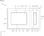
- FIG. 2 is a bottom view showing a semiconductor light emitting device according to the first embodiment of the first group of the present disclosure.
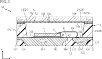
- FIG. 3 is a cross-sectional view taken along the line III-III of FIG.
- FIG. 4 is a cross-sectional view taken along the line IV-IV of FIG.
- FIG. 5 is a cross-sectional view taken along the line VV of FIG.
- FIG. 6 is a partially enlarged view of FIG.
- FIG. 7 is an enlarged cross-sectional perspective view showing a semiconductor light emitting device of the semiconductor light emitting device according to the first embodiment of the first group of the present disclosure.
- FIG. 3 is a cross-sectional view taken along the line III-III of FIG.
- FIG. 4 is a cross-sectional view taken along the line IV-IV of FIG.
- FIG. 5 is a cross-sectional view
- FIG. 8 is an enlarged cross-sectional view of a main part showing a semiconductor light emitting element of the semiconductor light emitting device according to the first embodiment of the first group of the present disclosure.
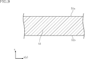
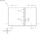
- FIG. 9 is a cross-sectional view showing one step of an example of a method for manufacturing a diffusion cover according to a first embodiment of the first group of the present disclosure.
- FIG. 10 is a cross-sectional view showing the steps following FIG.
- FIG. 11 is a cross-sectional view showing the steps following FIG.
- FIG. 12 is a cross-sectional view showing the steps following FIG.
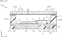
- FIG. 13 is a cross-sectional view similar to FIG. 3 showing a modified example of the semiconductor light emitting device according to the first embodiment of the first group of the present disclosure.
- FIG. 14 is a partially enlarged view of FIG.
- FIG. 15 is a cross-sectional view similar to FIG. 3 showing the semiconductor light emitting device according to the second embodiment of the first group of the present disclosure.
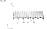
- FIG. 16 is a partially enlarged view of FIG.
- FIG. 17 is a cross-sectional view showing one step of an example of a method for manufacturing a diffusion cover according to a second embodiment of the first group of the present disclosure.
- FIG. 18 is a cross-sectional view showing the steps following FIG.
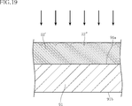
- FIG. 19 is a cross-sectional view showing the steps following FIG.
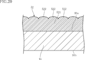
- FIG. 20 is a cross-sectional view showing the steps following FIG.
- FIG. 21 is a perspective view showing a wiring board according to a first embodiment of the second group of the present disclosure.
- FIG. 22 is a plan view showing a wiring board according to a first embodiment of the second group of the present disclosure.
- FIG. 23 is a bottom view showing a wiring board according to the first embodiment of the second group of the present disclosure.
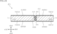
- FIG. 24 is a cross-sectional view taken along the line XXIV-XXIV of FIG.
- FIG. 25 is a partially enlarged cross-sectional view of a part of FIG. 4.
- FIG. 26 is a perspective view showing one step of the method for manufacturing a wiring board according to the first embodiment of the second group of the present disclosure.
- FIG. 27 is a cross-sectional view showing one step of the method for manufacturing a wiring board according to the first embodiment of the second group of the present disclosure.
- FIG. 28 is a cross-sectional view showing one step of the method for manufacturing a wiring board according to the first embodiment of the second group of the present disclosure.
- FIG. 29 is a plan view showing one step of the method for manufacturing a wiring board according to the first embodiment of the second group of the present disclosure.
- FIG. 30 is a cross-sectional view showing one step of the method for manufacturing a wiring board according to the first embodiment of the second group of the present disclosure.
- FIG. 31 is a cross-sectional view showing one step of the method for manufacturing a wiring board according to the first embodiment of the second group of the present disclosure.
- FIG. 32 is a plan view showing one step of the method for manufacturing a wiring board according to the first embodiment of the second group of the present disclosure.
- FIG. 33 is a cross-sectional view showing one step of the method for manufacturing a wiring board according to the first embodiment of the second group of the present disclosure.
- FIG. 34 is a plan view showing one step of the method for manufacturing a wiring board according to the first embodiment of the second group of the present disclosure.
- FIG. 35 is a cross-sectional view showing one step of the method for manufacturing a wiring board according to the first embodiment of the second group of the present disclosure.
- FIG. 36 is a cross-sectional view showing one step of the method for manufacturing a wiring board according to the first embodiment of the second group of the present disclosure.
- FIG. 37 is a plan view showing one step of the method for manufacturing a wiring board according to the first embodiment of the second group of the present disclosure.
- FIG. 38 is a perspective view showing an electronic device including the wiring board according to the first embodiment of the second group of the present disclosure.
- FIG. 39 is a cross-sectional view taken along the line XXXIX-XXXIX of FIG. 38.
- FIG. 40 is a plan view showing a wiring board according to a modified example of the first embodiment of the second group of the present disclosure.
- FIG. 41 is a plan view showing a wiring board according to a modification of the first embodiment of the second group of the present disclosure.
- FIG. 42 is a plan view showing a wiring board according to a modified example of the first embodiment of the second group of the present disclosure.
- FIG. 40 is a plan view showing a wiring board according to a modified example of the first embodiment of the second group of the present disclosure.
- FIG. 43 is a cross-sectional view showing one step of the manufacturing method according to the modified example of the wiring board according to the first embodiment of the second group of the present disclosure.
- FIG. 44 is a cross-sectional view showing one step of the manufacturing method according to the modified example of the wiring board according to the first embodiment of the second group of the present disclosure.
- FIG. 45 is a plan view showing a wiring board according to a second embodiment of the second group of the present disclosure.
- FIG. 46 is a cross-sectional view taken along the line XLVI-XLVI of FIG.
- FIG. 47 is a plan view showing a wiring board according to a modified example of the second embodiment of the second group of the present disclosure.
- FIG. 48 is a plan view showing a wiring board according to a modified example of the second embodiment of the second group of the present disclosure.
- FIG. 49 is a plan view showing a wiring board according to a third embodiment of the second group of the present disclosure.
- FIG. 50 is a plan view showing one step of the method for manufacturing a wiring board according to a third embodiment of the second group of the present disclosure.
- FIG. 51 is a plan view showing a wiring board according to a fourth embodiment of the second group of the present disclosure.
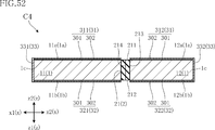
- FIG. 52 is a cross-sectional view taken along the line LII-LII of FIG.
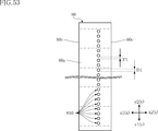
- FIG. 53 is a plan view showing one step of the method for manufacturing a wiring board according to a fourth embodiment of the second group of the present disclosure.
- FIG. 54 is a plan view showing one step of the method for manufacturing a wiring board according to a fourth embodiment of the second group of the present disclosure.
- FIG. 55 is a plan view showing one step of the method for manufacturing a wiring board according to a fourth embodiment of the second group of the present disclosure.
- FIG. 56 is a cross-sectional view taken along the line LVI-LVI of FIG. 35.
- FIG. 57 is a perspective view showing a substrate according to a first embodiment of the third group of the present disclosure.
- FIG. 58 is a plan view showing the substrate according to the first embodiment of the third group of the present disclosure.
- FIG. 59 is a cross-sectional view taken along the line LIX-LIX of FIG. 58.
- FIG. 60 is an enlarged cross-sectional view of a main part showing the substrate according to the first embodiment of the third group of the present disclosure.
- FIG. 61 is a plan view showing a method for manufacturing a substrate according to the first embodiment of the third group of the present disclosure.
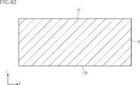
- FIG. 62 is a cross-sectional view taken along the line LXII-LXII of FIG.
- FIG. 63 is a cross-sectional view showing a method of manufacturing a substrate according to the first embodiment of the third group of the present disclosure.
- FIG. 64 is a cross-sectional view showing a method of manufacturing a substrate according to the first embodiment of the third group of the present disclosure.
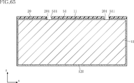
- FIG. 65 is a cross-sectional view showing a method of manufacturing a substrate according to the first embodiment of the third group of the present disclosure.
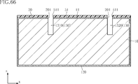
- FIG. 66 is a cross-sectional view showing a method of manufacturing a substrate according to the first embodiment of the third group of the present disclosure.
- FIG. 67 is a plan view showing a method for manufacturing a substrate according to the first embodiment of the third group of the present disclosure.
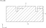
- FIG. 68 is a cross-sectional view taken along the line LXVIII-LXVIII of FIG.
- FIG. 69 is a cross-sectional view showing a method of manufacturing a substrate according to the first embodiment of the third group of the present disclosure.
- FIG. 70 is a cross-sectional view showing a method of manufacturing a substrate according to the first embodiment of the third group of the present disclosure.
- FIG. 71 is an enlarged cross-sectional view of a main part showing a method for manufacturing a substrate according to the first embodiment of the third group of the present disclosure.
- FIG. 72 is a cross-sectional view showing a method of manufacturing a substrate according to the first embodiment of the third group of the present disclosure.
- FIG. 73 is a cross-sectional view showing a method of manufacturing a substrate according to the first embodiment of the third group of the present disclosure.
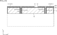
- FIG. 74 is a cross-sectional view showing a method of manufacturing a substrate according to the first embodiment of the third group of the present disclosure.
- FIG. 71 is an enlarged cross-sectional view of a main part showing a method for manufacturing a substrate according to the first embodiment of the third group of the present disclosure.
- FIG. 72 is a cross-sectional view showing a method of manufacturing a substrate according to
- FIG. 75 is a cross-sectional view showing a method of manufacturing a substrate according to the first embodiment of the third group of the present disclosure.
- FIG. 76 is a cross-sectional view showing a method of manufacturing a substrate according to the first embodiment of the third group of the present disclosure.
- FIG. 77 is a cross-sectional view showing a method of manufacturing a substrate according to the first embodiment of the third group of the present disclosure.
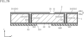
- FIG. 78 is a cross-sectional view showing a method of manufacturing a substrate according to the first embodiment of the third group of the present disclosure.
- FIG. 79 is a cross-sectional view showing a method of manufacturing a substrate according to the first embodiment of the third group of the present disclosure.
- FIG. 80 is a plan view showing a semiconductor device according to the first embodiment of the third group of the present disclosure.
- FIG. 81 is a cross-sectional view taken along the line LXXXI-LXXXI of FIG. 80.
- FIG. 82 is a cross-sectional view showing a first modification of the semiconductor device according to the first embodiment of the third group of the present disclosure.
- FIG. 83 is a plan view showing a substrate according to a second embodiment of the third group of the present disclosure.
- FIG. 84 is a plan view showing a semiconductor device according to a third embodiment of the third group of the present disclosure.
- FIG. 85 is a cross-sectional view taken along the line LXXXV-LXXXV of FIG. 84.
- FIG. 86 is a cross-sectional view showing a method of manufacturing a substrate according to a third embodiment of the third group of the present disclosure.
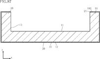
- FIG. 87 is a cross-sectional view showing a method of manufacturing a substrate according to a third embodiment of the third group of the present disclosure.
- FIG. 88 is a cross-sectional view showing a method of manufacturing a substrate according to a third embodiment of the third group of the present disclosure.
- FIG. 89 is a cross-sectional view showing a method of manufacturing a substrate according to a third embodiment of the third group of the present disclosure.
- FIG. 90 is a cross-sectional view showing a method of manufacturing a substrate according to a third embodiment of the third group of the present disclosure.
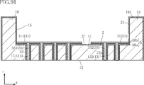
- FIG. 91 is a cross-sectional view showing a method of manufacturing a substrate according to a third embodiment of the third group of the present disclosure.
- something A is formed on a certain thing B
- something A is formed on a certain thing B
- something B means “there is a certain thing A” unless otherwise specified. It includes “being formed directly on the object B” and “being formed on the object B with the object A while interposing another object between the object A and the object B”.
- something A is placed on something B” and “something A is placed on something B” means “something A is placed on something B” unless otherwise specified. It includes "being placed directly on B” and “being placed on a certain thing B while having another thing intervening between a certain thing A and a certain thing B".
- something A is located on something B
- something A is in contact with something B and some thing A is on something B
- something B unless otherwise specified.
- What you are doing and "The thing A is located on the thing B while another thing is intervening between the thing A and the thing B”.
- something A overlaps with some thing B when viewed in a certain direction means “something A overlaps with all of some thing B” and “something A overlaps” unless otherwise specified. "Overlapping a part of a certain object B" is included.
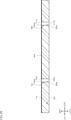
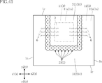
- the semiconductor light emitting device A1 of the present embodiment includes a support 1, a semiconductor light emitting element 4, and a diffusion cover 5.
- FIG. 1 is a plan view of a main part showing the semiconductor light emitting device A1.
- FIG. 2 is a bottom view showing the semiconductor light emitting device A1.
- FIG. 3 is a cross-sectional view taken along the line III-III of FIG.
- FIG. 4 is a cross-sectional view taken along the line IV-IV of FIG.
- FIG. 5 is a cross-sectional view taken along the line VV of FIG.
- FIG. 6 is an enlarged cross-sectional view of a main part showing the semiconductor light emitting device A1, and is a partially enlarged view of FIG.
- FIG. 7 is an enlarged cross-sectional perspective view showing the semiconductor light emitting element 4 of the semiconductor light emitting device A1.
- FIG. 1 is a plan view of a main part showing the semiconductor light emitting device A1.
- FIG. 2 is a bottom view showing the semiconductor light emitting device A1.
- FIG. 3 is a cross-sectional view taken along the line III-III of FIG.
- FIG. 4 is a
- the z direction corresponds to the thickness direction of the first group of the present disclosure.
- the y direction is a direction perpendicular to the z direction
- the x direction is a direction perpendicular to both the y direction and the z direction. Viewing a member along the z direction is called a plan view.
- the support 1 of the present embodiment has a first surface 11, a second surface 12, a third surface 13, a fourth surface 14, a fifth surface 15, a sixth surface 16, a seventh surface 17, and an eighth surface 18. ..
- the first surface 11 is a surface facing one side in the z direction (upper side in FIG. 3).
- the second surface 12 is a surface facing the other side in the z direction (lower side in FIG. 3) opposite to the first surface 11.
- the third surface 13 is a surface facing one side in the z direction (upper side in FIG. 3) like the first surface 11, and is separated from the second surface 12 by the first surface 11.
- the fourth surface 14 is interposed between the first surface 11 and the third surface 13, and is connected to the first surface 11 and the third surface 13 in the present embodiment.
- the fourth surface 14 is an annular shape surrounding the first surface 11 in the z-direction view. Further, the fourth surface 14 is inclined so that the distance between the opposing portions increases from the first surface 11 to the third surface 13 in the z direction.
- the fifth surface 15 is located between the first surface 11 and the third surface 13 in the z direction, and is a surface facing one side in the y direction (right side in FIG. 4). In the illustrated example, the fifth surface 15 is connected to the first surface 11 and the third surface 13.
- the sixth surface 16 is located between the first surface 11 and the third surface 13 in the z direction, and is a surface facing the other side in the y direction (left side in FIG. 4). In the illustrated example, the sixth surface 16 is connected to the first surface 11 and the third surface 13.
- the seventh surface 17 is located between the first surface 11 and the third surface 13 in the z direction, and is a surface facing one side in the x direction (left side in FIG. 3).
- the seventh surface 17 is connected to the first surface 11 and the third surface 13.
- the eighth surface 18 is located between the first surface 11 and the third surface 13 in the z direction, and is a surface facing the other side in the x direction (right side in FIG. 3). In the illustrated example, the eighth surface 18 is connected to the first surface 11 and the third surface 13.
- the configuration of the support 1 is not particularly limited, and in the present embodiment, the support 1 includes the insulating member 2 and the conductive portion 3.
- the insulating member 2 is made of an insulating material, and for example, an epoxy resin, a silicone resin, or the like is appropriately used.
- the insulating member 2 of the present embodiment has a first surface 21, a second surface 22, a third surface 23, a fourth surface 24, a fifth surface 25, a sixth surface 26, a seventh surface 27, and an eighth surface 28. ..
- the first surface 21 faces one side in the z direction and constitutes a part of the first surface 11.
- the second surface 22 faces the other side in the z direction and forms a part of the second surface 12.
- the third surface 23 faces one side in the z direction and constitutes the third surface 13.
- the fourth surface 24 is located between the first surface 21 and the third surface 23 in the z direction, and constitutes the fourth surface 14.
- the fifth surface 25 faces one side in the y direction and constitutes the fifth surface 15.
- the sixth surface 26 faces the other side in the y direction and constitutes the sixth surface 16.
- the seventh surface 27 faces one side in the x direction and constitutes the seventh surface 17.
- the eighth surface 28 faces the other side in the x direction and constitutes the eighth surface 18.
- the conductive portion 3 constitutes a conduction path between the semiconductor light emitting element 4 and the outside of the semiconductor light emitting device A1, and includes the first lead 31 and the second lead 32 in the present embodiment.
- the first lead 31 and the second lead 32 are made of a metal such as Cu, Fe, or Ni.
- the first lead 31 has a first surface 311, a second surface 312, a main portion 315, an edge portion 316, and a plurality of extending portions 317.
- the first surface 311 is a surface facing one side in the z direction and constitutes a part of the first surface 11. In the z-direction view, a part of the first surface 311 is exposed in the region surrounded by the fourth surface 14.
- the second surface 312 is a surface facing the other side in the z direction opposite to the first surface 311 and constitutes a part of the second surface 12. In the illustrated example, the second surface 312 is smaller than the first surface 311 in the z-direction view and is included in the first surface 311.
- the main portion 315 is a portion having the first surface 311 and the second surface 312, and is a portion where both the first surface 311 and the second surface 312 overlap in the z-direction view.
- the edge portion 316 is a portion surrounding the main portion 315 in the z-direction view, and has a part of the first surface 311.
- the other side portion of the edge portion 316 in the z direction is covered with the insulating member 2.
- the plurality of extending portions 317 extend outward from the edge portion 316 in the z-direction view.
- the extending portion 317 has a part of the first surface 311.
- the other side portion of the extending portion 317 in the z direction is covered with the insulating member 2.
- the first lead 31 has three extension 317s.
- One extending portion 317 reaches the fifth surface 25 of the insulating member 2, and the end surface is flush with the fifth surface 25 and is exposed from the fifth surface 25.
- the other one extending portion 317 reaches the sixth surface 26 of the insulating member 2, and the end surface is flush with the sixth surface 26 and is exposed from the sixth surface 26.
- the other one extending portion 317 reaches the seventh surface 27 of the insulating member 2, and the end surface is flush with the seventh surface 27 and is exposed from the seventh surface 27.
- the second lead 32 is arranged so as to be separated from the first lead 31 on the other side in the x direction.
- the second lead 32 has a first surface 321 and a second surface 322, a main portion 325, an edge portion 326, and a plurality of extending portions 327.
- the first surface 321 is a surface facing one side in the z direction and constitutes a part of the first surface 11. In the z-direction view, a part of the first surface 321 is exposed in the region surrounded by the fourth surface 14.
- the second surface 322 is a surface facing the other side in the z direction opposite to the first surface 321 and constitutes a part of the second surface 12. In the illustrated example, the second surface 322 is smaller than the first surface 321 in the z-direction view and is included in the first surface 321.
- the main portion 325 is a portion having the first surface 321 and the second surface 322, and is a portion where both the first surface 321 and the second surface 322 overlap in the z-direction view.
- the edge portion 326 is a portion surrounding the main portion 325 in the z-direction view, and has a part of the first surface 321.
- the other side portion of the edge portion 326 in the z direction is covered with the insulating member 2.
- the plurality of extending portions 327 extend outward from the edge portion 326 in the z-direction view.
- the extending portion 327 has a part of the first surface 321.
- the other side portion of the extending portion 327 in the z direction is covered with the insulating member 2.
- the second lead 32 has three extension 327.
- One extending portion 327 reaches the fifth surface 25 of the insulating member 2, and the end surface is flush with the fifth surface 25 and is exposed from the fifth surface 25.
- the other one extending portion 327 reaches the sixth surface 26 of the insulating member 2, and the end surface is flush with the sixth surface 26 and is exposed from the sixth surface 26.
- the other one extending portion 327 reaches the eighth surface 28 of the insulating member 2, and the end surface is flush with the eighth surface 28 and is exposed from the eighth surface 28.
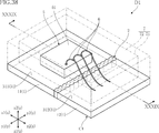
- the semiconductor light emitting element 4 is a light source in the semiconductor light emitting device A1 and emits light in a predetermined wavelength band.
- the specific configuration of the semiconductor light emitting element 4 is not particularly limited, and is a semiconductor laser element, an LED element, or the like.
- the semiconductor light emitting element 4 is a semiconductor laser element, and a VCSEL (Vertical Cavity Surface Emitting Laser) element is adopted.
- the semiconductor light emitting device 4 is die-bonded to the first surface 311 (first surface 11) of the first lead 31 of the conductive portion 3 by the conductive bonding material 48.
- the conductive bonding material 48 is, for example, Ag paste or solder.
- the light from the semiconductor light emitting device 4 is generally emitted to one side in the z direction.
- the semiconductor light emitting device 4 is provided with a first electrode 41 and a plurality of light emitting regions 460 in a plan view.
- the plurality of light emitting regions 460 are discretely arranged in regions other than the first electrode 41 in the plan view of the semiconductor light emitting element 4.
- the semiconductor light emitting device 4 of the present embodiment includes a first electrode 41, a second electrode 42, a substrate 451 and a first semiconductor layer 452, an active layer 453, a second semiconductor layer 454, and a current.
- a constriction layer 455, an insulating layer 456, and a conductive layer 457 are provided, and a plurality of light emitting regions 460 are formed.
- the configuration example shown in the figure is an example of a VCSEL element as the semiconductor light emitting element 4, and is not limited to this configuration.
- FIG. 8 shows an enlarged portion including one light emitting region 460.
- the substrate 451 is made of a semiconductor.
- the semiconductor constituting the substrate 451 is, for example, an n-type GaAs.
- the semiconductor constituting the substrate 451 may be other than GaAs.
- the active layer 453 is composed of a compound semiconductor that emits light having a wavelength in the 980 nm band (hereinafter referred to as “ ⁇ a”) by spontaneous emission and stimulated emission, for example.
- the active layer 453 is located between the first semiconductor layer 452 and the second semiconductor layer 454.
- the structure is composed of a multiple quantum well structure in which an undoped GaAs well layer and an undoped AlGaAs barrier layer (barrier layer) are alternately laminated.
- the undoped Al 0.35 Ga 0.65 As barrier layer and the undoped GaAs well layer are alternately and repeatedly formed for 2 to 6 cycles.
- the first semiconductor layer 452 is typically a DBR (Distributed Bragg Reflector) layer, and is formed on the substrate 451.
- the first semiconductor layer 452 is made of a semiconductor having a first conductive type. In this example, the first conductive type is n type.
- the first semiconductor layer 452 is configured as a DBR for efficiently reflecting the light emitted from the active layer 453.
- the first semiconductor layer 452 is formed by stacking a plurality of pairs of AlGaAs layers having a thickness of ⁇ a / 4 and having different reflectances in a plurality of stages.
- the first semiconductor layer 452 has, for example, an n-type Al 0.16 Ga 0.84 As layer (low Al composition layer) having a thickness of 600 ⁇ and a relatively low Al composition, and a thickness of, for example, 700 ⁇ .
- the n-type Al 0.92 Ga 0.16 As layer (high Al composition layer) having a relatively high Al composition is alternately and repeatedly laminated for a plurality of cycles (for example, 20 cycles).
- the n-type Al 0.16 Ga 0.84 As layer and the n-type Al 0.92 Ga 0.16 As layer are, for example, 2 ⁇ 10 17 cm -3 to 3 ⁇ 10 18 cm -3 and 2 ⁇ 10 17 cm -3 to 3 ⁇ 10, respectively. It is doped with n-type impurities (eg Si) at a concentration of 18 cm -3.
- the current constriction layer 455 is located in the second semiconductor layer 454.
- the current constriction layer 455 is composed of, for example, a layer containing a large amount of Al and easily oxidized.
- the current constriction layer 455 is formed by oxidizing this easily oxidizable layer.
- the current constriction layer 455 does not necessarily have to be formed by oxidation, but may be formed by other methods (eg, ion implantation).
- An opening 4551 is formed in the current constriction layer 455. Current flows through the opening 4551.
- the insulating layer 456 is formed on the second semiconductor layer 454.
- the insulating layer 456 is made of, for example, SiO 2 .
- An opening 4651 is formed in the insulating layer 456.
- the conductive layer 457 is formed on the insulating layer 456.
- the conductive layer 457 is made of a conductive material (for example, metal).
- the conductive layer 457 is conductive to the second semiconductor layer 454 through the opening 4651 of the insulating layer 456.
- the conductive layer 457 has an opening 4571.
- the light emitting region 460 is a region where the light from the active layer 453 is emitted directly or after reflection.
- the light emitting region 460 has a circular ring shape in a plan view, but the shape is not particularly limited.
- the second semiconductor layer 454, the current constriction layer 455, the insulating layer 456 and the conductive layer 457 are laminated, and the opening 4551 of the current constriction layer 455, the opening 4651 of the insulating layer 456 and the opening 4571 of the conductive layer 457 are laminated. Etc. are provided by forming.
- the light from the active layer 453 is emitted through the opening 4571 of the conductive layer 457.
- the first electrode 41 is made of metal, for example, and conducts to the second semiconductor layer 454.
- the second electrode 42 is formed on the back surface of the substrate 451 and is made of, for example, metal.
- the second electrode 42 is die-bonded to the first surface 311 by, for example, a paste containing a metal such as Ag or a conductive bonding material 48 such as solder (see FIG. 3). As a result, the second electrode 42 is electrically connected to the first lead 31 of the conductive portion 3.
- the wire 49 is connected to the first electrode 41 of the semiconductor light emitting element 4 and the first surface 321 of the second lead 32.
- the material of the wire 49 is not particularly limited, and is made of, for example, Au.
- four wires 49 are provided in parallel with each other.
- the number and arrangement of the wires 49 are not particularly limited.
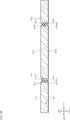
- the diffusion cover 5 closes the semiconductor light emitting element 4 in the z-direction, and diffuses and transmits the light from the semiconductor light emitting element 4.
- the diffusion cover 5 includes a base material 51 and a lens body 52.
- the diffusion cover 5 is joined to the third surface 13 (third surface 23) of the support 1 by, for example, a joining member 57.
- the joining material 57 is an insulating adhesive made of, for example, a resin material.
- the base material 51 is made of a material that transmits light from the semiconductor light emitting element 4 such as glass.
- the base material 51 is made of a transparent glass substrate.
- the shape of the base material 51 and the like are not particularly limited, and in the present embodiment, the base material 51 has a rectangular shape.
- the base material 51 has a front surface 51a and a back surface 51b.
- the front surface 51a and the back surface 51b face each other in the z direction.
- the back surface 51b faces one side in the z direction (upper side in FIG. 3).
- the surface 51a faces the other side in the z direction (lower side in FIG. 3) and faces the semiconductor light emitting device 4.
- the front surface 51a and the back surface 51b are flat surfaces.
- the front surface 51a and the back surface 51b have sizes that correspond to the entire base material 51 in the z-direction view.
- the thickness (dimension in the z direction) of the base material 51 is not particularly limited, and is, for example, about 300 ⁇ m to 725 ⁇ m.
- the lens body 52 is arranged on the surface 51a of the base material 51, and transmits the light from the semiconductor light emitting element 4 while diffusing it.
- the lens body 52 is made of a transparent resin such as an acrylic resin.
- the lens body 52 has a base layer 521 and a plurality of lens portions 522.
- the base layer 521 is a portion that is in close contact with the surface 51a of the base material 51 and is laminated on the surface 51a. In the present embodiment, the base layer 521 covers the entire surface 51a.
- the plurality of lens units 522 have a function of diffusing the light from the semiconductor light emitting element 4.
- the plurality of lens portions 522 are integrally connected on the base layer 521, and each is composed of a curved lens having a convex shape on the other side in the z direction (the same side as the surface 51a).
- the plurality of lens units 522 are arranged in both the x-direction and the y-direction in the z-direction view, and form a microlens array.
- the plurality of lens units 522 are formed by performing grayscale exposure and development, which will be described later.
- the dimensions of each part of the lens body 52 shown in FIG. 6 are not particularly limited.
- the first dimension L1 and the second dimension L2 will be described.
- the first dimension L1 is the length of the lens body 52 in the z direction.
- the first dimension L1 includes the apex of the lens body 52 in the z direction (the point that protrudes most toward the lower side in FIG. 6) and the bottom surface (the surface located on the opposite side of the apex in the z direction).
- the second dimension L2 is the length of the lens portion 522 in the z direction.
- the second dimension L2 is the distance between the apex of the lens body 52 in the z direction and the boundary surface (represented by a broken line in FIG.
- the first dimension L1 is, for example, 1 ⁇ m to 10 ⁇ m, preferably 2 ⁇ m to 7 ⁇ m.
- the second dimension L2 is, for example, 1 ⁇ m to 10 ⁇ m, preferably 2 ⁇ m to 6 ⁇ m. Further, the ratio of the first dimension L1 to the second dimension L2 is, for example, 1 to 3 times.
- the lens body 52 shown in FIGS. 3 to 5 has a lens region 52A and a non-lens region 52B.
- the lens region 52A is a region in which a plurality of lens portions 522 are formed in the lens body 52.
- the lens region 52A is surrounded by the third surface 13 (third surface 23) of the support 1 in the z-direction view.
- the non-lens region 52B is a region in which a plurality of lens portions 522 are not formed in the lens body 52.
- the non-lens region 52B surrounds the lens region 52A in the z-direction view.
- the non-lens region 52B is formed in a region corresponding to the third surface 13 (third surface 23) of the support 1.
- the non-lens region 52B is arranged so as to face the third surface 13 (third surface 23).
- the bonding material 57 is interposed between the third surface 13 (third surface 23) and the non-lens region 52B.
- the bonding material 57 is formed in a region that overlaps the third surface 13 (third surface 23) and the non-lens region 52B in the z-direction view.
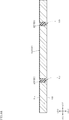
- FIGS. 9 to 12 An example of a method for manufacturing the diffusion cover 5 will be described below with reference to FIGS. 9 to 12.
- a method of forming one diffusion cover 5 is described for convenience of understanding, but the present disclosure is not limited to this, and a material capable of collectively manufacturing a plurality of diffusion covers 5 is described.
- a plurality of diffusion covers 5 may be manufactured by appropriately performing a division step or the like using the above.
- the base material 51 is prepared.
- the base material 51 is made of, for example, a transparent glass substrate.
- the base material 51 has a front surface 51a and a back surface 51b.
- the front surface 51a and the back surface 51b are planes facing opposite to each other in the thickness direction of the base material 51.
- the lens material 52' is formed on the surface 51a of the base material 51.
- the lens material 52' is a material member to be a lens body 52, and is made of a photosensitive transparent resin obtained by imparting positive photosensitivity to a transparent resin such as an acrylic resin.
- the method for forming the lens material 52' is not particularly limited, but the lens material 52'is formed by, for example, applying a photosensitive transparent resin on the surface 51a of the base material 51 to a predetermined film thickness by a spin coating method and drying the lens material 52'.
- the thickness of the lens material 52' is about the same as the first dimension L1 in the z direction (thickness direction) of the lens body 52 described above.
- the lens material 52' is exposed.
- the photosensitive transparent resin constituting the lens material 52' has positive photosensitivity, and the exposure process is performed by irradiating light having a predetermined wavelength from the lens material 52'side.
- a grayscale exposure method is adopted.
- the specific method of grayscale exposure is not limited, and examples thereof include a method of changing the intensity of light applied to the lens material 52'and a method of using a multi-gradation mask such as a gray tone mask.
- the exposure process is performed on the formation region (lens region 52A) of the plurality of lens portions 522. Further, the exposed portion of the lens material 52'by the exposure process (grayscale exposure) (represented by reference numeral 52 "in FIG. 11) corresponds to the shape of each lens portion 522.
- the development process is performed.
- a part of the lens material 52'(exposed portion 52') is removed to form a plurality of lens portions 522.
- a heat treatment is performed.
- a diffusion cover 5 in which the lens body 52 is arranged is formed on the surface 51a of the material 51.
- the lens body 52 made of transparent resin has a plurality of lens portions 522.
- the formation of the plurality of lens portions 522 is performed by performing grayscale exposure and development on the lens material 52'made of a photosensitive resin material and removing a part of the lens material 52'. According to such a configuration of the diffusion cover 5, the manufacturing cost of the diffusion cover 5 can be reduced as compared with the case where a plurality of lens portions are formed by using, for example, an imprint device.
- the photosensitive transparent resin constituting the lens material 52' has positive photosensitivity.
- the grayscale exposure to the lens material 52'formed on the base material 51 is performed by irradiating light from the lens material 52'side. According to such a configuration, it is possible to appropriately form a plurality of lens portions 522 from the lens material 52'formed on the base material 51.
- the embossing required in the case of the imprint method, for example, is unnecessary.
- the first dimension L1 of the lens body 52 in the z direction (thickness direction) can be as small as about 1 ⁇ m to 10 ⁇ m. Therefore, the amount of the lens material 52'used can be reduced, which is suitable for reducing the manufacturing cost of the diffusion cover 5.
- the lens body 52 has a lens region 52A in which a plurality of lens portions 522 are formed, and a non-lens region 52B in which the lens portion 522 is not formed.
- the non-lens region 52B surrounds the lens region 52A in the z-direction view and faces the third surface 13 (third surface 23) of the support 1. According to the configuration in which the non-lens region 52B is provided, the light from the semiconductor light emitting element 4 can be directed to the lens region 52A, and the diffusion cover 5 can be appropriately supported by the support 1.
- ⁇ Modified example of the first embodiment> 13 and 14 show a modification of the semiconductor light emitting device A1 according to the first embodiment described above.
- the same or similar elements as the semiconductor light emitting device A1 of the above embodiment are designated by the same reference numerals as those of the above embodiment, and the description thereof will be omitted as appropriate.
- the configuration of the lens body 52 of the diffusion cover 5 is different from that of the semiconductor light emitting device A1 of the above embodiment.
- the plurality of lens portions 522 of the lens body 52 are directly formed on the surface 51a of the base material 51.
- the base layer 521 is not interposed between the plurality of lens portions 522 and the base material 51.
- a portion of the surface 51a corresponding to the lens region 52A where the lens portion 522 is not formed is not covered by the lens body 52 and is exposed.
- the lens body 52 having such a configuration can be obtained by making the thickness of the lens material 52'smaller than that of the above embodiment, for example, when the lens body 52 is formed (see FIGS. 11 and 12). Further, the exposed portion 52 "of the lens material 52'by grayscale exposure is centered on the deepest portion along the z direction without changing the position in the x direction shown in FIG.
- the lens body 52 of this modification can also be obtained by expanding the lens in the x-direction and the y-direction.
- the semiconductor light emitting device A11 of this modification can also reduce the manufacturing cost of the diffusion cover 5 as compared with the case where a plurality of lens portions are formed by using, for example, an imprint device.
- the semiconductor light emitting device A11 also has the same effect as described above with respect to the semiconductor light emitting device A1.
- ⁇ Second Embodiment> 15 and 16 show the semiconductor light emitting device according to the second embodiment of the first group of the present disclosure.
- the semiconductor light emitting device A2 of the present embodiment is different from the semiconductor light emitting device A1 of the above embodiment in the configuration of the diffusion cover 5.
- the diffusion cover 5 does not include the base material 51 and is composed of only the lens body 52.
- the lens body 52 has a base layer 521 and a plurality of lens portions 522.
- the dimension of the base layer 521 in the z direction is larger than that of the above embodiment.
- FIGS. 17 to 20 An example of the manufacturing method of the diffusion cover 5 of the present embodiment will be described below with reference to FIGS. 17 to 20.
- a method of forming one diffusion cover 5 is described for convenience of understanding, but the present disclosure is not limited to this, and a material capable of collectively manufacturing a plurality of diffusion covers 5 is described.
- a plurality of diffusion covers 5 may be manufactured by appropriately performing a division step or the like using the above.
- the base material 91 is prepared.
- the base material 91 is made of, for example, a silicon substrate.
- the base material 91 has a front surface 91a and a back surface 91b.
- the front surface 91a and the back surface 91b are planes facing opposite to each other in the thickness direction of the base material 91.
- the lens material 52' is formed on the surface 91a of the base material 91.
- the lens material 52' is a material member to be a lens body 52, and is made of a photosensitive transparent resin obtained by imparting positive photosensitivity to a transparent resin such as an acrylic resin.
- the method for forming the lens material 52' is not particularly limited, but for example, it is performed by printing a thick film of a photosensitive transparent resin on the surface 91a of the base material 91 and then firing the film.
- the lens material 52' is exposed.
- the photosensitive transparent resin constituting the lens material 52' has positive photosensitivity, and the exposure process is performed by irradiating light having a predetermined wavelength from the lens material 52'side.
- a grayscale exposure method is adopted.
- the specific method of grayscale exposure is not limited, and examples thereof include a method of changing the intensity of light applied to the lens material 52'and a method of using a multi-gradation mask such as a gray tone mask.
- the exposure process is performed on the formation region (lens region 52A) of the plurality of lens portions 522. Further, the exposed portion 52 "of the lens material 52'by the exposure process (grayscale exposure) corresponds to the shape of each lens portion 522.
- the development process is performed.
- a part of the lens material 52'(exposed portion 52') is removed to form a plurality of lens portions 522.
- a heat treatment is performed.
- the lens body 52 is formed on the surface 91a of the material 91.
- the lens body 52 is peeled off from the base material 91.
- the lens body 52 thus peeled off from the base material 91 constitutes the diffusion cover 5.
- the semiconductor light emitting device A2 of the present embodiment can also reduce the manufacturing cost of the diffusion cover 5 as compared with the case where a plurality of lens portions are formed by using, for example, an imprint device.
- the semiconductor light emitting device A2 also exhibits the same effects as the semiconductor light emitting device A1 within the range of the same configuration as the semiconductor light emitting device A1.
- the semiconductor light emitting device according to the first group of the present disclosure is not limited to the above-described embodiment.
- the specific configuration of each part of the semiconductor light emitting device according to the first group of the present disclosure can be freely redesigned.
- the first group of the present disclosure includes the configurations relating to the following appendices A1 to A16.
- Appendix A1 A method for manufacturing a diffusion cover that diffuses and transmits light from a semiconductor light emitting device. A step of preparing a base material having a front surface and a back surface facing opposite to each other in the thickness direction, and A step of forming a lens material containing a photosensitive transparent resin on the surface, and A method for manufacturing a diffusion cover, comprising a step of removing a part of the lens material by performing grayscale exposure and development to form a lens body having a plurality of lens portions.
- the photosensitive transparent resin has positive photosensitivity and has positive photosensitivity. The method for manufacturing a diffusion cover according to Appendix A1, wherein the grayscale exposure is performed by irradiating light from the lens material side.
- the base material includes a silicon substrate and contains a silicon substrate. A step of peeling the lens body from the base material, which is performed after the step of forming the lens body, is further provided.
- a diffusion cover that diffuses and transmits light from semiconductor light emitting elements.
- a substrate having a front surface and a back surface facing each other in the thickness direction, A diffusion cover which is arranged on the surface, has a plurality of convex lens portions on the same side as the surface in the thickness direction, and includes a lens body containing a transparent resin.
- the lens body has a base layer that is in close contact with the surface.
- the diffusion cover according to Appendix A7, wherein the plurality of lens portions are integrally connected on the base layer.
- the support has a first surface on which the semiconductor light emitting element is arranged and facing the thickness direction, a second surface facing the side opposite to the first surface, facing the same side as the first surface, and the first surface. It has a third surface that is separated from the second surface by a surface and surrounds the first surface in the thickness direction view, and a fourth surface that is interposed between the first surface and the third surface.
- the semiconductor light emitting device according to Appendix A13, wherein the diffusion cover is supported on the third surface.
- the lens body has a lens region in which the plurality of lens portions are formed, and a non-lens region that surrounds the lens region in the thickness direction view and in which the plurality of lens portions are not formed.
- the semiconductor light emitting device according to Appendix A14, wherein the diffusion cover is arranged such that the non-lens region faces the third surface.
- the semiconductor light emitting device according to any one of Appendix A13 to 15, wherein the semiconductor light emitting element is a VCSEL element.
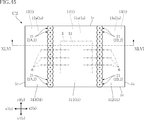
- the wiring board C1 includes a base material 1, an insulating portion 2, a main surface electrode 31, and a back surface electrode 32.
- FIG. 21 is a perspective view showing the wiring board C1.
- FIG. 22 is a plan view showing the wiring board C1.
- FIG. 23 is a bottom view showing the wiring board C1.
- FIG. 24 is a cross-sectional view taken along the line XXIV-XXIV of FIG.
- FIG. 25 is a partially enlarged cross-sectional view of a part of FIG. 24.
- the three directions orthogonal to each other are defined as the x direction, the y direction, and the z direction.
- the z direction is the thickness direction of the wiring board C1.
- the x direction is the left-right direction in the plan view (see FIG. 22) of the wiring board C1.
- the y direction is the vertical direction in the plan view (see FIG. 22) of the wiring board C1.
- One in the x direction is the x1 direction
- the other in the x direction is the x2 direction.
- one in the y direction is the y1 direction
- the other in the y direction is the y2 direction
- one in the z direction is the z1 direction
- the other in the z direction is the z2 direction.
- plane view means when viewed in the z direction.
- the wiring board C1 is a member for forming an electronic device together with electronic components and mounting the electronic device on a circuit board.
- the wiring board C1 has a plate shape, and the shape in a plan view is, for example, a rectangular shape.
- the base material 1 contains a semiconductor material.
- the base material 1 contains, for example, single crystal Si (silicon) as a main component and is doped with impurities for increasing conductivity.
- This impurity is a p-type impurity such as B (boron), Al (aluminum), and Ga (gallium).
- the constituent material of the base material 1 is not particularly limited, but it is desirable that the joining technique is established and the relatively inexpensive Si is the main component.
- a semiconductor material doped with n-type impurities may be used as the base material 1, a semiconductor material doped with n-type impurities may be used. In the example shown in FIGS. 22 and 23, the base material 1 has, for example, a rectangular shape in a plan view.
- the base material 1 has a main surface 1a, a back surface 1b, and a plurality of side surfaces 1c.
- the main surface 1a and the back surface 1b are separated from each other in the z direction.
- the main surface 1a and the back surface 1b are, for example, flat and substantially orthogonal to the z direction.
- the main surface 1a faces the z2 direction, and the back surface 1b faces the z1 direction.
- the lattice plane of the main plane 1a is, for example, a (100) plane.
- the plurality of side surfaces 1c are connected to the main surface 1a and the back surface 1b, respectively, and are sandwiched between the main surface 1a and the back surface 1b in the z direction.
- the base material 1 Since the base material 1 has a rectangular shape in a plan view, the base material 1 has four side surfaces 1c as shown in FIGS. 22 and 23. Of the four side surfaces 1c, two side surfaces 1c are separated in the x direction and face each other, and the other two side surfaces 1c are separated in the y direction and face each other.
- the base material 1 includes the first part 11 and the second part 12.
- the first part 11 and the second part 12 are separated by sandwiching the insulating part 2 and insulate each other.
- the first part 11 is located on the x1 direction side of the insulating part 2
- the second part 12 is located on the x2 direction side of the insulating part 2.
- the first part 11 and the second part 12 have, for example, a rectangular shape in a plan view, respectively.
- Part 1 11 has a first main surface 11a and a first back surface 11b.
- the first main surface 11a and the first back surface 11b are separated from each other in the z direction.
- the first main surface 11a faces the z2 direction, and the first back surface 11b faces the z1 direction.
- the second part 12 has a second main surface 12a and a second back surface 12b.
- the second main surface 12a and the second back surface 12b are separated from each other in the z direction.
- the second main surface 12a faces the z2 direction, and the second back surface 12b faces the z1 direction.
- the main surface 1a is formed by the first main surface 11a and the second main surface 12a.
- the back surface 1b is formed by the first back surface 11b and the second back surface 12b.
- the insulating portion 2 separates the first portion 11 and the second portion 12.
- the insulating portion 2 is made of an insulating material, and is, for example, an oxide of a constituent material of the base material 1.
- the insulating portion 2 is, for example, SiO 2 (silicon oxide).
- the insulating portion 2 is linear in a plan view.
- the insulating portion 2 is connected in the y direction from the side surface 1c in the y1 direction to the side surface 1c in the y2 direction in a plan view.
- the insulating portion 2 includes a plurality of penetrating portions 21.
- Each of the plurality of penetrating portions 21 penetrates the base material 1 from the main surface 1a to the back surface 1b in the z direction.
- Each penetrating portion 21 has a substantially circular cross section orthogonal to the z direction.
- the plurality of penetrating portions 21 are arranged in the y direction in the plan view, and the two adjacent penetrating portions 21 are connected to each other in the plan view. As a result, the plurality of penetrating portions 21 are connected to each other to form the insulating portion 2.
- Each penetrating portion 21 has a main surface 211, a back surface 212, a side surface 213, and a boundary portion 214, respectively.
- the main surface 211 and the back surface 212 are separated from each other in the z direction.
- the main surface 211 faces the z2 direction, and the back surface 212 faces the z1 direction.
- the main surface 211 is substantially flush with the main surface 1a (first main surface 11a and second main surface 12a).
- the back surface 212 is substantially flush with the back surface 1b (first back surface 11b and second back surface 12b).
- the side surface 213 is connected to the main surface 211 and the back surface 212, and is sandwiched between the main surface 211 and the back surface 212 in the z direction.
- the side surface 213 has a stepped structure that is wavy when viewed from a direction orthogonal to the z direction.
- the boundary portion 214 is located substantially at the center of each penetration portion 21 in a plan view.
- the boundary portion 214 extends in the z direction, for example, and is connected from the main surface 211 to the back surface 212.
- the boundary portion 214 is a trace formed in the manufacturing method described later.
- the main surface electrode 31 covers the main surface 1a of the base material 1.
- the main surface electrode 31 includes a first main surface covering portion 311 and a second main surface covering portion 312.
- the first main surface covering portion 311 covers the first main surface 11a (first portion 11).
- the second main surface covering portion 312 covers the second main surface 12a (second main surface 12).
- the back surface electrode 32 covers the back surface 1b of the base material 1.
- the back surface electrode 32 includes a first back surface covering portion 321 and a second back surface covering portion 322.
- the first back surface covering portion 321 covers the first back surface 11b (first portion 11).
- the second back surface covering portion 322 covers the second back surface 12b (second portion 12).
- the back surface electrode 32 is used as an external electrode when the wiring board C1 is mounted on a circuit board such as an electronic device.
- the base material 1 (first part 11 and second part 12) is made of a semiconductor material
- the first main surface covering part 311 and the first back surface covering part 321 are conductive via the first part 11.
- the second main surface covering portion 312 and the second back surface covering portion 322 are electrically connected to each other via the second portion 12.
- the base material 1 is subjected to a treatment for increasing the conductivity (impurity doping)
- the first main surface coating portion 311 and the first back surface coating portion 321 are electrically connected to each other and the first back surface coating portion 321 is connected. 2
- the continuity between the main surface covering portion 312 and the second back surface covering portion 322 becomes better.
- the main surface electrode 31 and the back surface electrode 32 include, for example, a first metal layer 301 and a second metal layer 302 laminated in the z direction, respectively.
- the main surface electrode 31 and the back surface electrode 32 may have different configurations.
- the first metal layer 301 is in contact with the base material 1. That is, the first metal layer 301 is laminated on each of the main surface 1a (first main surface 11a and second main surface 12a) and the back surface 1b (first back surface 11b and second back surface 12b).
- the constituent material of the first metal layer 301 contains, for example, Al.
- the constituent material of the first metal layer 301 is not limited to Al, and the first metal layer 301 may have a structure in which a plurality of metal layers are laminated.
- the second metal layer 302 is laminated on the first metal layer 301 and is in contact with the first metal layer 301.
- the second metal layer 302 is each surface layer of the main surface electrode 31 and the back surface electrode 32.
- the second metal layer 302 is laminated in the order of, for example, the Au (gold) layer, the Ni (nickel) layer, the Ag (silver) layer, and the Au layer from the side in contact with the first metal layer 301.
- the configuration of the second metal layer 302 is not limited to the above example.
- the second metal layer 302 may be laminated in the order of the Ni layer and the Au layer from the side in contact with the first metal layer 301, or the Ni layer, the Pd (palladium) layer, and the Au layer in this order. It may be a laminated structure.
- the main surface electrode 31 and the back surface electrode 32 are not each composed of two metal layers (first metal layer 301 and second metal layer 302) laminated, but are composed of one metal layer (for example, Au layer). You may be.
- FIGS. 26 to 37 are diagrams showing one step of the manufacturing method of the wiring board C1, respectively.
- FIG. 26 is a perspective view showing one step of the manufacturing method.
- 27, 28, 30, 31, 31, 33, 35 and 36 are cross-sectional views showing one step of the manufacturing method. These cross-sectional views correspond to the cross-sectional views of FIG. 24 of the wiring board C1.
- 29, 32, 34 and 37 are plan views showing one step of the manufacturing method.
- the size of each component shown in FIGS. 26 to 37 is appropriately made larger than the size of each component shown in FIGS. 21 to 25.
- a semiconductor wafer 81 is prepared.
- wafer preparation step for example, when a single crystal Si ingot is prepared, a p-type impurity is added and the ingot is sliced thinly to form the semiconductor wafer 81.
- the semiconductor wafer 81 has a wafer main surface 81a and a wafer back surface 81b.
- the wafer main surface 81a and the wafer back surface 81b are separated from each other in the z direction.
- the wafer main surface 81a and the wafer back surface 81b are substantially flat and are substantially orthogonal to each other in the z direction.
- the wafer main surface 81a faces the z2 direction, and the wafer back surface 81b faces the z1 direction.
- the semiconductor wafer 81 shown in FIG. 26 is circular in a plan view, but may have a notch, an orientation flat, or the like. In the drawings after FIG. 27, regions corresponding to the four wiring boards C1 are extracted and described.
- the step of forming the insulating portion 82 includes the following three steps. These three steps are a through hole forming step, a thermal oxidation step, and a grinding step.
- the through hole forming step includes, for example, the following three steps.
- the resist film 819 is patterned by, for example, photolithography. Specifically, a resist film 819 is formed on substantially the entire surface of the wafer main surface 81a of the semiconductor wafer 81, and the resist film 819 is appropriately exposed and etched to pattern the resist film 819. As shown in FIG. 27, the patterned resist film 819 has an opening 819a, and a portion of the semiconductor wafer 81 (wafer main surface 81a) forming a plurality of through holes 810 is formed from the opening 819a. Be exposed.
- a plurality of through holes 810 are formed by etching the semiconductor wafer 81 exposed from the resist film 819.
- etching for example, deep RIE (Reactive Ion Etching), which is one of the reactive etchings, is adopted.
- the etching method is not limited to deep RIE.
- the third step of the through hole forming step removes the resist film 819 as shown in FIGS. 29 and 30.
- the method for removing the resist film 819 is not particularly limited.
- each through hole 810 formed has a pair of openings 810a, 810b and a side wall 810c, as shown in FIG.
- the opening 810a opens at the wafer main surface 81a, and the opening 810b opens from the wafer back surface 81b.
- the pair of openings 810a and 810b are circular in a plan view, respectively.
- the side wall 810c is connected to each of the pair of openings 810a and 810b. Since each through hole 810 is formed by deep RIE, the side wall 810c has a stepped structure called a scallop. Further, as shown in FIG.
- the plurality of through holes 810 are arranged in the y direction.
- the two through holes 810 adjacent to each other in the y direction are arranged with a predetermined interval P1.
- the interval P1 is not particularly limited, but in one example, it is about 0.5 ⁇ m to 4.0 ⁇ m (preferably about 0.9 ⁇ m). Therefore, the plurality of through holes 810 are separated from each other. Further, each through hole 810 has a diameter D1 of about 1 ⁇ m to 3 ⁇ m in a plan view.
- the semiconductor wafer 81 is thermally oxidized to form an oxide film 820.
- the oxide film 820 is an oxide of a constituent material of the semiconductor wafer 81.
- the formed oxide film 820 includes a plurality of penetration portions 821 and a surface portion 822. At this point, the plurality of penetrating portions 821 and the surface portion 822 are connected to each other.
- Each penetration 821 has a side surface 821c and a boundary 821d, as shown in FIGS. 31 and 32.
- the side surface 821c corresponds to the side surface 213 of the wiring board C1
- the boundary portion 821d corresponds to the boundary portion 214 of the wiring board C1.
- an oxide film 820 is formed on the surface of the semiconductor wafer 81 that comes into contact with the outside air.
- the oxide film 820 is formed from the side wall 810c of each through hole 810 toward both the radial inner side and the radial outer side of each through hole 810 in a plan view.
- the oxide film 820 growing in the x2 direction from the side wall 810c and the oxide film 820 growing in the x1 direction come into contact with each other near the center of the through hole 810 in a plan view. Although they interact with each other, they do not integrate even if the oxide films 820 come into contact with each other. Therefore, the boundary portion 821d is formed in the penetrating portion 821. Further, by forming the oxide film 820 outward in the radial direction of each through hole 810, the two adjacent through portions 821 are connected to each other. The larger the interval P1, the longer it takes to form the oxide film 820 by thermal oxidation until the two adjacent penetrating portions 821 are connected to each other. Therefore, as described above, the interval P1 is preferably about 0.9 ⁇ m.
- the surface portions 822 formed on the wafer main surface 81a and the wafer back surface 81b of the semiconductor wafer 81 are ground.
- the wafer main surface 81a and the wafer back surface 81b are exposed by the grinding process.
- the semiconductor wafer 81 may be ground together with the grinding of the surface portion 822.
- a main surface 821a that is substantially flush with the wafer main surface 81a and a back surface 821b that is substantially flush with the wafer back surface 81b are formed on each through portion 821.
- the insulating portion 82 is formed on the semiconductor wafer 81 as shown in FIGS. 33 and 34.
- the insulating portion 82 penetrates the semiconductor wafer 81 from the wafer main surface 81a to the wafer back surface 81b in the z direction.
- the insulating portion 82 is configured by connecting a plurality of penetrating portions 821 to each other.
- the step of forming the main surface electrode 831 (main surface electrode forming step) and the step of forming the back surface electrode 832 (back surface electrode forming step) include a first metal layer forming step and a second metal layer forming step, respectively.
- the first metal layer 830a covering the wafer main surface 81a and the wafer back surface 81b is formed.
- a metal film is formed on the entire surface of the wafer main surface 81a and the wafer back surface 81b by, for example, a sputtering method or a vapor deposition method.
- the constituent material of this metal film is, for example, Al.
- the metal film is patterned by photolithography. As a result, the first metal layer 830a is formed.
- the formed first metal layer 830a is not formed on the front surface of the insulating portion 82 (the main surface 821a and the back surface 821b of each penetrating portion 821).
- the second metal layer forming step forms a second metal layer 830b that covers the first metal layer 830a, as shown in FIGS. 36 and 37.
- the second metal layer forming step is performed by, for example, electroless plating.
- the Au layer in contact with the first metal layer 830a is precipitated by electroless plating, and then the Ni layer, the Ag layer, and the Au layer are precipitated in this order. Therefore, in the present embodiment, the constituent material of the second metal layer 830b is composed of a plurality of laminated metal layers, for example, from the side in contact with the first metal layer 830a, the Au layer, the Ni layer, the Ag layer, and the Au layer. They are stacked in order.
- the second metal layer forming step is appropriately changed according to the configuration of the second metal layer 302 on the wiring board C1.
- the main surface electrode 831 including the first metal layer 301 and the second metal layer 302, and the first metal layer 301 and the second metal layer 302 The back surface electrode 832 including the above is formed. That is, by performing the first metal layer forming step and the second metal layer forming step, the main surface electrode forming step and the back surface electrode forming step are collectively performed. Either one of the main surface electrode forming step and the back surface electrode forming step may be performed first, and the other may be performed after that.
- the semiconductor wafer 81 is cut along the cutting line CL shown in FIGS. 36 and 37, and the semiconductor wafer 81 is fragmented into the final product shape.
- a dicing blade is used for cutting the semiconductor wafer 81, for example.
- the cutting line CL is shown in a strip shape in consideration of the thickness of the dicing blade.
- the wiring board C1 shown in FIGS. 21 to 25 is manufactured. That is, a wiring board C1 including a base material 1 (first part 11 and second part 12), an insulating part 2 (a plurality of penetrating parts 21), a main surface electrode 31 and a back surface electrode 32 is manufactured.
- FIG. 38 is a perspective view showing an electronic device D1 including a wiring board C1.
- FIG. 39 is a cross-sectional view taken along the line XXXIX-XXXIX of FIG. 38.
- the electronic device D1 includes a wiring board C1, an electronic component 5, a plurality of bonding wires 6, and a resin member 7.
- the resin member 7 is shown by an imaginary line (dashed-dotted line) in FIG. 38.
- the electronic component 5 is an element that exerts an electrical function of the electronic device D1.
- the electronic component 5 is, for example, a VCSEL element.
- the electronic component 5 (VCSEL element) emits light in a predetermined wavelength band and serves as a light source for the electronic device D1.
- the electronic component 5 is not limited to the VCSEL element, and may be another light emitting element such as an LED element, a semiconductor element (active element) such as a transistor, a diode, or an IC, or a passive element such as a resistor, a capacitor, or an inductor. .. It is preferable that the electronic component 5 has a large heat generating property among the light emitting element and the active element of the power system.
- the electronic component 5 has a main surface 51 and a back surface 52.
- the main surface 51 and the back surface 52 are separated from each other in the z direction.
- a plurality of light emitting regions are formed on the main surface 51.
- electrodes are arranged on the main surface 51 and the back surface 52, respectively. When a voltage is applied between the electrodes on the main surface 51 and the electrodes on the back surface 52 and energized, light is emitted, and the light is internally resonated to be emitted from the light emitting region as laser light.
- the electronic component 5 is mounted on the first part 11 with the back surface 52 facing the first main surface 11a (first part 11).
- the electrodes on the back surface 52 of the electronic component 5 are bonded to the first main surface covering portion 311 via a conductive bonding material.
- the electrode on the back surface 52 of the electronic component 5 and the first main surface covering portion 311 (main surface electrode 31) are made conductive via the bonding material.
- the first main surface covering portion 311 is used as a die pad in the electronic device D1. Since the first main surface covering portion 311 is electrically connected to the first back surface covering portion 321 (back surface electrode 32) via the first portion 11, the electrode on the back surface 52 of the electronic component 5 is the first back surface covering portion 321. Conducts to (back electrode 32).
- the first back surface covering portion 321 is used as one terminal (for example, a cathode terminal) of the electronic device D1.
- Each of the plurality of bonding wires 6 is bonded to the electrode of the main surface 51 of the electronic component 5 and the second main surface covering portion 312 (main surface electrode 31) of the wiring board C1.
- the second main surface covering portion 312 is used as a wire bonding pad in the electronic device D1.
- the material, thickness, number, and the like of the bonding wire 6 are not particularly limited. Since the second main surface covering portion 312 is conducting to the second back surface covering portion 322 (back surface electrode 32) via the second portion 12, the electrode of the main surface 51 of the electronic component 5 is the second back surface covering portion. Conducts to 322 (back surface electrode 32).
- the second back surface covering portion 322 is used as the other terminal (for example, an anode terminal) of the electronic device D1.
- the resin member 7 is a sealing material formed on the wiring board C1 and protecting the electronic component 5 and the plurality of bonding wires 6.
- the resin member 7 includes an outer wall portion 71 and a translucent portion 72.
- the outer wall portion 71 surrounds the electronic component 5 in a plan view.
- the outer wall portion 71 is formed in a frame shape surrounding the translucent portion 72 in a plan view.
- the outer wall portion 71 is made of an insulating resin.
- the insulating resin for example, a thermosetting resin containing a black epoxy resin as a main component is adopted.
- the translucent portion 72 is formed in the opening of the outer wall portion 71 and covers the electronic component 5 and the bonding wire 6.
- the translucent portion 72 has translucency and electrical insulation.
- As the constituent material of the translucent portion 72 for example, a silicone resin is adopted.
- the laser beam emitted from the light emitting region of the main surface 51 of the electronic component 5 passes through the translucent portion 72 and is emitted to the outside.
- the translucent portion 72 is not required, and the electronic component 5 and the bonding wire 6 may be covered with the same constituent material on the outer wall portion 71.
- the electronic device D1 is mounted on a circuit board of an electronic device or the like (not shown).
- the first back surface covering portion 321 and the second back surface covering portion 322 are joined to the circuit wiring formed on the circuit board by, for example, solder.
- the heat generated by the electronic component 5 is released to the circuit board via the wiring board C1.
- the wiring board C1 includes a base material 1 made of a semiconductor material.
- the wiring board C1 can achieve continuity between the main surface 1a and the back surface 1b (for example, continuity between the main surface electrode 31 and the back surface electrode 32) without providing a through hole in the base material 1. That is, the wiring board C1 does not need to provide a through hole in the base material 1 for conducting conduction between the main surface 1a and the back surface 1b. Therefore, the wiring board C1 can reduce the man-hours for manufacturing as compared with the conventional wiring board (described in Patent Document 2). As described above, the wiring board C1 can reduce the manufacturing cost.
- the wiring board C1 includes an insulating portion 2.
- the insulating portion 2 separates the base material 1 into a first portion 11 and a second portion 12.
- the wiring on the wiring board C1 can be patterned in the same manner as the conventional wiring board.
- the first part 11 is configured as a die pad (island)
- the second part 12 is configured as a wire bonding pad.
- the constituent material of the base material 1 is mainly composed of Si, which is a semiconductor material. That is, the constituent material that occupies most of the wiring board C1 is Si. Since Si is cheaper than AlN (aluminum nitride), the material cost of the wiring board C1 can be reduced as compared with the conventional wiring board (ALN board). Further, since Si has a relatively high thermal conductivity (similar to AlN), almost the entire wiring board C1 serves as a heat dissipation path for heat generated by the electronic component 5. Therefore, the wiring board C1 has the same heat dissipation as the ALN board.
- the wiring board C1 has the same heat dissipation as the ALN board while conducting the main surface 1a and the back surface 1b on the base material 1.
- the electronic component 5 mounted on the wiring board C1 is a semiconductor element containing Si as a main component
- the electronic component 5 and the base material 1 are substantially the same material.
- the base material 1 is doped with impurities for increasing conductivity in Si, which is the main component. As a result, the conductivity of the base material 1 is improved, so that the conductivity from the main surface 1a to the back surface 1b is further improved.
- the main surface 1a of the base material 1 has a lattice surface (100) surface.
- the thermal conductivity in the direction parallel to the layer is relatively high, and the thermal conductivity in the direction perpendicular to the layer is relatively low. Therefore, since the direction in which the thermal conductivity is relatively high is the thickness direction (z direction) of the base material 1, the thermal conductivity from the main surface 1a to the back surface 1b is improved. Therefore, for example, the heat from the electronic component 5 mounted on the main surface 1a of the base material 1 can be efficiently transferred to the back surface 1b of the base material 1. That is, the heat dissipation of the wiring board C1 is further improved.
- the insulating portion forming step includes a through hole forming step and a thermal oxidation step, and after forming each through hole 810 in the semiconductor wafer 81, thermal oxidation is performed.
- the inside of the through hole 810 is connected to both the wafer main surface 81a and the wafer back surface 81b. Therefore, in the inside of the through hole 810, the wafer main surface 81a of the semiconductor wafer 81 and the wafer main surface 81a Thermal oxidation proceeds from both the back surface 81b of the wafer. Therefore, according to the method for manufacturing the wiring board C1, the oxide film 820 can be efficiently formed inside the through hole 810.
- a plurality of through holes 810 are formed by reactive etching (see the through hole forming step). As a result, a plurality of through holes 810 can be collectively formed in the semiconductor wafer 81.
- through holes (through holes) are formed in the insulating board by, for example, laser processing. In the case of this laser processing, since a plurality of through holes are formed one by one, the manufacturing efficiency is poor.
- the method for manufacturing the wiring board C1 since a plurality of through holes 810 can be formed at once, the manufacturing efficiency is higher than that of the ALN board. That is, the method for manufacturing the wiring board C1 can manufacture the wiring board C1 more efficiently than the method for manufacturing the ALN board.
- the insulating portion 2 is formed linearly in a plan view, that is, an example in which a plurality of penetrating portions 21 are linearly arranged is shown, but the present invention is not limited to this, and the insulating portion 2 is a base.
- the arrangement of the plurality of penetrating parts 21 is not limited to a linear shape.
- the plurality of penetrating portions 21 may be arranged in an "L" shape as shown in FIG. 40 or in a "U" shape as shown in FIG. 41 in a plan view. It may be arranged in a "B" shape as shown in FIG. 42. In FIG.
- the insulating portion 2 has a rectangular annular shape in a plan view, and the second portion 12 is formed in a frame shape surrounding the first portion 11 with the insulating portion 2 interposed therebetween.
- the plan-view shape of the insulating portion 2 is not limited to the rectangular ring, and may be an annular, an elliptical ring, or a polygonal ring.
- the base material 1 can be separated into the first part 11 and the second part 12 by the insulating part 2 composed of the plurality of penetrating parts 21.
- the electronic component 5 and the plurality of bonding wires 6 may be arranged.
- the insulating portion forming step includes the through hole forming step, but the groove forming step may be included instead of the through hole forming step. That is, the insulating portion forming step may include a groove forming step, a thermal oxidation step, and a grinding step. 43 and 44 show one step of the manufacturing method according to such a modification.
- FIG. 43 is a cross-sectional view showing a groove forming step.
- FIG. 44 is a cross-sectional view showing a thermal oxidation step.
- each groove 815 has, for example, a circular shape in a plan view, and is formed at the same position as each through hole 810 in a plan view.
- Each groove 815 is recessed in the z direction from the wafer main surface 81a and does not penetrate the semiconductor wafer 81 in the z direction.
- Each groove 815 includes an opening 815a and a side wall 815c, as shown in FIG.
- the opening 815a is a portion that opens from the wafer main surface 81a.
- the side wall 815c extends from the opening 815a in the z direction, and like the side wall 810c, has a stepped structure called a scallop.
- each filling portion 823 is formed so as to fill each groove portion 815.
- Each filling portion 823 is a part of the oxide film 820.
- each penetrating portion 821 is formed from each filling portion 823.
- Each of the formed penetrating portions 821 includes a main surface 821a, a back surface 821b, a side surface 821c, and a boundary portion 821d, similarly to each penetrating portion 821 in the method of manufacturing the wiring board C1.
- FIG. 45 and 46 show the wiring board C2 according to the second embodiment of the second group of the present disclosure.
- FIG. 45 is a plan view showing the wiring board C2.
- FIG. 46 is a cross-sectional view taken along the line XLVI-XLVI of FIG.
- the wiring board C2 is provided with two insulating portions 2 unlike the wiring board C1.
- the base material 1 is separated into three portions by the two insulating portions 2.
- one insulating portion 2 is referred to as an insulating portion 2A and the other insulating portion 2 is referred to as an insulating portion 2B.
- the insulating portions 2A and 2B are connected in the y direction from the side surface 1c in the y1 direction to the side surface 1c in the y2 direction.
- Each of the insulating portions 2A and 2B includes a plurality of penetrating portions 21 that are connected to each other in a plan view. In each of the insulating portions 2A and 2B, the plurality of penetrating portions 21 are arranged in a straight line.
- the base material 1 is separated into three parts, and includes the first part 11, the second part 12, and the third part 13.
- the first part 11 and the second part 12 are separated by sandwiching the insulating part 2A
- the first part 11 and the third part 13 are separated by sandwiching the insulating part 2B.
- the first part 11, the second part 12 and the third part 13 are arranged in the x direction
- the first part 11 is the second part 12 and the third part in the x direction. It is located between the unit 13 and the unit 13.
- the arrangement of the first part 11, the second part 12 and the third part 13 is not limited to the illustrated example.
- Part 3 13 has a third main surface 13a and a third back surface 13b.
- the third main surface 13a and the third back surface 13b are separated from each other in the z direction.
- the third main surface 13a faces the z2 direction, and the third back surface 13b faces the z1 direction.
- the third main surface 13a is substantially flush with the first main surface 11a, the second main surface 12a, and the main surfaces 211 of the penetrating portions 21 of the insulating portions 2A and 2B.
- the third back surface 13b is substantially flush with the back surface 212 of the first back surface 11b, the second back surface 12b, and the penetrating portions 21 of the insulating portions 2A and 2B.
- the main surface 1a is composed of the first main surface 11a, the second main surface 12a, and the third main surface 13a.
- the back surface 1b is formed by the first back surface 11b, the second back surface 12b, and the third back surface 13b.
- the main surface electrode 31 includes a first main surface covering portion 311 and a second main surface covering portion 312 and a third main surface covering portion 313.
- the third main surface covering portion 313 covers the third main surface 13a (third portion 3).
- the back surface electrode 32 includes a first back surface covering portion 321 and a second back surface covering portion 322 and a third back surface covering portion 323.
- the third back surface covering portion 323 covers the third back surface 13b.
- the electronic component 5 and the plurality of bonding wires 6 can be arranged.
- the electronic component 5 is mounted on the first part 11 in the same manner as the wiring board C1.
- the plurality of bonding wires 6 are bonded to the electrodes of the main surface 51 of the electronic component 5 and the second main surface covering portion 312 to conduct them, and the electrodes of the main surface 51 of the electronic component 5 and the third main surface. Those joined to the covering portion 313 and conducting them are included.
- the wiring board C2 also includes a base material 1 made of a semiconductor material, similarly to the wiring board C1. Therefore, the wiring board C2 can reduce the man-hours for manufacturing as compared with the conventional wiring board (described in Patent Document 2), so that the manufacturing cost can be reduced.
- the constituent material of the base material 1 is mainly composed of Si, which is a semiconductor material. Therefore, the wiring board C2 has the same heat dissipation as the ALN board while conducting the main surface 1a and the back surface 1b on the base material 1 in the same manner as the wiring board C1.
- the wiring board C2 can exert the same effect as the wiring board C1 due to the portion configured in the same manner as the wiring board C1. Further, the manufacturing method of the wiring board C2 can achieve the same effect as the manufacturing method of the wiring board C1 by the same process as the manufacturing method of the wiring board C1.
- each of the insulating portions 2A and 2B may have an "L" shape, a "U” shape, or a "B" shape.
- FIG. 47 shows a wiring board according to such a modification, in which the insulating portions 2A and 2B are configured in a “B” shape in a plan view.
- the electronic component 5 and the plurality of bonding wires 6 can be arranged.
- the electronic component 5 and the plurality of bonding wires 6 can be arranged.
- the bonding wire 6 is not bonded on the third portion 13 (third main surface covering portion 313), the third main surface covering portion 313 covering the third main surface 13a and the third back surface are covered. It is not necessary to provide the third back surface covering portion 323 that covers 13b. In this case, an insulating film covering the third main surface 13a or an insulating film covering the third back surface 13b may be provided.
- the present invention is not limited to this.
- FIG. 49 shows the wiring board C3 according to the third embodiment of the second group of the present disclosure.
- FIG. 49 is a plan view showing the wiring board C3.
- each through portion 21 is formed linearly in a plan view.
- each penetrating portion 21 has a linear shape extending in the y direction.
- the boundary portion 214 also extends linearly in a plan view. The direction in which each penetrating portion 21 extends long and the direction in which each boundary portion 214 extends long substantially coincide with each other.
- Each through portion 21 shown in FIG. 49 is formed, for example, by changing the plan view shape of the through hole 810 formed in the through hole forming step in the manufacturing method of the wiring board C1.
- FIG. 50 is a plan view showing a through hole forming step in the method for manufacturing the wiring board C3.
- the through hole is formed in an oval shape in a plan view (an oval shape in a plan view) instead of a through hole 810 having a circular shape in a plan view.
- the wafer preparation step before the through hole forming step is the same as that of the wiring board C1.
- the plurality of through holes 810 are arranged in the y direction, and each long side direction is along the y direction.
- Each through hole 810 has a length L1 (see FIG. 50) in the long side direction of, for example, about 10 ⁇ m.
- the distance P1 (see FIG. 50) between two adjacent through holes 810 is the same as in the first embodiment.
- the thermal oxidation step is performed in the same manner as in the manufacturing method of the first embodiment.
- the oxide film 820 is formed inward in the plan view from the side wall 810c of each through hole 810. That is, each through portion 821 is formed so as to fill each through hole 810. Further, an oxide film 820 is formed on the outer side in a plan view from the side wall 810c of each through hole 810. That is, the adjacent penetrating portions 821 are connected to each other.
- the wiring board C3 shown in FIG. 50 is manufactured by performing the processing after the grinding step in the same manner as the manufacturing method of the first embodiment.
- the wiring board C3 also includes a base material 1 made of a semiconductor material, similarly to the wiring board C1. Therefore, the wiring board C3 can reduce the man-hours for manufacturing as compared with the conventional wiring board (described in Patent Document 2), so that the manufacturing cost can be reduced.
- the constituent material of the base material 1 is mainly composed of Si, which is a semiconductor material. Therefore, the wiring board C3 has the same heat dissipation as the ALN board while conducting the main surface 1a and the back surface 1b on the base material 1 in the same manner as the wiring boards C1 and A2.
- the wiring board C3 can exert the same effect as the wiring boards C1 and A2 due to the portions configured in the same manner as the wiring boards C1 and A2. Further, the manufacturing method of the wiring board C3 can achieve the same effect as the manufacturing method of the wiring boards C1 and A2 by the same process as the manufacturing method of the wiring boards C1 and A2.
- FIG. 51 and 52 show the wiring board C4 according to the fourth embodiment of the second group of the present disclosure.
- FIG. 51 is a plan view showing the wiring board C4.
- FIG. 52 is a cross-sectional view taken along the line LII-LII of FIG.
- the wiring board C4 is different from the wiring board C1 in that the side electrode 33 is further provided.
- the side electrode 33 is formed on any side surface 1c of the base material 1. In the examples shown in FIGS. 51 and 52, they are formed on each of the pair of side surfaces 1c separated in the x direction.
- the side electrode 33 is made of a conductive material. As the constituent material of the side electrode 33, for example, Au, Ag, Cu (copper), Al and the like are adopted. Like the main surface electrode 31 and the back surface electrode 32, the side electrode 33 may have a structure in which a plurality of metal layers are laminated, or may be composed of one metal layer.
- the side electrode 33 is formed by, for example, a sputtering method or a vapor deposition method.
- the side electrode 33 includes a first connection portion 331 and a second connection portion 332.
- the first connecting portion 331 is connected to the first main surface covering portion 311 and the first back surface covering portion 321 to conduct them.
- the first connecting portion 331 covers the side surface 1c facing the x1 direction.
- the second connecting portion 332 connects to the second main surface covering portion 312 and the second back surface covering portion 322, and conducts them.
- the second connecting portion 332 covers the side surface 1c facing the x2 direction.
- FIGS. 53 to 56 are plan views showing one step of the manufacturing method of the wiring board C4.
- FIG. 56 is a cross-sectional view showing one step of the manufacturing method of the wiring board C4, and is a cross-sectional view taken along the LVI-LVI line of FIG. 55.
- a strip-shaped semiconductor wafer 80 is prepared, and a plurality of through holes 810 are formed in the semiconductor wafer 80.
- the semiconductor wafer 80 is formed, for example, by cutting the circular semiconductor wafer 81 shown in FIG. 26 in the y direction.
- the semiconductor wafer 80 has a wafer main surface 80a, a wafer back surface 80b, and a pair of wafer side surfaces 80c.
- the wafer main surface 80a and the wafer back surface 80b are separated from each other in the z direction.
- the wafer main surface 80a faces the z2 direction
- the wafer back surface 80b faces the z1 direction.
- the pair of wafer side surfaces 80c are connected to the wafer main surface 80a and the wafer back surface 80b, respectively, and are sandwiched between them in the z direction.
- the pair of wafer side surfaces 80c are separated from each other in the x direction.
- One of the pair of wafer side surfaces 80c faces the x1 direction and the other faces the x2 direction.
- the pair of wafer side surfaces 80c are cut surfaces when the semiconductor wafer 81 having a circular shape in a plan view is cut in the y direction.
- the dimensions of the semiconductor wafer 80 in the x direction are substantially the same as the dimensions of the base material 1 in the wiring board C4 in the x direction.
- a plurality of through holes 810 are formed in the semiconductor wafer 80 in the same manner as in the above-mentioned through hole forming step.
- the plurality of through holes 810 in the present embodiment are arranged in a row in the y direction.
- the distance P1 of the plurality of through holes 810 and each hole diameter D1 are the same as those of the plurality of through holes 810 in the first embodiment.
- the thermal oxidation step, the grinding step, the main surface electrode forming step, and the back surface electrode forming step are sequentially performed. conduct.
- the insulating portion 82, the main surface electrode 831 and the back surface electrode 832 are formed on the semiconductor wafer 80.
- the side electrode 833 is formed.
- the side electrodes 833 are formed on the pair of wafer side surfaces 80c along the long sides of the semiconductor wafer 80 by, for example, a sputtering method or a vapor deposition method.
- the semiconductor wafer 80 is cut, and the semiconductor wafer 80 is individualized into the final product shape.
- the wiring board C4 shown in FIGS. 51 and 52 is formed.
- the wiring board C4 also includes a base material 1 made of a semiconductor material, similarly to the wiring board C1. Therefore, the wiring board C4 can reduce the man-hours for manufacturing as compared with the conventional wiring board (described in Patent Document 2), so that the manufacturing cost can be reduced.
- the constituent material of the base material 1 is mainly composed of Si, which is a semiconductor material. Therefore, the wiring board C4 has the same heat dissipation as the ALN board while conducting the main surface 1a and the back surface 1b on the base material 1 in the same manner as the wiring boards C1 to A3.
- the wiring board C4 can exert the same effect as the wiring boards C1 to A3 due to the portion configured in the same manner as the wiring boards C1 to A3. Further, the manufacturing method of the wiring board C4 can achieve the same effect as the manufacturing method of the wiring boards C1 to A3 by the same process as the manufacturing method of the wiring boards C1 to A3.
- the wiring board C4 includes a side electrode 33 including a first connection portion 331 and a second connection portion 332.
- the first connecting portion 331 conducts the first main surface covering portion 311 and the first back surface covering portion 321
- the second connecting portion 332 conducts the second main surface covering portion 312 and the second back surface covering portion 322.
- the conductivity between the second main surface covering portion 312 and the second back surface covering portion 322 can be further improved.
- Such a configuration is effective when the conduction between the main surface electrode 31 and the back surface electrode 32 via the base material 1 is insufficient.
- it is effective when a semiconductor material having insufficient conductivity is used as the base material 1.
- the side electrode 33 is formed on each of the pair of side surfaces 1c separated in the x direction, but the present invention is not limited to this, and the side electrode 33 is not limited to this, and each of the pair of side surfaces 1c separated in the y direction. It may be formed in.
- the first connecting portion 331 covers each side surface 1c of the first portion 11 facing the y direction
- the second connecting portion 332 covers each side surface 1c of the second portion 12 facing the y direction.
- the method for manufacturing the wiring board, the electronic device, and the wiring board according to the second group of the present disclosure is not limited to the above-described embodiment.
- the specific configuration of each part of the wiring board and the electronic device of the second group of the present disclosure, and the specific processing of each process of the manufacturing method of the wiring board of the second group of the present disclosure can be freely redesigned. be.
- the second group of the present disclosure includes the configurations relating to the following appendices B1 to B19. [Appendix B1]
- a base material made of a semiconductor material having a main surface and a back surface separated in the thickness direction, An insulating portion that penetrates the base material from the main surface to the back surface in the thickness direction, and Is equipped with The base material is a wiring board including a first part and a second part separated by sandwiching the insulating part.
- the wiring board according to Appendix B1 wherein the insulating portion is made of an oxide of the semiconductor material.
- the insulating portion includes a plurality of penetrating portions, each of which penetrates from the main surface to the back surface in the thickness direction.
- Appendix B4 The wiring board according to Appendix B3, wherein each of the plurality of penetrating portions has a circular cross section orthogonal to the thickness direction.
- Appendix B5 The wiring board according to any one of Supplementary note B1 to Supplementary note B4, wherein the insulating portion is formed in an annular shape when viewed in the thickness direction.
- [Appendix B6] The main surface electrode covering the main surface and Further provided with a back surface electrode covering the back surface, The wiring board according to any one of Supplementary note B1 to Supplementary note B5, wherein the main surface electrode and the back surface electrode are conductive via the base material.
- [Appendix B7] The wiring board according to any one of Supplementary note B1 to Supplementary note B6, wherein the semiconductor material is Si as a main component.
- [Appendix B8] The wiring board according to Appendix B7, wherein the semiconductor material is doped with impurities for increasing conductivity.
- Appendix B9] The wiring board according to any one of Appendix B7 or Appendix B8, wherein the main surface is the (100) surface.
- Appendix B10 The wiring board according to any one of Appendix B1 to Appendix B9, An electronic device including an electronic component conducting the first part and the second part.
- Appendix B11 A wafer preparation process that prepares a semiconductor wafer that has a main surface and a back surface that are separated in the thickness direction and is made of a semiconductor material.
- the semiconductor wafer includes an insulating portion forming step of forming an insulating portion penetrating from the main surface to the back surface in the thickness direction.
- the insulating portion forming step is A through hole forming step of forming a plurality of through holes each penetrating from the main surface to the back surface of the semiconductor wafer in the thickness direction.
- a thermal oxidation step of forming each of the plurality of oxide films as the insulating portion in each of the plurality of through holes by thermally oxidizing the semiconductor wafer is included.
- the method for manufacturing a wiring board according to Appendix B11, wherein each of the plurality of oxide films is an oxide of the semiconductor material.
- Appendix B13 The method for manufacturing a wiring board according to Appendix B12, wherein the plurality of through holes are arranged with two adjacent through holes at a first interval.
- [Appendix B17] The method for manufacturing a wiring board according to Appendix B16, wherein the semiconductor material is doped with impurities for increasing conductivity.
- the main surface is the (100) surface.
- [Appendix B19] A main surface electrode forming step of forming a main surface electrode covering the main surface, and The back electrode forming step of forming the back electrode covering the back surface, and the back electrode forming step.
- the substrate E1 of the present embodiment includes a base material 1, an insulating portion 2, and a conductive portion 3.
- FIG. 1 is a perspective view showing the substrate E1.
- FIG. 2 is a plan view showing the substrate E1.
- FIG. 3 is a cross-sectional view taken along the line III-III of FIG.
- FIG. 4 is an enlarged cross-sectional view of a main part showing the substrate E1.
- the insulating portion 2 is omitted for convenience of understanding.
- the x direction corresponds to the second direction of the third group of the present disclosure
- the y direction corresponds to the first direction of the third group of the present disclosure
- the z direction corresponds to the third group of the present disclosure.
- the base material 1 of the substrate E1 is made of a semiconductor material.
- the semiconductor material include Si, and in the present embodiment, a case where the base material 1 is made of a single crystal material of Si will be described as an example.
- the size of the base material 1 is not particularly limited, and the thickness in the z direction is, for example, 150 ⁇ m to 300 ⁇ m.
- the base material 1 has a plate shape, and in the present embodiment, it has a rectangular shape having four sides along the x direction and the y direction when viewed along the z direction.
- the base material 1 has a main surface 11, a back surface 12, and a plurality of through holes 13.
- the main surface 11 is a plane facing one side in the z direction (upper side in the drawing in FIG. 3).
- the back surface 12 is a plane facing the other side in the z direction (lower side in the drawing in FIG. 3).
- the plurality of through holes 13 penetrate the base material 1 in the z direction and reach both the main surface 11 and the back surface 12.
- the plurality of through holes 13 include a first through hole 131 and a second through hole 132.
- the first through hole 131 and the second through hole 132 are arranged apart from each other in the x direction.
- a plurality of first through holes 131 are arranged in a row along the y direction.
- a plurality of second through holes 132 are arranged in a row along the y direction.
- the arrangement of the plurality of first through holes 131 and the plurality of second through holes 132 is not limited in any way.
- the shapes of the first through hole 131 and the second through hole 132 are not limited in any way, and may be any form that penetrates the base material 1.
- the first through hole 131 and the second through hole 132 have a shape having an inner wall surface substantially parallel along the z direction.
- the shapes of the first through hole 131 and the second through hole 132 viewed along the z direction are not limited in any way, and various shapes such as a circular shape, an elliptical shape, a rectangular shape, and a polygonal shape can be selected.
- the first through hole 131 and the second through hole 132 have an elongated shape with the y direction as the longitudinal direction and the x direction as the lateral direction.
- the ratio of the x-direction dimension and the y-direction dimension of the first through hole 131 and the second through hole 132 is, for example, 1: 5 to 20, for example, about 1:10. Further, to give an example of the sizes of the first through hole 131 and the second through hole 132, for example, the x-direction dimension is about 1 ⁇ m and the y-direction dimension is about 10 ⁇ m.
- the insulating portion 2 is in contact with the base material 1 and is made of an insulating material.
- the insulating material constituting the insulating portion 2 include SiO 2 and SiN.
- SiN is adopted as the insulating material of the insulating portion 2 because it has good thermal conductivity.
- the insulating portion 2 made of SiN is formed by, for example, plasma CVD or reduced pressure plasma CVD.
- the thickness of the insulating portion 2 is not particularly limited, and is, for example, 10 nm to 100 nm.
- the insulating portion 2 has a main surface insulating portion 21, a back surface insulating portion 22, and a plurality of through insulating portions 23.
- the main surface insulating portion 21 covers the main surface 11 of the base material 1, and in the illustrated example, covers the entire surface of the main surface 11.
- the back surface insulating portion 22 covers the back surface 12 of the base material 1, and in the illustrated example, covers the entire back surface 12.
- the through insulating portion 23 covers the inner wall surface of the plurality of through holes 13, and in the illustrated example, covers the entire inner wall surface of the through holes 13.
- the back surface insulating portion 22 has a plurality of openings 221.
- the plurality of openings 221 penetrate the back surface insulating portion 22 in the z direction.
- the plurality of openings 221 individually overlap with the plurality of through holes 13 when viewed along the z direction.
- the size of the opening 221 viewed along the z direction is smaller than the size of the through hole 13 viewed along the z direction.
- the conductive portion 3 is in contact with the insulating portion 2, and in the present embodiment, is not in contact with the base material 1.
- the conductive portion 3 is a member that constitutes a conduction path of a semiconductor element or the like mounted on the substrate E1.
- the conductive portion 3 of the present embodiment includes a main surface portion 31, a back surface portion 32, and a plurality of penetrating portions 33. Further, the conductive portion 3 of the present embodiment has a first layer 30a and a second layer 30b.
- the first layer 30a is supported by the main surface 11, the back surface 12, and the inner wall surface of the through hole 13 of the base material 1 via the insulating portion 2, and is in contact with the insulating portion 2.
- the configuration of the first layer 30a is not limited in any way, and in the present embodiment, it is composed of a Ti layer 301 and a Cu layer 302.
- the Ti layer 301 is in contact with the insulating portion 2 and is made of Ti.
- the Cu layer 302 is laminated on the Ti layer 301 and is made of Cu.
- the Ti layer 301 and the Cu layer 302 are formed by a method such as sputtering.
- the thickness of the Ti layer 301 is, for example, about 40 nm
- the thickness of the Cu layer 302 is, for example, about 200 nm.
- the second layer 30b is laminated on the first layer 30a.
- the structure of the second layer 30b is not limited in any way, and in the present embodiment, it is made of Cu formed by plating or the like.
- the thickness of the second layer 30b is, for example, about 5 ⁇ m to 30 ⁇ m, which is thicker than that of the first layer 30a in the present embodiment.
- the main surface portion 31 is supported by the main surface 11 of the base material 1 via the main surface insulating portion 21 of the insulating portion 2, and is in contact with the main surface insulating portion 21.
- the main surface portion 31 includes a first main surface portion 311 and a second main surface portion 312.
- the first main surface portion 311 and the second main surface portion 312 are arranged apart from each other in the x direction.
- the shapes of the first main surface portion 311 and the second main surface portion 312 are not limited in any way, and in the illustrated example, they are rectangular.
- the first main surface portion 311 reaches both ends in the x direction and both ends in the y direction of the main surface 11.
- the second main surface portion 312 reaches the other ends of the main surface 11 in the x direction and both ends in the y direction.
- the first main surface portion 311 overlaps with a plurality of first through holes 131 when viewed along the z direction.
- the second main surface portion 312 overlaps with a plurality of second through holes 132 when viewed along the z direction.
- the first main surface portion 311 and the second main surface portion 312 of the main surface portion 31 are composed of a first layer 30a and a second layer 30b.
- the back surface portion 32 is supported by the back surface 12 of the base material 1 via the back surface insulating portion 22 of the insulating portion 2, and is in contact with the back surface insulating portion 22.
- the back surface portion 32 includes a first back surface portion 321 and a second back surface portion 322.
- the first back surface portion 321 and the second back surface portion 322 are arranged apart from each other in the x direction.
- the shapes of the first back surface portion 321 and the second back surface portion 322 are not limited in any way, and in the illustrated example, they are rectangular.
- the first back surface portion 321 reaches both ends in the x direction and both ends in the y direction of the back surface 12.
- the first back surface portion 321 overlaps the plurality of first through holes 131 and the first main surface portion 311 when viewed along the z direction.
- the second back surface portion 322 overlaps the plurality of second through holes 132 and the second main surface portion 312 when viewed along the z direction.
- the second back surface portion 322 reaches the other ends of the back surface 12 in the x direction and both ends in the y direction.
- the first back surface portion 321 and the second back surface portion 322 of the back surface portion 32 of the illustrated example are made of the first layer 30a.
- the plurality of through portions 33 are individually housed in the plurality of through holes 13 and are connected to the main surface portion 31 and the back surface portion 32.
- the plurality of penetrating portions 33 includes a plurality of first penetrating portions 331 and a plurality of second penetrating portions 332.
- the plurality of first through portions 331 are housed in the plurality of first through holes 131, and are connected to the first main surface portion 311 and the first back surface portion 321.
- the plurality of second through portions 332 are housed in the plurality of second through holes 132, and are connected to the second main surface portion 312 and the second back surface portion 322.
- the first penetrating portion 331 and the second penetrating portion 332 of the plurality of penetrating portions 33 of the present embodiment are composed of the first layer 30a and the second layer 30b.
- the second layer 30b has a solid shape that fills the first through hole 131 and the second through hole 132.
- FIGS. 5 to 23 an example of the manufacturing method of the substrate E1 will be described below with reference to FIGS. 5 to 23.
- a method of forming one substrate E1 is described for convenience of understanding, but the present disclosure is not limited to this, and a material capable of collectively manufacturing a plurality of substrates E1 is used. Therefore, a plurality of substrates E1 may be manufactured by appropriately performing a division step or the like.
- the base material 10 is prepared.
- the base material 10 is a material member that serves as a base material 1, and in the present embodiment, is a Si wafer made of single crystal Si.
- the base material 10 has a main surface 11 and a back surface 120.
- the main surface 11 and the back surface 120 are planes facing opposite to each other in the z direction.
- the thickness of the base material 10 in the z direction is thicker than that of the base material 1 described above, for example, 200 ⁇ m to 725 ⁇ m.
- regions corresponding to a plurality of substrates E1 are formed in a matrix shape when viewed along the z direction. Therefore, a plurality of substrates E1 are manufactured from one substrate material 10.
- the insulating layer 20 is formed.
- the insulating layer 20 is formed, for example, by thermal oxidation treatment of the base material 10. As a result, the insulating layer 20 that covers the entire surface of the base material 10 is formed.
- the resist layer 51 is formed.
- the resist layer 51 is laminated on the portion of the insulating layer 20 supported by the main surface 11.
- a plurality of openings 511 are formed in the resist layer 51.
- the plurality of openings 511 penetrate the resist layer 51 in the z direction, and the shape, size, and arrangement viewed along the z direction substantially match those of the plurality of through holes 13 described above.
- the exposed portion of the insulating layer 20 is removed from the plurality of openings 511.
- the insulating layer 20 is selectively removed by, for example, wet etching or dry etching.
- the insulating layer 20 is formed with a plurality of openings 201 that match the plurality of openings 511.
- a plurality of recesses 130 are formed by etching the base material 10 using the insulating layer 20 having the plurality of openings 201 as a mask.
- the formation of the plurality of recesses 130 is performed by, for example, deep RIE (Reactive Ion Etching).
- the inner wall surface of the recess 130 can be shaped along the z direction.
- the depth of the recess 130 in the z direction is set to be smaller than the thickness of the above-mentioned base material 1.
- the plurality of recesses 130 include a plurality of first recesses 1310 and a plurality of second recesses 1320.
- the plurality of first recesses 1310 are portions of the substrate E1 to be the plurality of first through holes 131
- the plurality of second recesses 1320 are portions to be the plurality of second through holes 132.
- the resist layer 51 and the insulating layer 20 are removed.
- the resist layer 51 is removed by, for example, oxygen plasma.
- the insulating layer 20 is removed by, for example, etching with hydrofluoric acid.
- the base material 10 having a plurality of recesses 130 (a plurality of first recesses 1310 and a plurality of second recesses 1320) recessed from the main surface 11 can be obtained.
- the main surface insulating portion 21 and the concave insulating portion 230 are formed.
- the main surface insulating portion 21 and the concave insulating portion 230 are made of an insulating material, for example, SiO 2 or SiN.
- the main surface insulating portion 21 and the concave insulating portion 230 made of SiN are formed by using plasma CVD or reduced pressure plasma CVD.
- the thickness of the main surface insulating portion 21 and the concave insulating portion 230 is, for example, 10 nm to 100 nm.
- the main surface insulating portion 21 covers the main surface 11.
- the recess insulating portion 230 covers a plurality of recesses 130.
- the first layer 30a is formed.
- the first layer 30a is formed by, for example, forming a Ti layer 301 by sputtering or the like, and forming a Cu layer 302 on the Ti layer 301 by sputtering or the like.
- the thickness of the Ti layer 301 is, for example, about 40 nm
- the thickness of the Cu layer 302 is, for example, about 200 nm.
- the resist layer 52 is formed.
- the resist layer 52 is formed on a portion of the first layer 30a supported by the main surface 11.
- the shape, size, and position of the resist layer 52 are substantially the same as the gap between the first main surface portion 311 and the second main surface portion 312 in the above-mentioned substrate E1.
- the second layer 30b is formed.
- the second layer 30b is formed on a portion of the first layer 30a exposed from the resist layer 52, for example, by plating.
- the second layer 30b is made of, for example, Cu.
- a plurality of recess filling portions 330 housed in the plurality of recesses 130 can be obtained.
- the plurality of recess filling portions 330 includes a plurality of first recess filling portions 3310 housed in the plurality of first recesses 1310, and a plurality of second recess filling portions 3320 housed in the plurality of second recesses 1320.
- the recess filling portion 330 has a solid shape in the second layer 30b.
- the resist layer 52 is removed.
- the portion of the first layer 30a exposed from the second layer 30b is removed by etching or the like.
- the base material 10 is ground from the lower side in the z direction (back surface 120 side) to reduce the wall thickness. This grinding is performed so that the grinding surface reaches the plurality of recess filling portions 330 (the plurality of first recess filling portions 3310 and the plurality of second recess filling portions 3320).
- a base material 1 having a main surface 11 and a back surface 12 which is a ground surface 12 can be obtained.
- the plurality of recesses 130 in the base material 10 form a plurality of through holes 13 in the base material 1.
- the plurality of through holes 13 include a plurality of first through holes 131 and a plurality of second through holes 132.
- the plurality of recessed insulating portions 230 become a plurality of through insulating portions 23.
- the plurality of recess filling portions 330 (the plurality of first recess filling portions 3310 and the plurality of second recess filling portions 3320) are combined with the plurality of penetration portions 33 (the plurality of first penetration portions 331 and the plurality of second penetration portions 332). Become.
- the back surface insulating portion 22 is formed.
- the back surface insulating portion 22 is formed by forming SiN using, for example, plasma CVD or reduced pressure plasma CVD. As a result, an insulating portion 2 having a main surface insulating portion 21, a back surface insulating portion 22, and a plurality of through insulating portions 23 can be obtained.
- a plurality of openings 221 are formed in the back surface insulating portion 22.
- the plurality of openings 221 overlap with the plurality of through holes 13 and the plurality of through portions 33 when viewed along the z direction. More specifically, the plurality of openings 221 are smaller than the plurality of penetrating portions 33 when viewed along the z direction, and are individually included in the plurality of penetrating portions 33.
- the formation of the plurality of openings 221 is performed by reactive ion etching, for example, using a mask formed by lithography patterning. As a result, the lower ends of the plurality of penetrating portions 33 in the z direction are exposed from the plurality of openings 221 respectively.
- the conductive layer 320 is formed.
- the conductive layer 320 is formed, for example, by laminating the Ti layer and the Cu layer by sputtering so as to cover the back surface insulating portion 22.
- the resist layer 53 is formed.
- the resist layer 53 has an opening 531.
- the opening 531 substantially coincides with the gap between the first back surface portion 321 and the second back surface portion 322 in the substrate E1.
- the portion of the conductive layer 320 exposed from the resist layer 52 is removed by etching or the like.
- the back surface portion 32 having the first back surface portion 321 and the second back surface portion 322 is obtained, and the conductive portion 3 having the main surface portion 31, the back surface portion 32 and the plurality of through portions 33 is obtained.
- the substrate E1 shown in FIGS. 1 to 4 can be obtained.
- the semiconductor device F1 of the present embodiment includes a substrate E1, a semiconductor element 4, and a sealing resin 6.
- the semiconductor element 4 is mounted on the substrate E1 and is an element that fulfills a main function in the semiconductor device F1.
- the semiconductor element 4 is, for example, a VCSEL element (Vertical Cavity Surface Emitting LASER; vertical cavity surface emitting laser).
- the VCSEL element emits light in a predetermined wavelength band and serves as a light source for the semiconductor device F1.
- the semiconductor element 4 is not limited to the VCSEL element, and may be another light emitting element such as an LED element or an optical semiconductor element such as a photodiode, a phototransistor, or a photoIC.
- the opto-semiconductor device performs a photoelectric conversion function of converting either one of light energy and electric energy into the other.
- the semiconductor element 4 may be a semiconductor element (active element) such as a transistor, a diode, or an IC, or a passive element such as a resistor, a capacitor, or an inductor.
- the semiconductor element 4 is preferably one having a large heat generating property among a light emitting element and a power system active element.
- the semiconductor element 4 is bonded to the main surface portion 31 of the substrate E1 by, for example, a conductive bonding layer 42.
- the conductive bonding layer 42 is, for example, solder, Ag paste, or the like.
- the semiconductor element 4 overlaps with at least one of the plurality of first through holes 131 when viewed along the z direction, and in the illustrated example, overlaps with all of the plurality of first through holes 131.
- one end of a plurality of wires 41 is connected to the semiconductor element 4.
- the plurality of wires 41 are linear conductive members made of, for example, Au, Al, Cu, and the like.
- the other ends of the plurality of wires 41 are connected to the second main surface portion 312 of the main surface portion 31, and are conductive to the second back surface portion 322 of the back surface portion 32 via the second penetrating portion 332.
- the sealing resin 6 is arranged on the main surface 11 side of the base material 1 and covers the main surface portion 31, the semiconductor element 4, and the plurality of wires 41.
- the sealing resin 6 is made of, for example, a black epoxy resin.
- the base material 1 is made of a semiconductor material, and the main surface portion 31 and the back surface portion 32 are connected by a penetrating portion 33. Therefore, the heat generated from the semiconductor element 4 mounted on the main surface portion 31 can be more efficiently transferred from the main surface portion 31 to the back surface portion 32 via the penetrating portion 33. In addition, heat transfer of the base material 1 itself can be expected. Further, since the through hole 13 has an inner wall surface along the x direction, it is possible to prevent the through hole 13 from occupying an unreasonably excessive space when viewed along the z direction. Therefore, according to the substrate E1 and the semiconductor device F1, the size of the substrate E1 and the semiconductor device F1 can be reduced while promoting heat dissipation from the semiconductor element 4.
- the penetrating portion 33 has a solid shape. This makes it possible to increase the cross-sectional area of the heat transfer path connecting the main surface portion 31 to the back surface portion 32, which is preferable for promoting heat dissipation.
- the through hole 13 has an elongated shape with the y direction as the longitudinal direction and the x direction as the lateral direction. Thereby, for example, in the formation of the recess 130 using the deep RIE shown in FIG. 10, the etching efficiency can be improved.
- the plurality of first through holes 131 and the plurality of second through holes 132 are arranged side by side in the y direction. Thereby, heat dissipation in the region where the plurality of first through holes 131 and the plurality of second through holes 132 are arranged can be further promoted.
- the insulating portion 2 of the present embodiment is made of SiN.
- SiN has a higher thermoelectricity rate than, for example, SiO 2. Therefore, when heat is transferred from the main surface insulating portion 21 to the back surface portion 32 via the base material 1 and the back surface insulating portion 22, the heat transfer efficiency in the main surface insulating portion 21 and the back surface insulating portion 22 Can be enhanced.
- the semiconductor element 4 overlaps with a plurality of first through holes 131 when viewed along the z direction. As a result, the heat from the semiconductor element 4 is more efficiently transferred to the plurality of penetrating portions 33 via the main surface portion 31. This is preferable for promoting heat dissipation of the substrate E1 and the semiconductor device F1. Further, a configuration in which the semiconductor element 4 overlaps all of the plurality of first through holes 131 when viewed along the z direction is suitable for promoting heat dissipation.
- the base material 10 is ground from the other side in the z direction (back surface 120 side) to reduce the wall thickness. As a result, the semiconductor device F1 can be made thinner.
- 26-35 show other embodiments of the third group of the present disclosure.
- the same or similar elements as those in the above embodiment are designated by the same reference numerals as those in the above embodiment.
- FIG. 26 shows a first modification of the substrate E1 and the semiconductor device F1.
- the configuration of the back surface portion 32 is different from that of the substrate E1 and the semiconductor device F1 described above.
- the back surface portion 32 is composed of the first layer 30a and the second layer 30b.
- the first layer 30a is a Cu layer formed by, for example, plating.
- Such a configuration is formed by forming the conductive layer 320 shown in FIG. 21 and then laminating the first layer 30a by plating.
- FIG. 27 shows the substrate according to the second embodiment of the third group of the present disclosure.
- the substrate E2 and the semiconductor device F2 of the present embodiment are different from the above-described embodiment in the configurations of the plurality of through holes 13, the plurality of through insulating portions 23, and the plurality of through portions 33.
- the plurality of first through holes 131 are arranged so as to form a plurality of rows, each of which is arranged in a row in the y direction and separated from each other in the x direction when viewed along the z direction. .. That is, the plurality of first through holes 131 are arranged in a matrix along the x direction and the y direction. In the illustrated example, each row is arranged in four rows, including four first through holes 131. Further, the semiconductor element 4 overlaps with at least one of the plurality of first through holes 131 when viewed along the z direction, and in the illustrated example, overlaps with all the first through holes 131.
- the plurality of second through holes 132 are arranged so as to form a plurality of rows, each of which is arranged in a row in the y direction and separated from each other in the x direction when viewed along the z direction. That is, the plurality of second through holes 132 are arranged in a matrix along the x direction and the y direction. In the illustrated example, each row is arranged in two rows, including four first through holes 131.
- ⁇ Third Embodiment> 28 and 29 show the substrate and semiconductor device according to the third embodiment of the third group of the present disclosure.
- the semiconductor device F3 of the present embodiment includes a substrate E3, a semiconductor element 4, and a cover 7.
- the cover 7 is omitted for convenience of understanding.
- the substrate 1 has a peripheral wall portion 14 and a recess 15.
- the peripheral wall portion 14 projects from the main surface 11 on one side in the z direction (upper side in the drawing in FIG. 29).
- the peripheral wall portion 14 is a rectangular ring that surrounds the main surface 11 when viewed along the z direction.
- the peripheral wall portion 14 has a top surface 141.
- the top surface 141 is a surface of the peripheral wall portion 14 located on one side in the z direction, and is a plane perpendicular to the z direction.
- the recess 15 is a portion recessed from the top surface 141 to the other side in the z direction, and is surrounded by the peripheral wall portion 14 when viewed along the z direction.
- the main surface 11 constitutes the bottom surface of the recess 15.
- the insulating portion 2 has a peripheral wall insulating portion 24.
- the peripheral wall insulating portion 24 is a portion that covers the peripheral wall portion 14.
- the base material 1 has a plurality of first through holes 131 and a plurality of second through holes 132, similarly to the above-mentioned substrate E2.
- the insulating portion 2 does not have the back surface insulating portion 22 described above, and the back surface 12 of the base material 1 is exposed from the insulating portion 2.
- the insulating portion 2 may have a back surface insulating portion 22 that covers the back surface 12.
- the back surface portion 32 has a plurality of first back surface portions 321 and a plurality of second back surface portions 322.
- Each of the plurality of first back surface portions 321 is connected to the first through portion 331 and is separated from each other.
- the plurality of first back surface portions 321 project from the main surface insulating portion 21.
- the plurality of second back surface portions 322 are separated from each other, and each is connected to the second through portion 332.
- the plurality of second back surface portions 322 project from the main surface insulating portion 21.
- the semiconductor element 4 is supported by the main surface 11 and is housed in the recess 15.
- the semiconductor element 4 is located on the other side in the z direction with respect to the top surface 141.
- the cover 7 is a member that covers the recess 15.
- the cover 7 is made of a material that transmits light from the semiconductor element 4, and is, for example, a plate-shaped member made of glass.
- the cover 7 is bonded to the top surface 141 via a bonding layer 79 such as an adhesive.
- the base material 10 shown in FIG. 30 is prepared.
- the base material 10 of the present embodiment is a Si wafer made of single crystal Si, and has a front surface 1410 and a back surface 12.
- the front surface 1410 and the back surface 12 are planes facing differently in the z direction.
- the insulating layer 20 is formed on the base material 10.
- the insulating layer 20 has a front surface insulating portion 240 that covers the front surface 1410 and a back surface insulating portion 22 that covers the back surface 12.
- the insulating layer 20 is formed, for example, by thermal oxidation treatment.
- a recess 15 is formed in the base material 1.
- the recess 15 is formed, for example, by removing a part of the surface insulating portion 240 of the insulating layer 20 and applying deep RIE (Reactive Ion Etching) to the surface 1410 exposed from the portion.
- the base material 10 has a structure having a peripheral wall portion 14 and a recess 15.
- the bottom surface of the recess 15 is the main surface 11.
- the plurality of through holes 13 shown in FIG. 32 are formed by a method similar to the method described with reference to FIGS. 7 to 10, for example.
- the plurality of through holes 13 include a plurality of first through holes 131 and a plurality of second through holes 132.
- the deep RIE Reactive Ion Etching
- the back surface insulating portion 22 of the insulating layer 20 functions as a so-called stopper.
- a plurality of through insulating portions 23 shown in FIG. 33 are formed.
- the conductive portion 3 shown in FIG. 34 is formed by a method similar to the method described with reference to FIGS. 14 to 17, for example.
- the plurality of first through holes 131 individually accommodate the plurality of first through portions 331, and the plurality of second through holes 132 include the plurality of second back surface portions. 322 are individually housed.
- the back surface insulating portion 22 is removed by, for example, wet etching.
- the peripheral wall insulating portion 24 may be removed together with the back surface insulating portion 22 by the wet etching.
- a plurality of first back surface portions 321 in contact with the plurality of first through holes 131 and a plurality of second back surface portions 322 in contact with the plurality of second through holes 132 are formed.
- the substrate E3 shown in FIGS. 28 and 29 is obtained.
- the configuration of the back surface portion 32 of the conductive portion 3 is not limited to the illustrated example, and for example, the configuration shown in FIGS. 3 and 26 may be appropriately adopted.
- the semiconductor element 4 can be protected by accommodating the semiconductor element 4 in the recess 15 of the base material 1. Further, since the base material 1 has the peripheral wall portion 14, there is an advantage that the cover 7 for protecting the semiconductor element 4 can be easily provided.
- the substrate and semiconductor device according to the third group of the present disclosure are not limited to the above-described embodiment.
- the specific configuration of each part of the substrate and the semiconductor device according to the third group of the present disclosure can be freely redesigned.
- the third group of the present disclosure includes the configurations relating to the following appendices C1 to C17.
- Appendix C1 A base material made of a semiconductor material and having a main surface and a back surface facing opposite sides in the thickness direction, A substrate comprising a conductive portion formed on the base material.
- the base material has a through hole that penetrates in the thickness direction, reaches the main surface and the back surface, and has an inner wall surface along the thickness direction.
- the conductive portion is a substrate having a main surface portion supported by the main surface, a back surface portion supported by the back surface portion, and a penetrating portion housed in the through hole and connected to the main surface portion and the back surface portion.
- Appendix C3 The penetrating portion is viewed along the thickness direction, with the first direction perpendicular to the thickness direction as the longitudinal direction and the thickness direction and the second direction perpendicular to the first direction as short sides.
- the substrate according to Appendix C1 or 2 which has an elongated shape in the direction.
- Appendix C4 The substrate according to Appendix C3, wherein the plurality of the penetrating portions are arranged side by side in the first direction.
- the main surface portion includes a first main surface portion and a second main surface portion arranged apart from each other in the second direction.
- the back surface portion includes a first back surface portion and a second back surface portion arranged apart from each other in the second direction.
- the base material has a first through hole that overlaps the first main surface portion and the first back surface portion when viewed along the thickness direction, and the second main surface portion and the first surface portion when viewed along the thickness direction. It has a plurality of the through holes including a second through hole that overlaps the back surface portion.
- the substrate according to Appendix C3 or 4 wherein the through portion includes a first through portion housed in the first through hole and a second through portion housed in the second through hole.
- Appendix C6 A main surface insulating portion interposed between the main surface and the main surface portion, a back surface insulating portion interposed between the back surface portion and the back surface portion, and a through insulation portion interposed between the through hole and the through portion.
- the conductive portion is formed on a first layer supported by the main surface, the back surface, and the inner wall surface of the through hole, and a portion of the first layer supported by the main surface and the inner wall surface.
- Appendix C9 The substrate according to Appendix C8, wherein the second layer is thicker than the first layer.
- Appendix C10 The substrate according to Appendix C9, wherein the second layer has a solid shape in the penetrating portion.
- Appendix C11 The substrate according to any one of Appendix C8 to 10, wherein the second layer does not have a portion supported on the back surface.
- Appendix C12 The substrate according to any one of Appendix C8 to 11, wherein the first layer includes a Ti layer made of Ti and a Cu layer laminated on the Ti layer.
- Appendix C16 The semiconductor device according to Appendix C15, which cites Appendix C14, wherein the semiconductor element overlaps with the plurality of first through holes when viewed along the thickness direction.
- Appendix C17 The semiconductor device according to Appendix C16, wherein the semiconductor element is an optical semiconductor element that has a photoelectric conversion function of converting either one of optical energy and electrical energy into the other.
Landscapes
- Physics & Mathematics (AREA)
- General Physics & Mathematics (AREA)
- Optics & Photonics (AREA)
- Engineering & Computer Science (AREA)
- Manufacturing & Machinery (AREA)
- Condensed Matter Physics & Semiconductors (AREA)
- Electromagnetism (AREA)
- Led Device Packages (AREA)
Priority Applications (3)
| Application Number | Priority Date | Filing Date | Title |
|---|---|---|---|
| US17/802,050 US20230101361A1 (en) | 2020-04-17 | 2021-04-05 | Method for manufacturing diffusion cover, diffusion cover, and semiconductor light-emitting device comprising same |
| JP2022515315A JPWO2021210440A1 (https=) | 2020-04-17 | 2021-04-05 | |
| DE112021001354.8T DE112021001354T5 (de) | 2020-04-17 | 2021-04-05 | Verfahren zur herstellung einer streuabdeckung, streuabdeckung und lichtemittierende halbleitervorrichtung mit einer solchen |
Applications Claiming Priority (6)
| Application Number | Priority Date | Filing Date | Title |
|---|---|---|---|
| JP2020074267 | 2020-04-17 | ||
| JP2020-074267 | 2020-04-17 | ||
| JP2020149558 | 2020-09-07 | ||
| JP2020-149558 | 2020-09-07 | ||
| JP2020-165068 | 2020-09-30 | ||
| JP2020165068 | 2020-09-30 |
Publications (1)
| Publication Number | Publication Date |
|---|---|
| WO2021210440A1 true WO2021210440A1 (ja) | 2021-10-21 |
Family
ID=78085260
Family Applications (1)
| Application Number | Title | Priority Date | Filing Date |
|---|---|---|---|
| PCT/JP2021/014512 Ceased WO2021210440A1 (ja) | 2020-04-17 | 2021-04-05 | 拡散カバーの製造方法、拡散カバーおよびこれを備えた半導体発光装置 |
Country Status (4)
| Country | Link |
|---|---|
| US (1) | US20230101361A1 (https=) |
| JP (1) | JPWO2021210440A1 (https=) |
| DE (1) | DE112021001354T5 (https=) |
| WO (1) | WO2021210440A1 (https=) |
Citations (8)
| Publication number | Priority date | Publication date | Assignee | Title |
|---|---|---|---|---|
| JP2001255660A (ja) * | 2000-03-10 | 2001-09-21 | Ricoh Opt Ind Co Ltd | 特殊表面形状の創成方法及び光学素子 |
| JP2006278356A (ja) * | 2005-03-25 | 2006-10-12 | Dainippon Printing Co Ltd | 固体撮像素子の製造方法及び固体撮像素子 |
| WO2014021232A1 (ja) * | 2012-07-31 | 2014-02-06 | 旭硝子株式会社 | マイクロレンズアレイ、撮像素子パッケージおよびマイクロレンズアレイの製造方法 |
| JP2020077678A (ja) * | 2018-11-06 | 2020-05-21 | ローム株式会社 | 半導体発光装置 |
| WO2020100890A1 (ja) * | 2018-11-13 | 2020-05-22 | 株式会社ダイセル | 光学部材、該光学部材を含むレーザーモジュール及びレーザーデバイス |
| JP2020141018A (ja) * | 2019-02-27 | 2020-09-03 | 富士ゼロックス株式会社 | 発光装置、発光デバイス、光学装置及び情報処理装置 |
| JP2020141019A (ja) * | 2019-02-27 | 2020-09-03 | 富士ゼロックス株式会社 | 発光装置、発光デバイス、光学装置及び情報処理装置 |
| WO2020217943A1 (ja) * | 2019-04-22 | 2020-10-29 | 日本板硝子株式会社 | 放射角度変換素子および発光装置 |
Family Cites Families (4)
| Publication number | Priority date | Publication date | Assignee | Title |
|---|---|---|---|---|
| KR101078812B1 (ko) * | 2010-03-03 | 2011-11-02 | 재단법인대구경북과학기술원 | 비구면 형태의 실리콘 몰드, 마이크로 렌즈 어레이 및 상기 실리콘 몰드와 마이크로 렌즈 어레이를 제조하는 방법 |
| JP2012074451A (ja) | 2010-09-28 | 2012-04-12 | Stanley Electric Co Ltd | 配線基板及びその製造方法 |
| EP3165873B1 (en) * | 2015-11-04 | 2020-03-04 | Hexagon Technology Center GmbH | Laser module comprising a micro-lens array |
| JP2019110278A (ja) | 2017-12-20 | 2019-07-04 | 株式会社デンソー | 半導体装置 |
-
2021
- 2021-04-05 JP JP2022515315A patent/JPWO2021210440A1/ja active Pending
- 2021-04-05 US US17/802,050 patent/US20230101361A1/en not_active Abandoned
- 2021-04-05 DE DE112021001354.8T patent/DE112021001354T5/de active Pending
- 2021-04-05 WO PCT/JP2021/014512 patent/WO2021210440A1/ja not_active Ceased
Patent Citations (8)
| Publication number | Priority date | Publication date | Assignee | Title |
|---|---|---|---|---|
| JP2001255660A (ja) * | 2000-03-10 | 2001-09-21 | Ricoh Opt Ind Co Ltd | 特殊表面形状の創成方法及び光学素子 |
| JP2006278356A (ja) * | 2005-03-25 | 2006-10-12 | Dainippon Printing Co Ltd | 固体撮像素子の製造方法及び固体撮像素子 |
| WO2014021232A1 (ja) * | 2012-07-31 | 2014-02-06 | 旭硝子株式会社 | マイクロレンズアレイ、撮像素子パッケージおよびマイクロレンズアレイの製造方法 |
| JP2020077678A (ja) * | 2018-11-06 | 2020-05-21 | ローム株式会社 | 半導体発光装置 |
| WO2020100890A1 (ja) * | 2018-11-13 | 2020-05-22 | 株式会社ダイセル | 光学部材、該光学部材を含むレーザーモジュール及びレーザーデバイス |
| JP2020141018A (ja) * | 2019-02-27 | 2020-09-03 | 富士ゼロックス株式会社 | 発光装置、発光デバイス、光学装置及び情報処理装置 |
| JP2020141019A (ja) * | 2019-02-27 | 2020-09-03 | 富士ゼロックス株式会社 | 発光装置、発光デバイス、光学装置及び情報処理装置 |
| WO2020217943A1 (ja) * | 2019-04-22 | 2020-10-29 | 日本板硝子株式会社 | 放射角度変換素子および発光装置 |
Also Published As
| Publication number | Publication date |
|---|---|
| DE112021001354T5 (de) | 2022-12-29 |
| JPWO2021210440A1 (https=) | 2021-10-21 |
| US20230101361A1 (en) | 2023-03-30 |
Similar Documents
| Publication | Publication Date | Title |
|---|---|---|
| JP5340398B2 (ja) | 半導体コンポーネント用の担体、半導体コンポーネントおよび担体の製造方法 | |
| JP6074317B2 (ja) | 半導体発光装置および光源ユニット | |
| KR101945140B1 (ko) | 질화물 반도체 자외선 발광 소자 및 질화물 반도체 자외선 발광 장치 | |
| KR100631521B1 (ko) | 발광 장치 와 그의 제조방법 | |
| JP4160597B2 (ja) | 半導体発光素子及びその製造方法 | |
| US8344406B2 (en) | Light emitting diode package and manufacturing method thereof | |
| KR100991939B1 (ko) | 발광다이오드 및 그의 제조방법 | |
| KR20120031342A (ko) | 웨이퍼 레벨 발광 다이오드 패키지 및 그것을 제조하는 방법 | |
| KR20100091207A (ko) | 개선된 led 구조 | |
| KR20090111861A (ko) | 박막 발광 다이오드칩 및 박막 발광 다이오드칩의 제조 방법 | |
| JP2013506976A (ja) | オプトエレクトロニクス部品 | |
| CN103563110A (zh) | 用于制造光电子半导体器件的方法和这样的半导体器件 | |
| JPH11177138A (ja) | 面実装型装置およびこれを用いた発光装置または受光装置 | |
| KR20070079956A (ko) | 칩스케일 패키징 발광소자 및 그의 제조방법 | |
| JP2025111757A (ja) | オプトエレクトロニクス半導体素子および製造方法 | |
| US12519088B2 (en) | Method for producing radiation-emitting semiconductor chips, radiation-emitting semiconductor chip and radiation-emitting component | |
| US12051768B2 (en) | Optoelectronic semiconductor component with a current spreading structure containing silver, and optoelectronic device | |
| EP2930749B1 (en) | Light-emitting device and method of producing the same | |
| JP2005302803A (ja) | 窒化物半導体発光素子およびその製造方法 | |
| WO2021210440A1 (ja) | 拡散カバーの製造方法、拡散カバーおよびこれを備えた半導体発光装置 | |
| US20220140567A1 (en) | Semiconductor laser device | |
| KR100665361B1 (ko) | 질화물 발광다이오드 패키지 | |
| KR20120031472A (ko) | 웨이퍼 레벨 발광 다이오드 패키지 및 그것을 제조하는 방법 | |
| JP2013504187A (ja) | 半導体ボディとアイソレーション層と平面導体構造とを備えたオプトエレクトロニクス素子および該オプトエレクトロニクス素子の製造方法 | |
| KR20150052513A (ko) | 발광 소자 및 그 제조 방법 |
Legal Events
| Date | Code | Title | Description |
|---|---|---|---|
| 121 | Ep: the epo has been informed by wipo that ep was designated in this application |
Ref document number: 21788095 Country of ref document: EP Kind code of ref document: A1 |
|
| ENP | Entry into the national phase |
Ref document number: 2022515315 Country of ref document: JP Kind code of ref document: A |
|
| 122 | Ep: pct application non-entry in european phase |
Ref document number: 21788095 Country of ref document: EP Kind code of ref document: A1 |